WO2025004393A1 - 基板処理装置、マッピング装置、基板処理方法、半導体装置の製造方法およびプログラム - Google Patents
基板処理装置、マッピング装置、基板処理方法、半導体装置の製造方法およびプログラム Download PDFInfo
- Publication number
- WO2025004393A1 WO2025004393A1 PCT/JP2023/037795 JP2023037795W WO2025004393A1 WO 2025004393 A1 WO2025004393 A1 WO 2025004393A1 JP 2023037795 W JP2023037795 W JP 2023037795W WO 2025004393 A1 WO2025004393 A1 WO 2025004393A1
- Authority
- WO
- WIPO (PCT)
- Prior art keywords
- substrate
- processing apparatus
- substrate processing
- carrier
- cassette
- Prior art date
- Legal status (The legal status is an assumption and is not a legal conclusion. Google has not performed a legal analysis and makes no representation as to the accuracy of the status listed.)
- Ceased
Links
Images



Classifications
-
- H—ELECTRICITY
- H10—SEMICONDUCTOR DEVICES; ELECTRIC SOLID-STATE DEVICES NOT OTHERWISE PROVIDED FOR
- H10P—GENERIC PROCESSES OR APPARATUS FOR THE MANUFACTURE OR TREATMENT OF DEVICES COVERED BY CLASS H10
- H10P72/00—Handling or holding of wafers, substrates or devices during manufacture or treatment thereof
- H10P72/30—Handling or holding of wafers, substrates or devices during manufacture or treatment thereof for conveying, e.g. between different workstations
- H10P72/34—Handling or holding of wafers, substrates or devices during manufacture or treatment thereof for conveying, e.g. between different workstations the wafers being stored in a carrier, involving loading and unloading
- H10P72/3411—Handling or holding of wafers, substrates or devices during manufacture or treatment thereof for conveying, e.g. between different workstations the wafers being stored in a carrier, involving loading and unloading involving loading and unloading of wafers
-
- H—ELECTRICITY
- H10—SEMICONDUCTOR DEVICES; ELECTRIC SOLID-STATE DEVICES NOT OTHERWISE PROVIDED FOR
- H10P—GENERIC PROCESSES OR APPARATUS FOR THE MANUFACTURE OR TREATMENT OF DEVICES COVERED BY CLASS H10
- H10P72/00—Handling or holding of wafers, substrates or devices during manufacture or treatment thereof
-
- H—ELECTRICITY
- H10—SEMICONDUCTOR DEVICES; ELECTRIC SOLID-STATE DEVICES NOT OTHERWISE PROVIDED FOR
- H10P—GENERIC PROCESSES OR APPARATUS FOR THE MANUFACTURE OR TREATMENT OF DEVICES COVERED BY CLASS H10
- H10P72/00—Handling or holding of wafers, substrates or devices during manufacture or treatment thereof
- H10P72/06—Apparatus for monitoring, sorting, marking, testing or measuring
- H10P72/0611—Sorting devices
-
- H—ELECTRICITY
- H10—SEMICONDUCTOR DEVICES; ELECTRIC SOLID-STATE DEVICES NOT OTHERWISE PROVIDED FOR
- H10P—GENERIC PROCESSES OR APPARATUS FOR THE MANUFACTURE OR TREATMENT OF DEVICES COVERED BY CLASS H10
- H10P72/00—Handling or holding of wafers, substrates or devices during manufacture or treatment thereof
- H10P72/30—Handling or holding of wafers, substrates or devices during manufacture or treatment thereof for conveying, e.g. between different workstations
- H10P72/34—Handling or holding of wafers, substrates or devices during manufacture or treatment thereof for conveying, e.g. between different workstations the wafers being stored in a carrier, involving loading and unloading
- H10P72/3404—Storage means
Definitions
- This disclosure relates to a substrate processing apparatus, a mapping apparatus, a substrate processing method, a method for manufacturing a semiconductor device, and a program.
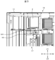
- FIG. 1 is a diagram for explaining a substrate processing apparatus according to an embodiment.
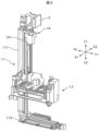
- FIG. 2 is a perspective view of a cassette stage and a cassette transport device according to the embodiment.
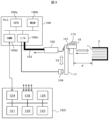
- FIG. 3 is a block diagram of a control system for wafer mapping using a laser sensor.
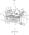
- FIG. 4 is a perspective view of the cassette transfer unit according to the embodiment.
- FIG. 5 is a perspective view of the comb sensor and the wafer attitude aligning device provided on the cassette stage.
- FIG. 6 is a diagram showing a wafer detection flow by a laser sensor.
- FIG. 7 is a diagram showing a process flow of a substrate processing method according to an embodiment.
- FIG. 8 is a diagram showing a boat MAP displayed on the screen by the main control unit.
- FIG. 9 is a diagram for explaining the arrangement of laser sensors in a modified example, and is a cross-sectional view of a main part of a side surface of a substrate processing apparatus.
- a substrate processing apparatus (hereinafter also simply referred to as a processing apparatus) is configured as, for example, a semiconductor manufacturing apparatus that performs processing steps in a manufacturing method for semiconductor devices.
- the cassette transfer unit 12 has a cassette stage device (also called a cassette loader or I/O port) 13 that can hold two open cassettes (hereinafter simply referred to as cassettes) 2 as substrate containers that are carriers for wafers 1 as substrates, and two wafer posture alignment devices 14 are provided below the cassette stage device 13.
- the mounting table 44 (described later) of the cassette stage device 13 receives the cassette 2 transported by an external transport device (not shown) in a vertical position (with the wafers 1 stored in the cassette 2 vertical).
- the placement table 44 (described later) of the cassette stage device 13 receives the cassette 2 transferred by an external transfer device (not shown) in a vertical position (a state in which the wafers 1 stored in the cassette 2 are vertical).
- the wafer position alignment device 14 aligns the position of the wafer 1 stored in the vertically oriented cassette 2 so that the notch and orientation flat (hereinafter referred to as orientation flat, etc.) of the wafer 1 are the same.
- the placement table 44 is configured to be able to rotate the cassette 2 by 90 degrees between a vertical position and a horizontal position (a state in which the wafers 1 stored in the cassette 2 are horizontal and the access opening of the cassette 2 faces the X2 direction).
- a cassette shelf 15 is provided opposite the cassette transfer unit 12, and a spare cassette shelf 16 is provided above the cassette transfer unit 12.
- a cassette transport device 17 is provided between the cassette delivery unit 12 and the cassette shelf 15.
- the cassette transport device 17 is equipped with a robot arm 18 that can move a horizontally oriented cassette forward and backward (X1-X2 direction), and the robot arm 18 itself is configured to be able to move laterally and ascend and descend.
- the robot arm 18 transports the cassette 2, which is in a horizontal position on the cassette stage device 13, to the cassette shelf 15 or spare cassette shelf 16 by moving forward and backward (forward and backward), ascending and descending, and descending.
- the cassette shelf 15 and spare cassette shelf 16 function as buffers that store the transported wafers in the cassettes used for transporting them to the processing equipment until they are needed.
- a wafer transfer device 19 In the transfer chamber 50, a wafer transfer device 19, a wafer holding section 20, a wafer holding plate 21, a boat elevator 22, etc. are installed.
- the wafer transfer device (transfer machine) 19 is installed behind the cassette shelf 15 (X2 side) so that it can rotate and rise and fall, and transfers the wafers 1 in the cassette 2 to a substrate support (hereinafter referred to as a boat) 25, either all at once or one by one.
- the wafer transfer device 19 is equipped with an advance/retract mechanism 20 that moves the multiple wafer holding plates 21 back and forth, and can access the facing cassette 2 in the cassette shelf 15 through an opening in the wall section 70.
- the processing apparatus 10 is equipped with a reaction tube (processing tube) 31 made of a highly heat-resistant material such as quartz or SiC, and the reaction tube 31 is arranged vertically so that the tube axis is vertical.
- the cylindrical hollow portion of the reaction tube 31 forms a processing chamber 32 in which multiple wafers 1 are accommodated, and the lower end of the reaction tube 31 opens into the transfer chamber 50 and forms a furnace port 33 for loading and unloading the wafers 1.
- the furnace port 33 is closed by a seal cap 24.
- a boat 25 for holding the wafers 1 is supported vertically on the seal cap 24.
- the boat 25 has a pair of upper and lower end plates 26, 27, and multiple holding members (pillars) (three in this embodiment) that are vertically arranged between the end plates 26, 27, and each holding member has multiple holding grooves that are equally spaced in the longitudinal direction and recessed so that they open opposite each other.
- the wafers 1 are held aligned horizontally and with their centers aligned within the boat 25 by inserting their outer peripheral edges between the multiple holding grooves of each holding member.
- the cassette transport device 17 includes a CZ drive unit 171 that moves the robot arm 18 up and down (Z1-Z2 direction), and a CS drive unit 172 that moves the CZ drive unit 171 left and right (Y2-Y1 direction).
- This allows the robot arm 18 to access a cassette at any position by moving forward and backward, horizontally, and vertically.
- the laser sensor 101 is provided at the base of the robot arm 18, facing in the X1 direction, at a predetermined distance (d) from the wafer 1.
- the laser sensor 101 may be provided on the robot's hand 173 and made movable forward and backward.
- the wafers 1 stored in the cassette 2 placed on the cassette stage device 13 are in a horizontal state.
- the laser sensor 101 is a reflective sensor that irradiates a laser beam (reference beam) substantially parallel to the main surface of the wafer 1 in the forward direction (X1 direction) and receives the laser beam reflected from the end surface of the wafer 1.
- the laser sensor 101 has, for example, a light-projecting circuit, a light-projecting element controlled by the light-projecting circuit, a light-receiving element that receives the reflected light, and a light-receiving circuit that outputs the amount of received light.
- the laser sensor 101 is preferably a limited reflective sensor having a detection area that spreads flatly within one plane and within a predetermined distance.
- the sub-control unit 100 of the processing device 10 will be explained using FIG. 3.
- the control program that controls the operation of the mapping device and the like are stored in a readable manner in the storage device 100b.
- the storage device 100b is configured as a tangible computer-readable recording medium.
- the I/O unit 100c includes an analog input unit, a contact input unit, etc., which are connected to the laser sensor 101 and the trigger sensor 104, etc.
- the communication unit 100d is a device that communicates with the main control unit 120 provided in the processing device 10.
- the main control unit 120 is configured as a computer equipped with a CPU 121, a main memory device 122, etc.
- the main control unit 120 is configured to control the rotational operation of the mounting table 44, the wafer attitude alignment device 14, the operation control of the robot arm 18 of the cassette transport device 17, the rotation and elevation control of the wafer transfer device 19, the elevation operation of the boat elevator 22, the sub-controller 100, etc., via the communication unit 124 and I/O unit 125, by the CPU 121 reading and executing a program, recipe, and WAP (described later) from the auxiliary storage device 123 into the main storage device 122, and to perform processing based on the recipe.
- a recipe is prepared for each type of processing performed by the processing device.
- the main control unit 120 can be connected to be able to communicate with a higher-level control device (not shown) that manages the manufacturing process of the semiconductor device.
- the auxiliary storage device 123 can include a recording medium such as an optical disk or a USB memory.
- the high-temperature mode and the low-temperature mode can be automatically switched depending on whether the processing temperature is higher or lower than the upper limit of the usable temperature of Si wafers.
- the usable temperature means a temperature at which the wafer and the processing chamber 32 can be used without being damaged when the wafer is placed in the processing chamber 32 and the desired processing is performed.
- the operation mode can be automatically selected according to the processing temperature or WAP set in the main control unit 120, or can be manually set through the HMI (Human Machine Interface) 126 regardless of the processing temperature. If a cassette containing Si wafers made of prohibited material is loaded during operation in the high temperature mode, the main control unit 120 controls the processing device 10 to eject the cassette.
- HMI Human Machine Interface
- Two hinge members 35 are fixed to the top and bottom of the outer surface of the right side plate 39 at the end on the front plate 41 side.
- Two hinge members 36 are fixed to the front side (X1 direction side) of the housing 11 shown in Figure 1 and are connected to the corresponding hinge members 35.
- the cassette stage device 13 is rotatably supported relative to the housing 11 by the hinge members 35, which are rotatable around axes in the Z1-Z2 directions.
- the rotating shaft 49 supports the mounting table 44 on the left side plate 38 and the right side plate 39 so that the mounting table 44 can rotate around the CY axis.
- the mounting table 44 is equipped with a pair of rotating plates 45a, 45b, an internal transfer stage 46, an external transfer stage 47, and a lower plate 48.
- the rotating plates 45a, 45b are fixed to the rotating shaft 49 on the CY axis, and are rigidly connected between them by the lower plate 48.
- the mounting table 44 can rotate around the rotating shaft 49.
- the internal transfer stage 46 is fixed to the rotating plates 45a, 45b and/or the lower plate 48.
- the external transfer stage 47 is attached to the horizontally-positioned rotating plates 45a, 45b via a plurality of guides 51 that allow movement in only one direction so that the cassette can move up and down in a vertical position.
- the air cylinder 52 is provided between the internal transfer stage 46 and the external transfer stage 47, and drives the external transfer stage 47 up and down. Two cassettes 2 can be placed on the internal transfer stage 46 and the external transfer stage 47.
- Two wafer alignment holes 53 are provided at a specified interval on the external transfer stage 47. Below the wafer alignment holes 53, the wafer posture alignment device 14 is provided on the lower plate 48.
- a drive unit 65 that rotates the rotation shaft 49 is attached to the outer surface of the right side plate 39.
- the drive unit 65 includes, for example, an AC servo motor, a worm gear box, a position sensor, etc., and is configured to be able to rotate the cassette 2 on the mounting table 44 by 90 degrees between a horizontal position and a vertical position.
- the wafer posture alignment device 14 comprises a support table 141, a pair of rollers 142a, 142b rotatably suspended horizontally across the support table 141, a rotation drive device 143, and a stopper 144 provided adjacent to the roller 142b.
- the pair of rollers 142a, 142b extend in the alignment direction (X1-X2 direction) of the group of wafers 1 stored in the cassette 2.
- the rotation drive device 143 synchronously rotates the rollers 142a, 142b in the same direction.
- the wafer posture alignment device 14 is configured to be able to rise and fall relative to the cassette 2 placed on the mounting table 44.
- the wafer position alignment device 14 is raised so that the multiple wafers 1 inside the cassette 2 placed on the cassette stage device 13 come into contact with the rollers 142a, 142b, and the wafers 1 are rotated in the same direction by both rollers 142a, 142b, aligning the orientation flats between the multiple wafers 1 to a fixed position.
- the orientation flat alignment is performed mechanically by rotating the rollers 142a, 142b so that the wafer 1 rotates one or more times, and when the orientation flats match, the rotation is restricted by the stopper 144, which acts as a stopper, causing the rollers 142a, 142b to rotate freely. Notch alignment is also achieved by a similar mechanism.
- the wafer posture alignment device 14 is provided with a comb sensor 111 that detects the presence or absence of a wafer 1 of a predetermined material in the cassette 2 before wafer posture alignment (when the wafer 1 is in a vertical state), and is installed so as not to mechanically interfere with the cassette 2 placed on the cassette stage device 13.
- the comb sensor 111 is attached to the side of the support table 141 on the roller 142a side (Y2 side) so that it can move up and down relative to the cassette 2. It can move between a detection position and a retreat position so that it can detect all sizes of wafers included in the detection parameters described below. This allows it to be used commonly for wafers of different diameters, improving versatility. Wafer mapping by the comb sensor 111 is performed with the cassette 2 in a different posture than that of wafer mapping by the laser sensor 101. This allows the comb sensor 111 to be provided in a different position from the laser sensor 101.
- the comb sensor 111 is configured in a comb shape with multiple pairs of transmission type photoelectric sensors, each consisting of a light emitting section and a light receiving section, arranged in the direction in which the wafers 1 are arranged, corresponding to the number of wafers 1 that can be accommodated in the cassette 2.
- the opposing light emitting section and light receiving section detect the presence or absence of each wafer 1 on the optical path between them.
- the light emitting section is configured, for example, by a near-infrared or visible light emitting diode, and the light receiving section is configured, for example, by a phototransistor.
- the light emitting unit is arranged in the area where the wafer 1 is placed, in this example, on one side of the storage area (slot) of each wafer 1 in the cassette 2.
- the light receiving unit is arranged so as to face the light emitting unit through the storage area of the wafer 1 on the incident optical path of the light from the light emitting unit.
- the light emitting unit and the light receiving unit are arranged so that the light emitting surface of the light emitting unit faces the first surface of the wafer 1 and the light receiving surface of the light receiving unit faces the second surface opposite the first surface of the wafer 1.
- the comb sensor 111 is configured to be movable relatively to the cassette 2 on the cassette stage device 13 between a detection position where the substrate can be detected and a retreat position.
- the detection position can be a position that can be commonly applied to wafers of all sizes.
- the comb sensor 111 and the air cylinder 52 constitute a first mapping device.
- the first mapping device and the second mapping device are collectively called mapping devices.
- the comb sensor 111 is a transmission type sensor that irradiates the wafer 1 with reference light and detects the light that has passed through the wafer 1.
- the light receiving unit receives (detects) the light emitted (reference light) from the light emitting unit when the wafer 1 is not present, and does not receive (detect) the light emitted (reference light) from the light emitting unit when the wafer 1 is present.
- the presence or absence of the wafer is actually determined by threshold processing of the amount of received light designed for a silicon wafer, which has a transmittance of 0 for the reference light.
- the wafer 1 is a transparent wafer (e.g., a quartz wafer)
- the amount of transmitted light exceeds the threshold, so the presence or absence of the wafer cannot be determined.
- detection of SiC wafers, which have a transmittance between silicon and quartz is not guaranteed.
- the presence or absence of a wafer and its type are determined by combining the detection of the comb sensor 111 and the laser sensor 101. Wafer mapping using the laser sensor 101 will be explained below with reference to FIG. 6 and Tables 1 to 3. The wafer mapping in the following explanation is performed under the control of the main control unit 120 and the sub-control unit 100.
- Step S10 The main control unit 120 prepares information on the cassette type and the presence/absence and type of wafers in each slot as setting information for the inserted cassette.
- the information on which these are based is notified each time from the upper control device of the processing device 10, or is set in advance as WAP (wafer arrangement parameters) in the device, or is input by a person when the cassette is inserted, as will be described later in detail.
- WAP wafer arrangement parameters
- the master data is a parameter required for detecting a wafer from the sensor output obtained in time series by the lifting and lowering operation of the laser sensor 101, and is empirically created based on the sensor output and detection results when normal detection was performed in advance, and is registered for each combination of size and material. This makes it possible to configure a general-purpose sensor system simply by replacing the master data.
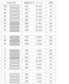
- the master data consists of the cassette table shown in Table 1 and the detection parameter table shown in Table 2.
- the cassette table specifies the specifications of cassettes, which differ for each wafer size.
- "Cassette” in the first column is the name that identifies the cassette, and is listed here from A to D.
- the second column holds the number of slots.
- "Slot spacing” in the third column is the width of the slot (also called pitch), and is in units of 0.05 mm. For example, 127 means 6.35 mm.
- Reference slot height is the height of the lowest slot from the bottom end of cassette 2, and is in units of 0.05 mm.
- Step S11 The main control unit 120 moves the robot arm 18 to a position slightly below the trigger sensor 104 as appropriate, and instructs the sub-control unit 100 to prepare for scanning. After that, the robot arm 18 is raised at a constant speed.
- the sub-control unit 100 turns on the light projection of the laser sensor 101, and starts sampling the light receiving intensity of the laser sensor 101 at the timing when the trigger sensor 104 such as a dog sensor detects the passage of the reference position. Since the laser sensor 101 is a reflective sensor, the light receiving intensity (amount of light received) is large where the wafer 1 is present, and the light receiving intensity is small where the wafer 1 is not present.
- the data is acquired as scan data.
- the minimum drive unit, lifting speed, and sampling rate of the CZ drive unit are designed so that the data of the light receiving intensity can be obtained at intervals of 0.05 mm. This allows a position resolution in the height direction of 0.05 mm to be achieved, as described later.
- Step S12 The main control unit 120 performs threshold processing (binarization processing) on the scan data acquired from the sub-control unit 110, and extracts the section where the scan data continuously exceeds the threshold as detection data.
- the detection data corresponds to the thickness of the wafer 1.
- the threshold used here is common to all combinations of substrate sizes and materials. This is because the reflection intensity from the end face has a relatively low dependency on the substrate size and material.
- Step S13 The position of each slot is calculated by referring to the cassette table of the master data shown in Table 1, and the detection data obtained in step S12 is applied to each slot. To be precise, the cassette is first specified by referring to the master data shown in Table 2, and then the cassette table is referred to.
- Step S14 From the detection data for each slot, the presence (ON)/absence (OFF)/abnormality of wafer 1 is judged for each slot by referencing the detection parameter table of the master data shown in Table 2. If there is no detection data for a slot, it is determined that there is no wafer 1. If there is multiple pieces of detection data for a slot or if the detection data does not fall within the allowable range of the detection parameter table, it is determined to be an abnormal slot.
- the detection parameter table holds parameters for each type of wafer, that is, for each combination of material and size, and the "Register No.” in the first column uniquely identifies the type of wafer.
- the parameters are quantitatively given from the pattern of light receiving intensity obtained by repeating step S11 for a known wafer 1 normally stored in a slot of the cassette 2.
- the standard light receiving pattern is obtained, for example, by averaging multiple scan data of the light receiving intensity.
- the wafer under reference value (micro-lower value) is defined as the position where the light receiving intensity crosses the threshold while increasing, that is, the lower end of the wafer 1
- the wafer on reference value (micro-upper value) is defined as the position where the light receiving intensity crosses the threshold while decreasing, that is, the upper end of the wafer 1
- the peak intensity can be defined as the maximum light receiving intensity between the micro-lower value and the micro-upper value.
- the "intermediate position offset" can be defined as the distance by which the intermediate position of the interval where the light receiving intensity exceeds the threshold is shifted from the slot position of the cassette 2.
- the fifth column in the detection parameter table is the lower limit of the difference between the micro-upper and micro-lower values for each type of wafer.
- the sixth column, "Micro-upper-lower interval (max),” is the upper limit of the difference.
- the "Peak Intensity (min)” in the seventh column and the “Peak Intensity (max)” in the eighth column are the lower and upper limits of the peak intensity for each type of wafer, and are calculated and registered based on the average value, standard deviation, or measured minimum and maximum values.
- the "Mid-position offset (min)" in the ninth column and the “Mid-position offset (max)” in the tenth column are the lower and upper limits of the mid-position offset for each type of wafer, and are calculated and registered based on the average value, standard deviation, or measured minimum and maximum values.
- the mid-position offset may include half the wafer thickness as a positive biasing factor, and the amount of wafer deflection as a negative biasing factor.
- the "Peak center shift (max)" in the 11th column is a value indicating the upper limit of the difference (absolute value) between the position of the peak intensity and the midpoint of the interval where the received light intensity exceeds the threshold for each type of wafer, and is calculated and registered based on the average value, standard deviation, etc.
- the peak appears when the optical axis of the laser sensor 101 is perpendicular to the edge of the wafer. For wafers with edges of a typical shape, this difference is distributed around 0. A shift that exceeds the peak center shift (max) suggests an abnormality such as wafer tilt.
- the registered detection parameter table includes "material,” “size,” and “cassette” in addition to the above.
- material is the material of the wafer 1, such as silicon (Si) or silicon carbide (SiC).
- Size is the diameter of the wafer 1, and is expressed in mm.
- micro-up-micro-down interval (min) "micro-up-micro-down interval (max)"
- peak intensity (min) “peak intensity (max)”
- peak intensity (max) “middle position offset (min)”
- middle position offset (max) “middle position offset (max)”
- peak center shift (max) is given in units of 0.05 mm.
- the above-mentioned detection parameters are acquired in advance for multiple combinations of wafer size and material, and cassette, and are stored in the memory device of the main control unit 120 or the memory device 100b of the sub-control unit 100 in the data structure shown in Table 2.
- step S14 refers to the information on the cassette type and wafer type of each slot acquired in S11, and while appropriately switching the detection parameters for each slot, judges whether the detection data is within the allowable range of the detection parameters. If one or more items are outside the allowable range, the sub-controller 100 judges the slot to be abnormal and issues a warning. Note that the level of the warning may be varied depending on the items that are outside the allowable range and the number of items. Also, the detection parameters used are basically those that correspond to the setting information, but if an abnormality is detected, the judgment is made using the detection parameters of a different material of the same size, and if they are present (ON), this may be set as the final value.
- Step S15 The material (type) of the wafer is determined for each slot using the determination table shown in Table 3. If the wafer mapping by the laser sensor 101 is determined to be ON and the wafer mapping by the comb sensor 111 is determined to be ON, the material of the wafer 1 is determined to be Si. If the wafer mapping by the laser sensor 101 is determined to be ON and the wafer mapping by the comb sensor 111 is determined to be OFF, the material of the wafer 1 is determined to be SiC. If the wafer mapping by the laser sensor 101 is determined to be OFF and the wafer mapping by the comb sensor 111 is determined to be OFF, it is determined that there is no wafer 1.
- the thickness of the wafer 1 may be determined from the detection data extracted in step S12, and the material of the wafer 1 may be determined by referring to information that associates the thickness of the wafer 1 with the material of the wafer 1 (detection parameter data shown in Table 2). In the example shown in Table 2, the material can be determined from the peak intensity alone, but this may be difficult to determine. If the material can be determined from the wafer thickness or peak intensity, the comb sensor 111 is not required, and the presence or absence and material of the wafer 1 may be determined using only the laser sensor 101.
- the cassette may be a specific-purpose carrier that stores only one of the above-mentioned wafers, or a mixed carrier that stores wafers with different purposes that are placed in a boat together in one batch process. Assuming that only specific-purpose carriers are used, one batch process requires, for example, four product wafer cassettes (P01, P02, and P03) including three carrier types, one dummy wafer cassette (S01), and one monitor wafer cassette (M01).
- P01, P02, and P03 product wafer cassettes
- S01 dummy wafer cassette
- M01 monitor wafer cassette
- virtual carriers These are called virtual carriers or logical carriers, and are defined as alias information associated with carrier types such as "product,”"dummy,” and “monitor.”
- the main control unit 120 associates the virtual carrier with information indicating the type and material of the wafer, assuming that only wafers of a single material are stored therein, and holds the alias information.
- a virtual carrier When a mixed carrier is used, a virtual carrier is defined in the same manner by associating it with a carrier type corresponding to the type of the majority of wafers. Furthermore, a slot map indicating which slot stores which wafers for which purposes and materials, is defined for each virtual carrier, and the main control unit 120 holds the alias information by linking it to the slot map.
- the slot map may be specified based on mapping by the processing device itself without prior information.
- the alias information and slot map may be stored in advance in the main control unit 120 as part of the information constituting the WAP, or may be notified from a higher-level control device of the processing device 10.
- the WAP depends on the contents of the substrate processing. In other words, a WAP is linked to each recipe.
- cassette insertion S20
- a cassette 2 loaded with unprocessed wafers 1 is placed on a cassette stage device 13 of a cassette transfer unit 12 with the help of an external transfer device (not shown) or a person.
- the wafers 1 in the cassette 2 are in a vertical position.
- information indicating which virtual carrier the placed cassette corresponds to or the material of each stored wafer is given from a higher-level control device or a person.
- wafer alignment S22
- the wafer 1 is aligned by the wafer position alignment device 14 using an orientation flat or the like.
- step S25 If the processing apparatus 10 is operating in the high temperature mode and the wafer determined in S24 contains the prohibited material (Si), it is determined to be abnormal, and the process branches to step S36. If there is a slot in which the material and presence of the wafer specified from the carrier information and the like do not match the material and presence of the wafer determined in S24, it is determined that there is an abnormality, and the process branches to step S37. In step S25, the substrate in the carrier (corresponding carrier) that was brought into the processing apparatus as corresponding to the virtual carrier is transferred to the substrate holder based on the map information. In addition, when the operation mode is the low temperature mode, S24 is omitted, and only the presence or absence of a wafer is judged based on the result of S21. may be compared to judge whether there is an abnormality.
- a cassette associated with a virtual carrier may be stored at a position such as the cassette shelf 15 that is fixedly assigned to that virtual carrier.
- the main control unit 120 controls the robot arm 18 to sequentially move the cassettes associated with each virtual carrier from the cassette shelf 15 or the spare cassette shelf 16 to a transfer shelf located at a position facing the wafer transfer device 19 of the cassette shelf 15.
- the wafers 1 in the cassettes 2 placed on the transfer shelf are sequentially transferred to the boat 25 by the wafer transfer device 19.
- the main control unit 120 controls the wafer transfer device 19 by referring to a boat MAP as map information indicating which slot of which virtual carrier the wafers should be transferred from for each slot of the boat.
- the boat MAP can be defined in advance by direct specification, or can be dynamically generated based on the WAP.
- the boat MAP and the WAP constitute substrate arrangement information.
- the virtual carrier referred to by the substrate placement information and the information on the material of the wafers contained in the virtual carrier are linked by alias information, etc., and since it has been confirmed in S25 that the information on the material matches the first information, the substrate placement information and the first information are linked as a result. In other words, the wafer is transferred with the material correctly understood.
- WAP is a general term for parameters that conceptually define the relationship between the type of wafer and the slot of the boat to be placed in rather than directly specifying it.
- WAP the remaining wafers in the cassette that were not used in the previous batch process can be dynamically determined as the target for transfer. It is sufficient for WAP to specify the type of wafer, and it is not necessary for it to specify the material.
- CAP cassette placement information
- an appropriate measure is selected. Specifically, when a WAP is directly specified and there is a mismatch in material or a missing wafer, it is determined that the current batch process cannot be continued, and the process proceeds to S39. When a WAP is not directly specified, in other words, when dynamic placement is possible, it is determined that the current batch process can be continued, and the process returns to S26. In this case, the boat MAP is corrected so that wafers or cassettes that are insufficient due to a mismatch or the like are replaced with wafers or cassettes of the same type. If there are insufficient replacement wafers or cassettes, an alarm is sounded to prompt the insertion of cassettes, and the process may be interrupted until a sufficient amount is inserted.
- cassette dispensing S39 If it is determined in S37 that the material is prohibited or that the process cannot be continued, the corresponding cassette is ejected. That is, the cassette stage device 13 is controlled to rotate the cassette 2 by 90 degrees so that the access opening faces upward, making the cassette 2 removable, and an alarm or the like is issued to prompt an external transport device or the like to carry out the cassette on the cassette stage device 13 to the outside of the housing 11.
- the cassettes to be ejected are only the cassettes determined to be abnormal in S25, or the set of cassettes including the abnormal cassette that were to be used in the corresponding batch process. The alarm is not released until the target cassette is ejected or some kind of recovery operation is performed.
- the dispensing of S39 can also be postponed.
- the cassette can be temporarily stored in the cassette shelf 15 or the like after being made unavailable for selection in batch processing by, for example, canceling the association with the virtual carrier. This makes it possible to avoid impeding the insertion of subsequent cassettes.
- the abnormality determination of S25 can be postponed until all virtual carrier mapping (S24) for one batch process is complete.
- the wafer material can be recognized and transported from the processing equipment I/O port to the boat, allowing the equipment to be operated flexibly and efficiently by using specific-purpose carriers containing wafers of one material or mixed carriers containing wafers of multiple materials.
- wafers provided by virtual carriers can be transferred to appropriate slots in a boat to provide a multi-wafer material handling device.
- a WAP is selected according to the recipe, and the material of the wafers to be transferred to the boat is identified by the WAP, making it possible to automatically switch operation modes based on the material and processing temperature. For example, if there is a recipe for processing only Si wafers and a recipe for processing only SiC wafers, the former will operate in low-temperature mode and the latter in high-temperature mode. This allows the equipment to be used for both SiC and Si, further improving the equipment operating rate.
- the laser sensor 101 is a scanning type, and since it compares and judges with master data, it can detect regardless of the board material. This makes it possible to detect the positions of multiple types of boards without changing the hardware. In other words, the software can handle differences in board size and cassette pitch.
- the laser sensor 101 uses an edge reflection type sensor, so it is possible to detect the presence or absence of a substrate with a single edge reflection type sensor even for substrates with high transmittance (e.g., quartz wafers), transparent substrates whose transmittance changes due to film formation (e.g., SiC wafers), and substrates with low transmittance (Si wafers).
- substrates with high transmittance e.g., quartz wafers
- transparent substrates whose transmittance changes due to film formation e.g., SiC wafers
- Si wafers substrates with low transmittance
- the thickness of the substrate can be measured based on the intensity of light received by the reflective sensor, so the substrate material can be determined based on differences in substrate thickness.
- Two types of wafer mapping can distinguish the substrate material (Si wafer and SiC wafer, or Si wafer and quartz wafer). This eliminates the need to prepare a dedicated comb sensor for each substrate material in order to distinguish the substrate material. This helps prevent the cassette stage from becoming too large.
- the laser sensor 101 is fixed to the housing 11 on the front side (X1 side) of the processing apparatus 10 with respect to the cassette transport device 17.
- the laser sensor 101 is fixed to the housing 11 on the opposite side of the cassette shelf 15 with respect to the cassette transport device 17.
- the optical axis of the laser sensor 101 is fixed in the horizontal direction, and reference light is irradiated in the X2 direction.
- the laser sensor 101 irradiates the reference light to the cassette 2 on the robot arm 18 of the cassette transport device 17.
- the cassette transport device 17 raises and lowers the cassette 2, thereby performing wafer mapping within the cassette 2. In this embodiment as well, the same effect as the above embodiment can be obtained.
- the wafer 1 is fixed and the laser sensor 101 can be raised and lowered, but in this embodiment, the laser sensor 101 is fixed and the wafer 1 can be raised and lowered. In other words, the laser sensor 101 can move relative to the wafer 1 stored in the cassette 2 along the arrangement direction of the wafer 1.
- wafer mapping by the laser sensor 101 is performed when the cassette 2 is in the cassette stage device 13, but in this embodiment, it is performed when the cassette 2 is in the cassette transport device 17. In either case, wafer mapping by the laser sensor 101 is performed when the cassette 2 is in a location that cannot be accessed by the wafer transfer device 19, that is, when it is in a location other than the transfer shelf. This allows wafer mapping to be performed without occupying the transfer shelf or transfer device 17, so there is no delay in transferring the wafers. Furthermore, in this embodiment, it can be performed without occupying the cassette stage device 13, so there is no delay in inserting or removing the cassette.
- a laser sensor 101 is used to detect reflections from the edge of a wafer in wafer mapping
- the present disclosure is not limited to the above embodiments.
- a reflector may be placed outside the opening at the bottom of the cassette to detect light that has made one round trip through the gap between adjacent wafers.
- the embodiment is the same as the above embodiment, except that the intensity of the received light level is reversed.
- the laser sensor 101 irradiates the reference light toward the center of the wafer at the lateral center, which is the closest point to the edge of the wafer, in other words, detects the reflection from the edge perpendicular to the reference light, but the present disclosure is not limited to the above-mentioned embodiments.
- Examples of batch-type substrate processing apparatuses that process multiple substrates at a time have been described.
- the present disclosure is not limited to the above-mentioned embodiments, and can also be applied, for example, to single-wafer type substrate processing apparatuses that process one or several substrates at a time.
- Single-wafer type apparatuses may not have cassette shelves or cassette transport devices, but can perform mapping with material discrimination as disclosed herein using a substrate transfer machine or other mapping means within a load port or vacuum load lock chamber.
- each process can be performed using the same process procedures and conditions as in the above-mentioned embodiment, and the same effects as in the above-mentioned embodiment can be obtained.
Landscapes
- Container, Conveyance, Adherence, Positioning, Of Wafer (AREA)
Priority Applications (5)
| Application Number | Priority Date | Filing Date | Title |
|---|---|---|---|
| KR1020257036564A KR20260029272A (ko) | 2023-06-30 | 2023-10-19 | 기판 처리 장치, 매핑 장치, 기판 처리 방법, 반도체 장치의 제조 방법 및 프로그램 |
| EP23943779.1A EP4738430A1 (en) | 2023-06-30 | 2023-10-19 | Substrate processing device, mapping device, substrate processing method, semiconductor device manufacturing method, and program |
| JP2025529413A JPWO2025004393A1 (cg-RX-API-DMAC7.html) | 2023-06-30 | 2023-10-19 | |
| CN202380094579.XA CN120731503A (zh) | 2023-06-30 | 2023-10-19 | 基板处理装置、映射装置、基板处理方法、半导体器件的制造方法及程序 |
| US19/327,525 US20260018440A1 (en) | 2023-06-30 | 2025-09-12 | Substrate Processing Apparatus, Mapping Apparatus, Substrate Processing Method, Method of Manufacturing Semiconductor Device and Non-transitory Computer-readable Recording Medium |
Applications Claiming Priority (2)
| Application Number | Priority Date | Filing Date | Title |
|---|---|---|---|
| JP2023-107929 | 2023-06-30 | ||
| JP2023107929 | 2023-06-30 |
Related Child Applications (1)
| Application Number | Title | Priority Date | Filing Date |
|---|---|---|---|
| US19/327,525 Continuation US20260018440A1 (en) | 2023-06-30 | 2025-09-12 | Substrate Processing Apparatus, Mapping Apparatus, Substrate Processing Method, Method of Manufacturing Semiconductor Device and Non-transitory Computer-readable Recording Medium |
Publications (1)
| Publication Number | Publication Date |
|---|---|
| WO2025004393A1 true WO2025004393A1 (ja) | 2025-01-02 |
Family
ID=93938329
Family Applications (1)
| Application Number | Title | Priority Date | Filing Date |
|---|---|---|---|
| PCT/JP2023/037795 Ceased WO2025004393A1 (ja) | 2023-06-30 | 2023-10-19 | 基板処理装置、マッピング装置、基板処理方法、半導体装置の製造方法およびプログラム |
Country Status (6)
| Country | Link |
|---|---|
| US (1) | US20260018440A1 (cg-RX-API-DMAC7.html) |
| EP (1) | EP4738430A1 (cg-RX-API-DMAC7.html) |
| JP (1) | JPWO2025004393A1 (cg-RX-API-DMAC7.html) |
| KR (1) | KR20260029272A (cg-RX-API-DMAC7.html) |
| CN (1) | CN120731503A (cg-RX-API-DMAC7.html) |
| WO (1) | WO2025004393A1 (cg-RX-API-DMAC7.html) |
Cited By (1)
| Publication number | Priority date | Publication date | Assignee | Title |
|---|---|---|---|---|
| WO2026159767A1 (ja) * | 2025-01-21 | 2026-07-30 | 株式会社Kokusai Electric | 基板処理方法、基板処理装置、半導体装置の製造方法およびプログラム |
Families Citing this family (1)
| Publication number | Priority date | Publication date | Assignee | Title |
|---|---|---|---|---|
| CN122149411A (zh) * | 2026-05-11 | 2026-06-05 | 宸微设备科技(苏州)有限公司 | 水平度检测装置和水平度调节方法、以及半导体设备 |
Citations (12)
| Publication number | Priority date | Publication date | Assignee | Title |
|---|---|---|---|---|
| JPS63150094A (ja) | 1986-12-12 | 1988-06-22 | ブラザー工業株式会社 | 縫い位置確認機能を備えたミシン |
| JPH11121593A (ja) * | 1997-10-13 | 1999-04-30 | Mitsui Eng & Shipbuild Co Ltd | ウェハ検出方法および装置 |
| US6560507B1 (en) * | 2000-10-20 | 2003-05-06 | Novellus Systems Inc. | Module classification approach for moving semiconductor wafers in a wafer processing system |
| JP2011171648A (ja) | 2010-02-22 | 2011-09-01 | Hitachi Kokusai Electric Inc | 基板処理システム |
| JP2011211048A (ja) * | 2010-03-30 | 2011-10-20 | Kawasaki Heavy Ind Ltd | 基板搬送ロボットの状態監視装置 |
| JP2012182351A (ja) | 2011-03-02 | 2012-09-20 | Hitachi Kokusai Electric Inc | 基板処理装置及び基板移載方法。 |
| JP2013230036A (ja) * | 2012-04-26 | 2013-11-07 | Tokyo Electron Ltd | モータ制御装置、モータ制御方法及び記憶媒体 |
| JP2015106575A (ja) | 2013-11-28 | 2015-06-08 | 株式会社日立国際電気 | 基板処理装置、基板処理装置の制御方法、制御プログラム及び半導体装置の製造方法 |
| WO2018154829A1 (ja) | 2017-02-24 | 2018-08-30 | 株式会社Kokusai Electric | 基板処理装置、半導体装置の製造方法及びプログラム |
| JP2020017645A (ja) * | 2018-07-26 | 2020-01-30 | 株式会社Kokusai Electric | 基板処理装置 |
| CN111337994A (zh) * | 2018-12-19 | 2020-06-26 | 合肥欣奕华智能机器有限公司 | 一种基准值校准的方法和设备 |
| JP2022157981A (ja) * | 2021-04-01 | 2022-10-14 | 日本電産サンキョー株式会社 | ワークの搬送装置及びマッピング方法 |
Family Cites Families (1)
| Publication number | Priority date | Publication date | Assignee | Title |
|---|---|---|---|---|
| JPH10150094A (ja) | 1996-11-15 | 1998-06-02 | Kokusai Electric Co Ltd | ウェーハ検出装置 |
-
2023
- 2023-10-19 JP JP2025529413A patent/JPWO2025004393A1/ja active Pending
- 2023-10-19 WO PCT/JP2023/037795 patent/WO2025004393A1/ja not_active Ceased
- 2023-10-19 CN CN202380094579.XA patent/CN120731503A/zh active Pending
- 2023-10-19 KR KR1020257036564A patent/KR20260029272A/ko active Pending
- 2023-10-19 EP EP23943779.1A patent/EP4738430A1/en active Pending
-
2025
- 2025-09-12 US US19/327,525 patent/US20260018440A1/en active Pending
Patent Citations (12)
| Publication number | Priority date | Publication date | Assignee | Title |
|---|---|---|---|---|
| JPS63150094A (ja) | 1986-12-12 | 1988-06-22 | ブラザー工業株式会社 | 縫い位置確認機能を備えたミシン |
| JPH11121593A (ja) * | 1997-10-13 | 1999-04-30 | Mitsui Eng & Shipbuild Co Ltd | ウェハ検出方法および装置 |
| US6560507B1 (en) * | 2000-10-20 | 2003-05-06 | Novellus Systems Inc. | Module classification approach for moving semiconductor wafers in a wafer processing system |
| JP2011171648A (ja) | 2010-02-22 | 2011-09-01 | Hitachi Kokusai Electric Inc | 基板処理システム |
| JP2011211048A (ja) * | 2010-03-30 | 2011-10-20 | Kawasaki Heavy Ind Ltd | 基板搬送ロボットの状態監視装置 |
| JP2012182351A (ja) | 2011-03-02 | 2012-09-20 | Hitachi Kokusai Electric Inc | 基板処理装置及び基板移載方法。 |
| JP2013230036A (ja) * | 2012-04-26 | 2013-11-07 | Tokyo Electron Ltd | モータ制御装置、モータ制御方法及び記憶媒体 |
| JP2015106575A (ja) | 2013-11-28 | 2015-06-08 | 株式会社日立国際電気 | 基板処理装置、基板処理装置の制御方法、制御プログラム及び半導体装置の製造方法 |
| WO2018154829A1 (ja) | 2017-02-24 | 2018-08-30 | 株式会社Kokusai Electric | 基板処理装置、半導体装置の製造方法及びプログラム |
| JP2020017645A (ja) * | 2018-07-26 | 2020-01-30 | 株式会社Kokusai Electric | 基板処理装置 |
| CN111337994A (zh) * | 2018-12-19 | 2020-06-26 | 合肥欣奕华智能机器有限公司 | 一种基准值校准的方法和设备 |
| JP2022157981A (ja) * | 2021-04-01 | 2022-10-14 | 日本電産サンキョー株式会社 | ワークの搬送装置及びマッピング方法 |
Cited By (1)
| Publication number | Priority date | Publication date | Assignee | Title |
|---|---|---|---|---|
| WO2026159767A1 (ja) * | 2025-01-21 | 2026-07-30 | 株式会社Kokusai Electric | 基板処理方法、基板処理装置、半導体装置の製造方法およびプログラム |
Also Published As
| Publication number | Publication date |
|---|---|
| JPWO2025004393A1 (cg-RX-API-DMAC7.html) | 2025-01-02 |
| CN120731503A (zh) | 2025-09-30 |
| KR20260029272A (ko) | 2026-03-04 |
| EP4738430A1 (en) | 2026-05-06 |
| US20260018440A1 (en) | 2026-01-15 |
Similar Documents
| Publication | Publication Date | Title |
|---|---|---|
| JP4313824B2 (ja) | 基板移載装置及び基板移載方法並びに記憶媒体 | |
| JP6040883B2 (ja) | 基板搬送装置、基板搬送方法及び記憶媒体 | |
| KR101245464B1 (ko) | 열처리 장치, 열처리 방법 및 기억 매체 | |
| CN109216237B (zh) | 基板翘曲监视装置、基板处理装置及基板翘曲监视方法 | |
| KR101937066B1 (ko) | 기판 처리 장치 및 기판 처리 방법 | |
| US7547209B2 (en) | Vertical heat treatment system and automatic teaching method for transfer mechanism | |
| US20230290660A1 (en) | Container, container partition plate, substrate processing system, and substrate transfer method | |
| US20260018440A1 (en) | Substrate Processing Apparatus, Mapping Apparatus, Substrate Processing Method, Method of Manufacturing Semiconductor Device and Non-transitory Computer-readable Recording Medium | |
| TWI558469B (zh) | 基板周緣部之塗布膜除去方法、基板處理裝置及記憶媒體 | |
| KR101235774B1 (ko) | 기판 처리 장치 및 기판 처리 장치에 있어서의 이상 표시 방법 | |
| KR101690229B1 (ko) | 기판 반송 방법, 기판 반송 장치 및 기억 매체 | |
| US20240087929A1 (en) | Method of Manufacturing Semiconductor Device and Non-transitory Computer-readable Recording Medium | |
| JP7117841B2 (ja) | ワーク検出装置、成膜装置及びワーク検出方法 | |
| JP4672010B2 (ja) | 半導体製造装置、半導体装置の製造方法および基板の判別方法 | |
| JP4079206B2 (ja) | 基板検査装置および基板検査方法ならびに基板検査装置を備えた液処理装置 | |
| JP2005142245A (ja) | 基板処理装置 | |
| JP2026058368A (ja) | マッピング装置、基板処理装置、マッピング方法、半導体装置の製造方法およびプログラム | |
| JP2002305224A (ja) | ウエハ収納ユニット | |
| JP2011171648A (ja) | 基板処理システム | |
| JP2025006889A (ja) | 基板カセット取扱い装置、基板処理装置、基板処理方法、半導体装置の製造方法およびプログラム | |
| JP7271211B2 (ja) | 基板搬送装置および基板搬送装置の制御方法 | |
| KR20230016882A (ko) | 기판 처리 장치 및 기판 처리 방법 | |
| JP2011119504A (ja) | 基板処理装置 | |
| KR20060094216A (ko) | 웨이퍼 이송 장치 |
Legal Events
| Date | Code | Title | Description |
|---|---|---|---|
| 121 | Ep: the epo has been informed by wipo that ep was designated in this application |
Ref document number: 23943779 Country of ref document: EP Kind code of ref document: A1 |
|
| WWE | Wipo information: entry into national phase |
Ref document number: 2025529413 Country of ref document: JP |
|
| WWE | Wipo information: entry into national phase |
Ref document number: 202380094579.X Country of ref document: CN |
|
| WWP | Wipo information: published in national office |
Ref document number: 202380094579.X Country of ref document: CN |
|
| WWE | Wipo information: entry into national phase |
Ref document number: 2023943779 Country of ref document: EP |
|
| NENP | Non-entry into the national phase |
Ref country code: DE |
|
| ENP | Entry into the national phase |
Ref document number: 2023943779 Country of ref document: EP Effective date: 20260130 |
|
| ENP | Entry into the national phase |
Ref document number: 2023943779 Country of ref document: EP Effective date: 20260130 |
|
| WWP | Wipo information: published in national office |
Ref document number: 2023943779 Country of ref document: EP |