WO2025004324A1 - 電力変換装置、モータ駆動装置及び冷凍サイクル適用機器 - Google Patents
電力変換装置、モータ駆動装置及び冷凍サイクル適用機器 Download PDFInfo
- Publication number
- WO2025004324A1 WO2025004324A1 PCT/JP2023/024379 JP2023024379W WO2025004324A1 WO 2025004324 A1 WO2025004324 A1 WO 2025004324A1 JP 2023024379 W JP2023024379 W JP 2023024379W WO 2025004324 A1 WO2025004324 A1 WO 2025004324A1
- Authority
- WO
- WIPO (PCT)
- Prior art keywords
- voltage
- converter
- power conversion
- current
- conversion device
- Prior art date
- Legal status (The legal status is an assumption and is not a legal conclusion. Google has not performed a legal analysis and makes no representation as to the accuracy of the status listed.)
- Ceased
Links
Images


Classifications
-
- H—ELECTRICITY
- H02—GENERATION; CONVERSION OR DISTRIBUTION OF ELECTRIC POWER
- H02M—APPARATUS FOR CONVERSION BETWEEN AC AND AC, BETWEEN AC AND DC, OR BETWEEN DC AND DC, AND FOR USE WITH MAINS OR SIMILAR POWER SUPPLY SYSTEMS; CONVERSION OF DC OR AC INPUT POWER INTO SURGE OUTPUT POWER; CONTROL OR REGULATION THEREOF
- H02M7/00—Conversion of AC power input into DC power output; Conversion of DC power input into AC power output
- H02M7/02—Conversion of AC power input into DC power output without possibility of reversal
- H02M7/04—Conversion of AC power input into DC power output without possibility of reversal by static converters
- H02M7/12—Conversion of AC power input into DC power output without possibility of reversal by static converters using discharge tubes with control electrode or semiconductor devices with control electrode
Definitions
- This disclosure relates to a power conversion device equipped with a converter that converts AC to DC and outputs the converted DC to a load, a motor drive device equipped with a power conversion device, and a refrigeration cycle application device.
- Power supply current which is the current supplied from an AC power source, contains harmonic currents. Harmonic currents are frequency components with frequencies higher than the fundamental wave frequency. To suppress interference caused by harmonic currents, international regulations have been established for electronic devices that generate harmonic currents. To comply with these regulations, converters take measures to suppress the harmonic currents contained in the power supply current by chopping at AC (Alternating Current) or DC (Direct Current).
- Patent Document 1 discloses a power conversion device equipped with a three-phase PWM (Pulse Width Modulation) converter.
- a three-phase PWM converter is a converter that performs chopping in AC.
- the power supply current is controlled to a sinusoidal shape, making it possible to suppress power supply harmonics, which are harmonic currents contained in the power supply current.
- converters are equipped with one or more semiconductor elements.
- a drive circuit equipped with a drive power supply is required. If a drive power supply is provided independently for each semiconductor element, the drive circuit will become larger, which will lead to a larger converter and therefore a larger power conversion device.
- the present disclosure has been made in consideration of the above, and aims to obtain a power conversion device that can suppress harmonic currents while preventing the device from becoming large.
- the power conversion device includes a converter that converts AC to DC and outputs the DC to a load.
- the converter includes a plurality of first semiconductor elements and a first drive circuit that drives the first semiconductor elements.
- the first drive circuit includes a boot capacitor for applying a drive voltage to upper elements of the first semiconductor elements.
- the boot capacitor is configured to store electric charge by passing a current to the load side of the converter.
- the power conversion device disclosed herein has the effect of suppressing harmonic currents while preventing the device from becoming too large.
- FIG. 1 is a diagram showing a configuration example of a motor drive device including a power conversion device according to a first embodiment
- FIG. 1 is a diagram showing operational waveforms of main parts of a power conversion device according to the first embodiment
- FIG. 1 is a diagram showing a configuration example of a drive circuit provided in a power conversion device according to a first embodiment
- FIG. 4 is a diagram for explaining a charging operation for a boot capacitor of the drive circuit shown in FIG. 3
- FIG. 4 is a diagram for explaining charging control for a boot capacitor of the drive circuit shown in FIG. 3
- FIG. 1 is a block diagram showing an example of a hardware configuration for implementing the functions of a control unit according to a first embodiment
- FIG. 13 is a diagram showing a configuration example of an air conditioner according to a second embodiment.
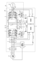
- Embodiment 1. 1 is a diagram showing an example of the configuration of a motor drive device 100 including a power conversion device 50 according to a first embodiment.
- the power conversion device 50 according to the first embodiment is a power conversion device that converts an AC voltage output from a three-phase power supply 110, which is a three-phase AC power supply, into a DC voltage and applies the DC voltage to a load 130.
- the motor drive device 100 according to the first embodiment is a drive device that converts DC power output from the power conversion device 50 into AC power and supplies the converted AC power to a motor 120 to drive the motor 120.
- the phases of the three-phase power supply 110 are represented by R, S, and T, and are called the "R phase", the "S phase”, and the "T phase", respectively.
- the motor drive device 100 includes a noise filter 1, a reactor 2, current detectors 5a and 5b, a phase voltage detector 6, a power converter 50, controllers 14 and 15, and a load 130.
- the load 130 includes a shunt resistor 8 for current detection, an inverter 9, a current detection unit 12, a drive circuit 17 which is a second drive circuit, current detectors 18a and 18b, and a motor 120.
- the shunt resistor 8, the inverter 9, the current detection unit 12, the drive circuit 17, and the current detectors 18a and 18b, excluding the motor 120 are components of the motor drive device 100.
- the noise filter 1 is disposed between the three-phase power supply 110 and the reactor 2.
- the noise filter 1 operates to reduce noise currents flowing in and out of the power conversion device 50.
- the reactor 2 is disposed between the noise filter 1 and the power conversion device 50.
- the reactor 2 is a device that includes circuit elements that temporarily store electrical energy supplied from the three-phase power supply 110. The reactor 2 also operates to reduce noise currents flowing in and out of the power conversion device 50.
- the current detectors 5a and 5b detect the power supply current, which is an alternating current flowing between the three-phase power supply 110 and the power conversion device 50, and output the detection value of the power supply current to the control unit 14.
- An example of the current detectors 5a and 5b is an ACCT (Alternating Current Transformer). Note that FIG. 1 shows an example in which the current detector 5a detects the R-phase current Ir and the current detector 5b detects the T-phase current It, but this example is not limiting.
- the current detectors 5a and 5b only need to detect the current of any two of the three phases, and the current of the remaining phase can be calculated by utilizing the fact that the power supply current is three-phase balanced.
- the phase voltage detection unit 6 detects the R-phase voltage Vr, S-phase voltage Vs, and T-phase voltage Vt, which are the phase voltages of each of the three phases output by the three-phase power supply 110, and outputs the detection values to the control unit 14.
- the power conversion device 50 includes a converter 3, a drive circuit 16 which is a first drive circuit, a capacitor 4, a shunt resistor 7 for current detection, a current detection unit 10, and a voltage detection unit 11.
- the converter 3 converts the AC voltage output from the three-phase power source 110 into a DC voltage and outputs it to the DC buses 19a and 19b.
- the DC buses 19a and 19b are electrical wiring that connect the converter 3 to the load 130.
- the voltage between the DC buses 19a and 19b is called the "bus voltage.”
- Capacitor 4 is connected to DC buses 19a and 19b. Therefore, in the configuration of FIG. 1, the capacitor voltage, which is the voltage across capacitor 4, is equal to the bus voltage. Capacitor 4 smoothes the output voltage of converter 3. The voltage smoothed by capacitor 4 is applied to inverter 9.
- the voltage detection unit 11 detects the bus voltage Vdc and outputs the detected value of the bus voltage Vdc to the control units 14 and 15.
- the converter current I1 flows through the shunt resistor 7.
- the converter current I1 is a current that flows in and out of the converter 3.
- the current detection unit 10 converts the voltage value generated by the converter current I1 flowing through the shunt resistor 7 into a current value and outputs it to the control unit 14.
- the converter 3 comprises six semiconductor elements Q1 to Q6 that are connected in a three-phase bridge.
- the semiconductor elements Q1 and Q2 are connected in series in this order, and the connection point 3a of the semiconductor elements Q1 and Q2 is electrically connected to the R phase of the three-phase power supply 110.
- the semiconductor elements Q3 and Q4 are connected in series in this order, and the connection point 3b of the semiconductor elements Q3 and Q4 is electrically connected to the S phase of the three-phase power supply 110.
- the semiconductor elements Q5 and Q6 are connected in series in this order, and the connection point 3c of the semiconductor elements Q5 and Q6 is electrically connected to the T phase of the three-phase power supply 110.
- the semiconductor elements Q1, Q3, and Q5 arranged on the upper side of the circuit diagram are sometimes referred to as the "upper elements,” and the semiconductor elements Q2, Q4, and Q6 arranged on the lower side of the circuit diagram are sometimes referred to as the "lower elements.”
- the side of the three-phase power supply 110 where the connection points 3a to 3c are located, as viewed from the converter 3, is sometimes referred to as the "AC side,” and the side of the load 130 is sometimes referred to as the "DC side.”
- the semiconductor elements Q1 to Q6 each have diodes D1 to D6 connected in parallel.
- the diodes D1 to D6 are connected so that the anodes are located on the AC side and the cathodes are located on the DC side.
- the semiconductor elements Q1 to Q6 are IGBTs (Insulated Gate Bipolar Transistors), but MOSFETs (Metal Oxide Semiconductor Field Effect Transistors) may be used instead of IGBTs. Note that in the case of MOSFETs, because of their structure they have a built-in parasitic diode, a configuration in which the diodes D1 to D6 are not connected in parallel may also be used.
- the inverter 9 converts DC to AC. More specifically, the inverter 9 converts the DC voltage output from the power conversion device 50 into an AC voltage to be applied to the motor 120 and outputs it.
- An example of a device in which the motor 120 is mounted is a blower or compressor in an air conditioner.
- An air conditioner is an example of a device that applies a refrigeration cycle.
- An inverter current I2 flows through the shunt resistor 8.
- the inverter current I2 is a current that flows in and out of the inverter 9.
- the current detection unit 12 converts the voltage value generated by the inverter current I2 flowing through the shunt resistor 8 into a current value and outputs it to the control unit 15.
- the inverter 9 comprises six semiconductor elements Q21 to Q26 which are connected in a three-phase bridge.
- the semiconductor elements Q21, Q22 are connected in series in this order, and the connection point 9a of the semiconductor elements Q21, Q22 is electrically connected to the U-phase of the motor 120.
- the semiconductor elements Q23, Q24 are connected in series in this order, and the connection point 9b of the semiconductor elements Q23, Q24 is electrically connected to the V-phase of the motor 120.
- the semiconductor elements Q25, Q26 are connected in series in this order, and the connection point 9c of the semiconductor elements Q25, Q26 is electrically connected to the W-phase of the motor 120.
- the side of the converter 3 is the DC side
- the side of the motor 120 where the connection points 9a to 9c are located is the AC side.
- the former are sometimes referred to as the "first semiconductor element” and the latter as the "second semiconductor element.”
- the semiconductor elements Q21 to Q26 each include a diode D21 to D26 connected in parallel.
- the diodes D21 to D26 are connected so that their cathodes are on the DC side and their anodes are on the AC side.
- the semiconductor elements Q21 to Q26 are IGBTs, but MOSFETs may be used instead of the IGBTs. Note that in the case of MOSFETs, because of their structure they have a built-in parasitic diode, a configuration in which the diodes D21 to D26 are not connected in parallel may also be used. Also, an IGCT (Integrated Gate Commutated Thyristor) may be used instead of the IGBTs.
- IGCT Integrated Gate Commutated Thyristor
- Current detectors 18a, 18b detect the three-phase motor current flowing between inverter 9 and motor 120, and output the detected motor current value to control unit 15.
- An example of current detectors 18a, 18b is an ACCT. Note that FIG. 1 shows an example in which current detector 18a detects U-phase motor current Iu, and current detector 18b detects W-phase motor current Iw, but this is not limiting. Current detectors 18a, 18b only need to detect the current of any two of the three phases, and the current of the remaining phase can be found by calculation, taking advantage of the fact that the motor current is three-phase balanced.
- the control unit 14 generates control signals S1 to S6 for controlling the bus voltage to a desired voltage while controlling the power supply current to a sinusoidal wave based on the detection values of the current detectors 5a and 5b, the detection value of the phase voltage detection unit 6, the detection value of the current detection unit 10, and the detection value of the voltage detection unit 11.
- the control signals S1 to S6 are control signals for controlling each of the semiconductor elements Q1 to Q6 of the converter 3.
- the control signals S1 to S6 generated by the control unit 14 are input to the drive circuit 16.
- the control unit 15 also generates control signals S21 to S26 for rotating the motor 120 at a desired rotation speed based on the detection value of the voltage detection unit 11, the detection value of the current detection unit 12, and the detection values of the current detectors 18a and 18b.
- the control signals S21 to S26 are control signals for controlling the semiconductor elements Q21 to Q26 of the inverter 9, respectively.
- the control signals S21 to S26 generated by the control unit 15 are input to the drive circuit 17.
- the drive circuit 16 generates drive pulses G1 to G6 based on the control signals S1 to S6.
- the semiconductor elements Q1 to Q6 of the converter 3 perform switching operations in response to the drive pulses G1 to G6.
- the drive circuit 17 generates drive pulses G21 to G26 based on the control signals S21 to S26.
- the semiconductor elements Q21 to Q26 of the inverter 9 perform switching operations in response to the drive pulses G21 to G26.
- control units 14 and 15 are provided inside the motor drive device 100, but this is not a limitation.
- the control unit 14 may be provided inside the power conversion device 50, and the control unit 15 may be provided inside the load 130.
- the control units 14 and 15 are configured as separate control units, but this is not a limitation.
- the control units 14 and 15 may be integrated into a common control unit that controls both the converter 3 and the inverter 9.
- FIG. 2 is a diagram showing the operating waveforms of the main parts of the power conversion device 50 according to the first embodiment. From the top, FIG. 2 shows the waveforms of the phase voltages of each of the three phases, the phase currents of each of the three phases, and the bus voltage Vdc. The horizontal axis of FIG. 2 represents time.
- the upper part of FIG. 2 shows the waveforms of the R-phase voltage Vr, the S-phase voltage Vs, and the T-phase voltage Vt, which are sinusoidal voltage waveforms.
- the meaning of the period T1 will be described later.
- the middle part of FIG. 2 shows the waveforms of the R-phase current Ir, the S-phase current Is, and the T-phase current It, which are sinusoidal current waveforms. These sinusoidal current waveforms are obtained by PWM control of the semiconductor elements Q1 to Q6 of the converter 3. By making the R-phase current Ir, the S-phase current Is, and the T-phase current It sinusoidal current waveforms, power supply harmonics are suppressed.
- the bus voltage Vdc shows the waveform of the bus voltage Vdc, which is controlled to be almost constant.
- the bus voltage Vdc does not necessarily have to be controlled to be constant.
- FIG. 3 is a diagram showing an example of the configuration of the drive circuit 16 provided in the power conversion device 50 according to the first embodiment.
- the upper right corner of FIG. 3 shows the three-phase power supply 110, reactor 2, converter 3, capacitor 4, and shunt resistor 7 extracted from FIG. 1.
- the lower left corner of FIG. 3 shows the circuit configuration of the drive circuit 16 that drives the R-phase leg 3R in the converter 3.
- the R-phase leg 3R is a circuit section having semiconductor elements Q1 and Q2 connected in series.
- the drive circuit 16 includes a drive power supply 61, gate drivers 62 and 63, and a bootstrap circuit 64.
- the gate driver 62 is a driver used to drive the semiconductor element Q1, which is the upper element of the R-phase leg 3R.
- the gate driver 63 is a driver used to drive the semiconductor element Q2, which is the lower element of the R-phase leg 3R.
- the other two legs in the converter 3 are also driven by two similar gate drivers.
- the bootstrap circuit 64 includes a resistor 64a, a diode 64b, and a boot capacitor 64c.
- the drive voltage for driving the semiconductor element Q2 is applied by the drive power supply 61.
- the drive voltage for driving the semiconductor element Q1 is applied by the boot capacitor 64c. Therefore, in order to stably drive the semiconductor element Q1, it is necessary to constantly store a certain amount of charge in the boot capacitor 64c.
- the first period, period T1 is a period during which the R-phase voltage Vr is smaller than both the S-phase voltage Vs and the T-phase voltage Vt.
- This period T1 can also be described as a period during which the voltage at connection point 3a on the AC side of semiconductor element Q1 is smaller than the voltages at connection points 3b and 3c of the other phases. Since the neutral point of the three-phase power supply 110 is grounded, the potential at connection point 3a during period T1 is lower than zero potential. Therefore, during period T1, charging of boot capacitor 64c is possible.
- FIG. 4 is a diagram used to explain the charging operation of the boot capacitor 64c of the drive circuit 16 shown in FIG. 3.
- the upper part of FIG. 4 shows the three-phase power supply 110, reactor 2, converter 3, capacitor 4, and shunt resistor 7 extracted from FIG. 1.
- the middle part of FIG. 4 shows the voltage waveform at the point of interest, and the lower part of FIG. 4 shows the waveform of the drive voltage for the upper element.
- the voltage waveform at the point of interest is shown by a solid line as the voltage Vr_conv at connection point 3a, and by a dashed line as the voltage Vdc_N on the emitter side of semiconductor element Q2, which is the lower element.
- Voltage Vdc_N is the voltage of the reference potential on the DC side of converter 3.
- Period T2 which is the second period, is the period during which voltage Vr_conv falls below voltage Vdc_N, and is included in period T1.
- the change in drive voltage Vc_boot of the upper element is shown.
- period T2 is the period in which the greatest amount of charge is stored during period T1.
- boot capacitor 64c in order to drive the upper elements, semiconductor elements Q1, Q3, and Q5, more stably, the charging of boot capacitor 64c is controlled using the method described below.
- FIG. 5 is a diagram for explaining the charging control of the boot capacitor 64c of the drive circuit 16 shown in FIG. 3.
- FIG. 5 shows the three-phase power supply 110, reactor 2, converter 3, capacitor 4, shunt resistor 7, and load 130, which are extracted from FIG. 1.
- the motor drive device 100 controls current to flow to the load 130 when charging the boot capacitor 64c of the drive circuit 16.
- the control unit 14, which controls the operation of the converter 3 transmits an operation command for the inverter 9 to the control unit 15, which controls the operation of the inverter 9.
- the control unit 15, which receives the operation command for the inverter 9, drives the semiconductor elements Q21 to Q26 so that a motor current flows to the motor 120.
- the inverter current I2 flows, causing the voltage of capacitor 4 to drop. If the voltage of capacitor 4 drops, the converter current I1 flows, causing the power supply current to also flow. Therefore, if the control units 14 and 15 work together to actively control the flow of current to the load 130, it becomes possible to stably ensure the drive voltage Vc_boot held in the boot capacitor 64c.
- FIG. 6 is a block diagram showing an example of a hardware configuration for realizing the functions of the control units 14 and 15 according to the first embodiment.
- a configuration including a processor 201 that performs calculations and a memory 202 that stores programs read by the processor 201 can be used, as shown in FIG. 6.
- the processor 201 is an example of a computing means.
- the processor 201 may be a computing means called a microprocessor, a microcomputer, a CPU (Central Processing Unit), or a DSP (Digital Signal Processor).
- Examples of the memory 202 include non-volatile or volatile semiconductor memory such as a RAM (Random Access Memory), a ROM (Read Only Memory), a flash memory, an EPROM (Erasable Programmable ROM), an EEPROM (registered trademark) (Electrically EPROM), a magnetic disk, a flexible disk, an optical disk, a compact disk, a mini disk, and a DVD (Digital Versatile Disc).
- the memory 202 holds programs that execute the functions of the control units 14 and 15.
- the processor 201 receives and transmits the necessary information and stores it in the memory 202, and the processor 201 executes the programs held in the memory 202 and refers to the data and tables stored in the memory 202, thereby executing the above-mentioned processing.
- the results of calculations by the processor 201 can be stored in the memory 202.
- the power conversion device includes a converter that converts AC to DC and outputs the converted DC to a load.
- the converter includes a plurality of first semiconductor elements and a first drive circuit that drives the first semiconductor elements.
- the first drive circuit includes a boot capacitor for applying a drive voltage to upper elements of the first semiconductor elements.
- the boot capacitor is configured to store charge by passing a current to the load side of the converter.
- the boot capacitor provided in the first drive circuit is configured to store charge during a first period in which the voltage at the connection point on the AC side of the first semiconductor element to which the drive voltage is applied from the boot capacitor is smaller than the voltage at the connection points of other phases.
- the boot capacitor is also configured to store the most charge during a second period in which the voltage at the connection point on the AC side of the first semiconductor element to which the drive voltage is applied from the boot capacitor falls below the voltage of the reference potential on the DC side of the converter.
- the motor drive device includes a power conversion device having the above-described configuration, and an inverter that converts the output voltage of the power conversion device into an AC voltage and applies it to a motor provided as a load.
- the motor drive device drives a second semiconductor element provided in the inverter so that a current flows through the motor.
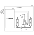
- Embodiment 2. 7 is a diagram showing a configuration example of an air conditioner 300 according to embodiment 2.
- the air conditioner 300 according to embodiment 2 is an example of a refrigeration cycle applied device, and includes a motor drive device 100 and a motor 120 according to embodiment 2.
- the air conditioner 300 also includes a compressor 81, a four-way valve 82, an outdoor heat exchanger 83, an expansion valve 84, an indoor heat exchanger 85, and a refrigerant piping 86.
- the air conditioner 300 may be a separate type air conditioner in which the outdoor unit is separated from the indoor unit, or it may be an integrated type air conditioner in which the compressor 81, indoor heat exchanger 85, and outdoor heat exchanger 83 are provided in a single housing.
- a compression mechanism 87 that compresses the refrigerant
- a motor 120 that operates the compression mechanism 87.
- the motor 120 is driven by a motor drive device 100.
- a refrigeration cycle is formed by circulating the refrigerant through the compressor 81, four-way valve 82, outdoor heat exchanger 83, expansion valve 84, indoor heat exchanger 85, and refrigerant piping 86.
- the components of the air conditioner 300 can also be applied to devices such as refrigerators or freezers equipped with a refrigeration cycle.
- the motor 120 is used as the drive source for the compressor 81, but the motor 120 may also be used as the drive source for driving an indoor unit blower and an outdoor unit blower (not shown) instead of the compressor 81.
- the motor 120 may be used as the drive source for each of the indoor unit blower, the outdoor unit blower, and the compressor 81, and the three motors 120 may be driven by the motor drive device 100.
- the air conditioner 300 according to the second embodiment is configured with the motor drive device 100 according to the first embodiment, so that it is possible to suppress harmonic currents while preventing the converter from becoming large. This makes it possible to provide a product that is inexpensive and does not become large.
Landscapes
- Engineering & Computer Science (AREA)
- Power Engineering (AREA)
- Inverter Devices (AREA)
Priority Applications (2)
| Application Number | Priority Date | Filing Date | Title |
|---|---|---|---|
| JP2025529353A JPWO2025004324A1 (https=) | 2023-06-30 | 2023-06-30 | |
| PCT/JP2023/024379 WO2025004324A1 (ja) | 2023-06-30 | 2023-06-30 | 電力変換装置、モータ駆動装置及び冷凍サイクル適用機器 |
Applications Claiming Priority (1)
| Application Number | Priority Date | Filing Date | Title |
|---|---|---|---|
| PCT/JP2023/024379 WO2025004324A1 (ja) | 2023-06-30 | 2023-06-30 | 電力変換装置、モータ駆動装置及び冷凍サイクル適用機器 |
Publications (1)
| Publication Number | Publication Date |
|---|---|
| WO2025004324A1 true WO2025004324A1 (ja) | 2025-01-02 |
Family
ID=93938063
Family Applications (1)
| Application Number | Title | Priority Date | Filing Date |
|---|---|---|---|
| PCT/JP2023/024379 Ceased WO2025004324A1 (ja) | 2023-06-30 | 2023-06-30 | 電力変換装置、モータ駆動装置及び冷凍サイクル適用機器 |
Country Status (2)
| Country | Link |
|---|---|
| JP (1) | JPWO2025004324A1 (https=) |
| WO (1) | WO2025004324A1 (https=) |
Citations (3)
| Publication number | Priority date | Publication date | Assignee | Title |
|---|---|---|---|---|
| JP2006014497A (ja) * | 2004-06-25 | 2006-01-12 | Daikin Ind Ltd | アクティブコンバータ及びその制御方法 |
| JP2016220378A (ja) * | 2015-05-19 | 2016-12-22 | ジョンソンコントロールズ ヒタチ エア コンディショニング テクノロジー(ホンコン)リミテッド | 直流電源装置、並びにそれを用いる空気調和機 |
| JP2019146348A (ja) * | 2018-02-20 | 2019-08-29 | ファナック株式会社 | Dcリンク部のコンデンサの短絡判定部を有するモータ駆動装置 |
-
2023
- 2023-06-30 JP JP2025529353A patent/JPWO2025004324A1/ja active Pending
- 2023-06-30 WO PCT/JP2023/024379 patent/WO2025004324A1/ja not_active Ceased
Patent Citations (3)
| Publication number | Priority date | Publication date | Assignee | Title |
|---|---|---|---|---|
| JP2006014497A (ja) * | 2004-06-25 | 2006-01-12 | Daikin Ind Ltd | アクティブコンバータ及びその制御方法 |
| JP2016220378A (ja) * | 2015-05-19 | 2016-12-22 | ジョンソンコントロールズ ヒタチ エア コンディショニング テクノロジー(ホンコン)リミテッド | 直流電源装置、並びにそれを用いる空気調和機 |
| JP2019146348A (ja) * | 2018-02-20 | 2019-08-29 | ファナック株式会社 | Dcリンク部のコンデンサの短絡判定部を有するモータ駆動装置 |
Also Published As
| Publication number | Publication date |
|---|---|
| JPWO2025004324A1 (https=) | 2025-01-02 |
Similar Documents
| Publication | Publication Date | Title |
|---|---|---|
| KR920011090B1 (ko) | 공기조화 장치용 교류 전원장치 | |
| CN109937531B (zh) | 电力转换装置及冷冻空调机器 | |
| JP7459308B2 (ja) | 電力変換装置、モータ駆動装置及び冷凍サイクル適用機器 | |
| JP7345673B2 (ja) | 電力変換装置、モータ駆動装置および冷凍サイクル適用機器 | |
| JP7341359B2 (ja) | 電力変換装置、モータ駆動装置及び冷凍サイクル適用機器 | |
| JP7045529B2 (ja) | 電力変換装置および空気調和機 | |
| JP7483055B2 (ja) | 電力変換装置および空気調和機 | |
| WO2025004324A1 (ja) | 電力変換装置、モータ駆動装置及び冷凍サイクル適用機器 | |
| JP6689688B2 (ja) | 電力変換装置、空気調和機および電力変換装置の制御方法 | |
| US20240063708A1 (en) | Power converter, motor driving apparatus, and refrigeration cycle applied apparatus | |
| WO2022176015A1 (ja) | 電力変換装置および空気調和機 | |
| WO2025004325A1 (ja) | 電力変換装置、モータ駆動装置及び冷凍サイクル適用機器 | |
| JP6775548B2 (ja) | モータ制御装置、および、空気調和機 | |
| WO2020183553A1 (ja) | 直流電源装置、電力変換装置及び冷凍サイクル装置 | |
| WO2025004326A1 (ja) | 電力変換装置、モータ駆動装置及び冷凍サイクル適用機器 | |
| JP7278497B2 (ja) | 電力変換装置および空気調和機 | |
| JP7825796B1 (ja) | 電力変換装置及び冷凍サイクル適用機器 | |
| JPWO2020170302A1 (ja) | 電動機駆動装置および空気調和装置 | |
| JP7471505B2 (ja) | 交流直流変換装置、電動機駆動装置及び冷凍サイクル機器 | |
| AU2021417065B2 (en) | Power conversion device, motor driving device, and refrigeration-cycle application device | |
| JP7471991B2 (ja) | 電力変換装置 | |
| JP7166449B2 (ja) | モータ駆動装置、送風機、圧縮機及び空気調和機 | |
| CN117792138A (zh) | 电力转换系统以及制冷循环装置 | |
| WO2018043258A1 (ja) | 電力変換装置及びこれを備える空気調和機 | |
| WO2023238301A1 (ja) | 電力変換装置、モータ駆動装置及びヒートポンプ装置 |
Legal Events
| Date | Code | Title | Description |
|---|---|---|---|
| 121 | Ep: the epo has been informed by wipo that ep was designated in this application |
Ref document number: 23943713 Country of ref document: EP Kind code of ref document: A1 |
|
| ENP | Entry into the national phase |
Ref document number: 2025529353 Country of ref document: JP Kind code of ref document: A |
|
| WWE | Wipo information: entry into national phase |
Ref document number: 2025529353 Country of ref document: JP |
|
| NENP | Non-entry into the national phase |
Ref country code: DE |