WO2024262001A1 - 電子線応用装置 - Google Patents
電子線応用装置 Download PDFInfo
- Publication number
- WO2024262001A1 WO2024262001A1 PCT/JP2023/023303 JP2023023303W WO2024262001A1 WO 2024262001 A1 WO2024262001 A1 WO 2024262001A1 JP 2023023303 W JP2023023303 W JP 2023023303W WO 2024262001 A1 WO2024262001 A1 WO 2024262001A1
- Authority
- WO
- WIPO (PCT)
- Prior art keywords
- surface cleaning
- electron beam
- hydrogen
- electron
- generating means
- Prior art date
- Legal status (The legal status is an assumption and is not a legal conclusion. Google has not performed a legal analysis and makes no representation as to the accuracy of the status listed.)
- Ceased
Links
Images





Classifications
-
- H—ELECTRICITY
- H01—ELECTRIC ELEMENTS
- H01J—ELECTRIC DISCHARGE TUBES OR DISCHARGE LAMPS
- H01J1/00—Details of electrodes, of magnetic control means, of screens, or of the mounting or spacing thereof, common to two or more basic types of discharge tubes or lamps
- H01J1/02—Main electrodes
- H01J1/34—Photo-emissive cathodes
-
- H—ELECTRICITY
- H01—ELECTRIC ELEMENTS
- H01J—ELECTRIC DISCHARGE TUBES OR DISCHARGE LAMPS
- H01J37/00—Discharge tubes with provision for introducing objects or material to be exposed to the discharge, e.g. for the purpose of examination or processing thereof
- H01J37/02—Details
- H01J37/04—Arrangements of electrodes and associated parts for generating or controlling the discharge, e.g. electron-optical arrangement or ion-optical arrangement
- H01J37/06—Electron sources; Electron guns
- H01J37/073—Electron guns using field emission, photo emission, or secondary emission electron sources
Definitions
- the present invention relates to electron beam application devices such as electron microscopes.
- an electron source that is bright and emits an electron beam with a narrow energy range i.e., monochromatic
- Photoexcitation electron sources that utilize negative electron affinity (NEA) have the advantage of having an extremely narrow energy range and monochromaticity that surpasses previous high-performance electron sources, as well as being highly bright.
- short-pulse electron beams can be easily obtained by pulsing the excitation light, making them useful for measuring time resolution.
- the photocathode that emits the electron beam in this photoexcited electron gun has a GaAs surface, and a process called NEA activation (surface activation) is used to create a low work function surface by adsorbing Cs and oxygen to the GaAs surface of the photocathode.
- NEA activation surface activation
- a surface cleaning process is essential to remove oxides and carbides that form on the surface due to gas adsorption in the initial state immediately after insertion of the photocathode into the electron gun and during operation inside the electron gun.
- it is effective to heat the photocathode and irradiate the surface with atomic hydrogen, which is made by dissociating hydrogen molecules.
- Hydrogen is introduced for this purpose by manually operating a variable leak valve to reduce the pressure of hydrogen gas contained in a hydrogen cylinder and introducing it, as shown in Patent Document 1.
- Patent Document 2 discloses a method for reducing and removing adsorbed carbon on the surface of a needle-shaped electron source by irradiating it with atomic hydrogen, and also discloses a method for introducing hydrogen, in which hydrogen is generated by heating a hydrogen storage alloy, and a method for heating a hydrogen-permeable membrane such as Pd that is inserted between a vessel containing hydrogen and a vacuum chamber.
- the electron beam application device which is one embodiment of the present invention, comprises a photocathode with a photoelectric film, a cathode heater for heating the photocathode, atomic hydrogen generating means for dissociating hydrogen molecules to generate atomic hydrogen, control means for controlling the surface cleaning of the surface of the photoelectric film, and measurement means for measuring the probe value of the electron beam probe emitted from the photocathode, and is characterized in that when the probe value measured by the measurement means falls below a predetermined value, the control means determines the surface cleaning conditions for the photoelectric film, controls the cathode heater and the atomic hydrogen generating means under the determined surface cleaning conditions, and performs surface cleaning of the surface of the photoelectric film.
- the surface cleaning of photocathodes and needle-shaped cathodes can be performed automatically in a short time with good reproducibility and without the need for skill, making it possible to form an electron gun that can obtain a stable probe current for a long period of time, resulting in an easy-to-use electron beam application device.
- FIG. 1 is a schematic diagram of an electron beam application device using a photoexcited electron gun according to a first embodiment of the present invention.
- FIG. 2 is a time chart showing the operation of each component during surface cleaning according to the first embodiment of the present invention.
- 1 is a flow chart of an automatic surface cleaning method according to a first embodiment of the present invention.
- FIG. 4 is a history diagram of a probe current value (Ip) according to the first embodiment of the present invention. 4 is a flowchart of an operation of an electron beam application device using a photoexcited electron gun according to the first embodiment of the present invention.
- 2 is an example of a hydrogen generating means according to a first embodiment of the present invention.
- 2 is an example of a hydrogen generating means according to a first embodiment of the present invention.
- FIG. 2 is an example of a hydrogen generating means according to a first embodiment of the present invention.
- FIG. 11 is a schematic diagram of an electron beam application device using a needle-shaped electron source according to a second embodiment of the present invention. 10 is a flowchart of an operation of an electron beam application device using a needle-shaped electron source according to a second embodiment of the present invention.
- FIG. 11 is a schematic diagram of an electron beam application device using a needle-shaped electron source according to a third embodiment of the present invention. 1 shows an example of a hydrogen generating means according to embodiments 1 to 3 of the present invention.
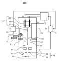
- FIG. 1A is a schematic diagram of an electron beam application device using a photoexcited electron gun according to Example 1 of the present invention.
- the photocathode 1 is a transmission type photocathode with a structure in which a photoelectric film 10 is provided on the surface of a transparent substrate 11, and the electron beam emission surface and the excitation light incidence surface are opposite.
- the photocathode 1 can take two positions, an electron gun position on the right side in FIG. 1A and a surface cleaning position on the left side, by a linear introducer 17.
- the photoelectric film 10 is made of a material mainly consisting of single crystal GaAs as described in Patent Document 1, and is a monochromatic electron beam emission source with high brightness and uniform energy that utilizes negative electron affinity (NEA) by making the surface a low work function and irradiating excitation light from the back.
- NAA negative electron affinity
- the photoelectric film 10 When the photocathode 1 is at the electron gun position, the photoelectric film 10, whose surface has a low work function due to Cs and oxygen, is irradiated with excitation light 21 generated from a laser light source 22 by instructions from the electron gun controller 19 through a window 23 at the top of the vacuum vessel 29 and onto a small area by a condenser lens 20.
- the electrons emitted as a result are accelerated between the extraction electrode 26 and become an electron beam probe 27, which passes from the electron gun 15 through an aperture 28 and enters the electron optical system column 30 and is used as a microscope.
- the electron optical component 52 controls an electron beam probe 27 consisting of an electron lens, a deflector, etc.
- the various elements in the electron optical system column 30, namely the secondary electron detector 51, the electron optical component 52, the sample 50, and the electron gun controller 19 controlled by the system control device 8, function as an electron microscope that uses the electron beam probe 27 to observe the microstructure of the surface of the sample 50.
- This electron optical system column 30 is typically used as a scanning electron microscope (SEM), a transmission electron microscope (TEM), etc.
- the energy of the electron beam probe 27 is determined by the potential of the photocathode 1.
- the photocathode 1 has electrical contact with a cathode contact (not shown), and an acceleration voltage (V0) is applied to it from an external power supply (not shown) in response to instructions from the electron gun controller 19.
- the energy of the electron beam probe 27 is determined by this acceleration voltage (V0).
- the emission current emitted from the photocathode 1 is monitored on the power supply side.
- a probe current measuring means 18 is arranged within the electron optical system column 30, which monitors the probe current value (Ip) of the electron beam probe 27 and communicates that value to the system control device 8.
- the probe current measuring means 18 is composed of, for example, an aperture 39 and a current detector 38, and measures the current caused by electrons irradiating the aperture 39 with the part of the electron beam probe 27 that spreads out from the center of the orbit.
- the work function of the surface of the photoelectric film 10 is reduced by depositing Cs by electrically heating the Cs source 9 and introducing oxygen gas by the oxygen generating means 5, which is called the surface activation process. These processes are controlled automatically by electrical signals from the surface controller 7.
- the photocathode 1 is placed at the surface cleaning position by the linear introducer 17, and the removal of oxides and carbides by atomic hydrogen is automated.
- the surface cleaning configuration consists of the cathode heater 2, atomic hydrogen generator 4, hydrogen generating means 3, and heating element (hydrogen heater) 6 in FIG. 1A, which are operated by electrical signals from the surface controller 7.
- FIG. 1B is a time-lapse diagram of the operation of each component during surface cleaning according to the first embodiment of the present invention.
- the cathode heater 2 is energized to heat the photocathode 1 to a temperature (Tc) of 400°C to 500°C.
- the hydrogen generating means 3 generates hydrogen by heating, and is heated to the H2 source temperature (Th2) by the heating element (hydrogen heater) 6 so as to achieve the desired pressure. As a result, the gas pressure (P) inside the electron gun increases.
- the W filament (HC (Hydrogen cracking) heater) of the atomic hydrogen generator 4 is energized to heat it to the HC heater temperature (Thc), dissociating the hydrogen molecules to generate highly reactive atomic hydrogen.
- This HC heater temperature is selected from the range of 1800°C to 2000°C. This state is maintained for an automatically determined surface cleaning time (tcl), after which each current value is stopped and both the temperature and pressure return to their original values.
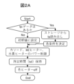
- 2A is a flow chart of automatic surface cleaning according to the first embodiment of the present invention. This process is mainly performed by signals from the surface controller 7. First, since the conditions vary depending on the history of the surface of the photocathode 1, if there is a probe current value (Ip) measured under standard conditions when the emission current increases due to activation or Cs addition, the surface cleaning conditions are determined by the history of this probe current value (Ip).
- the history of the probe current value (Ip) is a record of the probe current value (Ip) after activation or Cs addition, and in this embodiment, it is stored in the storage of the system control device 8.
- the probe current value (Ip) varies depending on the acceleration voltage (V0) and the intensity of the excitation light 21, so it is determined by measuring the current value under a constant acceleration and a constant excitation light intensity, i.e., standard conditions.
- the probe current value (Ip) measured under that condition may be converted to the acceleration voltage and excitation light intensity under standard conditions and used.
- the conversion can be done from the emission current value from the photocathode 1. If the photocathode 1 is new and there is no measured probe current value (Ip), the surface cleaning conditions are set to the initial values.
- the power to the cathode heater 2, HC heater (W filament of the atomic hydrogen generator 4), and heating element (hydrogen heater) 6 is controlled to achieve the set surface cleaning conditions, which are maintained for the set specified time (tcl), after which the power to each heater is stopped and the process is completed.
- the surface cleaning conditions are determined as follows. In the case of a brand new photocathode 1 with a protective film formed on the surface in a crystal growth apparatus, a clean surface can be obtained with light surface cleaning.
- the surface cleaning conditions in this case are, for example, hydrogen pressure (P): 1 x 10 ⁇ -4 Pa, HC heater temperature (Thc): 1800°C, cathode temperature (Tc): 400°C, surface cleaning time (tcl): 10 to 20 minutes [Condition 1].
- FIG. 2B is a history diagram of the probe current value (Ip) according to the first embodiment of the present invention.
- the probe current value (Ip) After replacing the photocathode 1, if the surface of the photoelectric film 10 is only slightly dirty, the probe current value (Ip) will hardly change even if activation or Cs addition is performed. This region is indicated by A in FIG. 2B. If the surface of the photoelectric film 10 becomes slightly dirty with oxides or carbides, the probe current value (Ip) will gradually decrease even if activation or Cs addition is performed. This region is indicated by B in FIG. 2B. Furthermore, when a sample containing a large amount of gas is observed in the electron optical system column 30, the probe current value (Ip) will decrease rapidly. This region is indicated by C in FIG. 2B. If the probe current value (Ip) falls below a predetermined value (Ic), it is determined that surface cleaning is necessary.
- Ic predetermined value
- the surface cleaning conditions are, for example, hydrogen pressure (P): 2 x 10 ⁇ -4 Pa, HC heater temperature (Thc): 1900°C, cathode temperature (Tc): 400°C, and surface cleaning time (tcl): 20 minutes [Condition 2].
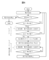
- FIG. 3 is a flow chart of the operation of an electron beam application device using a photoexcited electron gun according to the first embodiment of the present invention.
- the photocathode 1 is moved to the surface cleaning position. This is performed by applying an electrical signal from the surface controller 7 to the power of the linear introducer 17.
- the automatic surface cleaning process shown in FIG. 2A is performed. If the photocathode 1 is new, the surface of the photoelectric film 10 is first cleaned under the above-mentioned [Condition 1].
- the photocathode 1 is moved to the electron gun position by the linear introducer 17, and surface activation is performed on the surface of the photoelectric film 10 using Cs and oxygen.
- Electron beam emission is performed by irradiating the photocathode 1 with excitation light 21. After this, a predetermined acceleration voltage (V0) is applied to the photocathode 1 to emit an electron beam, and an electron beam probe 27 is generated.
- the probe current measurement means 18 of the electron optical system column 30 measures the probe current value (Ip) at any time or continuously, and if it is equal to or greater than a predetermined value, the electron beam emission is continued and sample observation is performed.
- the electron beam is stopped and the measurement is terminated. If the probe current value (Ip) decreases while the measurement is continuing, power is applied to the Cs source 9 and Cs is added. If this causes the probe current value (Ip) to recover to a specified value or higher, the electron beam emission is continued. If the probe current value (Ip) does not reach the specified value, surface cleaning is required. In this case, electron emission must be interrupted, so the GUI display on the display of the electron beam application device indicates that surface cleaning (cleaning) is required. If image acquisition is in progress, this is simply displayed continuously. After image acquisition is completed, the electron beam is stopped, and if the measurement is not completed, the photocathode 1 is moved to the surface cleaning position and automatic surface cleaning is performed.
- the surface controller 7 calls up the historical data of the probe current value (Ip) from the storage of the system control device 8 as shown in Figure 2A, and referring to the decrease pattern as shown in Figure 2B, selects the aforementioned [Condition 1], [Condition 2], [Condition 3] or intermediate conditions to perform automatic surface cleaning. Due to the system configuration, this selection is performed by the system control device 8, and the same effect can be achieved by communicating the result to the surface controller 7.
- FIG. 4A shows an example of the hydrogen generation means 3.
- a cylindrical hydrogen storage alloy 12 with a hole in the center is provided as the hydrogen generation means 3 in the vacuum in which the electron gun 15 is provided inside the vacuum vessel 29.
- the heating element (hydrogen heater) 6 is inserted into the hole in the hydrogen storage alloy 12 from the atmosphere side outside the vacuum vessel 29, and electricity is passed through the wiring 13 of the heating element (hydrogen heater) 6 to raise the temperature of the hydrogen storage alloy 12 and generate hydrogen.
- the H2 source temperature (Th2) may be determined in advance by measuring the hydrogen pressure so as to generate the desired hydrogen pressure (P). In that case, it can be reproduced by simple conditions such as the power or current value of the heating element (hydrogen heater) 6.
- a non-evaporative getter material may be used as the hydrogen storage alloy 12.
- a cartridge heater or the like is used as the heating element (hydrogen heater) 6.
- the H2 source temperature (Th2) varies depending on the type and amount of alloy, but is selected from the range of 200°C to 700°C.
- the heating element (hydrogen heater) 6 is in contact with the hydrogen storage alloy 12 in the vacuum of the vacuum vessel 29 as shown in FIG. 4B.
- the wiring 13 of the heating element (hydrogen heater) 6 is drawn to the outside of the vacuum vessel 29 by the feedthrough 14.
- an aluminum or magnesium hydride is used as the hydrogen generating means 3 and hydrogen is generated by heating and thermal decomposition.
- a gas container 24 may be filled with a gas containing hydrogen, and connected to a vacuum container 29 in which an electron gun 15 is provided via vacuum piping 16 separated by a hydrogen permeable membrane 25, and the hydrogen permeable membrane 25 may be heated by a heating element (hydrogen heater) 6.
- a heating element hydrogen heater
- Metals such as Pd, Ta, Nb, and V are used as the hydrogen permeable membrane 25.
- the H2 source temperature (Th2) is the heating temperature of the hydrogen permeable membrane 25, and is selected from the range of approximately 150°C to 300°C.
- Hydrogen permeable membrane 25 often has good hydrogen permeability at around 200°C, so when it is desired to control the gas pressure at temperatures higher than 200°C and when considering safety in case of gas leakage, it is easier to use the gas filled in gas container 24 if it is diluted with an inert gas such as Ar rather than 100% hydrogen.
- the degree of dilution is selected, for example, from about 10 to 10,000 volumes of inert gas per volume of hydrogen.
- the linear introducer 17 moves the position of the photocathode 1 using an electrical signal, and is powered by conventional means such as compressed air or a motor.
- the linear introducer 17 can also be manually repositioned so that the position of the photocathode 1 can be changed according to instructions on the GUI display on the display of the electron beam application device, which can be easily performed without requiring the operator to be highly skilled, resulting in a similar effect of providing an easy-to-use electron beam application device.
- an electron beam application device that uses a photoexcited electron source that uses a photocathode for the electron gun
- surface cleaning to prevent instability in the probe current can be automated, so that anyone can use the electron gun in an easy-to-use manner, and samples can be observed stably for long periods of time in an electron beam application device that uses this.
- the extraction electrode 26 facing the FE electron source 37 is fixed to the vacuum vessel 29 by an insulator 35 and is electrically connected to the electron source controller 34.
- the vacuum vessel 29 housing the FE electron source 37 is kept in an ultra-high vacuum range by a vacuum pump (not shown).
- an atomic hydrogen generator 4 as a means for generating atomic hydrogen, hydrogen generating means 3, a heating element (hydrogen heater) 6, and an atomic hydrogen controller 36 are provided.
- the conventional method of use is to heat the needle-shaped metal 31 to over 2000°C before generating the electron beam to remove oxides and carbides adhering to the surface.
- a process called flashing is performed in which electricity is momentarily passed between each electrode (F1, F2) to heat the filament 32 to a high temperature and heat the needle-shaped metal 31.
- an acceleration voltage (V0) is applied to each electrode (F1, F2) and an extraction voltage is applied to the extraction electrode 26, and the electrons emitted from the needle-shaped metal 31 are guided to the electron optical system column 30 as the electron beam probe 27 and used to observe the sample 50.
- FIG. 6 is a flow chart of the operation of an electron beam application device using a needle-shaped electron source according to the second embodiment of the present invention.
- atomic hydrogen generating means (3, 4, 6) and an atomic hydrogen controller 36 are arranged, and the device is automatically operated in a high brightness state.
- FIG. 6 shows an example of operation after high-temperature flashing, in which electron emission is started and SEM observation is performed. When the SEM measurement is completed, electron emission is stopped and the device is terminated. The end of the measurement is determined by the user or the system control device performing the automatic measurement.
- the probe current value (Ip) is monitored at any time by the probe current measuring means 18, and if it is equal to or greater than the specified value, the measurement is continued.
- the needle-shaped metal 31 is heated to about 1000°C or less in a short time, and if the probe current value (Ip) recovers, electron emission is continued and SEM observation is continued. This is the same as the conventional mild flashing process.
- the SEM system control device 8 displays a GUI display indicating that surface cleaning is required, and the atomic hydrogen controller 36 issues a signal to raise the H2 source temperature (Th2) of the heating element (hydrogen heater) 6 of the hydrogen generating means 3 and the HC heater temperature (Thc) of the W filament (HC heater) of the atomic hydrogen generator 4 to generate atomic hydrogen.
- electricity is instantly passed between the electrodes (F1, F2) to heat the filament 32 to a high temperature, and the needle-shaped metal 31 is heated to a temperature of about 1000°C or less for a short period of time under the same conditions as mild flashing.
- This process is carried out until the probe current value (Ip) recovers to a predetermined value, and after recovery, electricity is stopped from passing through the heating element (hydrogen heater) 6 and the W filament (HC heater) of the atomic hydrogen generator 4, and the atomic hydrogen is stopped. This removes surface carbides, returns the tip surface of the needle-shaped metal 31 to its original state, and SEM observation is continued.
- FIG. 7 is a schematic diagram of an electron beam application device using a needle-shaped electron source according to a third embodiment of the present invention.
- the electron gun 15 is configured with an electron source chamber 40 housing the electron source and a differential pumping chamber 41, atomic hydrogen is generated in the differential pumping chamber 41, and atomic hydrogen is supplied to the electron source chamber 40 via an aperture 28 between the electron source chamber 40 and the differential pumping chamber 41.
- the flow of FIG. 6 of the second embodiment can also provide the same effect, but in the third embodiment, the amount of atomic hydrogen entering the electron source chamber 40 is significantly reduced compared to the atomic hydrogen released from the atomic hydrogen generator 4, so it is advisable to increase the amount of hydrogen supplied.
- atomic hydrogen can be generated for a long period of time, rather than instantaneously, and the FE electron source 37 can be mildly flushed during that time to remove the gas adsorbed on the surface, so that a probe current value (Ip) that is stable for a long period of time can also be obtained.
- Ip probe current value
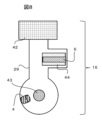
- FIG. 8 is a schematic diagram of the cross-sectional structure of the electron gun 15 seen from above.
- the electron source part 43 is located in the center of a cylindrical container, and the vacuum container 29 is evacuated by ion pumps 42 and non-evaporative getter pumps 44 arranged in the peripheral parts to maintain an ultra-high vacuum.
- the non-evaporative getter pump 44 is normally operated at room temperature, but generates hydrogen by heating it with a heating element (hydrogen heater) 6.
- This hydrogen spreads in the vacuum container 29 in which the electron gun 15 is provided, and atomic hydrogen is generated by the atomic hydrogen generator 4 placed separately near the electron source part 43, which can be used to clean the surface of the electron source, and the same effect as in the first to third embodiments can be obtained.
- a hydrogen cracking heater (HC heater) with a high-temperature W filament was used as the atomic hydrogen generator 4, but any means for dissociating hydrogen molecules will have a similar effect, and for example, atomic hydrogen dissociated by turning hydrogen gas into plasma may be used. It is well known that plasma can be generated by applying high voltage or high frequency, irradiating with laser light, etc.
- a needle-shaped metal 31 made of W is used as the FE electron source 37, but other high-brightness electron sources are also sensitive to surface contamination, so similar effects can be obtained by applying this invention.
- a similar effect can be obtained in an SE (Schottky emission) electron source in which Zr-O is adsorbed onto a W (100) surface and heated, or in the case of using a high-melting-point conductor such as a metal hexaboride or metal carbide, represented by CeB6, as the needle-shaped metal 31.
- a high-melting-point conductor such as a metal hexaboride or metal carbide, represented by CeB6, as the needle-shaped metal 31.
- long-term stabilization can be achieved by adjusting the probe current value (Ip) so that atomic hydrogen is generated intermittently or continuously.
Landscapes
- Chemical & Material Sciences (AREA)
- Analytical Chemistry (AREA)
- Electron Sources, Ion Sources (AREA)
Abstract
Description
Claims (13)
- 光電膜を備えたフォトカソードと、前記フォトカソードを加熱するカソードヒーターと、水素分子を解離させ原子状水素を発生する原子状水素発生手段と、前記光電膜の表面の表面清浄化を制御する制御手段と、前記フォトカソードから放出された電子線プローブのプローブ値を計測する計測手段と、を備え、
前記計測手段で計測されたプローブ値が所定値を下回った場合に、前記制御手段が、前記光電膜の表面清浄化条件を決定し、前記カソードヒーターと前記原子状水素発生手段を決定した表面清浄化条件で制御し、前記光電膜の表面の表面清浄化を行うことを特徴とする電子線応用装置。 - 前記制御手段が、前記計測手段で計測されたプローブ値の履歴に基づいて前記光電膜の表面清浄化条件を決定することを特徴とする請求項1に記載の電子線応用装置。
- さらに、水素分子を発生する水素発生手段と、前記水素発生手段を加熱する水素ヒーターと、を備え、
前記制御手段が、前記水素ヒーターを決定した表面清浄化条件で制御することを特徴とする請求項2に記載の電子線応用装置。 - さらに、ディスプレーを備え、
前記光電膜の表面の表面清浄化を行う前に、前記ディスプレーにGUI表示で表面清浄化が必要であることを表示することを特徴とする請求項2に記載の電子線応用装置。 - 前記フォトカソードを収めた電子源室と、差動排気室と、を有し、
前記原子状水素発生手段が前記差動排気室に設けられ、前記電子源室と前記差動排気室の間のアパーチャを介して前記電子源室に原子状水素を供給することを特徴とする請求項2に記載の電子線応用装置。 - さらに、Cs源を備え、
前記Cs源によるCs追加を行っても前記計測手段で計測されたプローブ値が所定値以上に回復しない場合に、前記光電膜の表面の表面清浄化を行うことを特徴とする請求項2に記載の電子線応用装置。 - 前記原子状水素発生手段と前記水素発生手段を別置きとし、前記原子状水素発生手段を前記フォトカソードの近くに設けたことを特徴とする請求項3に記載の電子線応用装置。
- 針状金属と、前記針状金属を加熱するフィラメントと、水素分子を解離させ原子状水素を発生する原子状水素発生手段と、前記針状金属の表面の表面清浄化を制御する制御手段と、前記針状金属から放出された電子線プローブのプローブ値を計測する計測手段と、を備え、
前記計測手段で計測されたプローブ値が所定値を下回った場合に、前記制御手段が、前記針状金属の表面清浄化条件を決定し、前記フィラメントと前記原子状水素発生手段を決定した表面清浄化条件で制御し、前記針状金属の表面の表面清浄化を行うことを特徴とする電子線応用装置。 - 前記制御手段が、前記計測手段で計測されたプローブ値の履歴に基づいて前記針状金属の表面清浄化条件を決定することを特徴とする請求項8に記載の電子線応用装置。
- さらに、水素分子を発生する水素発生手段と、前記水素発生手段を加熱する水素ヒーターと、を備え、
前記制御手段が、前記水素ヒーターを決定した表面清浄化条件で制御することを特徴とする請求項9に記載の電子線応用装置。 - さらに、ディスプレーを備え、
前記針状金属の表面の表面清浄化を行う前に、前記ディスプレーにGUI表示で表面清浄化が必要であることを表示することを特徴とする請求項9に記載の電子線応用装置。 - 前記針状金属を収めた電子源室と、差動排気室と、を有し、
前記原子状水素発生手段が前記差動排気室に設けられ、前記電子源室と前記差動排気室の間のアパーチャを介して前記電子源室に原子状水素を供給することを特徴とする請求項9に記載の電子線応用装置。 - 前記原子状水素発生手段と前記水素発生手段を別置きとし、前記原子状水素発生手段を前記針状金属の近くに設けたことを特徴とする請求項10に記載の電子線応用装置。
Priority Applications (2)
| Application Number | Priority Date | Filing Date | Title |
|---|---|---|---|
| JP2025527378A JPWO2024262001A1 (ja) | 2023-06-23 | 2023-06-23 | |
| PCT/JP2023/023303 WO2024262001A1 (ja) | 2023-06-23 | 2023-06-23 | 電子線応用装置 |
Applications Claiming Priority (1)
| Application Number | Priority Date | Filing Date | Title |
|---|---|---|---|
| PCT/JP2023/023303 WO2024262001A1 (ja) | 2023-06-23 | 2023-06-23 | 電子線応用装置 |
Publications (1)
| Publication Number | Publication Date |
|---|---|
| WO2024262001A1 true WO2024262001A1 (ja) | 2024-12-26 |
Family
ID=93935019
Family Applications (1)
| Application Number | Title | Priority Date | Filing Date |
|---|---|---|---|
| PCT/JP2023/023303 Ceased WO2024262001A1 (ja) | 2023-06-23 | 2023-06-23 | 電子線応用装置 |
Country Status (2)
| Country | Link |
|---|---|
| JP (1) | JPWO2024262001A1 (ja) |
| WO (1) | WO2024262001A1 (ja) |
Cited By (1)
| Publication number | Priority date | Publication date | Assignee | Title |
|---|---|---|---|---|
| US20230335367A1 (en) * | 2020-11-10 | 2023-10-19 | Hitachi High-Tech Corporation | Electron beam application device |
Citations (5)
| Publication number | Priority date | Publication date | Assignee | Title |
|---|---|---|---|---|
| JP2002313273A (ja) * | 2001-04-17 | 2002-10-25 | Hitachi Ltd | 電子顕微鏡装置 |
| JP2007172862A (ja) * | 2005-12-19 | 2007-07-05 | Hitachi High-Technologies Corp | 荷電粒子線源用清浄化装置及びそれを用いた荷電粒子線装置 |
| JP2011171088A (ja) * | 2010-02-18 | 2011-09-01 | Hitachi High-Technologies Corp | 電界放出電子銃及びその制御方法 |
| US20200088660A1 (en) * | 2016-12-23 | 2020-03-19 | Orion Engineering Limited | Handheld material analyser |
| WO2022101957A1 (ja) * | 2020-11-10 | 2022-05-19 | 株式会社日立ハイテク | 電子線応用装置 |
-
2023
- 2023-06-23 WO PCT/JP2023/023303 patent/WO2024262001A1/ja not_active Ceased
- 2023-06-23 JP JP2025527378A patent/JPWO2024262001A1/ja active Pending
Patent Citations (5)
| Publication number | Priority date | Publication date | Assignee | Title |
|---|---|---|---|---|
| JP2002313273A (ja) * | 2001-04-17 | 2002-10-25 | Hitachi Ltd | 電子顕微鏡装置 |
| JP2007172862A (ja) * | 2005-12-19 | 2007-07-05 | Hitachi High-Technologies Corp | 荷電粒子線源用清浄化装置及びそれを用いた荷電粒子線装置 |
| JP2011171088A (ja) * | 2010-02-18 | 2011-09-01 | Hitachi High-Technologies Corp | 電界放出電子銃及びその制御方法 |
| US20200088660A1 (en) * | 2016-12-23 | 2020-03-19 | Orion Engineering Limited | Handheld material analyser |
| WO2022101957A1 (ja) * | 2020-11-10 | 2022-05-19 | 株式会社日立ハイテク | 電子線応用装置 |
Non-Patent Citations (1)
| Title |
|---|
| MORISHITA, HIDEO ET AL.: "R esolution improvement of low-voltage scanning electron microscope by bright and monochromatic electron gun using negative electron affinity photocathode", JOURNAL OF APPLIED PHYSICS, vol. 127, 2020, pages 1 - 7, XP012246338, DOI: 10.1063/5.0005714 * |
Cited By (2)
| Publication number | Priority date | Publication date | Assignee | Title |
|---|---|---|---|---|
| US20230335367A1 (en) * | 2020-11-10 | 2023-10-19 | Hitachi High-Tech Corporation | Electron beam application device |
| US12437958B2 (en) * | 2020-11-10 | 2025-10-07 | Hitachi High-Tech Corporation | Electron beam application device |
Also Published As
| Publication number | Publication date |
|---|---|
| JPWO2024262001A1 (ja) | 2024-12-26 |
Similar Documents
| Publication | Publication Date | Title |
|---|---|---|
| JP5514472B2 (ja) | 荷電粒子線装置 | |
| US8822945B2 (en) | Focused ion beam apparatus | |
| EP2110843B1 (en) | Stable emission gas ion source and method of operation thereof | |
| JP2007172862A (ja) | 荷電粒子線源用清浄化装置及びそれを用いた荷電粒子線装置 | |
| JP6001292B2 (ja) | エミッタの作製方法 | |
| JP6501891B2 (ja) | イオンビーム装置およびガス電界電離イオン源の洗浄方法 | |
| US6667475B1 (en) | Method and apparatus for cleaning an analytical instrument while operating the analytical instrument | |
| JPWO2018055715A1 (ja) | 電子顕微鏡 | |
| US20080284332A1 (en) | Gun chamber, charged particle beam apparatus and method of operating same | |
| JP2021524650A (ja) | 拡散障壁を有する電子エミッタ向けの金属保護層 | |
| JP6594983B2 (ja) | イオンビーム装置、及び試料元素分析方法 | |
| JP6112930B2 (ja) | ガスイオン源、及び集束イオンビーム装置 | |
| WO2015053300A1 (ja) | 電子顕微鏡 | |
| US10249471B2 (en) | Composite charged particle beam apparatus and control method thereof | |
| JP5432028B2 (ja) | 集束イオンビーム装置、チップ先端構造検査方法及びチップ先端構造再生方法 | |
| JP2019102242A (ja) | 単原子終端構造を有するイオン源および電子源、単原子終端構造を有するティップ、ガス電界電離イオン源、集束イオンビーム装置、電子源、電子顕微鏡、マスク修正装置、並びに単原子終端構造を有するティップの製造方法 | |
| US12437958B2 (en) | Electron beam application device | |
| JP5742059B2 (ja) | 電子発生方法 | |
| Jüttner et al. | Stability of field electron emission and vacuum breakdown. Investigations with field emission microscopy and Auger electron spectroscopy | |
| US2467225A (en) | Reducing specimen contamination in electron optical instruments | |
| CN121123002A (zh) | 一种提高离子源束流强度的方法及其装置 | |
| WO2026009310A1 (ja) | 荷電粒子線装置 | |
| JPH08129981A (ja) | 電界放射型電子銃及び電子線装置 | |
| JP6236480B2 (ja) | エミッタの作製方法 | |
| Maciel et al. | Studies of a hollow cathode discharge using mass spectrometry and electrostatic probe techniques |
Legal Events
| Date | Code | Title | Description |
|---|---|---|---|
| 121 | Ep: the epo has been informed by wipo that ep was designated in this application |
Ref document number: 23942433 Country of ref document: EP Kind code of ref document: A1 |
|
| ENP | Entry into the national phase |
Ref document number: 2025527378 Country of ref document: JP Kind code of ref document: A |
|
| WWE | Wipo information: entry into national phase |
Ref document number: 2025527378 Country of ref document: JP |
|
| NENP | Non-entry into the national phase |
Ref country code: DE |
|
| 122 | Ep: pct application non-entry in european phase |
Ref document number: 23942433 Country of ref document: EP Kind code of ref document: A1 |