WO2024262000A1 - 装置およびその制御方法ならびにプログラム - Google Patents
装置およびその制御方法ならびにプログラム Download PDFInfo
- Publication number
- WO2024262000A1 WO2024262000A1 PCT/JP2023/023295 JP2023023295W WO2024262000A1 WO 2024262000 A1 WO2024262000 A1 WO 2024262000A1 JP 2023023295 W JP2023023295 W JP 2023023295W WO 2024262000 A1 WO2024262000 A1 WO 2024262000A1
- Authority
- WO
- WIPO (PCT)
- Prior art keywords
- scanning
- pixel
- sample
- image
- controller
- Prior art date
- Legal status (The legal status is an assumption and is not a legal conclusion. Google has not performed a legal analysis and makes no representation as to the accuracy of the status listed.)
- Ceased
Links
Images



Classifications
-
- H—ELECTRICITY
- H01—ELECTRIC ELEMENTS
- H01J—ELECTRIC DISCHARGE TUBES OR DISCHARGE LAMPS
- H01J37/00—Discharge tubes with provision for introducing objects or material to be exposed to the discharge, e.g. for the purpose of examination or processing thereof
- H01J37/02—Details
- H01J37/22—Optical, image processing or photographic arrangements associated with the tube
- H01J37/222—Image processing arrangements associated with the tube
-
- G—PHYSICS
- G01—MEASURING; TESTING
- G01N—INVESTIGATING OR ANALYSING MATERIALS BY DETERMINING THEIR CHEMICAL OR PHYSICAL PROPERTIES
- G01N23/00—Investigating or analysing materials by the use of wave or particle radiation, e.g. X-rays or neutrons, not covered by groups G01N3/00 – G01N17/00, G01N21/00 or G01N22/00
- G01N23/22—Investigating or analysing materials by the use of wave or particle radiation, e.g. X-rays or neutrons, not covered by groups G01N3/00 – G01N17/00, G01N21/00 or G01N22/00 by measuring secondary emission from the material
- G01N23/225—Investigating or analysing materials by the use of wave or particle radiation, e.g. X-rays or neutrons, not covered by groups G01N3/00 – G01N17/00, G01N21/00 or G01N22/00 by measuring secondary emission from the material using electron or ion
-
- G—PHYSICS
- G01—MEASURING; TESTING
- G01N—INVESTIGATING OR ANALYSING MATERIALS BY DETERMINING THEIR CHEMICAL OR PHYSICAL PROPERTIES
- G01N23/00—Investigating or analysing materials by the use of wave or particle radiation, e.g. X-rays or neutrons, not covered by groups G01N3/00 – G01N17/00, G01N21/00 or G01N22/00
- G01N23/22—Investigating or analysing materials by the use of wave or particle radiation, e.g. X-rays or neutrons, not covered by groups G01N3/00 – G01N17/00, G01N21/00 or G01N22/00 by measuring secondary emission from the material
- G01N23/225—Investigating or analysing materials by the use of wave or particle radiation, e.g. X-rays or neutrons, not covered by groups G01N3/00 – G01N17/00, G01N21/00 or G01N22/00 by measuring secondary emission from the material using electron or ion
- G01N23/2251—Investigating or analysing materials by the use of wave or particle radiation, e.g. X-rays or neutrons, not covered by groups G01N3/00 – G01N17/00, G01N21/00 or G01N22/00 by measuring secondary emission from the material using electron or ion using incident electron beams, e.g. scanning electron microscopy [SEM]
-
- H—ELECTRICITY
- H01—ELECTRIC ELEMENTS
- H01J—ELECTRIC DISCHARGE TUBES OR DISCHARGE LAMPS
- H01J37/00—Discharge tubes with provision for introducing objects or material to be exposed to the discharge, e.g. for the purpose of examination or processing thereof
- H01J37/02—Details
- H01J37/22—Optical, image processing or photographic arrangements associated with the tube
-
- H—ELECTRICITY
- H01—ELECTRIC ELEMENTS
- H01J—ELECTRIC DISCHARGE TUBES OR DISCHARGE LAMPS
- H01J37/00—Discharge tubes with provision for introducing objects or material to be exposed to the discharge, e.g. for the purpose of examination or processing thereof
- H01J37/02—Details
- H01J37/244—Detectors; Associated components or circuits therefor
-
- H—ELECTRICITY
- H01—ELECTRIC ELEMENTS
- H01J—ELECTRIC DISCHARGE TUBES OR DISCHARGE LAMPS
- H01J37/00—Discharge tubes with provision for introducing objects or material to be exposed to the discharge, e.g. for the purpose of examination or processing thereof
- H01J37/26—Electron or ion microscopes; Electron or ion diffraction tubes
- H01J37/28—Electron or ion microscopes; Electron or ion diffraction tubes with scanning beams
-
- H—ELECTRICITY
- H10—SEMICONDUCTOR DEVICES; ELECTRIC SOLID-STATE DEVICES NOT OTHERWISE PROVIDED FOR
- H10P—GENERIC PROCESSES OR APPARATUS FOR THE MANUFACTURE OR TREATMENT OF DEVICES COVERED BY CLASS H10
- H10P74/00—Testing or measuring during manufacture or treatment of wafers, substrates or devices
-
- H—ELECTRICITY
- H01—ELECTRIC ELEMENTS
- H01J—ELECTRIC DISCHARGE TUBES OR DISCHARGE LAMPS
- H01J2237/00—Discharge tubes exposing object to beam, e.g. for analysis treatment, etching, imaging
- H01J2237/22—Treatment of data
- H01J2237/221—Image processing
Definitions
- the present invention relates to an apparatus, a control method thereof, and a program thereof, for example, an electron beam apparatus and a semiconductor inspection apparatus using the same, and a control method thereof and a program thereof.
- Patent Document 1 shows a scanning electron microscope (hereinafter also referred to as SEM) that scans a sample multiple times with a charged particle beam, detects the emitted electrons, and generates an output image.
- SEM scanning electron microscope
- Patent Document 1 also shows that an image with a uniform brightness level is generated over the entire field of view by normalizing the brightness value of each pixel in the scan area by the irradiation time of the charged particle beam.
- Scanning electron microscopes are used in a wide range of fields, including semiconductor devices, electronics, advanced materials, biology, and pharmaceuticals.
- the Voltage Contrast (hereinafter referred to as VC) method is also used, in which an electron beam is irradiated onto the surface, and the potential contrast caused by the potential difference generated on the charged surface is observed to observe failures and defects.
- the contrast sensitivity decreases, so it takes time to search for optimal scanning parameters, and precise positioning is required during observation, which requires extra steps such as preliminary observation to confirm the validity of the position. It is expected that semiconductors will continue to become finer and more complex in the future, so it is essential to improve the contrast of the VC method, shorten the observation time, and shorten the TAT (turnaround time).
- Patent Document 1 normalizes the cumulative brightness value per unit area of the sample surface by the cumulative electron beam irradiation time for that area when there are areas on the sample where the scanning speed is different or secondary electrons are not easily generated within a single captured image.
- This technology aligns the brightness levels of images of each area with different scanning conditions when the amount of electrons irradiated per unit area differs due to differences in scanning conditions such as scanning speed or overlapping scanning.
- Patent Document 1 only shows that the cumulative electron beam irradiation time is used to normalize the brightness level, and does not recognize the improvement of contrast, shortening of observation time, and shortening of TAT in the VC method.
- Patent Document 1 also does not recognize that captured images are acquired in VC observation while taking into account the shape, area, material, etc. of the object to be observed.
- the object of the present invention is to provide an apparatus and a control method that can improve contrast, shorten observation time, and shorten TAT.
- an apparatus that has an electron gun, a deflector, a detector, a sample stage on which a sample is placed, and a controller.
- the controller receives an instruction to create an image, it: (1) receives a designation of an area to which the VC method is applied, (2) receives a secondary electron detection signal from the sample from the detector while sending a control signal generated based on a predetermined scanning trajectory to the deflector, and (3) generates an image based on the secondary electron detection signal.
- the image includes a first partial area suitable for the VC method and a second partial area suitable for observing the surface of the sample.
- FIG. 1 is a block diagram showing a configuration of a charged particle beam device according to an embodiment
- 5 is a timing diagram showing the relationship between image generation control signals and pixel data in the embodiment.
- FIG. FIG. 2 is a block diagram showing an example of a pixel coefficient storage unit according to the embodiment.
- FIG. 2 is a block diagram showing an example of a pixel accumulation processing unit according to the embodiment.
- 4 is a flowchart showing an operation of a controller according to the embodiment.
- 1 is a plan view showing an example of a captured image acquired by scanning a sample with a charged particle beam device according to an embodiment.
- FIG. FIG. 7 is a schematic plan view showing an example of a scanning pattern when a sample is scanned to obtain the captured image of FIG. 6.
- a scanning electron microscope will be described as an example of a charged particle beam device, but the present invention is not limited to a scanning electron microscope and can be applied to other charged particle beam devices.
- a charged particle beam device equipped with a scanning electron microscope is used to observe a semiconductor device, particularly to observe a semiconductor device by VC.
- a charged particle beam device When observing a semiconductor device by the VC method using a charged particle beam device, it is important to increase the contrast (brightness level) ratio between an image of an area to which the VC method is applied (hereinafter also referred to as an area to which the VC method is applied) and an image of an area to which the VC method is not applied (hereinafter also referred to as an area outside the area to which the VC method is applied).
- the image outside the area to which the VC method is applied corresponds to an image obtained by performing a normal surface scan of an area to which the VC method is not applied.
- the scanning speed can be changed arbitrarily within one scanning line. For example, in an area on the sample where the VC method is applied, scanning is performed at a first scanning speed, and outside the area on the same line on the sample where the VC method is applied, scanning is performed at a second scanning speed different from the first scanning speed.
- an image of a specified field of view of the charged particle beam device is taken as one frame, an image including a partial image of the area where the VC method is applied and a partial image outside the area where the VC method is applied is obtained within one frame in one scan.
- a first pixel coefficient determined based on the characteristics of the plug in the VC method application area, such as shape, material, and area, is multiplied for pixel data of the partial image corresponding to the VC method application area on the sample.
- a second pixel coefficient determined based on the second scanning speed is multiplied for pixel data of the partial image corresponding to the area outside the VC method application area on the sample.
- one frame of an image within an observation field of view (predetermined field of view) including a partial image of the VC method application area and a partial image outside the VC method application area can be acquired in one scan, making it possible to grasp the validity of the position of the VC method application area and its relationship with other structures on the sample that are outside the VC method application area, while also acquiring an image in one go with normal scanning.
- This makes it possible to eliminate the need for preliminary observation, which involves confirming the position and then performing observation using the VC method, thereby shortening the observation time and shortening the TAT.
- images of areas where the VC method is applied are generated by multiplying the pixel data by a first pixel coefficient that takes into account the charging characteristics of the plugs in the VC method area, such as their shape, material, and area, making it possible to increase the contrast compared to images outside the VC method area.
- Fig. 1 is a block diagram showing the configuration of a charged particle beam device according to an embodiment.
- reference numeral 100 denotes a charged particle beam device according to embodiment 1.
- the charged particle beam device 100 includes a scanning electron microscope 101 and a controller 109 that controls the scanning electron microscope 101.
- the scanning electron microscope 101 includes an electron gun 102, a scanning deflector (hereinafter also simply referred to as a deflector) 104, a sample stage 105, and a detector 108.
- a scanning deflector hereinafter also simply referred to as a deflector
- the electron beam 103 emitted from the electron gun 102 is deflected by the deflector 104 and focused on a sample 106 placed on a sample stage 105.
- the sample 106 When the sample 106 is irradiated with the electron beam 103, it emits secondary electrons 107.
- the emitted secondary electrons 107 are detected by the detector 108 and transmitted as a detection signal to the controller 109.
- the controller 109 performs signal processing on the received detection signal and generates an image 120 of the sample 106.
- the two pairs of deflectors 104 are composed of a pair of deflectors (X-direction deflectors) that scan the electron beam 103 in the X direction at the sample 106, and a pair of deflectors (Y-direction deflectors) that scan the electron beam 103 in the Y direction.
- a control signal is supplied to the X-direction deflector and the Y-direction deflector from the controller 109, and the X-direction deflector and the Y-direction deflector deflect the electron beam 103 in accordance with the control signal from the controller 109.
- the control signals from the controller 109 consist of an X/Y control signal (shown as X/Y in FIG. 1) that instructs the movement of the electron beam 103 in the X and Y directions, and an electron beam irradiation time signal (shown as irradiation time in FIG. 1) that instructs the irradiation time during which the electron beam 103 is irradiated onto the sample 106.
- the deflector 104 controls the electron beam 103 according to the X/Y control signal and the electron beam irradiation time signal.
- the controller 109 controls the scanning of the electron beam in the scanning electron microscope 101 based on scanning conditions and parameters set by a user (not shown), and generates a captured image based on a detection signal from the scanning electron microscope 101.
- the setting of scanning conditions and parameters by the user will be described.
- an example will be described in which the user sets (instructs) scanning conditions and parameters to the controller 109 using an input device (not shown) and a display device (not shown) connected to the controller 109.
- a case will be described in which the user sets scanning conditions and parameters using a graphic user interface (GUI).
- GUI graphic user interface
- the method of setting scanning conditions and parameters is not limited to this, but by using a GUI, the user can make settings while checking them, making the setting easier.
- reference numeral 110 denotes a GUI screen displayed on the display device by the controller 109.
- a user operates input devices such as a mouse and a keyboard to make selections or input numerical values for items displayed on the GUI screen 110.
- one GUI screen 110 is composed of three areas 111, 112, and 113, and an image size specification area, although this is not particularly limited.
- ⁇ Area 111 Scanning Method>>>>> The user selects a scanning method for the electron beam 103 in the area 111. That is, in the example shown in FIG. 1, the scanning methods are composed of three scanning methods: raster, flat, and snake. The user selects one of these three scanning methods in the area 111. The electron beam 103 is moved by deflection by a deflector so as to match a trajectory (scanning trajectory) determined by the selected scanning method. Note that in the example shown in FIG. 1, raster is selected as the scanning method for the electron beam 103, and the raster trajectory is selected as the scanning trajectory.
- the number of VC method application areas set on the sample 106 is not limited to one.
- multiple VC method application regions may be set.
- the region 112 shown in FIG. 1 includes a region for specifying the number of VC method application regions, and the number "2" is set. As a result, two VC method application regions can be set.
- the value set for the number of VC method application regions may be "1" or "3" or more.
- the parameters of the VC method application area include information regarding the position of the VC method application area on the sample 106 (shown as position in FIG. 1), the irradiation time for irradiating the surface of the sample 106 corresponding to each pixel in the VC method application area with the electron beam 103, and the pixel coefficient of each pixel of the captured image corresponding to the position on the sample 106 where the electron beam 103 is irradiated. Since the next pixel is scanned after the numerical value set for the irradiation time, the irradiation time can be considered as the scanning speed, and is shown as the scanning speed in FIG. 1.
- numerical values may be directly input on the GUI screen 110 using an input device, but for example, a setting file in which each parameter is described for each pixel may be prepared in advance and read into the controller 109.
- a setting file in which each parameter is described for each pixel may be prepared in advance and read into the controller 109.
- the pixel coefficient in the VC method application area parameters are set that take into account the plug shape, area, and material of the part of the sample 106 that corresponds to each target pixel. This makes the pixel coefficient a coefficient that is independent of the scanning speed.
- the pixel coefficient is a coefficient that takes into account the characteristics of the sample 106 in the VC method application area, regardless of the scanning speed, and this allows both the irradiation time and the VC contrast of the captured image to be optimized, making it possible to shorten the TAT for observation and improve the observation accuracy.
- a pixel coefficient determined in consideration of the shape, area, material, etc., without depending on the scanning speed is integrated with the pixels of the VC method application area to obtain an image of the VC method application area.
- a numerical value may be directly input on the GUI screen 110 using an input device, but for example, design data for the sample 106 may be read and a specific position in the design data may be set as information regarding the position of the VC method application area, or a position on the sample 106 may be set as a known marker, and the relative position from the marker to the specific position may be set as information regarding the position of the VC method application area.
- ⁇ Area 113 Outside the VC law applicable area>>>>> The user sets parameters for scanning the area outside the VC method application area in the area 113.
- the area outside the VC method application area corresponds to an area where a normal surface scan is performed.
- the user sets (inputs numerical values) parameters related to the scanning of the area where the surface scan is performed.
- the parameters of the area where the surface scan is performed include, for example, the scanning speed and pixel coefficient. Of course, the scanning speed and pixel coefficient may be changed for each pixel.
- the controller 109 includes a scanning track generation unit 114, a control signal generation unit 115, a pixel coefficient storage unit 116, a pixel integration processing unit 117, an A/D (analog/digital) conversion unit 118, and a pixel memory 119.
- the controller 109 includes a processor, which executes a program stored in a non-volatile memory (not shown) to realize the scanning track generation unit 114, the control signal generation unit 115, the pixel coefficient storage unit 116, and the pixel integration processing unit 117.
- Examples of the processor include a CPU and a GPU, but other semiconductor devices may be used as long as they are the main body that executes a predetermined process. Of course, these units may be realized by combining logic circuits, sequential circuits, and the like.
- the scanning trajectory generation unit 114 the scanning trajectory (scanning method), scanning speed, position of the scanning area, and image size parameters are supplied to the control signal generation unit 115, and the position of the scanning area and pixel coefficient parameters are supplied to the pixel coefficient storage unit 116.
- the position of the scanning area here refers to the position of the VC method application area and the position outside the VC method application area.
- the scanning area when there is no distinction between the VC method application area and the area outside the VC method application area, these are also referred to as the scanning area.
- the control signal generating unit 115 inputs a control signal (X/Y control signal: X/Y) for controlling the deflector 104 and an electron beam irradiation time signal (irradiation time) calculated from the scanning time to the scanning electron microscope 101. At the same time, the control signal generating unit 115 supplies an image generation control signal for generating an image of the sample 106 to the pixel coefficient storage unit 116 and the pixel integration processing unit 117, and controls the generation of the image.
- X/Y control signal X/Y
- irradiation time electron beam irradiation time
- the pixel coefficient storage unit 116 stores pixel coefficients set by the user and outputs the stored pixel coefficients in sequence to the pixel accumulation processing unit 117.
- the pixel coefficient storage unit 116 is supplied with the position read by the scanning trajectory generation unit 114, the pixel coefficients, and the image generation control signal generated by the control signal generation unit 115.
- the pixel coefficient storage unit 116 has a look-up table (hereinafter also referred to as LUT).
- LUT look-up table
- the pixel coefficients supplied to the pixel coefficient storage unit 116 are stored and held in the LUT.
- the LUT has at least the same number of elements as the number of pixels in one frame of the captured image, and the pixel coefficient for that pixel set (specified) by the user is stored in the element of the LUT at the coordinates corresponding to the pixel coordinates of the captured image.
- the pixel coefficient storage unit 116 also monitors the image generation control signal from the control signal generation unit 115, and when it determines that the accumulation process for the current pixel has been completed, it updates the coordinate address indicating the current LUT element, and outputs the pixel coefficient stored in the LUT element indicated by the updated coordinate address.
- the A/D conversion unit 118 converts the detection signal corresponding to the secondary electrons 107 from the detector 108 into a digital signal and outputs it as an input signal.
- the pixel integration processing unit 117 performs integration processing on the input signal converted to a digital signal by the A/D conversion unit 118 based on the image generation control signal and pixel coefficients, and stores the pixel data 202 obtained by integrating the input signal a number of integration times calculated from the scanning speed specified by the user in the pixel memory 119. When scanning of one frame is completed, the acquired captured image 120 is output.
- the completion of the setting of the scanning conditions and parameters and the reading by the scanning trajectory generation unit 114 can be regarded as an instruction to the controller 109 to create the captured image 120. Furthermore, the reading of the settings related to the VC method application area can be regarded as the reception of a VC method application area designation to the controller 109.
- Fig. 2 is a timing diagram showing the relationship between the image generation control signals and pixel data according to the embodiment.
- the horizontal axis indicates time and the vertical axis indicates voltage.
- the clock signal CLK shown in Fig. 2 indicates a reference clock signal.
- the controller 109 operates in synchronization with this clock signal CLK.
- the image generation control signal 201 includes a frame control signal 203, a line control signal 204, and a pixel switching signal 205, and each of these signals (203-205) changes based on the rising edge (hereinafter also simply referred to as the rising edge) of the clock signal CLK.
- the frame control signal 203, the line control signal 204, and the pixel switching signal 205 are each generated by the control signal generation unit 115 shown in FIG. 1.
- the frame control signal 203 is asserted (high level) at the start of scanning.
- the period during which the frame control signal 203 is continuously asserted indicates that an area within the same frame is being scanned.
- the frame control signal 203 is negated.
- the line control signal 204 is a signal that indicates a line change during scanning.
- the line control signal 204 is asserted at the start of scanning for each line, and is negated when scanning of that line is completed. If, for example, raster (trajectory) is set as the scanning method (scanning trajectory), the line control signal 204 is asserted while scanning of one line is being performed, and when scanning of one line is completed, the line control signal 204 is negated. Thereafter, the direction of the deflector 104 is controlled to the scanning start position of the next line, and the line control signal 204 continues to be negated until scanning begins (blanket period).
- the pixel switching signal 205 is a control signal that indicates pixel switching.
- the pixel switching signal 205 is asserted for only one pulse when irradiation of the electron beam 103 for an irradiation time calculated from the scanning speed set (specified) by the user is completed for an area on the sample 106 corresponding to one pixel.
- the number of cycles of the clock signal CLK from the rising edge of the previous pixel switching signal 205 to the rising edge of the next pixel switching signal 205 is the number of integrations per pixel in the pixel integration processing unit 117.
- the scanning speed of a certain area (VC method application area) specified by the user is fast and the beam irradiation time on the surface of that area on the sample 106 is short, the interval (interval between rising edges) of the pixel switching signal 205 will be short and the number of pixel integrations in the pixel integration processing unit 117 will also decrease.
- the scanning speed specified by the user is slow, the beam irradiation time on the surface of that area on the sample 106 will be long, so the interval of the pixel switching signal 205 will be long and the number of pixel integrations in the pixel integration processing unit 117 will also increase.
- the pixel data 202 is data obtained by integrating the input signal, which is the detection signal from the detection unit 108 converted into a digital signal by the A/D conversion unit 118, using a pixel coefficient specified by the user for the number of cycles of the clock signal CLK until the pixel switching signal 205 is asserted again.
- the pixel data 202 indicated by "D0" indicates a value obtained by integrating the pixel coefficient for the input signal for two cycles of the clock signal CLK (two-pixel integration).
- the pixel data 202 indicated by "D2" indicates a value obtained by integrating the pixel coefficient for the input signal for four cycles of the clock signal CLK (four-pixel integration).
- ⁇ Pixel Coefficient Storage Unit>>> 3 is a block diagram showing an example of a pixel coefficient storage unit according to an embodiment of the present invention. As shown in FIG. 3, the pixel coefficient storage unit 116 includes at least an address counter 301 and an LUT 302.
- the LUT 302 multiple elements are stored at addresses (intersections of the X and Y coordinates) of an array specified by an X coordinate (X) and a Y coordinate (Y).
- the array formed by the X and Y coordinates corresponds to one frame.
- each pixel in one frame corresponds to an address specified by the X and Y coordinates, and the elements stored at the addresses correspond to the pixels.
- a pixel coefficient 303 for each pixel set by the user on the GUI screen 110 is stored as an element. That is, the pixel coefficient 303 from the scanning trajectory generation unit 114 is stored in the LUT 302. At this time, the address of the LUT 302 to be stored is determined by a parameter indicating the position of the scanning area from the scanning trajectory generation unit 114. Note that in FIG. 3, “a0" to "a3” shown as pixel coefficients 303 correspond to the pixel data "D0" to "D3" shown in FIG. 2. That is, “a0” is the pixel coefficient corresponding to pixel data "D0", and “a2" is the pixel coefficient corresponding to pixel data "D2".
- the address counter 301 is supplied with the frame control signal 203, the line control signal 204, and the pixel switching signal 205. Based on these signals, the address counter 301 generates an address that identifies an element of the LUT 302. A pixel coefficient stored in the LUT 302 is selected by the address generated by the address counter 301, and the selected pixel coefficient is output from the pixel coefficient storage unit 116 as the pixel coefficient 303.
- the address generated by the address counter 301 is also used as an address indicating an element of the image memory 119 shown in FIG. 1. That is, in the image memory 119, the corresponding pixel data 202 is stored at an address specified by the address generated by the address counter 301.
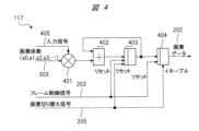
- Fig. 4 is a block diagram showing an example of a pixel integration processing unit according to an embodiment.
- the pixel integration processing unit 117 includes at least a multiplier 401, an adder 402, a flip-flop circuit (hereinafter also referred to as an FF circuit) 403 for holding data during integration processing, and a latch circuit 404 for storing data for which integration processing has been completed and outputting the data to the image memory 119 as pixel data.
- At least an input signal 405 obtained by converting a secondary electron signal detected by the detector 108 (Fig. 1) into a digital signal by the A/D conversion unit 118 (Fig. 1), a pixel coefficient 303 output from the pixel coefficient storage unit 116 (Fig. 3), a frame control signal 203, and a pixel switching signal 205 are input to the pixel integration processing unit 117.
- the multiplier 401 multiplies the input signal 405 by the pixel coefficient 303, and outputs the multiplication result to the adder 402.
- the adder 402 adds the previous multiplication result held in the FF circuit 403 to the current multiplication result, and updates the value stored in the FF circuit 403 with the addition result.
- the frame control signal 203 is input to both the FF circuit 403 and the latch circuit 404, and the FF circuit 403 and the latch circuit 404 are each reset by the rising edge of the frame control signal 203.
- the FF circuit 403 is also reset by the rising edge of the pixel switching signal 205.
- the latch circuit 404 is enabled by the rising edge of the pixel switching signal 205.
- the FF circuit 403 is reset by the rising edge of the frame control signal 203, so that the FF circuit 403 is reset at the start of one frame.
- the FF circuit 403 is also reset by the rising edge of the pixel switching signal 205. In other words, after the pixel switching signal 205 rises, the addition result of the adder 402 is accumulated in the FF circuit 403 during the period until the next rising edge of the signal.
- pixel switching signal 205 rises and then rises two cycles of clock signal CLK.
- input signal 405 and pixel coefficient 303 "a0" are multiplied by multiplier 401, and the multiplication result and the output of reset FF circuit 403 are added by adder 402 and stored in FF circuit 403.
- input signal 405 and pixel coefficient 303 "a0" are multiplied by multiplier 401, and the multiplication result and the multiplication result of the first cycle stored in FF circuit 403 are added by adder 402 and stored in FF circuit 403.
- the latch circuit 404 is also reset by the rising edge of the frame control signal 203, so at the start of one frame, the latch circuit 404 is reset. After that, the rising edge of the pixel switching signal 205 causes the latch circuit 404 to enter an enabled state. In the enabled state, the latch circuit 404 takes in the output of the FF circuit 403 and outputs it as pixel data 202.
- "a0" to "a3" indicate pixel coefficients (first pixel coefficients) set based on the characteristics of the VC method application area.
- the position of the VC method application area in the sample 106 is expressed in X and Y coordinates as (X0, Y0) to (X3, Y0).
- pixel coefficients (second pixel coefficients) set for areas outside the VC method application area are also stored in the LUT and are integrated with the input signal in the pixel integration processing unit 117 shown in Figure 4.
- the scanning speed is set to, for example, one cycle of the clock signal CLK, and the second pixel coefficient is set based on this scanning speed.
- the area outside the VC law application area is, for example, the entire area in one frame except for the VC law application area. This eliminates the need to set the position of the area outside the VC law application area, as shown in Figure 1.
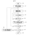
- Fig. 5 is a flow chart showing the operation of the controller according to the embodiment.
- the operation of the pixel coefficient storage unit and pixel accumulation processing unit according to the first embodiment will be described with reference to Figs. 1, 3 to 5.
- the raster trajectory is only an example, and is not limited to this.
- it is assumed that pixel coefficients are supplied to the LUT 302 of the pixel coefficient storage unit 116 from the scanning trajectory generation unit 114, and that pixel coefficients have already been stored in each element of the LUT 302.
- step 500 the controller 109 starts scanning.
- step 501 the controller 109 asserts the frame control signal 203 and initializes the image memory 119.
- the controller 109 also initializes the address (address value indicating the X coordinate and Y coordinate) of the address counter 301 in the pixel coefficient storage unit 116. This initializes the address value that specifies the elements of the image memory 119 and the elements of the LUT 302.
- step 502 the controller 109 uses the address counter 301 to select an element specified by the address value initialized in step 501 from the elements of the LUT 302 in the pixel coefficient storage unit 116, reads (updates) the pixel coefficient 303 stored in the selected element, and in response to the rising edge of the frame control signal 203, initializes the FF circuit 403 in the pixel integration processing unit 117 and initializes the pixel data (pixel value) 202 latched in the latch circuit 404.
- step 503 the controller 109 executes an accumulation process in the pixel accumulation processing unit 117 using the read pixel coefficient 303 and the input signal. That is, the accumulation process is executed using the multiplier 401, adder 402, and FF circuit 403 shown in FIG. 4. Each time this accumulation process is completed, the controller 109 determines in step 504 whether the pixel switching signal 205 is asserted or not. In other words, each time the clock signal CLK shown in FIG. 2 rises, it is determined whether the pixel switching signal 205 is rising or not.
- step 504 If it is determined in step 504 that the pixel switching signal 205 is not asserted (No), the controller 109 repeats the accumulation process in step 503 until the pixel switching signal 205 is asserted, and an accumulated value is obtained.
- multiplication is performed between the same pixel coefficient and the same input signal for the number of cycles of the clock signal CLK from when the pixel switching signal 205 is asserted, to when it is negated and then asserted again, and the result is added to the previous multiplication result to obtain an accumulated value.
- the controller 109 enables the latch circuit 404 in step 505, updates the latch circuit 404, updates the pixel data 202, and stores it in the pixel memory 119. That is, the updated pixel data 202 is stored in the pixel memory 119, and the current address value (X coordinate) is updated.
- the pixel data 202 stored in the pixel memory 119 is pixel data obtained by performing an integration process between the pixel coefficient and the input signal in the pixel integration processing unit 117 for the number of cycles of the clock signal CLK in the interval between the rising edges of the pixel switching signal 205.
- step 506 the controller 109 determines whether or not a line switch has occurred based on the line control signal 204. If the line control signal 204 is not negated, the controller 109 determines that a line switch has not occurred, and returns to step 502 to execute processing. That is, in step 502, the controller 109 initializes the pixel values and updates the pixel coefficients, and in steps 503 and 504, it executes an accumulation process using the updated pixel coefficients and the updated input signal, and in step 505, it stores the pixel data acquired by the accumulation process in the updated address value.
- the address value is updated in step 505 by updating the address generated by the address counter 301 in the pixel coefficient storage unit 116 in response to the rising edge of the pixel switching signal 205. For example, if the current address (X coordinate, Y coordinate) generated by the address counter 301 is the address value (X0, Y0), the address counter 301 updates the address to the address value (X1, Y0) in response to the rising edge of the pixel switching signal 205.
- the control signal (X/Y control signal) output by the control signal generation unit 115 to control the deflector 104 corresponds to the address generated by the address counter 301.
- the address value generated by the address counter 301 when the address value generated by the address counter 301 is updated, the position on the sample 106 where the electron beam 103 is irradiated also changes accordingly, and the A/D conversion unit 118 outputs an input signal according to the secondary electrons from the position where the electron beam 103 is irradiated. Therefore, when the address value generated by the address counter 301 is updated, the input signal input to the multiplier 401 is also updated. That is, the multiplier 401 is supplied with the updated pixel coefficient and an input signal corresponding to the secondary electrons at the position on the sample 106 that corresponds to the updated address value, and multiplication is performed between them.
- step 506 determines in step 506 that the line control signal 204 is negated and a line switch has occurred.
- the controller 109 then executes step 507.
- step 507 the controller 109 determines whether one frame has ended based on the frame control signal 203.
- step 507 if the frame control signal 203 is not negated, the controller 109 determines that one frame has not ended and then executes step 508.
- step 508 the controller 109 initializes and updates the address generated by the address counter 301. That is, in response to the assertion of the line control signal 204, the address counter 301 updates the address value of the Y coordinate and initializes the address value of the X coordinate. That is, the address counter 301 initializes the value of the X coordinate indicating the pixel position and updates the value of the Y coordinate indicating the line position. Specifically, the address counter 301 outputs the address value (e.g., X0, Y1) with the line position and pixel position changed.
- the address counter 301 outputs the address value (e.g., X0, Y1) with the line position and pixel position changed.
- steps 502 to 507 are executed.
- the pixel coefficient specified by the address value (X0, Y1) is read out from the LUT 302, and the input signal input to the multiplier 401 is a signal based on secondary electrons at the position on the sample 106 specified by the X/Y control signal corresponding to the address value (X0, Y1).
- the frame control signal 203 is negated.
- the controller 109 ends the pixel accumulation process in step 509.
- the pixel data 202 for one frame generated by the image accumulation process is stored in the image memory 119 and is output to, for example, a display device as an image captured by scanning.
- FIG. 6 is a plan view showing an example of an image captured by scanning a sample once by the charged particle beam device according to the embodiment.
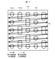
- FIG. 7 is a schematic plan view showing an example of a scanning pattern when the sample is scanned to acquire the captured image of FIG. 6.
- FIGS. 6 and 7 show a case where the user sets the scanning conditions as in the GUI screen 110 shown in FIG. 1. That is, it is assumed that the scanning trajectory is set to a raster trajectory as shown in FIG. 1.
- Figures 6 and 7 show a case in which multiple VC method application areas with multiple different areas and shapes, and areas outside the VC method application area, are set within an area scanned in one go as one frame.
- 120 indicates one frame of an image acquired in one scan
- 602_A and 602_B indicate partial images of the VC method application area of different areas and shapes
- 603 indicates a partial image of a normal surface scan outside the VC method application area.
- the surface of the sample 106 is scanned in a scanning pattern as shown in FIG. 7. That is, in the VC method application areas 702_A and 702_B of the sample 106 corresponding to the partial images 602_A and 602_B, scanning with the electron beam 103 is performed at a first scanning speed, and in the outside of the VC method application area 703 of the sample 106 corresponding to the normal surface scanning partial image 603, scanning with the electron beam 103 is performed at a second scanning speed different from the first scanning speed.
- the second scanning speed is set to a value faster than the first scanning speed.
- the double arrow line RL indicates a return line
- the return line RL is a switching portion of the raster trajectory and is a trajectory that does not affect the acquisition of the image.
- the user when VC method application regions 702_A, 702_B are set on the sample 106, the user can arbitrarily set, for each of the VC method application regions 702_A, 702_B, the position of the region, the scanning speed for each pixel when scanning the region, and the pixel coefficient when scanning the region.
- the user can arbitrarily set the scanning speed for each pixel when scanning the region, and the pixel coefficient when scanning the region.
- FIG. 7 an example is shown in which the same value of the first scanning speed is set for multiple VC method application areas 702_A, 702_B, but this is not limited to this. In other words, if there are multiple VC method application areas (701_A, 701_B) on the sample 106 as in FIG. 7, a different value of the first scanning speed may be set for each VC method application area.
- multiple VC method application areas and non-VC method application areas are set on the same scanning orbit (line).
- the scanning speed of the electron beam changes to a first scanning speed and a second scanning speed on the same scanning orbit.
- partial images 602_A and 602_B of the VC method application area and a normal surface scanning partial image 603 outside the VC method application area can be obtained, and one frame of captured image 120 can be generated.
- the user can arbitrarily set a pixel coefficient for each minute area on the sample that corresponds to one pixel of the captured image, making it possible to obtain an image with good VC contrast while shortening the beam irradiation time on that area. Furthermore, a partial image of the VC method application area and a partial image obtained by performing a normal surface scan outside the VC method application area can be obtained as one frame of an image in a single scan, eliminating steps such as preliminary observation and confirmation of positional validity, improving the convenience of scanning and shortening the observation time.
- the VC method application areas 702_A and 702_B can be regarded as the first surface, and the area 703 outside the VC method application area can be regarded as the second surface.
- scanning is performed at a first scanning speed on the first surface, and scanning is performed at a second scanning speed on the second surface.
- the solid line trajectory portion where scanning is performed at the first scanning speed can be regarded as the first scanning trajectory (first speed trajectory)
- the dashed line trajectory portion where scanning is performed at the second speed can be regarded as the second scanning trajectory (second speed trajectory).
- the user sets an appropriate scanning speed and pixel coefficients (first pixel coefficient, second pixel coefficient) for each of the VC method application area and outside the VC method application area, for example, on the GUI screen 110.
- the scanning speed and pixel coefficients set outside the VC method application area are, for example, scanning speeds and pixel coefficients suitable for normal surface scanning (surface observation), and the pixel coefficients outside the VC method application area are set based on the scanning speed outside the VC method application area.
- first speed trajectory scanning is performed at a scanning speed suitable for the VC method, and an image of a first partial region corresponding to the first surface (partial images 602_A, 602_B) is generated using an input signal based on secondary electrons from the first surface and pixel coefficients suitable for the VC method.
- second speed trajectory scanning is performed at a scanning speed suitable for normal surface scanning, and an image of a second partial region corresponding to the second surface (partial image 603) is generated using an input signal based on secondary electrons from the second surface and pixel coefficients suitable for normal surface scanning.
- REFERENCE SIGNS LIST 100 Charged particle beam device 101 Scanning electron microscope 102 Electron gun 104 Deflector 108 Detector 106 Sample 109 Controller 110 GUI screen 114 Scanning trajectory generation unit 115 Control signal generation unit 116 Pixel coefficient storage unit 117 Pixel integration processing unit 118 A/D conversion unit 119 Pixel memory
Landscapes
- Chemical & Material Sciences (AREA)
- Analytical Chemistry (AREA)
- General Health & Medical Sciences (AREA)
- Life Sciences & Earth Sciences (AREA)
- Health & Medical Sciences (AREA)
- Biochemistry (AREA)
- Physics & Mathematics (AREA)
- General Physics & Mathematics (AREA)
- Immunology (AREA)
- Pathology (AREA)
- Engineering & Computer Science (AREA)
- Computer Vision & Pattern Recognition (AREA)
- Analysing Materials By The Use Of Radiation (AREA)
Abstract
Description
実施の形態では、走査型電子顕微鏡を備えた荷電粒子線装置を用いて、半導体デバイスの観察、特に半導体デバイスをVC観察する場合を例として説明する。荷電粒子線装置を用いて、VC法で観察する場合、VC法を適用する領域(以下、VC法適用領域とも称する)の撮像画像と、VC法を適用しない領域(以下、VC法適用領域外とも称する)の撮像画像との間のコントラスト(輝度レベル)比を高くすることが重要である。なお、VC法適用領域外の撮像画像は、VC法を適用しない領域を、通常の表面走査を行うことで取得した撮像画像に該当する。
図1は、実施の形態に係る荷電粒子線装置の構成を示すブロック図である。図1において、100は、実施の形態1に係る荷電粒子線装置を示している。荷電粒子線装置100は、走査型電子顕微鏡101と走査型電子顕微鏡101を制御するコントローラ109とを備えている。
走査型電子顕微鏡101は、電子銃102と、走査用偏向器(以下、単に偏向器とも称する)104と、試料台105と、検出器108とを備えている。
次に、コントローラ109を説明する。コントローラ109は、ユーザ(図示せず)が設定した走査(スキャン)条件およびパラメータに基づいて、走査型電子顕微鏡101における電子ビームの走査を制御するとともに、走査型電子顕微鏡101からの検出信号に基づいた撮像画像の生成を行う。
図1において、110は、コントローラ109によって、表示装置に表示されているGUI画面を示している。ユーザは、マウスおよびキーボード等の入力装置を操作して、GUI画面110に表示されている項目に対して、選択あるいは数値の入力等を行う。
ユーザは、領域111において、電子ビーム103の走査方法を選択する。すなわち、図1に示した例では、走査方法は、ラスター、フラットおよびスネークの3つの走査方法によって構成されている。ユーザは、領域111において、この3つの走査方法から1つの走査方法を選択する。電子ビーム103は、選択された走査方法によって決まる軌道(走査軌道)に合うように、偏向器による偏向によって、移動する。なお、図1に示されている例では、電子ビーム103の走査方法としては、ラスターが選択されており、走査軌道は、ラスター軌道が選択されている。
ユーザは、領域112において、VC法適用領域の走査に関するパラメータを設定(数値の入力)する。試料106に設定するVC法適用領域の個数は、1つに限定されない。すなわち、試料106に対して、複数のVC法適用領域を設定してもよい。図1に示した領域112には、VC法適用領域の個数を指定する領域であるVC法適用領域数が存在し、数値“2”が設定されている。これにより、2つのVC法適用領域が設定可能となっている。勿論、VC法適用領域数に設定する数値は、“1”でも“3”以上でもよい。
ユーザは、領域113において、VC法適用領域外の領域の走査に関するパラメータを設定する。VC法適用領域外の領域は、通常の表面走査を行う領域に該当し、ユーザは、領域113において、通常の表面走査を行う領域の走査に関するパラメータを設定(数値を入力)する。この通常の表面走査を行う領域のパラメータとしては、例えば、走査速度や画素係数があり、ユーザは、領域113において、これらを設定する。勿論、走査速度と画素係数は、画素毎に変更してもよい。
前記した3つの領域以外に、ユーザが設定する項目としては、例えば、取得する撮像画像の大きさ(画像サイズ)を指定する領域が、GUI画面110には存在する。なお、図1の例では、画像サイズ指定領域に、画像サイズとして、800x600の数値が、ユーザによって直接入力されている。
次に、コントローラ109の構成例を説明する。コントローラ109は、走査軌道生成ユニット114、制御信号生成ユニット115、画素係数格納ユニット116、画素積算処理ユニット117、A/D(アナログ/デジタル)変換ユニット118および画素メモリ119と、を備えている。コントローラ109は、プロセッサを備えており、プロセッサが、図示しない不揮発性メモリに格納されたプログラムを実行することで、走査軌道生成ユニット114、制御信号生成ユニット115、画素係数格納ユニット116および画素積算処理ユニット117等を実現する。プロセッサの一例としては、CPUやGPUが考えられるが、所定の処理を実行する主体であれば他の半導体デバイスでもよい。勿論、これらのユニットは、論理回路、順序回路等を組み合わせて実現してもよい。
次に、前記した画像生成制御信号および画素データ202のタイミングを、図面を用いて説明する。図2は、実施の形態に係る画像生成制御信号と画素データとの関係を示すタイミング図である。図2において、横軸は時間を示し、縦軸は電圧を示している。また、図2に示したクロック信号CLKは、基準となるクロック信号を示している。特に制限されないが、コントローラ109は、このクロック信号CLKに同期して動作する。
図3は、実施の形態に係る画素係数格納ユニットの一例を示すブロック図である。図3に示されているように、画素係数格納ユニット116は、少なくともアドレスカウンタ301とLUT302とを備えている。
図4は、実施の形態に係る画素積算処理ユニットの一例を示すブロック図である。画素積算処理ユニット117は、図4に示すように、少なくとも、乗算器401、加算器402、積算処理中のデータを保持するフリップフロップ回路(以下、FF回路とも称する)403および積算処理が完了したデータを格納し、画素データとして画像メモリ119に出力するためのラッチ回路404を備えている。画素積算処理ユニット117には、少なくとも、検出器108(図1)で検出された二次電子信号をA/D変換ユニット118(図1)でデジタル信号に変換することで取得された入力信号405と、画素係数格納ユニット116(図3)から出力された画素係数303と、フレーム制御信号203と、画素切り替え信号205とが入力される。
図5は、実施の形態に係るコントローラの動作を示すフローチャートである。次に、実施の形態1に係る画素係数格納ユニットおよび画素積算処理ユニットの動作を、図1、図3~図5を用いて説明する。ここでは、ユーザが、走査軌道として、図1に示したようにラスター軌道を設定した場合を例にして説明する。勿論、ラスター軌道は一例であって、これに限定されるものではない。また、画素係数格納ユニット116のLUT302には、走査軌道生成ユニット114から、画素係数が供給され、LUT302の各要素には、既に画素係数が格納されているものとする。
実施の形態に係る荷電粒子線装置100によって撮像された撮像画像の例を、次に説明する。図6は、実施の形態に係る荷電粒子線装置によって、試料を1回スキャンして取得した撮像画像の一例を示す平面図である。また、図7は、図6の撮像画像を取得するために、試料をスキャンしたときの走査パターンの一例を示す模式的な平面図である。図6および図7は、ユーザが、図1に示したGUI画面110のように走査条件を設定した場合が示されている。すなわち、走査軌道は、図1に示せているようにラスター軌道に設定されているものとする。
101 走査型電子顕微鏡
102 電子銃
104 偏向器
108 検出器
106 試料
109 コントローラ
110 GUI画面
114 走査軌道生成ユニット
115 制御信号生成ユニット
116 画素係数格納ユニット
117 画素積算処理ユニット
118 A/D変換ユニット
119 画素メモリ
Claims (10)
- 電子銃と、偏向器と、検出器と、試料が置かれる試料台と、コントローラとを有する装置であって、
撮像画像の作成指示を受信した前記コントローラは:
・ VC法適用領域指定を受信し、
・ 所定走査軌道に基づいて生成される制御信号を前記偏向器に送りつつ、前記検出器から前記試料からの二次電子検出信号を受信し、
・ 前記二次電子検出信号に基づいて前記撮像画像を生成し、
ここで、前記撮像画像は、以下の部分領域を含む:
VC法に適した第1部分領域と、
前記試料の表面観察に適した第2部分領域と、
装置。 - 請求項1記載の装置において、
前記所定走査軌道は:
前記VC法適用領域指定に対応した前記試料上の第1表面を、前記VC法に適した第1走査速度で走査する、第1速度軌道と、
前記VC法適用領域指定に対応しない前記試料上の第2表面を、前記第1走査速度より高速な第2走査速度で走査する、第2速度軌道と、を含み、
前記第1部分領域の画像の前記生成は、第1係数を用いて行われ、
前記第2部分領域の画像の前記生成は、前記第2走査速度に基づいて決められる第2係数を用いて行われ、
前記第1走査速度と前記第1係数は、前記第1表面の特性に基づいて決定された値である、
装置。 - 請求項2に記載の装置において、
前記第1走査速度および前記第2走査速度は、前記電子銃からの電子ビームが前記第1表面および前記第2表面に照射されている時間に相当する、
装置。 - 請求項3に記載の装置において、
前記所定走査軌道は、前記電子ビームによる1スキャンの1ラインを含み、
同一の前記1ラインにおいて、前記第1表面は前記第1走査速度で走査され、前記第2表面は前記第2走査速度で走査される、
装置。 - 請求項4に記載の装置において、
前記第1部分領域の画像は、前記二次電子検出信号に基づいた前記第1表面に係る画素データと前記第1係数との演算によって生成され、
前記第2部分領域の画像は、前記二次電子検出信号に基づいた前記第2表面に係る画素データと前記第2係数との演算によって生成される、
装置。 - 請求項5に記載の装置において、
前記第1部分領域の画像と、前記第2部分領域の画像は、前記電子ビームによる1スキャンによって取得される1フレームに含まれている、
装置。 - 請求項1に記載の装置において、
前記撮像画像の前記作成指示は、GUIにおいて行われる、
装置。 - 電子銃と、偏向器と、検出器と、試料が置かれる試料台と、コントローラとを備える装置の制御方法であって、
前記コントローラは、所定走査軌道に基づいて生成される制御信号を前記偏向器に送りつつ、前記検出器から前記試料からの二次電子検出信号を受信し、前記二次電子検出信号に基づいて撮像画像を生成し、
ここで、前記コントローラは、
前記試料において、VC法適用領域として指定された第1部分領域に係る第1画像を生成し、
前記第1部分領域とは異なる第2部分領域に対して、前記試料の表面観察に適した第2画像を生成する、
制御方法。 - 請求項8記載の制御方法において、
前記コントローラは、
前記VC法適用領域として指定された前記第1部分領域に対応する前記試料上の第1表面を、前記制御信号によって、VC法に適した第1走査速度で走査し、走査により取得された画素データと第1係数とに基づいて、前記第1画像を生成し、
前記第2部分領域に対応する前記試料上の第2表面を、前記制御信号によって、前記第1走査速度より高速な第2走査速度で走査し、走査により取得された画素データと第2係数とに基づいて、前記第2画像を生成し、
ここで、前記第1走査速度と前記第1係数は、前記第1表面の特性に基づいて決定された値である、
制御方法。 - 請求項8または9に記載の制御方法を、前記コントローラに実行させるプログラム。
Priority Applications (4)
| Application Number | Priority Date | Filing Date | Title |
|---|---|---|---|
| PCT/JP2023/023295 WO2024262000A1 (ja) | 2023-06-23 | 2023-06-23 | 装置およびその制御方法ならびにプログラム |
| KR1020257028398A KR20250139863A (ko) | 2023-06-23 | 2023-06-23 | 장치 및 그 제어 방법 그리고 프로그램 |
| JP2025527377A JPWO2024262000A1 (ja) | 2023-06-23 | 2023-06-23 | |
| TW113115310A TWI910613B (zh) | 2023-06-23 | 2024-04-24 | 電子束裝置及其控制方法以及電子束裝置的控制程式 |
Applications Claiming Priority (1)
| Application Number | Priority Date | Filing Date | Title |
|---|---|---|---|
| PCT/JP2023/023295 WO2024262000A1 (ja) | 2023-06-23 | 2023-06-23 | 装置およびその制御方法ならびにプログラム |
Publications (1)
| Publication Number | Publication Date |
|---|---|
| WO2024262000A1 true WO2024262000A1 (ja) | 2024-12-26 |
Family
ID=93935024
Family Applications (1)
| Application Number | Title | Priority Date | Filing Date |
|---|---|---|---|
| PCT/JP2023/023295 Ceased WO2024262000A1 (ja) | 2023-06-23 | 2023-06-23 | 装置およびその制御方法ならびにプログラム |
Country Status (4)
| Country | Link |
|---|---|
| JP (1) | JPWO2024262000A1 (ja) |
| KR (1) | KR20250139863A (ja) |
| TW (1) | TWI910613B (ja) |
| WO (1) | WO2024262000A1 (ja) |
Citations (4)
| Publication number | Priority date | Publication date | Assignee | Title |
|---|---|---|---|---|
| JP2007095822A (ja) * | 2005-09-27 | 2007-04-12 | Fujitsu Ltd | 半導体装置のコンタクト不良検査方法及びその検査方法が適用される半導体装置 |
| JP2008177282A (ja) * | 2007-01-17 | 2008-07-31 | Renesas Technology Corp | 半導体装置の製造方法 |
| JP2009092673A (ja) * | 2008-12-26 | 2009-04-30 | Hitachi Ltd | レビューsem |
| WO2011102511A1 (ja) * | 2010-02-22 | 2011-08-25 | 株式会社日立ハイテクノロジーズ | 回路パターン検査装置 |
Family Cites Families (3)
| Publication number | Priority date | Publication date | Assignee | Title |
|---|---|---|---|---|
| TWI458967B (zh) * | 2005-02-17 | 2014-11-01 | 荏原製作所股份有限公司 | 電子射線裝置 |
| JP6334243B2 (ja) | 2014-04-25 | 2018-05-30 | 株式会社日立ハイテクノロジーズ | 荷電粒子線装置 |
| WO2016143450A1 (ja) * | 2015-03-10 | 2016-09-15 | 株式会社荏原製作所 | 検査装置 |
-
2023
- 2023-06-23 WO PCT/JP2023/023295 patent/WO2024262000A1/ja not_active Ceased
- 2023-06-23 KR KR1020257028398A patent/KR20250139863A/ko active Pending
- 2023-06-23 JP JP2025527377A patent/JPWO2024262000A1/ja active Pending
-
2024
- 2024-04-24 TW TW113115310A patent/TWI910613B/zh active
Patent Citations (4)
| Publication number | Priority date | Publication date | Assignee | Title |
|---|---|---|---|---|
| JP2007095822A (ja) * | 2005-09-27 | 2007-04-12 | Fujitsu Ltd | 半導体装置のコンタクト不良検査方法及びその検査方法が適用される半導体装置 |
| JP2008177282A (ja) * | 2007-01-17 | 2008-07-31 | Renesas Technology Corp | 半導体装置の製造方法 |
| JP2009092673A (ja) * | 2008-12-26 | 2009-04-30 | Hitachi Ltd | レビューsem |
| WO2011102511A1 (ja) * | 2010-02-22 | 2011-08-25 | 株式会社日立ハイテクノロジーズ | 回路パターン検査装置 |
Also Published As
| Publication number | Publication date |
|---|---|
| JPWO2024262000A1 (ja) | 2024-12-26 |
| TW202500986A (zh) | 2025-01-01 |
| KR20250139863A (ko) | 2025-09-23 |
| TWI910613B (zh) | 2026-01-01 |
Similar Documents
| Publication | Publication Date | Title |
|---|---|---|
| KR102267218B1 (ko) | 계측 장치 및 관측 조건의 설정 방법 | |
| US8658987B2 (en) | Circuit-pattern inspection device | |
| JP4512471B2 (ja) | 走査型電子顕微鏡及び半導体検査システム | |
| JP2011228741A (ja) | 半導体ウェーハ検査装置 | |
| US20090026369A1 (en) | Electron Beam Inspection System and an Image Generation Method for an Electron Beam Inspection System | |
| JP5222994B2 (ja) | 試料観察方法および走査電子顕微鏡 | |
| JP5055015B2 (ja) | 荷電粒子線装置 | |
| TWI910613B (zh) | 電子束裝置及其控制方法以及電子束裝置的控制程式 | |
| US7288763B2 (en) | Method of measurement accuracy improvement by control of pattern shrinkage | |
| JP2011003480A (ja) | Sem式外観検査装置およびその画像信号処理方法 | |
| JP4857240B2 (ja) | 半導体ウェーハ検査装置 | |
| JP4746659B2 (ja) | 回路パターンの検査方法 | |
| JP2004271269A (ja) | パターン検査方法及びパターン検査装置 | |
| JP4719699B2 (ja) | 走査型電子顕微鏡 | |
| JP7290747B2 (ja) | 走査電子顕微鏡 | |
| JP2017199453A (ja) | 荷電粒子線装置 | |
| JP6334243B2 (ja) | 荷電粒子線装置 | |
| JP2005175333A (ja) | 回路パターン検査方法とその装置 | |
| US7952072B2 (en) | Test apparatus | |
| JP4695959B2 (ja) | 集束イオンビーム装置及び集束イオンビーム装置の加工位置設定方法 | |
| JP7392155B2 (ja) | 荷電粒子線装置、およびスキャン波形生成方法 | |
| JP3790629B2 (ja) | 走査型荷電粒子ビーム装置及び走査型荷電粒子ビーム装置の動作方法 | |
| JP2986995B2 (ja) | 二次電子像変形補正装置 | |
| JPH0329867A (ja) | 電子ビーム装置による電圧分布像の観測法 | |
| JP2012054174A (ja) | 走査電子顕微鏡装置及びそれを用いた画像取得方法 |
Legal Events
| Date | Code | Title | Description |
|---|---|---|---|
| 121 | Ep: the epo has been informed by wipo that ep was designated in this application |
Ref document number: 23942432 Country of ref document: EP Kind code of ref document: A1 |
|
| ENP | Entry into the national phase |
Ref document number: 2025527377 Country of ref document: JP Kind code of ref document: A |
|
| WWE | Wipo information: entry into national phase |
Ref document number: 2025527377 Country of ref document: JP |
|
| ENP | Entry into the national phase |
Ref document number: 1020257028398 Country of ref document: KR Free format text: ST27 STATUS EVENT CODE: A-0-1-A10-A15-NAP-PA0105 (AS PROVIDED BY THE NATIONAL OFFICE) |
|
| NENP | Non-entry into the national phase |
Ref country code: DE |
|
| 122 | Ep: pct application non-entry in european phase |
Ref document number: 23942432 Country of ref document: EP Kind code of ref document: A1 |