WO2024257543A1 - 半導体装置 - Google Patents
半導体装置 Download PDFInfo
- Publication number
- WO2024257543A1 WO2024257543A1 PCT/JP2024/018091 JP2024018091W WO2024257543A1 WO 2024257543 A1 WO2024257543 A1 WO 2024257543A1 JP 2024018091 W JP2024018091 W JP 2024018091W WO 2024257543 A1 WO2024257543 A1 WO 2024257543A1
- Authority
- WO
- WIPO (PCT)
- Prior art keywords
- partition
- boundary
- semiconductor device
- resin
- extension
- Prior art date
- Legal status (The legal status is an assumption and is not a legal conclusion. Google has not performed a legal analysis and makes no representation as to the accuracy of the status listed.)
- Ceased
Links
Images







Classifications
-
- H—ELECTRICITY
- H10—SEMICONDUCTOR DEVICES; ELECTRIC SOLID-STATE DEVICES NOT OTHERWISE PROVIDED FOR
- H10W—GENERIC PACKAGES, INTERCONNECTIONS, CONNECTORS OR OTHER CONSTRUCTIONAL DETAILS OF DEVICES COVERED BY CLASS H10
- H10W90/00—Package configurations
- H10W90/811—Multiple chips on leadframes
-
- H—ELECTRICITY
- H10—SEMICONDUCTOR DEVICES; ELECTRIC SOLID-STATE DEVICES NOT OTHERWISE PROVIDED FOR
- H10W—GENERIC PACKAGES, INTERCONNECTIONS, CONNECTORS OR OTHER CONSTRUCTIONAL DETAILS OF DEVICES COVERED BY CLASS H10
- H10W70/00—Package substrates; Interposers; Redistribution layers [RDL]
- H10W70/40—Leadframes
-
- H—ELECTRICITY
- H10—SEMICONDUCTOR DEVICES; ELECTRIC SOLID-STATE DEVICES NOT OTHERWISE PROVIDED FOR
- H10W—GENERIC PACKAGES, INTERCONNECTIONS, CONNECTORS OR OTHER CONSTRUCTIONAL DETAILS OF DEVICES COVERED BY CLASS H10
- H10W70/00—Package substrates; Interposers; Redistribution layers [RDL]
- H10W70/40—Leadframes
- H10W70/411—Chip-supporting parts, e.g. die pads
-
- H—ELECTRICITY
- H10—SEMICONDUCTOR DEVICES; ELECTRIC SOLID-STATE DEVICES NOT OTHERWISE PROVIDED FOR
- H10W—GENERIC PACKAGES, INTERCONNECTIONS, CONNECTORS OR OTHER CONSTRUCTIONAL DETAILS OF DEVICES COVERED BY CLASS H10
- H10W70/00—Package substrates; Interposers; Redistribution layers [RDL]
- H10W70/40—Leadframes
- H10W70/421—Shapes or dispositions
- H10W70/424—Cross-sectional shapes
- H10W70/427—Bent parts
- H10W70/429—Bent parts being the outer leads
-
- H—ELECTRICITY
- H10—SEMICONDUCTOR DEVICES; ELECTRIC SOLID-STATE DEVICES NOT OTHERWISE PROVIDED FOR
- H10W—GENERIC PACKAGES, INTERCONNECTIONS, CONNECTORS OR OTHER CONSTRUCTIONAL DETAILS OF DEVICES COVERED BY CLASS H10
- H10W90/00—Package configurations
-
- H—ELECTRICITY
- H10—SEMICONDUCTOR DEVICES; ELECTRIC SOLID-STATE DEVICES NOT OTHERWISE PROVIDED FOR
- H10W—GENERIC PACKAGES, INTERCONNECTIONS, CONNECTORS OR OTHER CONSTRUCTIONAL DETAILS OF DEVICES COVERED BY CLASS H10
- H10W74/00—Encapsulations, e.g. protective coatings
- H10W74/10—Encapsulations, e.g. protective coatings characterised by their shape or disposition
- H10W74/111—Encapsulations, e.g. protective coatings characterised by their shape or disposition the semiconductor body being completely enclosed
- H10W74/114—Encapsulations, e.g. protective coatings characterised by their shape or disposition the semiconductor body being completely enclosed by a substrate and the encapsulations
-
- H—ELECTRICITY
- H10—SEMICONDUCTOR DEVICES; ELECTRIC SOLID-STATE DEVICES NOT OTHERWISE PROVIDED FOR
- H10W—GENERIC PACKAGES, INTERCONNECTIONS, CONNECTORS OR OTHER CONSTRUCTIONAL DETAILS OF DEVICES COVERED BY CLASS H10
- H10W90/00—Package configurations
- H10W90/701—Package configurations characterised by the relative positions of pads or connectors relative to package parts
- H10W90/751—Package configurations characterised by the relative positions of pads or connectors relative to package parts of bond wires
- H10W90/753—Package configurations characterised by the relative positions of pads or connectors relative to package parts of bond wires between laterally-adjacent chips
-
- H—ELECTRICITY
- H10—SEMICONDUCTOR DEVICES; ELECTRIC SOLID-STATE DEVICES NOT OTHERWISE PROVIDED FOR
- H10W—GENERIC PACKAGES, INTERCONNECTIONS, CONNECTORS OR OTHER CONSTRUCTIONAL DETAILS OF DEVICES COVERED BY CLASS H10
- H10W90/00—Package configurations
- H10W90/701—Package configurations characterised by the relative positions of pads or connectors relative to package parts
- H10W90/751—Package configurations characterised by the relative positions of pads or connectors relative to package parts of bond wires
- H10W90/756—Package configurations characterised by the relative positions of pads or connectors relative to package parts of bond wires between a chip and a stacked lead frame, conducting package substrate or heat sink
Definitions
- This disclosure relates to a semiconductor device.
- the semiconductor device described in this document includes a conductive support member, a semiconductor element, and a sealing resin.
- the conductive support member has a die pad and multiple outer leads.
- the semiconductor element is mounted on the die pad.
- the multiple outer leads are exposed from the sealing resin and are conductive to the semiconductor element.
- the dam bar of the lead frame is cut to separate it into multiple outer leads, and the outer leads are bent by bending.
- the width of the cut portion of the dam bar in the outer lead is larger than the width of the other portions.
- the cut portion of the dam bar in the outer lead may have an unstable shape after processing, such as becoming sharp due to the bending process.
- One of the objectives of this disclosure is to provide a semiconductor device that is an improvement over conventional semiconductor devices.
- one of the objectives of this disclosure is to provide a semiconductor device that is suitable for improving the stability of the shape of the outer lead after bending.
- a semiconductor device provided by one aspect of the present disclosure includes one or more semiconductor elements, a conductive support member, and a sealing resin having a first resin side surface facing one side in a first direction perpendicular to the thickness direction and covering the one or more semiconductor elements.
- the conductive support member includes one or more first outer leads each having a first root portion extending from the first resin side surface in the first direction, a first mounting portion located on one side of the first root portion in the thickness direction, and a first extension portion connected to the first root portion via a first bend portion and connected to the first mounting portion via a second bend portion.
- the first outer lead includes a first partition portion including the first extension portion, a second partition portion including the first root portion and connected to the first partition portion, and a third partition portion including the first mounting portion and connected to the first partition portion.
- the dimension of the first partition portion in the thickness direction and the second direction perpendicular to the first direction is larger than the dimension of the second partition portion in the second direction and the dimension of the third partition portion in the second direction.
- At least one of a first partition boundary, which is the boundary between the first partition and the second partition, and a second partition boundary, which is the boundary between the first partition and the third partition, is located in the first extension portion.
- the above configuration makes it possible to improve the stability of the shape of the outer lead after bending.
- FIG. 1 is a plan view showing a semiconductor device according to a first embodiment of the present disclosure.
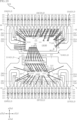
- FIG. 2 is a plan view corresponding to FIG. 1 and seen through the sealing resin.
- FIG. 3 is a front view showing the semiconductor device according to the first embodiment of the present disclosure.
- FIG. 4 is a left side view showing the semiconductor device according to the first embodiment of the present disclosure.
- FIG. 5 is a rear view showing the semiconductor device according to the first embodiment of the present disclosure.
- FIG. 6 is a right side view showing the semiconductor device according to the first embodiment of the present disclosure.
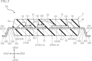
- FIG. 7 is a cross-sectional view taken along line VII-VII in FIG.
- FIG. 8 is a cross-sectional view taken along line VIII-VIII in FIG.
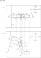
- FIG. 9 is an enlarged view of a main part showing the semiconductor device according to the first embodiment of the present disclosure, in which the upper part is an enlarged view of a part of FIG. 1 and the lower part is an enlarged view of a part of FIG.
- FIG. 10 is an enlarged view of a main part showing the semiconductor device according to the first embodiment of the present disclosure, in which the upper part is an enlarged view of a part of FIG. 1 and the lower part is an enlarged view of a part of FIG.
- FIG. 11 is a plan view showing a process in the manufacture of the semiconductor device according to the first embodiment of the present disclosure.
- FIG. 12 is a plan view showing a semiconductor device according to a first modification of the first embodiment.
- FIG. 13 is a plan view showing a semiconductor device according to a first modification of the first embodiment, seen through a sealing resin.
- FIG. 14 is a front view showing a semiconductor device according to a first modification of the first embodiment.
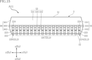
- FIG. 15 is a left side view showing a semiconductor device according to a first modification of the first embodiment.
- FIG. 16 is a rear view showing the semiconductor device according to the first modification of the first embodiment.
- FIG. 17 is a right side view showing a semiconductor device according to a first modification of the first embodiment.
- an object A is formed on an object B" and “an object A is formed on an object B” include “an object A is formed directly on an object B” and “an object A is formed on an object B with another object interposed between the object A and the object B” unless otherwise specified.
- an object A is disposed on an object B” and “an object A is disposed on an object B” include “an object A is disposed directly on an object B” and “an object A is disposed on an object B with another object interposed between the object A and the object B" unless otherwise specified.
- an object A is located on an object B includes “an object A is located on an object B in contact with an object B” and “an object A is located on an object B with another object interposed between the object A and the object B” unless otherwise specified.
- an object A overlaps an object B when viewed in a certain direction includes “an object A overlaps the entire object B” and “an object A overlaps a part of an object B.”
- a surface A faces in direction B is not limited to the case where the angle of surface A with respect to direction B is 90 degrees, but also includes the case where surface A is tilted with respect to direction B.
- a semiconductor device A1 according to a first embodiment of the present disclosure will be described with reference to FIGS. 1 to 10.
- the semiconductor device A1 of this embodiment includes two semiconductor elements 10, an insulating element 12, a conductive support member 2, a plurality of wires 31 to 34, and a sealing resin 5.
- the conductive support member 2 includes a die pad portion 21, a plurality of first outer leads 22, a plurality of second outer leads 23, a plurality of first inner leads 24, and a plurality of second inner leads 25.
- the specific use of the semiconductor device A1 is not limited in any way, but it is, for example, surface-mounted on a wiring board of an inverter device of an electric vehicle or a hybrid vehicle.
- the package format of the semiconductor device A1 is a SOP (Small Outline Package). However, the package format of the semiconductor device A1 is not limited to the SOP.
- FIGS. 1 and 2 are plan views showing the semiconductor device A1.
- FIG. 3 is a front view showing the semiconductor device A1.
- FIG. 4 is a left side view showing the semiconductor device A1.
- FIG. 5 is a rear view showing the semiconductor device A1.
- FIG. 6 is a right side view showing the semiconductor device A1.
- FIG. 7 is a cross-sectional view taken along line VII-VII in FIG. 2.
- FIG. 8 is a cross-sectional view taken along line VIII-VIII in FIG. 2.
- FIG. 9 and FIG. 10 the upper part is an enlarged view of a portion of FIG. 1, and the lower part is an enlarged view of a portion of FIG. 3.
- FIG. 2 is shown through the sealing resin 5 for ease of understanding.
- the through sealing resin 5 is shown by an imaginary line (two-dot chain line).
- the thickness direction (direction in plan view) of the die pad portion 21 (conductive support member 2) is referred to as the "thickness direction z".
- the direction perpendicular to the thickness direction z (the up-down direction in FIG. 1) is referred to as the "first direction x”.
- the direction perpendicular to the thickness direction z and the first direction x (the left-right direction in FIG. 1) is referred to as the "second direction y".
- the semiconductor device A1 is approximately rectangular when viewed in the thickness direction z.
- FIG. 2 is an example of the "one side of the first direction" of the present disclosure and is referred to as the "x1 side of the first direction x", and the upper side in the figures is an example of the "other side of the first direction” of the present disclosure and is referred to as the "x2 side of the first direction x".
- the right side in the figures is referred to as the "y1 side of the second direction y”
- the left side in the figures is referred to as the "y2 side of the second direction y”.
- the lower side in the figure is an example of “one side in the thickness direction” in this disclosure, and is called the “z1 side in the thickness direction z," and the upper side in the figure is called the “z2 side in the thickness direction z.”
- the z2 side in the thickness direction z may be referred to as the upper side
- the z1 side in the thickness direction z may be referred to as the lower side.
- the terms "upper,” “lower,” “upper,” “lower,” “top surface,” and “bottom surface” indicate the relative positional relationship of each component in the thickness direction z, and are not necessarily terms that define the relationship with the direction of gravity.
- the two semiconductor elements 10 and the insulating element 12 are the functional core elements of the semiconductor device A1.
- the two semiconductor elements 10 include a first semiconductor element 11 and a second semiconductor element 13.
- the first semiconductor element 11, the second semiconductor element 13, and the insulating element 12 are each composed of individual elements.
- the first semiconductor element 11, the second semiconductor element 13, and the insulating element 12 are each rectangular with the longer side extending in the second direction y.
- the first semiconductor element 11 is a controller (control element) of a gate driver that drives switching elements such as IGBTs and MOSFETs.
- the first semiconductor element 11 has a circuit that converts a control signal input from an ECU or the like into a PWM control signal, a transmission circuit for transmitting the PWM control signal to the second semiconductor element 13, and a receiving circuit for receiving an electrical signal from the second semiconductor element 13.
- the second semiconductor element 13 is a gate driver (drive element) for driving the switching element.
- the second semiconductor element 13 has a receiving circuit for receiving a PWM control signal, a circuit for driving the switching element based on the PWM control signal, and a transmitting circuit for transmitting an electrical signal to the first semiconductor element 11.
- An example of the electrical signal is an output signal from a temperature sensor arranged near the motor.
- the insulating element 12 is an element for transmitting a PWM control signal or other electric signals in an insulated state.
- the insulating element 12 is an inductive type.
- An insulating transformer is an example of an inductive type insulating element 12.
- An insulating transformer transmits an electric signal in an insulated state by inductively coupling two inductors (coils).
- the insulating element 12 has a substrate made of silicon.
- An inductor made of copper is formed on the substrate.
- the inductors include a transmitting inductor and a receiving inductor, and these inductors are stacked in the thickness direction z.
- a dielectric layer made of silicon dioxide (SiO 2 ) or the like is interposed between the transmitting inductor and the receiving inductor.
- the transmitting inductor and the receiving inductor are electrically insulated by the dielectric layer.
- the insulating element 12 may be a capacitive type.
- a capacitor is an example of a capacitive type insulating element 12.
- the insulating element 12 may be a photocoupler.
- the second semiconductor element 13 requires a power supply voltage higher than that required for the first semiconductor element 11. For this reason, a significant potential difference occurs between the first semiconductor element 11 and the second semiconductor element 13. Therefore, in the semiconductor device A1, the first circuit including the first semiconductor element 11 as a component and the second circuit including the second semiconductor element 13 as a component are insulated from each other by the insulating element 12. The first circuit and the second circuit have relatively different potentials. In the semiconductor device A1, the second circuit has a higher potential than the first circuit. In addition, the insulating element 12 relays mutual signals in the first circuit and the second circuit. For example, in an inverter device for an electric vehicle or a hybrid vehicle, the voltage applied to the ground of the first semiconductor element 11 is about 0V, while the voltage applied to the ground of the second semiconductor element 13 may transiently become 600V or more.
- a plurality of electrodes 111 are provided on the upper surface of the first semiconductor element 11 (the surface facing in the same direction as the mounting surface 211 of the die pad portion 21 described below). The plurality of electrodes 111 are electrically connected to a circuit configured in the first semiconductor element 11.
- a plurality of electrodes 131 are provided on the upper surface of the second semiconductor element 13 (the surface facing in the same direction as the mounting surface 211 described above). The plurality of electrodes 131 are electrically connected to a circuit configured in the second semiconductor element 13.
- the insulating element 12 is located between the first semiconductor element 11 and the second semiconductor element 13 in the second direction y.
- a plurality of first electrodes 121 and a plurality of second electrodes 122 are provided on the upper surface of the insulating element 12 (the surface facing the same direction as the mounting surface 211 described above).
- Each of the plurality of first electrodes 121 and the plurality of second electrodes 122 is conductive to either the transmitting inductor or the receiving inductor.
- the plurality of first electrodes 121 are arranged along the first direction x, and are located closer to the first semiconductor element 11 than the second semiconductor element 13 in the second direction y.
- the plurality of second electrodes 122 are arranged along the first direction x, and are located closer to the second semiconductor element 13 than the first semiconductor element 11 in the second direction y.
- the conductive support member 2 is a member that constitutes a conductive path between the first semiconductor element 11, the second semiconductor element 13, and the insulating element 12 and the wiring board of the inverter device in the semiconductor device A1.
- the conductive support member 2 is made of an alloy containing copper (Cu) in its composition, for example.
- the conductive support member 2 is formed from a lead frame 81 described later.
- the conductive support member 2 carries the first semiconductor element 11, the insulating element 12, and the second semiconductor element 13.
- the conductive support member 2 includes a die pad portion 21, a plurality of first outer leads 22, a plurality of second outer leads 23, a plurality of first inner leads 24, and a plurality of second inner leads 25.
- a plating layer made of silver (Ag), nickel (Ni), gold (Au), etc. may be provided at appropriate locations of the conductive support member 2 as necessary.
- the first semiconductor element 11, the second semiconductor element 13, and the insulating element 12 are mounted on the die pad portion 21.
- the die pad portion 21 has a first die pad 21A and a second die pad 21B.
- the first die pad 21A is arranged on the x1 side of the first direction x.
- the second die pad 21B is arranged on the x2 side of the first direction x.
- the first die pad 21A and the second die pad 21B are spaced apart from each other in the first direction x.
- the semiconductor device A1 the first semiconductor element 11 and the insulating element 12 are mounted on the first die pad 21A, and the second semiconductor element 13 is mounted on the second die pad 21B.
- the die pad portion 21 (first die pad 21A and second die pad 21B) is covered with sealing resin 5.
- the die pad portion 21 (each of the first die pad 21A and second die pad 21B) has a mounting surface 211 facing the z2 side in the thickness direction z.
- the first semiconductor element 11 and the insulating element 12 are mounted on the mounting surface 211 of the first die pad 21A.
- the second semiconductor element 13 is mounted on the mounting surface 211 of the second die pad 21B.
- Each of the first semiconductor element 11, the second semiconductor element 13, and the insulating element 12 is bonded to either the mounting surface 211 of the first die pad 21A or the mounting surface 211 of the second die pad 21B via a conductive bonding material (solder, metal paste, etc.) not shown.
- the thickness of the first die pad 21A and the second die pad 21B (die pad portion 21) is, for example, 100 ⁇ m or more and 300 ⁇ m or less.
- a plurality of through holes 212 are formed in the first die pad 21A.
- Each of the plurality of through holes 212 penetrates the first die pad 21A in the thickness direction z and extends along the second direction y.
- at least one of the plurality of through holes 212 is located between the first semiconductor element 11 and the insulating element 12.
- the plurality of through holes 212 are arranged along the second direction y.
- the first outer leads 22 are members that are joined to a wiring board such as an inverter device to form a conductive path between the semiconductor device A1 and the wiring board. At least one of the first outer leads 22 is electrically connected to the first semiconductor element 11. As shown in FIGS. 1, 2 and 4, the first outer leads 22 are arranged at intervals from each other in the second direction y. The first outer leads 22 are exposed so as to extend from the sealing resin 5 (the first resin side surface 53 described later) to the x1 side of the first direction x. As shown in FIGS. 1, 3 and 5, the first outer leads 22 overlap each other when viewed in the second direction y.
- the first outer leads 22 include a first outer lead 22A at one end, a first outer lead 22B at the other end and a plurality of intermediate first outer leads 22C.
- the first outer lead 22A at one end is located at the end of the first outer leads 22 on the y1 side in the second direction y.
- the other end side first outer lead 22B is located at the end on the y2 side of the multiple first outer leads 22 in the second direction y.
- the multiple intermediate first outer leads 22C are arranged between the one end side first outer lead 22A and the other end side first outer lead 22B.
- Each of the multiple first outer leads 22 (one end side first outer lead 22A, the other end side first outer lead 22B, and multiple intermediate first outer leads 22C) has a first root portion 221, a first mounting portion 222, a first extending portion 223, a first bent portion 224, and a second bent portion 225.
- the first root portion 221 is the root portion of the first outer lead 22. As shown in Figures 1 and 2, the first root portion 221 is located at the end of the first outer lead 22 that is closer to the sealing resin 5 in the first direction x. Therefore, the first root portion 221, the first mounting portion 222 and the first extending portion 223 are also located closer to the sealing resin 5 in the first direction x. The first root portion 221 is located higher in the thickness direction z (on the z2 side in the thickness direction z) than the first mounting portion 222, and protrudes from the center of the sealing resin 5 in the thickness direction z.
- the first mounting portion 222 is the tip portion of the first outer lead 22.
- the first mounting portion 222 is a portion that is joined to the circuit board when the semiconductor device A1 is mounted on the circuit board. As shown in FIG. 1 and FIG. 2, the first mounting portion 222 is located at the end opposite the sealing resin 5 in the first direction x. Therefore, the first mounting portion 222 is located farther from the sealing resin 5 in the first direction x than the first root portion 221 and the first extension portion 223.
- the first mounting portion 222 is located lower in the thickness direction z than the first root portion 221 (on the z1 side in the thickness direction z).
- the first extension portion 223 is connected to the first root portion 221 via the first bend portion 224 and to the first mounting portion 222 via the second bend portion 225.
- the first extension portion 223 is inclined with respect to the first root portion 221 and the first mounting portion 222 when viewed in the second direction y. Furthermore, the first extension portion 223 is inclined with respect to the thickness direction z when viewed in the second direction y.
- the first bent portion 224 is interposed between the first root portion 221 and the first extension portion 223.
- the first bent portion 224 bends downward in the thickness direction z from the first root portion 221.
- the second bent portion 225 is interposed between the first mounting portion 222 and the first extension portion 223.
- the second bent portion 225 bends upward in the thickness direction z from the first mounting portion 222.
- the first bent portion 224 and the second bent portion 225 are each curved when viewed in the second direction y.
- the first outer lead 22 includes a first partition 226, a second partition 227, and a third partition 228.
- the first partition 226 includes a first extension 223.
- the second partition 227 includes a first root 221 and is connected to the first partition 226.
- the third partition 228 includes a first mounting portion 222 and is connected to the first partition 226.
- the dimension w1 in the second direction y of the first partition 226 is greater than the dimension w2 in the second direction y of the second partition 227 and the dimension w3 in the second direction y of the third partition 228.
- the first partition 226 corresponds to a portion of a dam bar 816 of the lead frame 81 described later, and is a portion that is wider than other portions by cutting the dam bar 816. In FIG. 9, the first partition 226 is hatched.
- the first partition boundary 226a which is the boundary between the first partition 226 and the second partition 227, is located at the first root 221.
- the second partition boundary 226b which is the boundary between the first partition 226 and the third partition 228, is located at the first extension 223.
- the distance (first distance d1) between the first boundary 2201, which is the boundary between the first bend 224 and the first extension 223, and the second partition boundary 226b is, for example, 0.01 mm or more and 1.0 mm or less, and preferably 0.01 mm or more and 0.05 mm or less.
- first distance d1 between the first boundary 2201 and the second partition boundary 226b is 1/20 times or more and 1/2 times or less, and preferably 1/10 times or more and 1/4 times or less, of the dimension t1 in the thickness direction z of the first root 221.
- the multiple first inner leads 24 are covered with sealing resin 5.
- the first inner leads 24 extend inwardly from each of the multiple first outer leads 22 into the sealing resin 5.
- the multiple first inner leads 24 include a first inner lead 24A on one end side, a first inner lead 24B on the other end side, and multiple intermediate first inner leads 24C.
- the first inner lead 24A on one end side is connected to the end on the x2 side of the first outer lead 22A on the first direction x.
- the end of the first inner lead 24A on the opposite side to the first outer lead 22A on the one end side is connected to the first die pad 21A.
- the first inner lead 24B on the other end side is connected to the end on the x2 side of the first direction x of the first outer lead 22B on the other end side.
- the end of the first inner lead 24B on the opposite side to the first outer lead 22B on the other end side is connected to the first die pad 21A.
- Each of the multiple intermediate first inner leads 24C is connected to the end on the x2 side of the first direction x of one of the multiple intermediate first outer leads 22C, and extends close to the first die pad 21A.
- the second outer leads 23 are members that are joined to a wiring board such as an inverter device to form a conductive path between the semiconductor device A1 and the wiring board. At least one of the second outer leads 23 is conductive to the second semiconductor element 13. As shown in Figures 1, 2 and 6, the second outer leads 23 are arranged at intervals from each other in the second direction y. The second outer leads 23 are exposed so as to extend from the sealing resin 5 (the second resin side surface 54 described later) to the x2 side of the first direction x. As shown in Figures 1, 3 and 5, the second outer leads 23 overlap each other when viewed in the second direction y.
- the second outer leads 23 include a one-end side second outer lead 23A, an other-end side second outer lead 23B and a plurality of intermediate second outer leads 23C.
- the one-end side second outer lead 23A is located at the end of the second outer leads 23 on the y1 side in the second direction y.
- the other end side second outer lead 23B is located at the end on the y2 side of the multiple second outer leads 23 in the second direction y.
- the multiple intermediate second outer leads 23C are arranged between the one end side second outer lead 23A and the other end side second outer lead 23B.
- Each of the multiple second outer leads 23 (one end side second outer lead 23A, the other end side second outer lead 23B, and multiple intermediate second outer leads 23C) has a second root portion 231, a second mounting portion 232, a second extending portion 233, a third bent portion 234, and a fourth bent portion 235.
- the second root portion 231 is the root portion of the second outer lead 23. As shown in Figures 1 and 2, the second root portion 231 is located at the end of the second outer lead 23 that is closer to the sealing resin 5 in the first direction x. Therefore, the second root portion 231, the second mounting portion 232 and the second extension portion 233 are also located closer to the sealing resin 5 in the first direction x. The second root portion 231 is located higher in the thickness direction z (on the z2 side in the thickness direction z) than the second mounting portion 232, and protrudes from the center of the sealing resin 5 in the thickness direction z.
- the second mounting portion 232 is the tip portion of the second outer lead 23.
- the second mounting portion 232 is a portion that is joined to the circuit board when the semiconductor device A1 is mounted on the circuit board. As shown in Figures 1 and 2, the second mounting portion 232 is located at the end opposite the sealing resin 5 in the first direction x. Therefore, the second mounting portion 232 is located farther from the sealing resin 5 in the first direction x than the second root portion 231 and the second extension portion 233.
- the second mounting portion 232 is located lower in the thickness direction z than the second root portion 231 (on the z1 side in the thickness direction z).
- the second extension portion 233 is connected to the second root portion 231 via the third bend portion 234 and to the second mounting portion 232 via the fourth bend portion 235.
- the second extension portion 233 is inclined with respect to the second root portion 231 and the second root portion 232 when viewed in the second direction y. Furthermore, the second extension portion 233 is inclined with respect to the thickness direction z when viewed in the second direction y.
- the third bend 234 is interposed between the second root portion 231 and the second extension portion 233.
- the third bend 234 bends downward in the thickness direction z from the second root portion 231.
- the fourth bend 235 is interposed between the second mounting portion 232 and the second extension portion 233.
- the fourth bend 235 bends upward in the thickness direction z from the second mounting portion 232.
- the third bend 234 and the fourth bend 235 are each curved when viewed in the second direction y.
- the second outer lead 23 includes a fourth partition 236, a fifth partition 237, and a sixth partition 238.
- the fourth partition 236 includes a second extension 233.
- the fifth partition 237 includes a second root 231 and is connected to the fourth partition 236.
- the sixth partition 238 includes a second mounting portion 232 and is connected to the fourth partition 236.
- the dimension w4 in the second direction y of the fourth partition 236 is greater than the dimension w5 in the second direction y of the fifth partition 237 and the dimension w6 in the second direction y of the sixth partition 238.
- the fourth partition 236 corresponds to a portion of a dam bar 816 of the lead frame 81 described later, and is a portion that is wider than other portions by cutting the dam bar 816. In FIG. 10, the fourth partition 236 is hatched.
- the third partition boundary 236a which is the boundary between the fourth partition 236 and the fifth partition 237, is located at the second root 231.
- the fourth partition boundary 236b which is the boundary between the fourth partition 236 and the sixth partition 238, is located at the second extension 233.
- the distance (second distance d2) between the second boundary 2301, which is the boundary between the third bend 234 and the second extension 233, and the fourth partition boundary 236b is, for example, 0.01 mm or more and 1.0 mm or less, and preferably 0.01 mm or more and 0.05 mm or less.
- the second distance d2 between the second boundary 2301 and the fourth partition boundary 236b is 1/20 times or more and 1/2 times or less, and preferably 1/10 times or more and 1/4 times or less, of the dimension t2 in the thickness direction z of the second root 231.
- the multiple second inner leads 25 are covered with sealing resin 5.
- the second inner leads 25 extend inwardly from each of the multiple second outer leads 23 into the sealing resin 5.
- the multiple second inner leads 25 include a one end side second inner lead 25A, an other end side second inner lead 25B, and multiple intermediate second inner leads 25C.
- the one-end second inner lead 25A is connected to the end of the one-end second outer lead 23A on the x1 side in the first direction x.
- the end of the one-end second inner lead 25A opposite the one-end second outer lead 23A is connected to the second die pad 21B.
- the other-end second inner lead 25B is connected to the end of the other-end second outer lead 23B on the x1 side in the first direction x.
- the other-end second inner lead 25B opposite the other-end second outer lead 23B is connected to the second die pad 21B.
- Each of the multiple intermediate second inner leads 25C is connected to the end of one of the multiple intermediate second outer leads 23C on the x1 side in the first direction x, and extends close to the second die pad 21B.
- the multiple wires 31-34 together with the die pad portion 21 (first die pad 21A and second die pad 21B), the multiple first outer leads 22, the multiple second outer leads 23, the multiple first inner leads 24, and the multiple second inner leads 25, respectively, form a conductive path that enables the first semiconductor element 11, the second semiconductor element 13, and the insulating element 12 to perform a predetermined function.
- the composition of the multiple wires 31-34 includes, for example, gold (Au). Alternatively, the composition of these wires may include copper or aluminum (Al).
- each of the multiple wires 31 is connected to one of the multiple first electrodes 121 of the insulating element 12 and one of the multiple electrodes 111 of the first semiconductor element 11. This allows the first semiconductor element 11 and the insulating element 12 to be mutually conductive.
- the multiple wires 31 are arranged along the second direction y.
- each of the multiple wires 32 is connected to one of the multiple electrodes 111 of the first semiconductor element 11 and to one of the first inner lead 24A on one end side, the first inner lead 24B on the other end side, and the multiple intermediate first inner leads 24C.
- the first inner lead 24A on one end side, the first inner lead 24B on the other end side, and the multiple intermediate first inner leads 24C is electrically connected to the first semiconductor element 11.
- each of the multiple wires 33 is connected to one of the multiple second electrodes 122 of the insulating element 12 and one of the multiple electrodes 131 of the second semiconductor element 13. This allows the second semiconductor element 13 and the insulating element 12 to be electrically connected to each other.
- the multiple wires 33 are arranged along the second direction y. In the semiconductor device A1, the multiple wires 33 straddle the first die pad 21A and the second die pad 21B.
- each of the multiple wires 34 is connected to one of the multiple electrodes 131 of the second semiconductor element 13 and to one of the one end side second inner lead 25A, the other end side second inner lead 25B, and the multiple intermediate second inner leads 25C.
- at least one of the one end side second inner lead 25A, the other end side second inner lead 25B, and the multiple intermediate second inner leads 25C is electrically connected to the second semiconductor element 13.
- the sealing resin 5 covers the first semiconductor element 11, the second semiconductor element 13, the insulating element 12, the die pad portion 21 (the first die pad 21A and the second die pad 21B), the first inner leads 24, and the second inner leads 25. Furthermore, as shown in Figure 7, the sealing resin 5 covers the wires 31 to 34.
- the sealing resin 5 has electrical insulation properties.
- the sealing resin 5 insulates the first die pad 21A and the second die pad 21B from each other.
- the sealing resin 5 is made of a material that contains, for example, black epoxy resin. When viewed in the thickness direction z, the sealing resin 5 is rectangular.
- the sealing resin 5 has a resin main surface 51, a resin back surface 52, a first resin side surface 53, a second resin side surface 54, a third resin side surface 55, and a fourth resin side surface 56.
- the resin main surface 51 and the resin back surface 52 are located apart from each other in the thickness direction z.
- the resin main surface 51 and the resin back surface 52 face opposite each other in the thickness direction z.
- the resin main surface 51 faces the z2 side in the thickness direction z
- the resin back surface 52 faces the z1 side in the thickness direction z.
- Each of the resin main surface 51 and the resin back surface 52 is approximately flat.
- the first resin side surface 53, the second resin side surface 54, the third resin side surface 55 and the fourth resin side surface 56 are each connected to the resin main surface 51 and the resin back surface 52, and are sandwiched between the resin main surface 51 and the resin back surface 52 in the thickness direction z.
- the first resin side surface 53 is located on the x1 side of the first direction x and faces the x1 side of the first direction x.
- a plurality of first outer leads 22 protrude from the first resin side surface 53.
- the second resin side surface 54 is located on the x2 side of the first direction x and faces the x2 side of the first direction x.
- a plurality of second outer leads 23 protrude from the second resin side surface 54.
- the third resin side surface 55 and the fourth resin side surface 56 are located apart from each other in the second direction y, and are connected to the first resin side surface 53 and the second resin side surface 54. As shown in Figures 1, 4, and 6, the third resin side surface 55 is located on the y1 side of the second direction y and faces the y1 side of the second direction y. The fourth resin side surface 56 is located on the y2 side of the second direction y and faces the y2 side of the second direction y.
- the first resin side 53 includes a first upper portion 531, a first lower portion 532, and a first intermediate portion 533.
- the first upper portion 531 is connected to the resin main surface 51 at the z2 side in the thickness direction z, and is connected to the first intermediate portion 533 at the z1 side in the thickness direction z.
- the first upper portion 531 is inclined with respect to the resin main surface 51.
- the first lower portion 532 is connected to the resin back surface 52 at the z1 side in the thickness direction z, and is connected to the first intermediate portion 533 at the z2 side in the thickness direction z.
- the first lower portion 532 is inclined with respect to the resin back surface 52.
- the first intermediate portion 533 is connected to the first upper portion 531 at the z2 side in the thickness direction z, and is connected to the first lower portion 532 at the z1 side in the thickness direction z.
- the in-plane directions of the first intermediate portion 533 are the thickness direction z and the second direction y. When viewed in the thickness direction z, the first intermediate portion 533 is located outward from the resin main surface 51 and the resin back surface 52. A plurality of first outer leads 22 are exposed from the first intermediate portion 533.
- the second resin side 54 includes a second upper portion 541, a second lower portion 542 and a second intermediate portion 543.
- the second upper portion 541 is connected to the resin main surface 51 at the z2 side in the thickness direction z and connected to the second intermediate portion 543 at the z1 side in the thickness direction z.
- the second upper portion 541 is inclined with respect to the resin main surface 51.
- the second lower portion 542 is connected to the resin back surface 52 at the z1 side in the thickness direction z and connected to the second intermediate portion 543 at the z2 side in the thickness direction z.
- the second lower portion 542 is inclined with respect to the resin back surface 52.
- the second intermediate portion 543 is connected to the second upper portion 541 at the z2 side in the thickness direction z and connected to the second lower portion 542 at the z1 side in the thickness direction z.
- the in-plane directions of the second intermediate portion 543 are the thickness direction z and the second direction y.
- the second intermediate portion 543 is located outward from the resin main surface 51 and the resin back surface 52.
- a plurality of second outer leads 23 are exposed from the second intermediate portion 543.
- the third resin side 55 includes a third upper portion 551, a third lower portion 552 and a third intermediate portion 553.
- the third upper portion 551 is connected to the resin main surface 51 at the z2 side in the thickness direction z and connected to the third intermediate portion 553 at the z1 side in the thickness direction z.
- the third upper portion 551 is inclined with respect to the resin main surface 51.
- the third lower portion 552 is connected to the resin back surface 52 at the z1 side in the thickness direction z and connected to the third intermediate portion 553 at the z2 side in the thickness direction z.
- the third lower portion 552 is inclined with respect to the resin back surface 52.
- the third intermediate portion 553 is connected to the third upper portion 551 at the z2 side in the thickness direction z and connected to the third lower portion 552 at the z1 side in the thickness direction z.
- the in-plane directions of the third intermediate portion 553 are the thickness direction z and the first direction x. When viewed in the thickness direction z, the third intermediate portion 553 is located outward from the resin main surface 51 and the resin back surface 52.
- the fourth resin side 56 includes a fourth upper portion 561, a fourth lower portion 562, and a fourth intermediate portion 563.
- the fourth upper portion 561 is connected to the resin main surface 51 at the z2 side in the thickness direction z, and is connected to the fourth intermediate portion 563 at the z1 side in the thickness direction z.
- the fourth upper portion 561 is inclined with respect to the resin main surface 51.
- the fourth lower portion 562 is connected to the resin back surface 52 at the z1 side in the thickness direction z, and is connected to the fourth intermediate portion 563 at the z2 side in the thickness direction z.
- the fourth lower portion 562 is inclined with respect to the resin back surface 52.
- the fourth intermediate portion 563 is connected to the fourth upper portion 561 at the z2 side in the thickness direction z, and is connected to the fourth lower portion 562 at the z1 side in the thickness direction z.
- the in-plane directions of the fourth intermediate portion 563 are the thickness direction z and the first direction x. When viewed in the thickness direction z, the fourth intermediate portion 563 is located outward from the resin main surface 51 and the resin back surface 52.
- a half-bridge circuit including a low-side (low potential side) switching element and a high-side (high potential side) switching element is generally configured.
- these switching elements are MOSFETs.
- the reference potential of the source of the switching element and the gate driver that drives the switching element are both ground.
- the reference potential of the source of the switching element and the gate driver that drives the switching element are both equivalent to the potential at the output node of the half-bridge circuit.
- the reference potential of the gate driver that drives the high-side switching element changes.
- the reference potential is equivalent to the voltage applied to the drain of the high-side switching element (for example, 600 V or more).
- the ground of the first semiconductor element 11 and the ground of the second semiconductor element 13 are configured to be separated. Therefore, when the semiconductor device A1 is used as a gate driver for driving a high-side switching element, a voltage equivalent to the voltage applied to the drain of the high-side switching element is transiently applied to the ground of the second semiconductor element 13.
- FIG. 11 is a plan view showing one process in the manufacture of a semiconductor device.
- the lead frame 81 is a plate-shaped material that constitutes the conductive support member 2.
- the base material of the lead frame 81 is made of copper.
- the lead frame 81 may be formed by subjecting a metal plate to an etching process or the like, or may be formed by subjecting a metal plate to a punching process.
- the lead frame 81 includes an outer frame 811, a first die pad 812A, a second die pad 812B, a plurality of first leads 813, a plurality of second leads 814, a plurality of support leads 815, and a dam bar 816.
- the first die pad 812A is a portion that will later become the first die pad 21A.
- the second die pad 812B is a portion that will later become the second die pad 21B.
- the multiple first leads 813 are a portion that will later become the multiple intermediate first outer leads 22C and the multiple intermediate first inner leads 24C.
- the multiple second leads 814 are a portion that will later become the multiple intermediate second outer leads 23C and the multiple intermediate second inner leads 25C.
- the multiple support leads 815 are a portion that will later become the one end side first outer lead 22A, the one end side first inner lead 24A, the other end side first outer lead 22B, the other end side first inner lead 24B, the one end side second outer lead 23A, the one end side second inner lead 25A, the other end side second outer lead 23B and the other end side second inner lead 25B.
- the first leads 813 and the support leads 815, as well as the second leads 814 and the support leads 815, are connected to each other by a dam bar 816. After the formation of the sealing resin 5, the first leads 813, the second leads 814, and the support leads 815, which were connected to each other by the dam bar 816, are appropriately separated by cutting a part of the dam bar 816.
- the cut portion of the dam bar 816 is indicated by a dotted line in FIG. 12.
- the cut portions of the dam bar 816 in the first outer lead 22 and the second outer lead 23 become a first partition 226 and a fourth partition 236, which have a width (dimension in the second direction y) larger than the other portions. Thereafter, the first outer leads 22 and the second outer leads 23 are subjected to bending processing.
- first outer leads 22 having a first root portion 221, a first mounting portion 222, a first extending portion 223, a first bend portion 224, and a second bend portion 225
- second outer leads 23 having a second root portion 231, a second mounting portion 232, a second extending portion 233, a third bend portion 234, and a fourth bend portion 235.
- Each first outer lead 22 has a first root portion 221, a first mounting portion 222, a first extension portion 223, a first bend portion 224 and a second bend portion 225.
- the first outer lead 22 also includes a first partition portion 226, a second partition portion 227 and a third partition portion 228.
- the first partition portion 226 includes a first extension portion 223.
- the second partition portion 227 is connected to the first partition portion 226 and includes a first root portion 221.
- the third partition portion 228 is connected to the first partition portion 226 and includes a first mounting portion 222.
- the dimension w1 in the second direction y of the first partition portion 226 is greater than the dimension w2 in the second direction y of the second partition portion 227 and the dimension w3 in the second direction y of the third partition portion 228.
- the second partition boundary 226b which is the boundary between the first partition 226 and the third partition 228, is located in the first extending portion 223.
- the boundary (second partition boundary 226b) between the first partition 226, which has a large width (dimension in the second direction y), and the third partition 228, which is connected to it and has a small width (dimension in the second direction y), is located in the first extending portion 223 and is located at a position that avoids the first bent portion 224.
- the second section boundary 226b of the portions having different widths (dimension in the second direction y) at a position that avoids the first bent portion 224 it is possible to stabilize the shape of the first bent portion 224 (first outer lead 22) after bending.
- the first partition boundary 226a which is the boundary between the first partition portion 226 and the second partition portion 227, is located at the first root portion 221.
- the boundaries (first partition boundary 226a and second partition boundary 226b) between the first partition portion 226 and the adjacent second partition portion 227 and third partition portion 228 on both sides are provided at positions that avoid the first bent portion 224.
- This configuration is more preferable in terms of stabilizing the shape of the first bent portion 224 (first outer lead 22) after bending.
- the distance (first distance d1) between the first boundary 2201, which is the boundary between the first bent portion 224 and the first extending portion 223, and the second partition boundary 226b, as viewed in the second direction y, is 0.01 mm or more and 1.0 mm or less.
- the first distance d1 between the first boundary 2201 and the second partition boundary 226b is 1/20 times or more and 1/2 times or less the dimension t1 in the thickness direction z of the first root portion 221.
- Each second outer lead 23 has a second root portion 231, a second mounting portion 232, a second extension portion 233, a third bend portion 234 and a fourth bend portion 235.
- the second outer lead 23 also includes a fourth partition portion 236, a fifth partition portion 237 and a sixth partition portion 238.
- the fourth partition portion 236 includes a second extension portion 233.
- the fifth partition portion 237 is connected to the fourth partition portion 236 and includes a second root portion 231.
- the sixth partition portion 238 is connected to the fourth partition portion 236 and includes a second mounting portion 232.
- the dimension w4 in the second direction y of the fourth partition portion 236 is greater than the dimension w5 in the second direction y of the fifth partition portion 237 and the dimension w6 in the second direction y of the sixth partition portion 238.
- a fourth partition boundary 236b which is a boundary between the fourth partition 236 and the sixth partition 238, is located in the second extending portion 233.
- the boundary (fourth partition boundary 236b) between the fourth partition 236, which has a large width (dimension in the second direction y), and the sixth partition 238, which is connected to it and has a small width (dimension in the second direction y), is located in the second extending portion 233, and is located at a position that avoids the third bent portion 234.
- the fourth section boundary 236b of the portions having different widths (dimension in the second direction y) at a position that avoids the third bend 234 it is possible to stabilize the shape of the third bend 234 (second outer lead 23) after bending.
- the third partition boundary 236a which is the boundary between the fourth partition portion 236 and the fifth partition portion 237, is located at the second root portion 231.
- the boundaries (third partition boundary 236a and fourth partition boundary 236b) between the fourth partition portion 236 and the adjacent fifth partition portion 237 and sixth partition portion 238 on both sides are provided at positions that avoid the third bent portion 234.
- This configuration is more preferable in terms of stabilizing the shape of the third bent portion 234 (second outer lead 23) after bending.
- the distance (second distance d2) between the second boundary 2301, which is the boundary between the third bend 234 and the second extension 233, and the fourth partition boundary 236b, as viewed in the second direction y, is 0.01 mm or more and 1.0 mm or less.
- the second distance d2 between the second boundary 2301 and the fourth partition boundary 236b is 1/20 times or more and 1/2 times or less the dimension t2 in the thickness direction z of the second root portion 231.
- FIGS. 12 to 19 show a semiconductor device according to a first modified example of the first embodiment.
- FIGS. 12 and 13 are plan views showing the semiconductor device A11 of this modified example.
- FIG. 14 is a front view showing the semiconductor device A11.
- FIG. 15 is a left side view showing the semiconductor device A11.
- FIG. 16 is a rear view showing the semiconductor device A11.
- FIG. 17 is a right side view showing the semiconductor device A11.
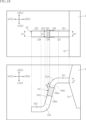
- the upper part is a partial enlarged view of FIG. 12, and the lower part is a partial enlarged view of FIG. 14.
- FIG. 13 shows the sealing resin 5 through the transparent resin for ease of understanding.
- the transparent sealing resin 5 is shown by an imaginary line (two-dot chain line). Note that in the drawings from FIG. 12 onwards, elements that are the same as or similar to those of the semiconductor device A1 of the above embodiment are given the same reference numerals as those of the above embodiment, and descriptions thereof will be omitted as appropriate.
- the arrangement of the first partition portion 226 in the first outer lead 22 and the arrangement of the fourth partition portion 236 in the second outer lead 23 differ from the semiconductor device A1 of the above embodiment.
- the first partition portion 226 is entirely provided in the first extension portion 223.
- both the boundary between the first partition portion 226 and the second partition portion 227 (first partition boundary 226a) and the boundary between the first partition portion 226 and the third partition portion 228 (second partition boundary 226b) are located in the first extension portion 223.
- the distance (third distance d3) between the first boundary 2201, which is the boundary between the first bend portion 224 and the first extension portion 223, and the first partition boundary 226a is, for example, 0.01 mm or more and 1.0 mm or less, and preferably 0.01 mm or more and 0.05 mm or less.
- the third distance d3 between the first boundary 2201 and the first partition boundary 226a is 1/20 to 1/2 times, and preferably 1/10 to 1/4 times, the dimension t1 in the thickness direction z of the first root portion 221. Note that the first partition portion 226 is hatched in FIG. 18.
- the fourth partition 236 is entirely provided in the second extension portion 233.
- both the boundary between the fourth partition 236 and the fifth partition 237 (third partition boundary 236a) and the boundary between the fourth partition 236 and the sixth partition 238 (fourth partition boundary 236b) are located in the second extension portion 233.
- the distance (fourth distance d4) between the second boundary 2301, which is the boundary between the third bend 234 and the second extension portion 233, and the third partition boundary 236a is, for example, 0.01 mm or more and 1.0 mm or less, and preferably 0.01 mm or more and 0.05 mm or less.
- the boundaries (first partition boundary 226a and second partition boundary 226b) between the first partition 226, which has a large width (dimension in the second direction y), and the second partition 227 and third partition 228, which are connected to it and have a small width (dimension in the second direction y), are located in the first extension 223, and are located away from the first bent portion 224.
- the distance (third distance d3) between the first boundary 2201, which is the boundary between the first bent portion 224 and the first extending portion 223, and the first partition boundary 226a, as viewed in the second direction y, is 0.01 mm or more and 1.0 mm or less.
- the third distance d3 between the first boundary 2201 and the first partition boundary 226a is 1/20 times or more and 1/2 times or less the dimension t1 in the thickness direction z of the first root portion 221.
- the boundaries (third partition boundary 236a and fourth partition boundary 236b) between the fourth partition 236, which has a large width (dimension in the second direction y), and the fifth partition 237 and sixth partition 238, which are connected to it and have small widths (dimension in the second direction y), are located in the second extension portion 233, and are located away from the third bend 234.
- the third partition boundary 236a and the fourth partition boundary 236b which are in portions with different widths (dimension in the second direction y), at positions that avoid the third bend 234, it is possible to stabilize the shape of the third bend 234 (second outer lead 23) after bending.
- the distance (fourth distance d4) between the second boundary 2301, which is the boundary between the third bent portion 234 and the second extending portion 233, and the third partition boundary 236a, as viewed in the second direction y, is 0.01 mm or more and 1.0 mm or less.
- the fourth distance d4 between the second boundary 2301 and the third partition boundary 236a is 1/20 times or more and 1/2 times or less the dimension t2 in the thickness direction z of the second root portion 231.
- Appendix 1 one or more semiconductor devices; A conductive support member; a sealing resin having a first resin side surface facing one side in a first direction perpendicular to the thickness direction and covering the one or more semiconductor elements; the conductive support member includes one or more first outer leads each having a first root portion extending in the first direction from the first resin side surface, a first mounting portion located on one side of the first root portion in the thickness direction, and a first extension portion connected to the first root portion via a first bent portion and connected to the first mounting portion via a second bent portion; the first outer lead includes a first partition portion including the first extension portion, a second partition portion including the first root portion and connected to the first partition portion, and a third partition portion including the first mounting portion and connected to the first partition portion, a dimension of the first partition in the thickness direction and a dimension of the second direction perpendicular to the first direction are greater than a dimension of the second partition in the second direction and a dimension of the third partition in the second
- the sealing resin has a second resin side surface facing the other side in the first direction
- the conductive support member includes one or more second outer leads each having a second root portion extending in the first direction from the second resin side surface, a second mounting portion located on one side of the second root portion in the thickness direction, and a second extension portion connected to the second root portion via a third bend portion and connected to the second mounting portion via a fourth bend portion;
- the second outer lead includes a fourth partition including the second extension portion, a fifth partition including the second root portion and connected to the fourth partition, and a sixth partition including the second mounting portion and connected to the fourth partition, a dimension of the fourth partition in the second direction is greater than a dimension of the fifth partition in the second direction and a dimension of the sixth partition in the second direction;
- a third partition boundary which is a boundary between the fourth partition portion and the fifth partition portion
- a fourth partition boundary which is a boundary between the fourth partition portion and the sixth partition portion
- Appendix 8. The semiconductor device of claim 7, wherein the third partition boundary is located at the second root portion and the fourth partition boundary is located at the second extension portion.
- Appendix 9. The semiconductor device described in Appendix 8, wherein, when viewed in the second direction, a second distance between a second boundary that is a boundary between the third bend portion and the second extension portion and the fourth partition boundary is 0.01 mm or more and 1.0 mm or less. Appendix 10.
- a second distance between a second boundary that is a boundary between the third bend portion and the second extension portion and the fourth partition boundary is greater than or equal to 1/20 and less than or equal to 1/2 of the dimension of the second root portion in the thickness direction.
- Appendix 11. 8. The semiconductor device according to claim 7, wherein the third partition boundary and the fourth partition boundary are located on the second extension portion.
- the conductive support member includes a plurality of the second outer leads, 12. The semiconductor device according to claim 7, wherein the second outer leads are arranged at intervals from each other in the second direction and overlap each other when viewed in the second direction. Appendix 13. 8.
- the conductive support member includes a die pad portion on which the one or more semiconductor elements are mounted.
- Appendix 14. the conductive support member is covered with the sealing resin and includes one or more first inner leads extending from each of the one or more first outer leads; 14. The semiconductor device according to claim 13, wherein at least one of the one or more first inner leads is electrically connected to the one or more semiconductor elements.
- Appendix 15. the conductive support member is covered with the sealing resin and includes one or more second inner leads extending from each of the one or more second outer leads; 15. The semiconductor device according to claim 14, wherein at least one of the one or more second inner leads is electrically connected to the one or more semiconductor elements.
- the die pad portion has a first die pad arranged on one side in the first direction and a second die pad arranged on the other side in the first direction and separated from the first die pad in the first direction, the one or more semiconductor elements include a first semiconductor element mounted on the first die pad and a second semiconductor element mounted on the second die pad; At least one of the one or more first inner leads is electrically connected to the first semiconductor element; 16. The semiconductor device according to claim 15, wherein at least one of the one or more second inner leads is electrically connected to the second semiconductor element.
- A1 A11: Semiconductor device 10: Semiconductor element 11: First semiconductor element 111: Electrode 12: Insulating element 121: First electrode 122: Second electrode 13: Second semiconductor element 131: Electrode 2: Conductive support member 21: Die pad portion 21A: First die pad 21B: Second die pad 211: Mounting surface 212: Through hole 22: First outer lead 22A: One end side first outer lead 22B: other end side first outer lead 22C: intermediate first outer lead 221: first root portion 222: first mounting portion 223: first extending portion 224: first bent portion 225: second bent portion 226: first partition portion 226a: first partition boundary 226b: second partition boundary 227: second partition portion 228: third partition portion 2201: first boundary 23: second outer lead 23A: one end side second outer lead 23B: other end side second outer lead 23C: intermediate second outer lead 231: second root portion 232: second mounting portion 233: second extending portion 234: third bent portion 235: fourth bent portion 236: fourth partition portion 236a
Landscapes
- Structures Or Materials For Encapsulating Or Coating Semiconductor Devices Or Solid State Devices (AREA)
Abstract
Description
図1~図10に基づき、本開示の第1実施形態に係る半導体装置A1について説明する。本実施形態の半導体装置A1は、2つの半導体素子10、絶縁素子12、導電支持部材2、複数のワイヤ31~34および封止樹脂5を備える。これらのうち導電支持部材2は、ダイパッド部21、複数の第1アウターリード22、複数の第2アウターリード23、複数の第1インナーリード24および複数の第2インナーリード25を含む。半導体装置A1の具体的な用途等は、何ら限定されないが、たとえば電気自動車またはハイブリッド自動車などのインバータ装置の配線基板に表面実装されるものである。半導体装置A1のパッケージ形式は、SOP(Small Outline Package)である。ただし、半導体装置A1のパッケージ形式は、SOPに限定されない。
図12~図19は、第1実施形態の第1変形例に係る半導体装置を示している。図12および図13は、本変形例の半導体装置A11を示す平面図である。図14は、半導体装置A11を示す正面図である。図15は、半導体装置A11を示す左側面図である。図16は、半導体装置A11を示す背面図である。図17は、半導体装置A11を示す右側面図である。図18および図19は、上段が図12の部分拡大図であり、下段が図14の部分拡大図である。なお、図13は、理解の便宜上、封止樹脂5を透過している。図13においては、透過した封止樹脂5を想像線(二点鎖線)で示している。なお、図12以降の図面において、上記実施形態の半導体装置A1と同一または類似の要素には、上記実施形態と同一の符号を付しており、適宜説明を省略する。
付記1.
1以上の半導体素子と、
導電支持部材と、
厚さ方向に直交する第1方向の一方側を向く第1樹脂側面を有し、前記1以上の半導体素子を覆う封止樹脂と、を備え、
前記導電支持部材は、前記第1樹脂側面から前記第1方向に延びる第1根元部と、前記第1根元部よりも前記厚さ方向の一方側に位置する第1実装部と、第1屈曲部を介して前記第1根元部につながり、且つ第2屈曲部を介して前記第1実装部につながる第1延出部と、を各々が有する1以上の第1アウターリードと、を含み、
前記第1アウターリードは、前記第1延出部を含む第1区画部と、前記第1根元部を含み、且つ前記第1区画部につながる第2区画部と、前記第1実装部を含み、且つ前記第1区画部につながる第3区画部と、を含み、
前記第1区画部の前記厚さ方向および前記第1方向に直交する第2方向の寸法は、前記第2区画部の前記第2方向の寸法、および前記第3区画部の前記第2方向の寸法よりも大であり、
前記第1区画部と前記第2区画部との境界である第1区画境界、および前記第1区画部と前記第3区画部との境界である第2区画境界の少なくとも一方は、前記第1延出部に位置する、半導体装置。
付記2.
前記第1区画境界が前記第1根元部に位置し、前記第2区画境界が前記第1延出部に位置する、付記1に記載の半導体装置。
付記3.
前記第2方向に見て、前記第1屈曲部と前記第1延出部との境界である第1境界と、前記第2区画境界との距離である第1距離は、0.01mm以上1.0mm以下である、付記2に記載の半導体装置。
付記4.
前記第2方向に見て、前記第1屈曲部と前記第1延出部との境界である第1境界と、前記第2区画境界との距離である第1距離は、前記第1根元部の前記厚さ方向の寸法の1/20倍以上1/2倍以下である、付記2または3に記載の半導体装置。
付記5.
前記第1区画境界および前記第2区画境界が前記第1延出部に位置する、付記1に記載の半導体装置。
付記6.
前記導電支持部材は、複数の前記第1アウターリードを含み、
当該複数の前記第1アウターリードは、前記第2方向において互いに間隔を隔てて配置され、且つ前記第2方向に見て互いに重なる、付記1ないし5のいずれかに記載の半導体装置。
付記7.
前記封止樹脂は、前記第1方向の他方側を向く第2樹脂側面を有し、
前記導電支持部材は、前記第2樹脂側面から前記第1方向に延びる第2根元部と、前記第2根元部よりも前記厚さ方向の一方側に位置する第2実装部と、第3屈曲部を介して前記第2根元部につながり、且つ第4屈曲部を介して前記第2実装部につながる第2延出部と、を各々が有する1以上の第2アウターリードを含み、
前記第2アウターリードは、前記第2延出部を含む第4区画部と、前記第2根元部を含み、且つ前記第4区画部につながる第5区画部と、前記第2実装部を含み、且つ前記第4区画部につながる第6区画部と、を含み、
前記第4区画部の前記第2方向の寸法は、前記第5区画部の前記第2方向の寸法、および前記第6区画部の前記第2方向の寸法よりも大であり、
前記第4区画部と前記第5区画部との境界である第3区画境界、および前記第4区画部と前記第6区画部との境界である第4区画境界の少なくとも一方は、前記第2延出部に位置する、付記1ないし6のいずれかに記載の半導体装置。
付記8.
前記第3区画境界が前記第2根元部に位置し、前記第4区画境界が前記第2延出部に位置する、付記7に記載の半導体装置。
付記9.
前記第2方向に見て、前記第3屈曲部と前記第2延出部との境界である第2境界と、前記第4区画境界との距離である第2距離は、0.01mm以上1.0mm以下である、付記8に記載の半導体装置。
付記10.
前記第2方向に見て、前記第3屈曲部と前記第2延出部との境界である第2境界と、前記第4区画境界との距離である第2距離は、前記第2根元部の前記厚さ方向の寸法の1/20倍以上1/2倍以下である、付記8または9に記載の半導体装置。
付記11.
前記第3区画境界および前記第4区画境界が前記第2延出部に位置する、付記7に記載の半導体装置。
付記12.
前記導電支持部材は、複数の前記第2アウターリードを含み、
当該複数の前記第2アウターリードは、前記第2方向において互いに間隔を隔てて配置され、且つ前記第2方向に見て互いに重なる、付記7ないし11のいずれかに記載の半導体装置。
付記13.
前記導電支持部材は、前記1以上の半導体素子が搭載されたダイパッド部を含む、付記7に記載の半導体装置。
付記14.
前記導電支持部材は、前記封止樹脂に覆われ、且つ前記1以上の第1アウターリードの各々から延びる1以上の第1インナーリードを含み、
前記1以上の第1インナーリードの少なくともいずれかは、前記1以上の半導体素子に導通する、付記13に記載の半導体装置。
付記15.
前記導電支持部材は、前記封止樹脂に覆われ、且つ前記1以上の第2アウターリードの各々から延びる1以上の第2インナーリードを含み、
前記1以上の第2インナーリードの少なくともいずれかは、前記1以上の半導体素子に導通する、付記14に記載の半導体装置。
付記16.
前記ダイパッド部は、前記第1方向の一方側に配置された第1ダイパッドと、前記第1方向の他方側に配置され、且つ前記第1方向において前記第1ダイパッドと離隔する第2第ダイパッドと、を有し、
前記1以上の半導体素子は、前記第1ダイパッドに搭載された第1半導体素子と、前記第2ダイパッドに搭載された第2半導体素子と、を含み、
前記1以上の第1インナーリードの少なくともいずれかは、前記第1半導体素子に導通し、
前記1以上の第2インナーリードの少なくともいずれかは、前記第2半導体素子に導通する、付記15に記載の半導体装置。
11:第1半導体素子 111:電極
12:絶縁素子 121:第1電極
122:第2電極 13:第2半導体素子
131:電極 2:導電支持部材
21:ダイパッド部 21A:第1ダイパッド
21B:第2ダイパッド 211:搭載面
212:貫通孔 22:第1アウターリード
22A:一端側第1アウターリード
22B:他端側第1アウターリード
22C:中間第1アウターリード 221:第1根元部
222:第1実装部 223:第1延出部
224:第1屈曲部 225:第2屈曲部
226:第1区画部 226a:第1区画境界
226b:第2区画境界 227:第2区画部
228:第3区画部 2201:第1境界
23:第2アウターリード 23A:一端側第2アウターリード
23B:他端側第2アウターリード 23C:中間第2アウターリード
231:第2根元部 232:第2実装部
233:第2延出部 234:第3屈曲部
235:第4屈曲部 236:第4区画部
236a:第3区画境界 236b:第4区画境界
237:第5区画部 238:第6区画部
2301:第2境界 24:第1インナーリード
24A:一端側第1インナーリード
24B:他端側第1インナーリード
24C:中間第1インナーリード 25:第2インナーリード
25A:一端側第2インナーリード
25B:他端側第2インナーリード
25C:中間第2インナーリード 31,32,33,34:ワイヤ
5:封止樹脂 51:樹脂主面
52:樹脂裏面 53:第1樹脂側面
531:第1上部 532:第1下部
533:第1中間部 54:第2樹脂側面
541:第2上部 542:第2下部
543:第2中間部 55:第3樹脂側面
551:第3上部 552:第3下部
553:第3中間部 56:第4樹脂側面
561:第4上部 562:第4下部
563:第4中間部 81:リードフレーム
811:外枠 812A:第1ダイパッド
812B:第2ダイパッド 813:第1リード
814:第2リード 815:支持リード
816:ダムバー d1:第1距離
d2:第2距離 d3:第3距離
d4:第4距離 t1,t2:寸法
w1,w2,w3,w4,w5,w6:寸法
Claims (16)
- 1以上の半導体素子と、
導電支持部材と、
厚さ方向に直交する第1方向の一方側を向く第1樹脂側面を有し、前記1以上の半導体素子を覆う封止樹脂と、を備え、
前記導電支持部材は、前記第1樹脂側面から前記第1方向に延びる第1根元部と、前記第1根元部よりも前記厚さ方向の一方側に位置する第1実装部と、第1屈曲部を介して前記第1根元部につながり、且つ第2屈曲部を介して前記第1実装部につながる第1延出部と、を各々が有する1以上の第1アウターリードと、を含み、
前記第1アウターリードは、前記第1延出部を含む第1区画部と、前記第1根元部を含み、且つ前記第1区画部につながる第2区画部と、前記第1実装部を含み、且つ前記第1区画部につながる第3区画部と、を含み、
前記第1区画部の前記厚さ方向および前記第1方向に直交する第2方向の寸法は、前記第2区画部の前記第2方向の寸法、および前記第3区画部の前記第2方向の寸法よりも大であり、
前記第1区画部と前記第2区画部との境界である第1区画境界、および前記第1区画部と前記第3区画部との境界である第2区画境界の少なくとも一方は、前記第1延出部に位置する、半導体装置。 - 前記第1区画境界が前記第1根元部に位置し、前記第2区画境界が前記第1延出部に位置する、請求項1に記載の半導体装置。
- 前記第2方向に見て、前記第1屈曲部と前記第1延出部との境界である第1境界と、前記第2区画境界との距離である第1距離は、0.01mm以上1.0mm以下である、請求項2に記載の半導体装置。
- 前記第2方向に見て、前記第1屈曲部と前記第1延出部との境界である第1境界と、前記第2区画境界との距離である第1距離は、前記第1根元部の前記厚さ方向の寸法の1/20倍以上1/2倍以下である、請求項2または3に記載の半導体装置。
- 前記第1区画境界および前記第2区画境界が前記第1延出部に位置する、請求項1に記載の半導体装置。
- 前記導電支持部材は、複数の前記第1アウターリードを含み、
当該複数の前記第1アウターリードは、前記第2方向において互いに間隔を隔てて配置され、且つ前記第2方向に見て互いに重なる、請求項1ないし5のいずれかに記載の半導体装置。 - 前記封止樹脂は、前記第1方向の他方側を向く第2樹脂側面を有し、
前記導電支持部材は、前記第2樹脂側面から前記第1方向に延びる第2根元部と、前記第2根元部よりも前記厚さ方向の一方側に位置する第2実装部と、第3屈曲部を介して前記第2根元部につながり、且つ第4屈曲部を介して前記第2実装部につながる第2延出部と、を各々が有する1以上の第2アウターリードを含み、
前記第2アウターリードは、前記第2延出部を含む第4区画部と、前記第2根元部を含み、且つ前記第4区画部につながる第5区画部と、前記第2実装部を含み、且つ前記第4区画部につながる第6区画部と、を含み、
前記第4区画部の前記第2方向の寸法は、前記第5区画部の前記第2方向の寸法、および前記第6区画部の前記第2方向の寸法よりも大であり、
前記第4区画部と前記第5区画部との境界である第3区画境界、および前記第4区画部と前記第6区画部との境界である第4区画境界の少なくとも一方は、前記第2延出部に位置する、請求項1ないし6のいずれかに記載の半導体装置。 - 前記第3区画境界が前記第2根元部に位置し、前記第4区画境界が前記第2延出部に位置する、請求項7に記載の半導体装置。
- 前記第2方向に見て、前記第3屈曲部と前記第2延出部との境界である第2境界と、前記第4区画境界との距離である第2距離は、0.01mm以上1.0mm以下である、請求項8に記載の半導体装置。
- 前記第2方向に見て、前記第3屈曲部と前記第2延出部との境界である第2境界と、前記第4区画境界との距離である第2距離は、前記第2根元部の前記厚さ方向の寸法の1/20倍以上1/2倍以下である、請求項8または9に記載の半導体装置。
- 前記第3区画境界および前記第4区画境界が前記第2延出部に位置する、請求項7に記載の半導体装置。
- 前記導電支持部材は、複数の前記第2アウターリードを含み、
当該複数の前記第2アウターリードは、前記第2方向において互いに間隔を隔てて配置され、且つ前記第2方向に見て互いに重なる、請求項7ないし11のいずれかに記載の半導体装置。 - 前記導電支持部材は、前記1以上の半導体素子が搭載されたダイパッド部を含む、請求項7に記載の半導体装置。
- 前記導電支持部材は、前記封止樹脂に覆われ、且つ前記1以上の第1アウターリードの各々から延びる1以上の第1インナーリードを含み、
前記1以上の第1インナーリードの少なくともいずれかは、前記1以上の半導体素子に導通する、請求項13に記載の半導体装置。 - 前記導電支持部材は、前記封止樹脂に覆われ、且つ前記1以上の第2アウターリードの各々から延びる1以上の第2インナーリードを含み、
前記1以上の第2インナーリードの少なくともいずれかは、前記1以上の半導体素子に導通する、請求項14に記載の半導体装置。 - 前記ダイパッド部は、前記第1方向の一方側に配置された第1ダイパッドと、前記第1方向の他方側に配置され、且つ前記第1方向において前記第1ダイパッドと離隔する第2第ダイパッドと、を有し、
前記1以上の半導体素子は、前記第1ダイパッドに搭載された第1半導体素子と、前記第2ダイパッドに搭載された第2半導体素子と、を含み、
前記1以上の第1インナーリードの少なくともいずれかは、前記第1半導体素子に導通し、
前記1以上の第2インナーリードの少なくともいずれかは、前記第2半導体素子に導通する、請求項15に記載の半導体装置。
Priority Applications (4)
| Application Number | Priority Date | Filing Date | Title |
|---|---|---|---|
| JP2025527580A JPWO2024257543A1 (ja) | 2023-06-12 | 2024-05-16 | |
| CN202480037697.1A CN121312323A (zh) | 2023-06-12 | 2024-05-16 | 半导体装置 |
| DE112024002507.2T DE112024002507T5 (de) | 2023-06-12 | 2024-05-16 | Halbleiterbauteil |
| US19/410,050 US20260090404A1 (en) | 2023-06-12 | 2025-12-05 | Semiconductor device |
Applications Claiming Priority (2)
| Application Number | Priority Date | Filing Date | Title |
|---|---|---|---|
| JP2023-096057 | 2023-06-12 | ||
| JP2023096057 | 2023-06-12 |
Related Child Applications (1)
| Application Number | Title | Priority Date | Filing Date |
|---|---|---|---|
| US19/410,050 Continuation US20260090404A1 (en) | 2023-06-12 | 2025-12-05 | Semiconductor device |
Publications (1)
| Publication Number | Publication Date |
|---|---|
| WO2024257543A1 true WO2024257543A1 (ja) | 2024-12-19 |
Family
ID=93852078
Family Applications (1)
| Application Number | Title | Priority Date | Filing Date |
|---|---|---|---|
| PCT/JP2024/018091 Ceased WO2024257543A1 (ja) | 2023-06-12 | 2024-05-16 | 半導体装置 |
Country Status (5)
| Country | Link |
|---|---|
| US (1) | US20260090404A1 (ja) |
| JP (1) | JPWO2024257543A1 (ja) |
| CN (1) | CN121312323A (ja) |
| DE (1) | DE112024002507T5 (ja) |
| WO (1) | WO2024257543A1 (ja) |
Citations (3)
| Publication number | Priority date | Publication date | Assignee | Title |
|---|---|---|---|---|
| JP2011091194A (ja) * | 2009-10-22 | 2011-05-06 | Renesas Electronics Corp | 半導体装置の製造方法および電子装置の製造方法 |
| JP2014007269A (ja) * | 2012-06-25 | 2014-01-16 | Mitsubishi Electric Corp | 半導体装置の製造方法および半導体装置 |
| WO2022138067A1 (ja) * | 2020-12-25 | 2022-06-30 | ローム株式会社 | 半導体装置 |
Family Cites Families (1)
| Publication number | Priority date | Publication date | Assignee | Title |
|---|---|---|---|---|
| JP7527916B2 (ja) | 2020-09-29 | 2024-08-05 | ローム株式会社 | 半導体装置 |
-
2024
- 2024-05-16 CN CN202480037697.1A patent/CN121312323A/zh active Pending
- 2024-05-16 JP JP2025527580A patent/JPWO2024257543A1/ja active Pending
- 2024-05-16 DE DE112024002507.2T patent/DE112024002507T5/de active Pending
- 2024-05-16 WO PCT/JP2024/018091 patent/WO2024257543A1/ja not_active Ceased
-
2025
- 2025-12-05 US US19/410,050 patent/US20260090404A1/en active Pending
Patent Citations (3)
| Publication number | Priority date | Publication date | Assignee | Title |
|---|---|---|---|---|
| JP2011091194A (ja) * | 2009-10-22 | 2011-05-06 | Renesas Electronics Corp | 半導体装置の製造方法および電子装置の製造方法 |
| JP2014007269A (ja) * | 2012-06-25 | 2014-01-16 | Mitsubishi Electric Corp | 半導体装置の製造方法および半導体装置 |
| WO2022138067A1 (ja) * | 2020-12-25 | 2022-06-30 | ローム株式会社 | 半導体装置 |
Also Published As
| Publication number | Publication date |
|---|---|
| US20260090404A1 (en) | 2026-03-26 |
| DE112024002507T5 (de) | 2026-03-26 |
| JPWO2024257543A1 (ja) | 2024-12-19 |
| CN121312323A (zh) | 2026-01-09 |
Similar Documents
| Publication | Publication Date | Title |
|---|---|---|
| US9202765B2 (en) | Semiconductor device | |
| JP3847676B2 (ja) | パワー半導体装置 | |
| JP7792472B2 (ja) | 半導体装置 | |
| US7615854B2 (en) | Semiconductor package that includes stacked semiconductor die | |
| JP7649171B2 (ja) | 半導体装置 | |
| JP7615286B2 (ja) | 半導体装置 | |
| CN111354709B (zh) | 半导体装置及其制造方法 | |
| WO2008042932A2 (en) | Interdigitated leadfingers | |
| WO2022054550A1 (ja) | 半導体装置 | |
| CN110600457A (zh) | 半导体装置 | |
| JP4100332B2 (ja) | 電子装置およびその製造方法 | |
| JP7594950B2 (ja) | 半導体装置 | |
| JP2021082794A (ja) | 電子部品および電子装置 | |
| CN110892526B (zh) | 半导体装置的制造方法 | |
| JP7798800B2 (ja) | 半導体装置 | |
| JPH11251508A (ja) | 絶縁物封止型電子装置及びその製造方法 | |
| JP7641135B2 (ja) | 電子部品および半導体装置 | |
| CN121312323A (zh) | 半导体装置 | |
| WO2024135356A1 (ja) | 半導体装置 | |
| JP7837876B2 (ja) | 半導体装置 | |
| US20240030109A1 (en) | Semiconductor device | |
| WO2024257544A1 (ja) | 半導体装置 | |
| JP4246598B2 (ja) | 電力用半導体装置 | |
| WO2023176370A1 (ja) | 半導体素子および半導体装置 | |
| WO2023218959A1 (ja) | 半導体装置、および、半導体装置の製造方法 |
Legal Events
| Date | Code | Title | Description |
|---|---|---|---|
| 121 | Ep: the epo has been informed by wipo that ep was designated in this application |
Ref document number: 24823165 Country of ref document: EP Kind code of ref document: A1 |
|
| ENP | Entry into the national phase |
Ref document number: 2025527580 Country of ref document: JP Kind code of ref document: A |
|
| WWE | Wipo information: entry into national phase |
Ref document number: CN2024800376971 Country of ref document: CN Ref document number: 2025527580 Country of ref document: JP |
|
| WWE | Wipo information: entry into national phase |
Ref document number: 112024002507 Country of ref document: DE |
|
| WWP | Wipo information: published in national office |
Ref document number: 112024002507 Country of ref document: DE |