WO2024252842A1 - 記憶装置及びメモリシステム - Google Patents
記憶装置及びメモリシステム Download PDFInfo
- Publication number
- WO2024252842A1 WO2024252842A1 PCT/JP2024/017271 JP2024017271W WO2024252842A1 WO 2024252842 A1 WO2024252842 A1 WO 2024252842A1 JP 2024017271 W JP2024017271 W JP 2024017271W WO 2024252842 A1 WO2024252842 A1 WO 2024252842A1
- Authority
- WO
- WIPO (PCT)
- Prior art keywords
- voltage
- ferroelectric layer
- layer
- pulse
- ferroelectric
- Prior art date
- Legal status (The legal status is an assumption and is not a legal conclusion. Google has not performed a legal analysis and makes no representation as to the accuracy of the status listed.)
- Ceased
Links
Images







Classifications
-
- H—ELECTRICITY
- H10—SEMICONDUCTOR DEVICES; ELECTRIC SOLID-STATE DEVICES NOT OTHERWISE PROVIDED FOR
- H10B—ELECTRONIC MEMORY DEVICES
- H10B51/00—Ferroelectric RAM [FeRAM] devices comprising ferroelectric memory transistors
- H10B51/30—Ferroelectric RAM [FeRAM] devices comprising ferroelectric memory transistors characterised by the memory core region
-
- G—PHYSICS
- G11—INFORMATION STORAGE
- G11C—STATIC STORES
- G11C11/00—Digital stores characterised by the use of particular electric or magnetic storage elements; Storage elements therefor
- G11C11/21—Digital stores characterised by the use of particular electric or magnetic storage elements; Storage elements therefor using electric elements
- G11C11/22—Digital stores characterised by the use of particular electric or magnetic storage elements; Storage elements therefor using electric elements using ferroelectric elements
- G11C11/223—Digital stores characterised by the use of particular electric or magnetic storage elements; Storage elements therefor using electric elements using ferroelectric elements using MOS with ferroelectric gate insulating film
-
- G—PHYSICS
- G11—INFORMATION STORAGE
- G11C—STATIC STORES
- G11C11/00—Digital stores characterised by the use of particular electric or magnetic storage elements; Storage elements therefor
- G11C11/21—Digital stores characterised by the use of particular electric or magnetic storage elements; Storage elements therefor using electric elements
- G11C11/22—Digital stores characterised by the use of particular electric or magnetic storage elements; Storage elements therefor using electric elements using ferroelectric elements
- G11C11/225—Auxiliary circuits
- G11C11/2259—Cell access
-
- G—PHYSICS
- G11—INFORMATION STORAGE
- G11C—STATIC STORES
- G11C11/00—Digital stores characterised by the use of particular electric or magnetic storage elements; Storage elements therefor
- G11C11/21—Digital stores characterised by the use of particular electric or magnetic storage elements; Storage elements therefor using electric elements
- G11C11/22—Digital stores characterised by the use of particular electric or magnetic storage elements; Storage elements therefor using electric elements using ferroelectric elements
- G11C11/225—Auxiliary circuits
- G11C11/2273—Reading or sensing circuits or methods
-
- G—PHYSICS
- G11—INFORMATION STORAGE
- G11C—STATIC STORES
- G11C11/00—Digital stores characterised by the use of particular electric or magnetic storage elements; Storage elements therefor
- G11C11/21—Digital stores characterised by the use of particular electric or magnetic storage elements; Storage elements therefor using electric elements
- G11C11/22—Digital stores characterised by the use of particular electric or magnetic storage elements; Storage elements therefor using electric elements using ferroelectric elements
- G11C11/225—Auxiliary circuits
- G11C11/2275—Writing or programming circuits or methods
-
- G—PHYSICS
- G11—INFORMATION STORAGE
- G11C—STATIC STORES
- G11C11/00—Digital stores characterised by the use of particular electric or magnetic storage elements; Storage elements therefor
- G11C11/21—Digital stores characterised by the use of particular electric or magnetic storage elements; Storage elements therefor using electric elements
- G11C11/22—Digital stores characterised by the use of particular electric or magnetic storage elements; Storage elements therefor using electric elements using ferroelectric elements
- G11C11/225—Auxiliary circuits
- G11C11/2277—Verifying circuits or methods
-
- G—PHYSICS
- G11—INFORMATION STORAGE
- G11C—STATIC STORES
- G11C11/00—Digital stores characterised by the use of particular electric or magnetic storage elements; Storage elements therefor
- G11C11/21—Digital stores characterised by the use of particular electric or magnetic storage elements; Storage elements therefor using electric elements
- G11C11/22—Digital stores characterised by the use of particular electric or magnetic storage elements; Storage elements therefor using electric elements using ferroelectric elements
- G11C11/225—Auxiliary circuits
- G11C11/2295—Protection circuits or methods
-
- G—PHYSICS
- G11—INFORMATION STORAGE
- G11C—STATIC STORES
- G11C11/00—Digital stores characterised by the use of particular electric or magnetic storage elements; Storage elements therefor
- G11C11/21—Digital stores characterised by the use of particular electric or magnetic storage elements; Storage elements therefor using electric elements
- G11C11/22—Digital stores characterised by the use of particular electric or magnetic storage elements; Storage elements therefor using electric elements using ferroelectric elements
- G11C11/225—Auxiliary circuits
- G11C11/2297—Power supply circuits
-
- H—ELECTRICITY
- H10—SEMICONDUCTOR DEVICES; ELECTRIC SOLID-STATE DEVICES NOT OTHERWISE PROVIDED FOR
- H10B—ELECTRONIC MEMORY DEVICES
- H10B51/00—Ferroelectric RAM [FeRAM] devices comprising ferroelectric memory transistors
- H10B51/20—Ferroelectric RAM [FeRAM] devices comprising ferroelectric memory transistors characterised by the three-dimensional [3D] arrangements, e.g. with cells on different height levels
-
- H—ELECTRICITY
- H10—SEMICONDUCTOR DEVICES; ELECTRIC SOLID-STATE DEVICES NOT OTHERWISE PROVIDED FOR
- H10D—INORGANIC ELECTRIC SEMICONDUCTOR DEVICES
- H10D30/00—Field-effect transistors [FET]
- H10D30/01—Manufacture or treatment
- H10D30/021—Manufacture or treatment of FETs having insulated gates [IGFET]
- H10D30/0415—Manufacture or treatment of FETs having insulated gates [IGFET] of FETs having ferroelectric gate insulators
-
- H—ELECTRICITY
- H10—SEMICONDUCTOR DEVICES; ELECTRIC SOLID-STATE DEVICES NOT OTHERWISE PROVIDED FOR
- H10D—INORGANIC ELECTRIC SEMICONDUCTOR DEVICES
- H10D30/00—Field-effect transistors [FET]
- H10D30/60—Insulated-gate field-effect transistors [IGFET]
- H10D30/67—Thin-film transistors [TFT]
- H10D30/674—Thin-film transistors [TFT] characterised by the active materials
- H10D30/6755—Oxide semiconductors, e.g. zinc oxide, copper aluminium oxide or cadmium stannate
-
- H—ELECTRICITY
- H10—SEMICONDUCTOR DEVICES; ELECTRIC SOLID-STATE DEVICES NOT OTHERWISE PROVIDED FOR
- H10D—INORGANIC ELECTRIC SEMICONDUCTOR DEVICES
- H10D30/00—Field-effect transistors [FET]
- H10D30/60—Insulated-gate field-effect transistors [IGFET]
- H10D30/701—IGFETs having ferroelectric gate insulators, e.g. ferroelectric FETs
-
- H—ELECTRICITY
- H10—SEMICONDUCTOR DEVICES; ELECTRIC SOLID-STATE DEVICES NOT OTHERWISE PROVIDED FOR
- H10D—INORGANIC ELECTRIC SEMICONDUCTOR DEVICES
- H10D62/00—Semiconductor bodies, or regions thereof, of devices having potential barriers
- H10D62/80—Semiconductor bodies, or regions thereof, of devices having potential barriers characterised by the materials
- H10D62/83—Semiconductor bodies, or regions thereof, of devices having potential barriers characterised by the materials being Group IV materials, e.g. B-doped Si or undoped Ge
-
- H—ELECTRICITY
- H10—SEMICONDUCTOR DEVICES; ELECTRIC SOLID-STATE DEVICES NOT OTHERWISE PROVIDED FOR
- H10D—INORGANIC ELECTRIC SEMICONDUCTOR DEVICES
- H10D62/00—Semiconductor bodies, or regions thereof, of devices having potential barriers
- H10D62/80—Semiconductor bodies, or regions thereof, of devices having potential barriers characterised by the materials
- H10D62/875—Semiconductor bodies, or regions thereof, of devices having potential barriers characterised by the materials being semiconductor metal oxide, e.g. InGaZnO
-
- H—ELECTRICITY
- H10—SEMICONDUCTOR DEVICES; ELECTRIC SOLID-STATE DEVICES NOT OTHERWISE PROVIDED FOR
- H10D—INORGANIC ELECTRIC SEMICONDUCTOR DEVICES
- H10D64/00—Electrodes of devices having potential barriers
- H10D64/60—Electrodes characterised by their materials
- H10D64/66—Electrodes having a conductor capacitively coupled to a semiconductor by an insulator, e.g. MIS electrodes
- H10D64/68—Electrodes having a conductor capacitively coupled to a semiconductor by an insulator, e.g. MIS electrodes characterised by the insulator, e.g. by the gate insulator
- H10D64/689—Electrodes having a conductor capacitively coupled to a semiconductor by an insulator, e.g. MIS electrodes characterised by the insulator, e.g. by the gate insulator having ferroelectric layers
Definitions
- One embodiment of the present invention relates to a memory device and a memory system.
- one embodiment of the present invention relates to a memory device having a ferroelectric layer and a memory system having the memory device.
- Non-Patent Documents 1-3 are documents published after the filing of U.S. Provisional Application No. 63/506675, which claims priority under the Paris Convention in this application.
- the programming voltage used when programming data into memory cells and the erasing voltage used when erasing data from memory cells can cause degradation of the interfaces between the thin film stacks that make up the FeFET (for example, the interface between the silicon oxide layer on the silicon substrate and the ferroelectric layer), resulting in a problem of poor rewrite resistance (endurance characteristics).
- One of the objectives of the present invention is to provide a storage device with high endurance characteristics.
- the memory device comprises a semiconductor layer, a gate electrode facing the semiconductor layer, an insulating layer provided between the semiconductor layer and the gate electrode, and a ferroelectric layer containing hafnium oxide provided between the insulating layer and the gate electrode, and the thickness of the ferroelectric layer is greater than 3 nm and less than 7 nm.
- the memory device comprises an oxide semiconductor layer, a gate electrode facing the oxide semiconductor layer, and a ferroelectric layer containing hafnium oxide provided between the oxide semiconductor layer and the gate electrode, and the thickness of the ferroelectric layer is greater than 1 nm and less than 30 nm.
- the memory system includes a memory cell array in which memory cells each having a storage device are arranged in a matrix, and a control circuit that controls the memory cell array.
- the control circuit determines whether a program operation or an erase operation has been performed on the memory cell a predetermined number of times, and when it determines that the number of times has been performed has reached the predetermined number, executes a voltage supply operation to apply a first voltage of a first polarity and a second voltage of a second polarity opposite to the first polarity to the ferroelectric layer, the first voltage being greater than the maximum voltage in the program operation, and the second voltage being greater than the maximum voltage in the erase operation.
- the memory system includes a plurality of memory cell arrays in which memory devices are arranged in a matrix, and a control circuit that controls the plurality of memory cell arrays.
- the control circuit determines whether a bit error rate is equal to or greater than a predetermined probability after executing a program operation or an erase operation, and if it determines that the bit error rate is equal to or greater than the predetermined probability, executes a voltage supply operation to apply a first voltage of a first polarity and a second voltage of a second polarity opposite to the first polarity to the ferroelectric layer, the first voltage being greater than a maximum voltage in the program operation, and the second voltage being greater than a maximum voltage in the erase operation.
- FIG. 1 is a schematic cross-sectional view showing an FeFET according to one embodiment of the present invention. 4 is a sequence diagram showing a method for manufacturing an FeFET according to one embodiment of the present invention.
- FIG. 1 is a cross-sectional TEM image of a ferroelectric layer of an FeFET according to an embodiment of the present invention.
- FIG. 2 is a diagram showing the I d -V g characteristics of an FeFET according to one embodiment of the present invention.
- FIG. 2 illustrates the memory window (MW) of an FeFET according to one embodiment of the present invention.
- FIG. 2 is a diagram showing the endurance characteristics of an FeFET according to an embodiment of the present invention.
- FIG. 1 is a diagram showing changes in I d -V g characteristics when an FeFET according to an embodiment of the present invention is driven at a low voltage or a high voltage.
- FIG. 2 is a diagram showing changes in PV characteristics when an FeFET according to an embodiment of the present invention is driven at a low voltage or at a high voltage.
- FIG. 1 is a diagram showing a mechanism for narrowing the MW of an FeFET when the FeFET according to one embodiment of the present invention is driven at a high voltage.
- FIG. 1 is a diagram showing a mechanism for narrowing the MW of an FeFET when the FeFET according to one embodiment of the present invention is driven at a low voltage.
- FIG. 2 is a diagram showing an outline of the recovery operation after cycling for an FeFET according to an embodiment of the present invention.
- FIG. 11 is a diagram showing changes in I d -V g characteristics due to recovery operations after high-voltage driving and after low-voltage driving for an FeFET according to an embodiment of the present invention.
- FIG. 1 is a diagram showing endurance characteristics before and after a recovery operation for an FeFET according to an embodiment of the present invention.
- FIG. 2 is a diagram showing the polarity of a recovery pulse in a recovery operation after cycling for an FeFET according to an embodiment of the present invention.
- FIG. 2 is a diagram showing the polarity of a recovery pulse in a recovery operation after cycling for an FeFET according to an embodiment of the present invention.
- FIG. 11 is a diagram showing changes in I d -V g characteristics due to recovery operations after high-voltage driving and after low-voltage driving for an FeFET according to an embodiment of the present invention.
- FIG. 1 is
- FIG. 2 is a diagram showing the polarity of a recovery pulse in a recovery operation after cycling for an FeFET according to an embodiment of the present invention.
- FIG. 13 shows the polarity dependence of the recovery pulse for MW after recovery operation of an FeFET according to an embodiment of the present invention.
- FIG. 13 is a diagram showing the voltage dependence of a recovery pulse for MW after a recovery operation of an FeFET according to an embodiment of the present invention.
- FIG. 13 is a diagram showing the pulse width dependence of the recovery pulse for MW after a recovery operation of an FeFET according to an embodiment of the present invention.
- 1 is a schematic diagram of a memory chip according to an embodiment of the present invention
- 1 is a circuit diagram of a memory chip according to an embodiment of the present invention
- 1 is a schematic diagram of a memory system according to an embodiment of the present invention
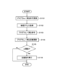
- 1 is a flowchart illustrating a recovery operation of a memory system according to an embodiment of the present invention
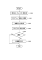
- 1 is a flowchart illustrating a recovery operation of a memory system according to an embodiment of the present invention.
- 1 shows the process flow for FeFETs with HZO film thicknesses of 4.6 nm, 6 nm, 8 nm, and 11 nm, and TEM images of HZO FeFETs with HZO film thicknesses of 4.6 nm and 11 nm.
- the driving voltage range is from -0.5 to 2 V to -2 to 3.5 V.
- Measurement condition: V D 50 mV.
- the driving voltage range is from -0.5 to 2 V to -2 to 3.5 V.
- Measurement condition: V D 50 mV.
- the driving voltage range is from -0.25 to 1.75 V to -1.5 to 3 V.
- Two MW narrowing mechanisms and proposed recovery signals (a) The recovery signal to V g for the FeFET with 4.6 nm HZO thickness is ⁇ 2 V/3 V, 20 s, and the recovery signal to V g for the other FeFET is ⁇ 2 V/3.5 V, 22 s. (b) Two MW narrowing mechanisms and proposed recovery signal; (c) Degradation mechanism due to high voltage cycling; Two MW narrowing mechanisms and proposed recovery signals. (c) Fast I d -V g initial, after cycling, and after high voltage (3.1 V/-2.1 V) recovery. Pulse duration is 1 ⁇ s. FeFETs with HZO thickness of 6 nm were used. Two MW narrowing mechanisms and the proposed recovery signal.
- the pulse duration is 1 ⁇ s. FeFETs with 6 nm HZO thickness were used. Two MW narrowing mechanisms and proposed recovery signals. (h) DC I d -V g initially, after cycling, and after low voltage (2.7 V/-1.7 V) recovery. The pulse duration is 1 ⁇ s. FeFETs with 6 nm HZO thickness were used. Two MW narrowing mechanisms and proposed recovery signals. (I) PV initial, after cycling, and after low voltage (2.7V/-1.7V) recovery. Pulse duration is 1 ⁇ s. FeFETs with 6 nm HZO thickness were used. (a) MW endurance characteristics in FeFETs with 11 nm HZO thickness after recovery pulses (three recovery cycles).
- FIG. 1 is a schematic cross-sectional view showing an FeFET according to one embodiment of the present invention.
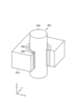
- 1 is a perspective view showing a configuration of a memory cell according to an embodiment of the present invention;
- FIG. 2 is a diagram showing a boundary between a high voltage in high-voltage driving and a low voltage in low-voltage driving for an FeFET according to an embodiment of the present invention.
- FIG. 2 is a diagram showing a boundary between a high voltage in high-voltage driving and a low voltage in low-voltage driving for an FeFET according to an embodiment of the present invention.
- the direction from the substrate toward the gate electrode is expressed as “above” and the opposite direction is expressed as “below”.
- the expressions “above” and “below” merely describe the hierarchical relationship of each element.
- the expression that a gate electrode is disposed above a substrate includes cases where other members are interposed between the substrate and the gate electrode.
- the expressions “above” and “below” include not only cases where the elements overlap in a planar view, but also cases where they do not overlap.
- the expressions “directly above” and “directly below” refer to cases where the elements overlap in a planar view.
- FIG. 1 to 19 the configuration of a memory device 10 according to an embodiment of the present invention will be described.
- a memory device 10 in which a ferroelectric layer 220 is used as a layer having a memory function is exemplified.
- the memory device 10 is a MOSFET in which the ferroelectric layer 220 is used as a gate insulating layer, and is called an "FeFET.”
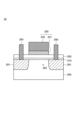
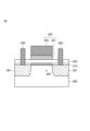
- FIG. 1 is a schematic cross-sectional view showing an FeFET according to an embodiment of the present invention.
- the memory device 10 has a semiconductor layer 200, an oxide insulating layer 210, a ferroelectric layer 220, a gate electrode 230, and an electrode 250.
- the semiconductor layer 200 may be a part (upper layer) of a semiconductor substrate, or may be a semiconductor layer formed on an insulating layer substrate such as SOI (Silicon on Insulator).
- SOI Silicon on Insulator
- the oxide insulating layer 210 is provided on the semiconductor layer 200.
- the ferroelectric layer 220 is provided on the oxide insulating layer 210.
- the oxide insulating layer 210 and the ferroelectric layer 220 may be collectively referred to as a gate insulating layer.
- the gate electrode 230 is provided on the ferroelectric layer 220.
- the gate electrode 230 includes a first conductive layer 231 and a second conductive layer 232.
- the gate electrode 230 has a two-layer structure, but the gate electrode 230 may have a one-layer structure or a three-layer or more structure.
- the above configuration can be expressed in other words as follows.
- the gate electrode 230 faces the semiconductor layer 200.
- the oxide insulating layer 210 is provided between the semiconductor layer 200 and the gate electrode 230.
- the ferroelectric layer 220 is provided between the oxide insulating layer 210 and the gate electrode 230.
- the oxide insulating layer 210 is also called an interface layer, and the semiconductor layer 200 is also called a channel layer.
- the semiconductor layer 200 is provided with a low resistance region 201 and a channel region 202.
- the low resistance region 201 is a region that does not overlap with the gate electrode 230 in a plan view.
- An impurity that reduces the resistance of the semiconductor layer 200 is introduced into the semiconductor layer 200 in the low resistance region 201.
- the semiconductor layer 200 contains silicon
- phosphorus (P) is used as the impurity
- boron (B) is used.
- the channel region 202 is a region sandwiched between two separated low resistance regions 201.
- One of the two low resistance regions 201 functions as a source region, and the other functions as a drain region.
- the semiconductor layer 200 in the channel region 202 has a property that it can be switched between an on state and an off state by a voltage supplied to the gate electrode 230.
- the oxide insulating layer 210 contacts the semiconductor layer 200 in the channel region 202.
- the thickness of the oxide insulating layer 210 is less than 5 nm, 3 nm or less, 2 nm or less, 1 nm or less, or 0.7 nm or less. In any case, the thickness of the oxide insulating layer 210 is greater than 0 nm.
- the oxide insulating layer 210 is, for example, a layer in which the semiconductor layer 200 is oxidized. When the semiconductor layer 200 is a silicon substrate, the oxide insulating layer 210 contains silicon oxide.
- the oxide insulating layer 210 is obtained by applying a mixed solution of hydrochloric acid, hydrogen peroxide, and water to the semiconductor layer 200, or by immersing the semiconductor layer 200 in the mixed solution. More specifically, the oxide insulating layer 210 is formed by an SC2 (Standard Clean 2) process included in the RCA cleaning. However, the oxide insulating layer 210 may be formed by thermal oxidation of the semiconductor layer 200.
- SC2 Standard Clean 2
- the ferroelectric layer 220 is a dielectric layer in which electric dipoles are aligned even when no electric field is applied from the outside.
- the ferroelectric layer 220 is a dielectric layer in which the direction of the electric dipoles changes when an electric field is applied from the outside.
- the threshold voltage in the I d -V g characteristic (I d : drain current, V g : gate voltage) of the memory device 10 shifts depending on the direction of the electric dipoles of the ferroelectric layer 220.
- the memory device 10 is used as a memory cell.
- a ferroelectric containing hafnium oxide is used as the ferroelectric layer 220.
- a mixed crystal of hafnium oxide and zirconium oxide (HZO; Hf 0.5 Zr 0.5 O 2 ) is used as the ferroelectric layer 220.
- the ferroelectric layer 220 is in contact with the oxide insulating layer 210.
- the thickness of the ferroelectric layer 220 is greater than 3 nm and less than 7 nm, or is 4.6 nm or more and 6 nm or less.
- the ferroelectric layer 220 may contain at least any of silicon, magnesium, aluminum, barium, zirconium, gadolinium, lanthanum, samarium, nitrogen, and yttrium.
- the gate electrode 230 is an electrode to which a voltage (gate voltage) for switching the memory device 10 between the on state and the off state, or a voltage (program voltage or erase voltage) for changing the orientation of the electric dipole of the ferroelectric layer 220 is supplied.
- a voltage gate voltage
- tungsten tungsten nitride
- ruthenium ruthenium oxide
- ruthenium oxide can be used as the first conductive layer 231.
- Aluminum and polycrystalline silicon can be used as the second conductive layer 232.
- Electrodes are provided in the oxide insulating layer 210 and the ferroelectric layer 220.
- the contacts reach the low resistance region 201 of the semiconductor layer 200.
- An electrode 250 is formed by depositing a conductive layer inside the contact.
- the electrode connected to the source region is the source electrode
- the electrode connected to the drain region is the drain electrode.
- a general metal material is used for the electrode 250.
- tungsten which can be deposited by a CVD (Chemical Vapor Deposition) method, is used for the electrode 250.
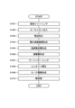
- [1-2. Manufacturing method of the storage device 10] 2 is a sequence diagram showing a method for manufacturing an FeFET according to an embodiment of the present invention.
- substrate cleaning is performed on a substrate including a semiconductor layer 200 (step S1001; substrate cleaning).
- RCA cleaning is performed as the substrate cleaning.
- the RCA cleaning is cleaning including an SC1 process (Standard Clean 1) and the above-mentioned SC2 process.
- SC1 process is a process in which a mixed solution of ammonium hydroxide water, hydrogen peroxide water, and water is applied to the semiconductor layer 200, or the semiconductor layer 200 is immersed in the mixed solution.
- a mask is formed by a photolithography process, in which the regions that will become the low resistance regions 201 in a later step are opened, and impurity ions are implanted into the semiconductor layer 200 in the opened regions (step S1002; S/D ion implantation).
- step S1003 thermal activation of the implanted impurities is performed (step S1003; thermal activation).
- the thermal activation in S1003 is performed, for example, by heat treatment at 1000°C.
- an SC2 treatment is performed on the surface of the semiconductor layer 200.
- This SC2 treatment forms an oxide insulating layer 210 on the surface of the semiconductor layer 200 (step S1004; Formation of oxide insulating layer).
- the oxide insulating layer 210 is formed by oxidation using such a chemical solution (chemical oxidation)
- the thickness of the formed oxide insulating layer 210 is very thin. Details will be described later, but in this embodiment, the thickness of the formed oxide insulating layer 210 is approximately 0.7 nm.
- the ferroelectric layer 220 is formed on the oxide insulating layer 210 (step S1005; ferroelectric layer formation).
- the ferroelectric layer 220 is formed, for example, by atomic layer deposition (ALD). However, the ferroelectric layer 220 may be formed by other methods.
- the first conductive layer 231 and the second conductive layer 232 (gate electrode 230) are formed on the ferroelectric layer 220 (step S1006; conductive layer formation).
- a mask is formed on the conductive layer formed in S1006, and the conductive layer is etched through the mask to form a pattern of the gate electrode 230 (step S1007; gate patterning).
- the ferroelectric layer 220 is exposed except for the area where the pattern of the gate electrode 230 is formed.
- step S1008 contact opening
- a conductive layer is formed inside the contact to form the electrode 250 (step S1009; S/D electrode formation).
- step S1010 heat treatment
- the heat treatment is performed, for example, at 400° C. for 30 seconds.
- the manufacturing method in which ion implantation in S1002 is performed before forming the oxide insulating layer 210 is exemplified, but the manufacturing method is not limited to this.
- ion implantation may be performed in the semiconductor layer 200 using the gate pattern as a mask.
- FIG. 3 is a cross-sectional TEM image of the ferroelectric layer of an FeFET according to one embodiment of the present invention. Four cross-sectional TEM images are shown in FIG. 3. In FIG. 3, the cross-sectional TEM images are of the memory device 10 in which the thicknesses of the ferroelectric layer 220 are 11 nm, 8 nm, 6 nm, and 4.6 nm from the left. From the cross-sectional TEM image shown in FIG.
- the thickness of the ferroelectric layer 220 used in this embodiment is almost the same as the above numerical value, and that the ferroelectric layer 220 exhibits good crystallinity.
- the thickness of the oxide insulating layer 210 is about 0.7 nm.
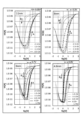
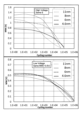
- FIG. 4 is a diagram showing the I d -V g characteristic of an FeFET according to an embodiment of the present invention.
- the four graphs shown in FIG. 4 are I d -V g characteristics measured for four types of memory devices 10 having different film thicknesses of the ferroelectric layer 220.
- V g is the voltage applied to the gate electrode 230.
- I d is the current flowing between the electrode 250 functioning as the source electrode and the electrode 250 functioning as the drain electrode.
- the distance (channel length) between the low resistance region 201 functioning as the source region and the low resistance region 201 functioning as the drain region is 10 ⁇ m, and the channel width perpendicular to the channel length is 100 ⁇ m.
- the drain voltage between the electrodes 250 during the measurement of the I d -V g characteristic is 0.05 V.
- the I d -V g characteristic shown in FIG. 4 is obtained by scanning V g while a voltage is continuously applied to the gate electrode 230, and when a high voltage is applied to V g , polarization inversion occurs in the ferroelectric layer 220.
- Such an I d -V g characteristic is sometimes called "DC I d -V g ".
- I d -V g characteristics with different gate voltage scan ranges are displayed.
- I d -V g characteristics are displayed when the gate voltage scan ranges are "-2 to 3.5 V (thin dotted line)", “-1.5 to 3 V (thin dashed line)", “-1 to 2.5 V (thin solid line)", and " -0.5 to 2 V (thick dashed line)".
- I d -V g characteristics are displayed when the scan range of the gate voltage is "-2 to 3.5 V (thin dotted line)", “-1.5 to 3 V (thin dashed line)", “-1 to 2.5 V (thin solid line)", “-0.5 to 2 V (thick dashed line)", and "-0.25 to 1.75 V (thick solid line)".
- I d -V g characteristics are displayed when the scan range of the gate voltage is "-1.5 to 3 V (thin dashed line)", “-1 to 2.5 V (thin solid line)", “-0.5 to 2 V (thick dashed line)", and "-0.25 to 1.75 V (thick solid line)".
- the measurement of the I d -V g characteristic shown in FIG. 4 is performed by first scanning in the direction from the minimum value to the maximum value (forward direction; A) in each scanning range, then turning back at the maximum value, and scanning in the direction from the maximum value to the minimum value (reverse direction; B).
- a minimum voltage negative maximum voltage
- V g the electric dipole of the ferroelectric layer 220 is polarized so that the positive charge approaches the gate electrode 230.
- the voltage applied to V g changes from a negative voltage to a positive voltage, and V g becomes larger than a predetermined positive voltage, the direction of the electric dipole is reversed.
- the threshold voltage of the I d -V g characteristic (for example, V g when I d is 10 -6 A) differs between the forward and reverse directions. This difference in threshold voltage is called the memory window (MW).
- the MW at each film thickness of the ferroelectric layer 220 is evaluated for the gate voltage scan range of "-0.25 to 1.75 V (thick solid line)"
- the MW is approximately 0.5 V
- the film thickness of the ferroelectric layer 220 is 8 nm and 11 nm
- the MW is zero. Therefore, in the memory device 10 in which the film thickness of the ferroelectric layer 220 is 11 nm (top left graph) and 8 nm (top right graph), the I d -V g characteristics shown by the thick solid line are not displayed.
- the thickness of the ferroelectric layer 220 is less than 7 nm, sufficient MW can be obtained even in the low voltage range of -0.5 to 2 V.
- the thickness of the ferroelectric layer 220 is greater than 3 nm.
- the film thickness of the ferroelectric layer 220 In order to reduce the absolute values of the program voltage and erase voltage of the memory device 10, it is necessary to reduce the film thickness of the ferroelectric layer 220. However, as described above, taking into consideration the performance required of the memory device 10, it is preferable that the film thickness of the ferroelectric layer 220 be greater than 3 nm and less than 7 nm.
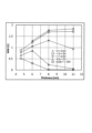
- FIG. 5 is a diagram showing the memory window (MW) of an FeFET according to one embodiment of the present invention.
- the plot shown in FIG. 5 is the MW calculated from the graph in FIG. 4.
- the MW when the gate voltage scan range in FIG. 4 is "-2 to 3.5 V (thin dotted line)" is shown by “x” in FIG. 5.
- the MW when the gate voltage scan range in FIG. 4 is “-1.5 to 3 V (thin dashed line)” is shown by “ ⁇ ” in FIG. 5.
- the MW when the gate voltage scan range in FIG. 4 is “-1 to 2.5 V (thin solid line)” is shown by " ⁇ ” in FIG. 5.
- the MW when the gate voltage scan range in FIG. 5 is a diagram showing the memory window (MW) of an FeFET according to one embodiment of the present invention.
- the plot shown in FIG. 5 is the MW calculated from the graph in FIG. 4.
- the effect that the MW can be secured even if the film thickness of the ferroelectric layer 220 is thin and the scan range is low voltage as described above is an effect that is first recognized in the unique range where the film thickness of the ferroelectric layer 220 is greater than 3 nm and less than 7 nm, and the scan range of the gate voltage is "-0.5 to 2 V".
- This effect is particularly noticeable when the film thickness of the ferroelectric layer 220 is 4.6 nm or more and 6 nm or less, and the gate voltage scan range is "-0.25 to 1.75 V.”
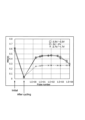
- FIG. 6 is a diagram showing the endurance characteristics of an FeFET according to an embodiment of the present invention.
- the two graphs in FIG. 6 each show the endurance characteristics of the memory device 10 when cycled.
- the horizontal axis shows the number of cycles (Cycling number), and the vertical axis shows MW.
- cycle driving pulse voltages (positive pulse voltage and negative pulse voltage) corresponding to program operation and erase operation are repeatedly applied to the memory device 10.
- the positive pulse voltage and the negative pulse voltage are applied to the gate electrode 230 with 0V applied to the electrode 250, respectively.
- the pulse width of these pulse voltages is 1 ⁇ sec.
- the two graphs in FIG. 6 show different cycle driving conditions.
- the upper graph labeled "High Voltage Same E” shows the endurance characteristics when cycle driving is performed at a relatively high voltage (the voltage shown in Table 1 below).
- the graph below, labeled “Low Voltage Same MW ( ⁇ 0.5V),” shows the endurance characteristics when cycle driving is performed at a relatively low voltage (the voltage shown in Table 2 below).
- the driving period from the start of cycle driving until MW becomes zero is referred to as the number of cycles.
- the pulse voltage is adjusted so that the electric field intensity in the ferroelectric layer 220 is constant in order to suppress the influence of the electric field applied to the ferroelectric layer 220.
- a neutral voltage is obtained from a region where the polarization is not reversed, and the electric field intensity related to the ferroelectric layer 220 is obtained by dividing the potential difference from the neutral voltage by the film thickness of the ferroelectric layer 220.
- the neutral voltage is a voltage at the midpoint between the voltage at which the polarization becomes zero when the gate voltage Vg is scanned from a negative voltage to a positive voltage, and the voltage at which the polarization becomes zero when the gate voltage Vg is scanned from a positive voltage to a negative voltage, in the P-V characteristic shown in FIG. 8 described later, for example.
- the "positive pulse voltage/negative pulse voltage” for the film thickness of the ferroelectric layer 220 is as shown in Table 1.
- the term "high voltage driving" or “high voltage cycle” means that the voltages shown in Table 1 are applied to the respective film thicknesses of the ferroelectric layer 220.
- the "positive pulse voltage/negative pulse voltage” for each thickness of the ferroelectric layer 220 is as shown in Table 2.
- “low voltage drive” or “low voltage cycle” means that the voltage shown in Table 2 is applied for each thickness of the ferroelectric layer 220.
- the number of cycles (the number of cycles when MW reaches 0 V) of the memory device 10 having the ferroelectric layer 220 with thicknesses of 8 nm and 11 nm is about 5 x 10⁴ cycles, whereas the number of cycles of the memory device 10 having the ferroelectric layer 220 with thicknesses of 4.6 nm and 6 nm is about 105 cycles. Furthermore, as shown in the lower graph of Fig. 6, the number of cycles of the memory device 10 having the ferroelectric layer 220 with thicknesses of 4.6 nm and 6 nm reaches 106 cycles.
- an endurance characteristic of about 105 cycles could be obtained even under relatively high voltage conditions. Furthermore, by reducing the pulse voltage applied to the memory device 10, an endurance characteristic of about 106 cycles could be obtained.
- the coercive voltage Vc is first derived from the P-V characteristics of the ferroelectric layer 220.
- the coercive voltage Vc is a voltage required for the polarization (electric dipole) to start switching from a state in which it faces a certain direction to a state in which it faces the opposite direction.
- the coercive voltage Vc corresponds to the difference between the neutral voltage and the voltage at which the polarization value rises from a negative value to zero when the gate voltage Vg is scanned from a negative voltage to a positive voltage in the P-V characteristics shown in FIG. 8, which will be described later, for example.
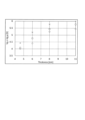
- Range of write voltage When the difference between the positive pulse voltage and the negative pulse voltage shown in Tables 1 and 2 is expressed as the "range of write voltage,” it has been confirmed that there is a rule that the boundary between high voltage and low voltage is specified by the value obtained by multiplying the coercive voltage Vc by a coefficient of 3.4. In other words, it has been confirmed that the relationship between the range of write voltages classified as high voltages and the coercive voltage Vc , and the relationship between the range of write voltages classified as low voltages and the coercive voltage Vc , based on the boundary, have the following rule. Range of write voltage classified as high voltage > 3.4 ⁇ Vc Range of write voltage classified as low voltage ⁇ 3.4 ⁇ Vc
- the vertical axis indicates the range of write voltages (Vg, n-Vg, p [V]), and the horizontal axis indicates the thickness (Thickness [nm]) of the ferroelectric layer 220.
- the range of write voltages classified as low voltages is indicated by “ ⁇ ” in Fig. 38
- the range of write voltages classified as high voltages is indicated by “X” in Fig. 38.
- Coercive voltage V c ⁇ 3.4 is indicated by " ⁇ " in Fig. 38.
- Fig. 38 the vertical axis indicates the range of write voltages (Vg, n-Vg, p [V])
- the horizontal axis indicates the thickness (Thickness [nm]) of the ferroelectric layer 220.
- the range of write voltages larger than coercive voltage V c ⁇ 3.4 " ⁇ " is classified as high voltages, and the range of write voltages smaller than coercive voltage V c ⁇ 3.4 " ⁇ " is classified as low voltages.
- x is the thickness (Thickness [nm]) of the ferroelectric layer 220
- y is the range of the write voltage (Vg, n-Vg, p [V]).
- the range of write voltages greater than the above formula (solid line in FIG. 39) is classified as high voltages, and the range of write voltages less than the above formula is classified as low voltages.
- the inventors discovered that the mechanism by which the MW is narrowed differs between when a memory cell is subjected to high-voltage cycle driving and when it is subjected to low-voltage cycle driving.
- the inventors clarified that the reason the MW becomes smaller when subjected to low-voltage cycle driving is due to fatigue of the ferroelectric layer, which is different from conventional technological common sense.
- the inventors established a method for recovering this fatigue of the ferroelectric layer, and succeeded in increasing the MW that had once become smaller due to cycle driving.
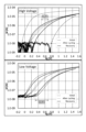
- FIG. 7 is a diagram showing the change in I d -V g characteristics when low-voltage driving or high-voltage driving is performed on the FeFET according to one embodiment of the present invention.
- the I d -V g characteristics shown in FIG. 7 are the I d -V g characteristics before the start of cycle driving (solid line; Initial) and the I d -V g characteristics after cycle driving (dashed line; After cycling).
- the upper graph in FIG. 7 shows the I d -V g characteristics before and after the high voltage cycle (High Voltage), and the lower graph shows the I d -V g characteristics before and after the low voltage cycle (Low Voltage).
- the I d -V g characteristics shown in FIG. 7 are evaluated by applying a pulse voltage of 1 ⁇ sec to the gate electrode 230 to change the direction of the electric dipole, and then performing a V g scan of 0.1 sec on the same gate electrode.
- the diagonal lines of the solid/dotted right-angled triangles in FIG. 7 indicate the slopes near the threshold voltage in the I d -V g characteristics before and after the cycle operation.
- the S value changes significantly with the narrowing of the MW.
- the S value after the high-voltage cycle is larger than that before the high-voltage cycle. In other words, the high-voltage cycle causes the current value in the I d -V g characteristics to rise more gently.
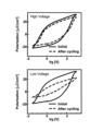
- FIG. 8 is a diagram showing the change in the P-V characteristics when the FeFET according to one embodiment of the present invention is driven at a low voltage or a high voltage.
- the P-V characteristics shown in FIG. 8 are the P-V characteristics before the start of the cycle drive (solid line; Initial) and the P-V characteristics after the cycle drive (dashed line; After cycling).
- the horizontal axis of the graph showing each P-V characteristic is the gate voltage V g [V], and the vertical axis is the polarization [ ⁇ C/cm 2 ].
- the upper graph (High Voltage) in FIG. 8 shows the P-V characteristics before and after the high voltage cycle
- the lower graph (Low Voltage) shows the P-V characteristics before and after the low voltage cycle.
- 8 is the PV characteristic of the memory device 10 in which the film thickness of the ferroelectric layer 220 is 6 nm.
- the pulse voltages in the high voltage cycle and the low voltage cycle are the same as the pulse voltages described in FIG.
- the pulse voltage applied to the memory device 10 by the high voltage cycle is the same as the pulse voltage for a conventional memory cell. Therefore, the narrowing of the MW caused by the high voltage cycle is considered to be caused by the trap level of charge ("x" in FIG. 9) generated at the interface between the semiconductor layer 200 and the oxide insulating layer 210 and the interface between the oxide insulating layer 210 and the ferroelectric layer 220, as shown in FIG. 9.
- FIG. 9 is a diagram showing the mechanism of narrowing of the MW of the FeFET when the FeFET according to the embodiment of the present invention is driven at a high voltage. As shown in FIG.
- FIG. 10 is a diagram showing the mechanism of narrowing of the MW of an FeFET when the FeFET according to one embodiment of the present invention is driven at a low voltage.
- the inventors have discovered that the mechanism by which MW narrowing occurs due to low-voltage cycles is different from the mechanism by which MW narrowing occurs due to high-voltage cycles. Furthermore, the inventors have clarified that the narrowing of MW due to low-voltage cycles is due to fatigue of the ferroelectric layer.
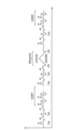
- FIG. 11 is a diagram showing an outline of the recovery operation after cycle driving for an FeFET according to one embodiment of the present invention.
- P indicates a positive pulse voltage corresponding to a program operation.
- R indicates an applied voltage corresponding to a read operation (measurement of fast I d -V g ).
- E indicates a negative pulse voltage corresponding to an erase operation. The pulse widths of the positive pulse voltage and the negative pulse voltage are both 1 ⁇ sec.
- Cycle 1 indicates the first cycle driving.
- Cycle 2 indicates the second cycle driving.
- “Recovery” indicates a recovery operation.
- the voltage is increased from -2 V to 3 V and decreased from 3 V to -2 V in 20 seconds. If the thickness of the ferroelectric layer 220 is 6 nm, 8 nm, or 11 nm, the voltage is increased from -2 V to 3.5 V and decreased from 3.5 V to -2 V in 22 seconds.
- the time for performing the recovery operation is on the order of seconds, but the recovery operation shown in FIG. 11 is a trial process, and the details will be described later, but in reality the recovery operation can be performed in a shorter time.
- the I d -V g characteristic of the initial state shown in FIG. 12, which will be described later, is obtained by the program operation, the erase operation, and the read operation after these operations, which are performed before the first cycle driving.
- the first cycle driving a positive pulse voltage and a negative pulse voltage are applied alternately, and the read operation is performed every predetermined number of times, thereby obtaining the endurance characteristic.
- the cycle driving ends when MW is determined to be zero in the endurance characteristic.
- the I d -V g characteristic of the after cycling state shown in FIG. 12, which will be described later, is obtained by the program operation, the erase operation, and the read operation after these operations, which are performed after the first cycle driving.
- the I d -V g characteristic of the after recovery operation shown in FIG. 12, which will be described later, is obtained by the program operation, the erase operation, and the read operation after these operations , which are performed after the recovery operation and before the second cycle driving. Thereafter, the second cycle driving is performed in the same manner as the first cycle driving.
- FIG. 12 is a diagram showing the change in I d -V g characteristics due to recovery operation after high voltage driving or low voltage driving for an FeFET according to an embodiment of the present invention.
- the I d -V g characteristics shown in FIG. 12 are the I d -V g characteristics before the start of cycle driving (thin solid line; Initial), the I d -V g characteristics after cycle driving (thin dashed line; After cycling), and the I d -V g characteristics after recovery operation (thick solid line; Recovery).
- the upper graph in FIG. 12 shows the I d -V g characteristics before and after the high voltage cycle (High Voltage), and the lower graph shows the I d -V g characteristics before and after the low voltage cycle (Low Voltage).
- the I d -V g characteristics shown in FIG. 12 are the I d -V g characteristics of a memory device 10 in which the film thickness of the ferroelectric layer 220 is 6 nm. That is, the positive pulse voltage in the high voltage cycle is 3.1 V and the negative pulse voltage is ⁇ 2.1 V. On the other hand, the positive pulse voltage in the low voltage cycle is 2.7 V and the negative pulse voltage is ⁇ 1.7 V.
- the I d -V g characteristics shown in Fig. 12 are fast I d -V g as in Fig. 7.
- the I d -V g characteristics before the start of cycling (Initial) and after cycling (After cycling) in the graph shown in Fig. 12 are the same as those shown in Fig. 7.
- MW is larger after the recovery operation (Recovery) in both the high voltage cycle and the low voltage cycle.
- the MW recovered by the recovery operation after the high voltage cycle is approximately 0.2 V.
- the MW recovered by the recovery operation after the low voltage cycle is approximately 0.4 V.
- the change in MW before and after the low voltage cycle is smaller than the change in MW before and after the high voltage cycle.
- the effect of the recovery operation is greater in the low voltage cycle.
- the narrowing of the MW caused by the low voltage cycle can be recovered by the above recovery operation.
- the fatigue of the ferroelectric layer 220 can be recovered by the above recovery operation.
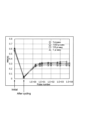
- FIG. 13 is a diagram showing the endurance characteristics after a recovery operation for an FeFET according to one embodiment of the present invention. All four endurance characteristics shown in FIG. 13 are endurance characteristics obtained based on the change in MW due to low-voltage cycles. In these graphs, the horizontal axis indicates the number of cycles (cycling number) and the vertical axis indicates MW. The four graphs are endurance characteristics for memory devices 10 with different film thicknesses of the ferroelectric layer 220. The upper left, upper right, lower left, and lower right graphs are endurance characteristics for memory devices 10 with ferroelectric layer 220 film thicknesses of 11 nm, 8 nm, 6 nm, and 4.6 nm, respectively.
- the voltages shown in Table 2 are applied as pulse voltages for each film thickness condition during cycle driving.
- Each graph shows the endurance characteristics during the first cycle driving (Cycle 1) (thin dashed line; Cycle 1), the endurance characteristics during the second cycle driving (Cycle 2) (thin solid line; Cycle 2), and the endurance characteristics during the third cycle driving (Cycle 3) (thick solid line; Cycle 3).
- the recovery operation shown in Figure 11 is performed between the first and second cycle driving and between the second and third cycle driving.
- the initial MW of cycle 2 and cycle 3 is less than half of the initial MW of cycle 1. Furthermore, the number of cycles in cycle 2 and cycle 3 is about one order of magnitude smaller than the number of cycles in cycle 1. In other words, under these conditions, even if the above recovery operation is performed, a sufficient recovery effect of the endurance characteristics cannot be obtained.
- the initial MW of cycle 2 and cycle 3 is about half of the initial MW of cycle 1. Furthermore, the number of cycles in cycle 2 and cycle 3 is smaller than the number of cycles in cycle 1. However, compared to the 11 nm condition, the number of cycles in cycle 2 and cycle 3 is greater. In other words, under these conditions, even if the above recovery operation is performed, a sufficient recovery effect in the endurance characteristics cannot be obtained, but a recovery effect can be obtained compared to the 11 nm condition.
- the initial MW of cycle 2 and cycle 3 is smaller than the initial MW of cycle 1.
- the initial MW of cycle 2 and cycle 3 is larger than the initial MW of cycle 2 and cycle 3 under the above-mentioned 11 nm and 8 nm conditions.
- the initial MW in cycle 2 and cycle 3 is smaller than the initial MW in cycle 1.
- the MW is less likely to decrease even if the number of cycles increases.
- the number of cycles in cycle 2 and cycle 3 is smaller than the number of cycles in cycle 1, the number of cycles in cycle 2 and cycle 3 is close to 106. In other words, under these conditions, the above recovery operation can provide a sufficient recovery effect of the endurance characteristics.
- the recovery operation can provide a sufficient recovery effect on the endurance characteristics.
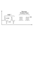
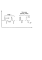
- FIGS. 14 to 16 are diagrams showing the polarity of the recovery pulse in the recovery operation after cycle driving for the FeFET according to one embodiment of the present invention.
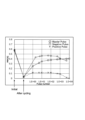
- FIGS. 17 to 19 are diagrams showing the polarity dependence, voltage dependence, and pulse width dependence of the recovery pulse for the MW after the recovery operation of the FeFET according to one embodiment of the present invention. Note that FIGS. 14 to 19 show the application method of the pulse voltage and the evaluation results for the memory device 10 in which the film thickness of the ferroelectric layer 220 is 5.2 nm.
- the pulse voltage in the recovery operation is called a "recovery pulse.”
- FIG. 14 shows a method of applying a "positive pulse voltage” as a recovery operation.
- the recovery operation is performed after cycle 1.
- Cycle 1 in FIG. 14 is the same as cycle 1 in FIG. 11.
- the thickness of the ferroelectric layer 220 of the memory device 10 described in FIG. 14 to FIG. 19 is 5.2 nm
- the positive pulse voltage in cycle 1 is 2.5 V
- the negative pulse voltage is -1.5 V.
- the positive pulse voltage in the recovery operation is 3 V
- the pulse width is 1 ⁇ sec.
- the pulse waveform is approximately rectangular.
- FIG. 15 shows a method of applying a "negative pulse voltage (Negative Pulse)" as a recovery operation.
- a negative pulse voltage Negative Pulse
- FIG. 15 shows a method of applying a "negative pulse voltage (Negative Pulse)" as a recovery operation.
- the negative pulse voltage in the recovery operation is -2V, and the pulse width is 1 ⁇ sec.
- the pulse waveform is approximately rectangular.
- FIG. 16 shows a method of applying a "bipolar pulse voltage" as a recovery operation.
- a positive pulse voltage and a negative pulse voltage are applied alternately to the ferroelectric layer 220.
- the application method shown in FIG. 16 is the same as the application method shown in FIG. 14.
- the positive pulse voltage in the recovery operation is 3V
- the negative pulse voltage is -2V
- the pulse width is 1 ⁇ sec.
- the pulse waveform is approximately rectangular.
- Figure 17 shows the results of evaluating the pulse voltage (recovery pulse) in the recovery operation shown in Figures 14 to 16.
- Figure 17 shows the MW after a recovery operation is performed with a specific number of pulses after cycle driving.
- the leftmost plot shows the MW before the start of cycle driving (Initial)
- the second plot from the left shows the MW after cycle driving (After cycling).
- the third and subsequent plots from the left show the MW measured after applying a predetermined number of pulse voltages.
- “ ⁇ ” shows the evaluation result when a bipolar pulse voltage is applied.
- ⁇ shows the evaluation result when a negative pulse voltage is applied.
- "X” shows the evaluation result when a positive pulse voltage is applied.
- the largest MW was obtained under the condition of applying a bipolar pulse voltage in the recovery operation.
- the smallest MW was obtained under the condition of applying a positive pulse voltage.
- the narrowed MW can be efficiently recovered.
- a remarkable MW recovery effect was obtained with only 2 pulses (2.E+0).
- a maximum MW recovery effect of about 0.1 V was obtained when applying a pulse voltage from 0 to 10 4 times. In other words, a good MW can be obtained by applying a bipolar pulse voltage in the recovery operation.
- Figure 18 shows the results of evaluating the voltage dependency for positive and negative pulse voltages in a method of applying a bipolar pulse voltage in the recovery operation.
- the [positive pulse voltage/negative pulse voltage] in the recovery operation is [2.7V/-1.7V], [3V/-2V], and [3.3V/-2.3V].
- the pulse width is 1 ⁇ sec.
- “ ⁇ ” indicates the evaluation result when [3.3V/-2.3V] is applied as the pulse voltage in the recovery operation.
- “ ⁇ ” indicates the evaluation result when [3V/-2V] is applied as the pulse voltage.
- “X” indicates the evaluation result when [2.7V/-1.7V] is applied as the pulse voltage.
- the MW after recovery operation under the conditions of [3V/-2V] and [3.3V/-2.3V] was larger than the MW after recovery operation under the condition of [2.7V/-1.7V].
- a good MW can be obtained by applying a voltage of 3V or more as the positive pulse voltage and a voltage of -2V or less as the negative pulse voltage during recovery operation.
- the above positive pulse voltage may be referred to as the "first pulse voltage” and the negative pulse voltage may be referred to as the "second pulse voltage.”
- the voltage applied by the first pulse voltage may be referred to as the "first voltage” and the voltage applied by the second pulse voltage may be referred to as the "second voltage.”
- the pulse voltage conditions for obtaining a good MW after the recovery operation as described above can be expressed as follows: The first voltage is positive, and the absolute value of the first voltage is 3.0 V or more. The second voltage is negative, and the absolute value of the second voltage is 2.0 V or more.
- the absolute values of the first voltage and the second voltage are 8.0 V or less.
- the positive pulse voltage is 3.0 V or more and 8.0 V or less.
- the negative pulse voltage is -8.0 V or more and -2.0 V or less.
- Figure 19 shows the results of evaluating pulse width dependency in a method of applying a bipolar pulse voltage in a recovery operation.
- the [positive pulse voltage/negative pulse voltage] in the recovery operation is [2.7V/-1.7V]
- the pulse widths of each pulse voltage are 1 ⁇ sec, 10 ⁇ sec, 100 ⁇ sec, and 1 msec.
- “ ⁇ ” indicates the evaluation result when the pulse width is 1 msec.
- “ ⁇ ” indicates the evaluation result when the pulse width is 100 ⁇ sec.
- “ ⁇ ” indicates the evaluation result when the pulse width is 10 ⁇ sec.
- “ ⁇ ” indicates the evaluation result when the pulse width is 1 ⁇ sec.
- the MW after the recovery operation tends to be larger as the pulse width becomes larger, but when the pulse width is in the range of 1 ⁇ sec to 1 msec, the change in MW with respect to the pulse width is not large, and good MW can be obtained under all conditions.
- the minimum pulse width in FIG. 19 is 1 ⁇ sec, but in this embodiment, the pulse width at which the recovery operation is effective is 0.1 ⁇ sec or more. Note that the pulse width may be 0.2 ⁇ sec or more, 0.3 ⁇ sec or more, or 0.5 ⁇ sec or more.
- the effect of recovering fatigue of the ferroelectric layer 220 by the recovery operation is affected by the total time of the pulse voltage applied to the ferroelectric layer 220. Therefore, for example, if the number of times the positive pulse voltage is applied is m (m is an integer of 1 or more), the number of times the negative pulse voltage is applied is n (n is an integer of 1 or more), the pulse width of the positive pulse voltage is a ⁇ sec, and the pulse width of the negative pulse voltage is b ⁇ sec, the conditions suitable for the recovery operation can be expressed as "Formula 1" and "Formula 2". 0.1 ⁇ sec ⁇ a ⁇ m ⁇ 250 ⁇ sec (Formula 1) 0.1 ⁇ sec ⁇ b ⁇ n ⁇ 250 ⁇ sec (Formula 2)
- the fatigue recovery of the ferroelectric layer 220 is insufficient, and the MW does not recover sufficiently. If the value of a ⁇ m is equal to or greater than the upper limit of formula 1 and the value of b ⁇ n is equal to or greater than the upper limit of formula 2, the time required for the recovery operation in the memory system 20 described below will be long, causing discomfort to the user.
- the film thickness of the ferroelectric layer 220 is made greater than 3 nm and smaller than 7 nm, low-voltage cyclic operation is possible, and a memory device 10 with high endurance characteristics can be realized. Furthermore, even if the MW is narrowed by low-voltage cyclic operation, a bipolar pulse voltage is applied as the pulse voltage in the recovery operation, and the positive pulse voltage in the bipolar pulse voltage is 3 V or more, the negative pulse voltage is -2 V or less, and the pulse width of these pulse voltages is 0.1 ⁇ sec or more, so that the narrowed MW can be restored (enlarged), and a memory device 10 with high endurance characteristics can be realized even after the recovery operation.
- Fig. 20 is a schematic diagram of a memory cell array according to one embodiment of the present invention.
- a memory chip 300 includes a memory cell array 310 and a peripheral circuit 320.
- the peripheral circuit 320 is provided on the periphery of the memory cell array 310.
- the peripheral circuit 320 is provided in the X direction and the Y direction of the memory cell array 310.
- Memory cell array 310 comprises multiple memory blocks MB0 to MBj (j is a natural number) arranged in the Y direction. Each of memory blocks MB0 to MBj comprises multiple pages. In each page, memory cells equipped with the above-mentioned memory device 10 are arranged in a matrix. A page is a unit for executing data read operations and program operations. On the other hand, memory block MBi (i is an integer between 0 and j) is a unit for executing data erase operations.
- the peripheral circuit 320 generates a voltage in response to a command received from the outside and applies the generated voltage to the memory cell array 310 to perform a program operation, read operation, or erase operation on the page or memory block specified by the command.
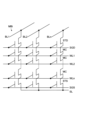
- FIG. 21 is a circuit diagram of a memory cell array according to one embodiment of the present invention.
- the circuit diagram shown in FIG. 21 is an equivalent circuit diagram showing the configuration of one memory block MBi.
- Memory block MBi includes memory cells MC, select transistors STD, STS, bit lines BL (BL1 to BLm), source lines SL, word lines WL (WL1 to WLn), and select gate lines SGD, SGS.
- the memory device 10 described in the first embodiment is used as the memory cells MC. Note that m and n are natural numbers equal to or greater than 2.
- Memory cells MC and select transistors STD, STS are directly connected between the bit line BL and the source line SL. In this way, multiple memory cells MC directly connected between the bit line BL and the source line SL are sometimes called a memory string.
- the peripheral circuit 320 controls the voltages supplied to the bit lines BL, source lines SL, word lines WL, and select gate lines SGD and SGS to perform a program operation, read operation, or erase operation on the page or memory block specified by the command.
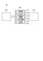
- Fig. 22 is a schematic diagram of a memory system according to an embodiment of the present invention. As shown in Fig. 22, the memory system 20 includes a memory chip 300 and a memory controller 400. The memory controller 400 communicates with a host 500 and controls the memory chip 300 based on an instruction from the host 500.
- the memory controller 400 includes a logical-physical conversion table 410, an MPU 420, an operation count storage unit 430, an ECC circuit 440, and an error rate storage unit 450.
- the logical-physical conversion table 410 stores a logical address included in an instruction received from the host 500 in association with a physical address assigned to each page of the memory cell array 310.
- the operation count storage unit 430 stores a physical address corresponding to a memory block MBi or a page in association with the number of program operations, read operations, or erase operations performed on the memory block MBi or the page.
- the ECC circuit 440 detects errors in the data read from the memory chip 300, and corrects the data if there is an error in the data.
- the error rate storage unit 450 stores a physical address corresponding to the memory block MBi or the page in association with a bit error rate corresponding to the memory block MBi or the page.
- the bit error rate may be the average value of the bit error rates calculated for each page, or may be the maximum value.
- the MPU 420 controls the memory chip 300 in cooperation with the logical-physical conversion table 410, the operation count storage unit 430, the ECC circuit 440, and the error rate storage unit 450.
- the memory controller 400 or the MPU 420 may be referred to as a control circuit. In this case, it can be said that the control circuit controls the memory cell array 310.
- FIG. 23 is a flowchart showing a recovery operation of a memory system according to an embodiment of the present invention. Each step in the flowchart shown in Fig. 23 is executed by the logical-physical conversion table 410, the MPU 420, the operation count storage unit 430, the ECC circuit 440, and the error rate storage unit 450 of the memory controller 400 working together.
- the MPU 420 acquires a physical address corresponding to the memory block MBi or page that is programmable or to be erased based on the logical address specified by the command (step S1102; acquire physical address).
- the MPU 420 transmits the acquired physical address and the program command or erase command to the memory chip 300 and executes a program operation or erase operation (step S1103; program/erase command).
- the MPU 420 refers to the operation count storage unit 430 and updates the program count or erase count of the memory block MBi or page that corresponds to the physical address where the above operation was executed (step S1104; update program/erase count).
- the MPU 420 refers to the updated operation count storage unit 430 and determines whether the number of times program operations or erase operations have been performed on the updated memory block MBi or page (or memory cells contained therein) has reached a predetermined number (threshold) (step S1105; ⁇ threshold?). If it is determined in S1105 that the number of executions has reached the threshold ("Yes" in S1105), the MPU 420 causes the memory chip 300 to perform the recovery operation described in the first embodiment (step S1106; Execute recovery operation). On the other hand, if the number of executions is less than the threshold in S1105 ("No" in S1105), the MPU 420 ends the flowchart of FIG. 23.
- the recovery operation is a voltage supply operation in which a first voltage of a first polarity and a second voltage of a second polarity opposite to the first polarity are applied to the ferroelectric layer 220.
- the first polarity is positive, and the first voltage is a positive pulse voltage.
- a pulse voltage of 3 V is supplied, which is greater than the maximum voltage (2.5 V) in the program operation.
- the second polarity is negative, and the second voltage is a negative pulse voltage.
- a pulse voltage of -2 V is supplied, which is greater than the maximum voltage (-1.5 V) in the erase operation.
- the magnitude relationship between the voltages in the above positive and negative polarities refers to the magnitude relationship between the absolute values of the voltages in each operation.
- a negative voltage e.g., -2.5V
- a positive voltage e.g., 1.5V
- the first polarity is negative
- the first voltage is a negative pulse voltage
- a -3V pulse voltage is supplied as the first voltage of the first polarity
- a 2V pulse voltage is supplied as the second voltage of the second polarity.
- FIG. 24 is a flowchart showing the recovery operation of a memory system according to one embodiment of the present invention. Each step in the flowchart shown in FIG. 24 is executed by the logical-physical conversion table 410, MPU 420, operation count storage unit 430, ECC circuit 440, and error rate storage unit 450 of the memory controller 400 working together, similar to each step in FIG. 23.
- Steps S1201 to S1203 in the flowchart of FIG. 24 are the same as S1101 to S1103 in FIG. 23, so a description thereof will be omitted.
- the MPU 420 transmits data received from the memory chip 300 to the ECC circuit 440 and acquires the bit error rate of this data (step S1200; read; acquire bit error rate).
- the ECC circuit 440 associates the acquired bit error rate with an appropriate physical address and stores it in the error rate storage unit 450.
- the MPU 420 After S1203, the MPU 420, after executing the program operation or erase operation, refers to the error rate storage unit 450 and determines whether the bit error rate of the memory block MBi or page on which the program operation or erase operation was executed has reached a predetermined probability (threshold) (step S1204; ⁇ threshold?). If it is determined in S1204 that the bit error rate has reached the threshold ("Yes" in S1204), the MPU 420 causes the memory chip 300 to execute the recovery operation described in the first embodiment (step S1205; execute recovery operation). On the other hand, if the bit error rate is less than the threshold in S1204 ("No" in S1204), the MPU 420 ends the flowchart of FIG. 24.
- threshold a predetermined probability
- a memory device 30 in which a ferroelectric layer is used as a layer having a memory function, as in the first embodiment, is exemplified.
- the memory device 30 is an FeFET in which an oxide semiconductor layer is used as a layer functioning as a channel.
- FIG. 36 is a schematic cross-sectional view showing an FeFET according to one embodiment of the present invention.
- the memory device 30 includes a substrate 110, a gate electrode 120, a ferroelectric layer 130, a channel layer 140, a protective insulating layer 150, a source electrode 170, and a drain electrode 180.
- the gate electrode 120 is provided on the substrate 110.
- the channel layer 140 is provided in a position facing the gate electrode 120.
- the ferroelectric layer 130 is provided between the gate electrode 120 and the channel layer 140.
- the protective insulating layer 150 is provided on the channel layer 140 so as to cover the pattern end of the channel layer 140.
- the protective insulating layer 150 has an opening reaching the channel layer 140.
- the source electrode 170 and the drain electrode 180 are provided in the opening.
- a semiconductor substrate or an insulating substrate is used.
- the semiconductor substrate for example, a silicon substrate or an SOI substrate is used.
- the insulating substrate for example, a glass substrate or a quartz substrate is used.
- the gate electrode 120, the source electrode 170, and the drain electrode 180 general metal materials are used.
- materials such as molybdenum, tungsten, titanium, and aluminum are used.
- HZO for example, can be used as the ferroelectric layer 130.
- a layer containing at least any of silicon, magnesium, aluminum, barium, zirconium, gadolinium, lanthanum, samarium, nitrogen, and yttrium may be used as the ferroelectric layer 130.
- a barrier layer that prevents the diffusion of the impurities may be provided between the substrate 110 and the ferroelectric layer 130. Silicon nitride, for example, may be used as the barrier layer.
- An oxide semiconductor is used as the channel layer 140.
- an oxide semiconductor containing indium, gallium, and zinc (IGZO), an oxide semiconductor containing indium, tin, and zinc (ITZO), an oxide semiconductor containing indium and zinc (IZO), an oxide semiconductor containing indium and tin (ITO), or indium oxide is used.
- a general insulating material is used as the protective insulating layer 150.
- an inorganic insulating layer such as silicon oxide, silicon nitride, aluminum oxide, or aluminum nitride is used as the protective insulating layer 150.
- An organic insulating layer such as a polyimide substrate, an acrylic substrate, a siloxane substrate, or a fluororesin substrate may also be used as the protective insulating layer 150.
- the protective insulating layer 150 may have a structure in which the above materials are laminated.
- the thickness of the ferroelectric layer 130 can be made greater than 1 nm and smaller than 30 nm. If the thickness of the ferroelectric layer 130 is within the above range, low-voltage driving similar to the low-voltage driving of the memory device 10 of the first embodiment can be performed. As a result, even if the MW is narrowed by cyclic driving of the memory device 30, the MW can be restored by the recovery operation described in the first embodiment. In addition, in order to ensure the polarization characteristics (ferroelectric characteristics) of the ferroelectric layer 130, the thickness of the ferroelectric layer 130 may be made greater than 3 nm.
- the thickness of the ferroelectric layer 130 is 4.6 nm or more and 6 nm or less.
- FIG. 37 is a perspective view showing the configuration of a memory cell according to one embodiment of the present invention.
- the memory cell MC has a conductive layer 610, a semiconductor layer 620, an oxide insulating layer 630, and a ferroelectric layer 640.
- the conductive layer 610 is formed along the main surface of the substrate. That is, the conductive layer 610 extends in the XY plane.
- the conductive layers 610 are stacked in the Z direction. Two conductive layers 610 adjacent in the Z direction are separated by an insulating layer (not shown). That is, the conductive layers 610 and insulating layers are stacked alternately on the substrate.
- the semiconductor layer 620 is provided inside a memory hole that penetrates the stacked conductive layer 610 and insulating layer.
- the semiconductor layer 620 is columnar or cylindrical. In FIG. 37, a cylindrical configuration of the semiconductor layer 620 is illustrated, but the semiconductor layer 620 may be polygonal columnar or truncated cone. When the semiconductor layer 620 is cylindrical, the hollow part of the cylindrical shape is filled with a filler such as silicon oxide.
- the oxide insulating layer 630 is provided around the semiconductor layer 620.
- the ferroelectric layer 640 is provided around the oxide insulating layer 630. The oxide insulating layer 630 is in contact with the semiconductor layer 620, and the ferroelectric layer 640 is in contact with the oxide insulating layer 630 and the conductive layer 610.
- Another layer may be provided between the semiconductor layer 620 and the oxide insulating layer 630.
- Another layer may be provided between the oxide insulating layer 630 and the ferroelectric layer 640.
- Other layers may be provided between the ferroelectric layer 640 and the conductive layer 610.
- the semiconductor layer 620 functions as a channel.
- the conductive layer 610 functions as a gate electrode.
- the oxide insulating layer 630 and the ferroelectric layer 640 function as gate insulating layers.
- a voltage is applied to the conductive layer 610, an electric field is formed in the semiconductor layer 620 via the oxide insulating layer 630 and the ferroelectric layer 640, and carriers are generated in the semiconductor layer 620 by this electric field.
- the memory cell MC is a vertical FeFET that passes a current in the vertical direction (Z direction).
- the conductive layer 610 corresponds to the gate electrode 230.
- the semiconductor layer 620 corresponds to the semiconductor layer 200.
- the oxide insulating layer 630 corresponds to the oxide insulating layer 210.
- the ferroelectric layer 640 corresponds to the ferroelectric layer 220. Therefore, the memory cell MC operates in the same manner as the memory device 10.
- a plurality of the memory cells MC are provided in the Z direction along the pillar-shaped semiconductor layer 620. In other words, a plurality of memory cells MC are connected in series along the semiconductor layer 620.
- HZO-based FeFETs have been recognized as promising candidates for non-volatile memory, logic, and AI accelerators.
- various challenges including high voltage operation and low endurance (typically ⁇ 10 5 ) have been a major impediment to their application.
- Scaling of HZO film thickness has been proven to be an effective approach to lower voltage and improve endurance in MFM capacitors in FeRAMs.
- fatigue degradation in MFM capacitors can be recovered and endurance can be improved.
- systematic studies of the effects of HZO film thickness scaling on device characteristics and MW narrowing in FeFETs remain lacking.
- [Device Fabrication] 25 shows the process flow and TEM images of the TiN/HZO/ SiO2FeFET employed in this study.
- the ALD HZO film thicknesses are 11 nm, 8 nm, 6 nm, and 4.6 nm.
- the RTA temperature was set at 450°C to obtain optimal interface conditions and ferroelectric properties in the thin HZO film.
- FIG. 26A shows the setup for P-V measurements on FeFETs.
- Results in FIGS. 26B-E show that the thinner films provide lower Vc , which is advantageous for low voltage operation, as evidenced by the higher 2Pr in the same voltage range.
- Id - Vg characteristics (FIGS. 27A-D) and extracted MW (FIG. 28) show that even in the low Vg range of -0.5V/2V, the 6nm and 4.6nm FeFETs have larger MW at 0.7V and 0.8V than the MW at 0.3V and 0.05V for the 11nm and 8nm FeFETs.
- FIGS. 29A-D show MW mappings determined from Vth and fast Id - Vg characteristics under 1 ⁇ s program/erase pulse conditions, revealing that the thin film HZO FeFETs operate at lower voltages.
- Figure 30(a) compares the Id - Vg curves of FeFETs with four different HZO thicknesses at MW of 0.8 V.
- the erase/program pulse voltage is reduced from -2.4 V/3.2 V (11 nm) to -1.6 V/2.7 V (4.6 nm).
- the thin HZO FeFETs exhibit a higher Ion / Ioff ratio at the same MW, which is 9.5 times that of the 4.6 nm HZO FeFET at 11 nm.
- Figure 31 shows the endurance characteristics of FeFETs with different HZO thicknesses at (a) the same electric field and (b) the same memory window at 0.5 V.
- the 6-nm and 4.6-nm HZO FeFETs show approximately twice the endurance ( ⁇ 105 ) compared to the 11-nm one ( 5x10⁴ ).
- the endurance of the 6-nm and 4.6-nm HZO FeFETs is also larger than that of the 11-nm device, reaching 1x10⁶ .
- [Improve endurance by recovering fatigue] 33A-33D show the endurance characteristics of FeFETs after repeated recovery pulses, together with the initial MW.
- the 6 nm and 4.6 nm HZO FeFETs recover well after the first and second recovery pulses, with endurance of 106 cycles in the second and third cycles.
- the 11 nm and 8 nm HZO FeFETs recover weakly, with MW below 0.25 V after recovery and far fewer cycles than 106. This difference is due to the degradation of the MOS interface in the thick HZO FeFET (FIGS. 34A-34D).
- the S value and MW are significantly degraded in the thick HZO FeFET.
- the electric field in the HZO is estimated to be smaller for the thicker HZO FeFET with a fixed MW, and the severe degradation in the thick FeFET is due to the high voltage operation. With an improved interface, higher endurance can be expected by applying the above method to FeFETs.
- the ferroelectric memory device has a thickness of the ferroelectric layer greater than 3 nm and smaller than 7 nm.
- ferroelectric layer contains at least one of silicon, magnesium, aluminum, barium, zirconium, gadolinium, lanthanum, samarium, nitrogen, and yttrium in addition to hafnium and oxygen.
- a control circuit for controlling the memory cells includes: determining whether a program operation or an erase operation has been performed on the memory cell a predetermined number of times; when it is determined that the number of executions has reached the predetermined number, a voltage supply operation is performed to apply a first voltage of a first polarity and a second voltage of a second polarity opposite to the first polarity to the ferroelectric layer; the first voltage is greater than a maximum voltage in the program operation; The second voltage is greater than a maximum voltage in the erase operation.
- a control circuit for controlling the plurality of memory cells includes: determining whether the bit error rate is equal to or greater than a predetermined probability; when it is determined that the bit error rate is equal to or greater than the predetermined probability, a voltage supply operation is performed to apply a first voltage of a first polarity and a second voltage of a second polarity opposite to the first polarity to the ferroelectric layer; the first voltage is greater than a maximum voltage in the program operation; The second voltage is greater than a maximum voltage in the erase operation.
- the ferroelectric layer of the ferroelectric memory device has a thickness greater than 1 nm and smaller than 30 nm.
- ferroelectric layer contains at least one of silicon, magnesium, aluminum, barium, zirconium, gadolinium, lanthanum, samarium, nitrogen, and yttrium in addition to hafnium and oxygen.
- a control circuit for controlling the memory cells includes: determining whether a program operation or an erase operation has been performed on the memory cell a predetermined number of times; when it is determined that the number of executions has reached the predetermined number, a voltage supply operation is performed to apply a first voltage of a first polarity and a second voltage of a second polarity opposite to the first polarity to the ferroelectric layer; the first voltage is greater than a maximum voltage in the program operation; The second voltage is greater than a maximum voltage in the erase operation.
- a control circuit for controlling the plurality of memory cells includes: determining whether the bit error rate is equal to or greater than a predetermined probability; when it is determined that the bit error rate is equal to or greater than the predetermined probability, a voltage supply operation is performed to apply a first voltage of a first polarity and a second voltage of a second polarity opposite to the first polarity to the ferroelectric layer; the first voltage is greater than a maximum voltage in the program operation; The second voltage is greater than a maximum voltage in the erase operation.
Landscapes
- Engineering & Computer Science (AREA)
- Computer Hardware Design (AREA)
- Semiconductor Memories (AREA)
- Thin Film Transistor (AREA)
- Non-Volatile Memory (AREA)
Abstract
記憶装置は、半導体層と、前記半導体層と対向するゲート電極と、前記半導体層と前記ゲート電極との間に設けられた絶縁層と、前記絶縁層と前記ゲート電極との間に設けられ、酸化ハフニウムを含む強誘電体層と、を備え、前記強誘電体層の膜厚は、3nmより大きく7nmより小さい、又は、酸化物半導体層と、前記酸化物半導体層と対向するゲート電極と、前記酸化物半導体層と前記ゲート電極との間に設けられ、酸化ハフニウムを含む強誘電体層と、を備え、前記強誘電体層の膜厚は、3nmより大きく30nmより小さい。
Description
本発明の一実施形態は、記憶装置及びメモリシステムに関する。特に、本発明の一実施形態は、強誘電体層を備えた記憶装置及び当該記憶装置を備えたメモリシステムに関する。
近年、強誘電体層を備えた記憶装置の開発が進められている。このような記憶装置として、トランジスタ(MOS FET)のゲート絶縁層に酸化ハフニウムが用いられたメモリセルの開発が進められている。このようなトランジスタ型のメモリセルはFeFET(Ferroelectric FET)と呼ばれている。FeFETは、不揮発性でありながら、高速プログラム及び消去が可能であり、かつ低消費電力で駆動可能な記憶装置として期待されている(例えば、特許文献1及び非特許文献1~3)。なお、非特許文献1~3は、本願においてパリ条約による優先権を主張する米国仮出願63/506675の出願後に公開された文献である。
Bong Ho Kim, Seong Kwang Kim, Song-hyeon Kuk, Yoon-Je Suh, Jaeyong Jeong, Joon Pyo Kim, Dae-Myeong Geum, and Sanghyeon Kim, "IL Scavenging and Recovery Strategies to Improve the Performance and Reliability of HZO-Based FeFETs," IEEE International Electron Devices Meeting (IEDM), 18-3, 2023.
C.-H. Wu, J. Liu, X.-T. Zheng, Y.-M. Tseng, M. Kobayashi, V. P.-H. Hu, and C.-J. Su, "Robust Recovery Scheme for MFIS-FeFETs at Optimal Timing with Prolonged Endurance: Fast-Unipolar Pulsing (100 ns), Nearly Zero Memory Window Loss (0.02 %), and Self-Tracking Circuit Design," IEEE International Electron Devices Meeting (IEDM), 18-2, 2023.
C.-H. Wu, J. Liu, X.-T. Zheng, H.-F. Chuang, Y.-M. Tseng, M. Kobayashi, C.-J. Su, and V. P.-H. Hu, "Innovative Recovery Strategy for MFIS-FeFETs at Optimal Timing With Robust Endurance: Fast-Unipolar Pulsing (100 ns), Nearly Zero Memory Window Loss (0.02%), and Self-Tracking Circuit Design," IEEE Transactions on Electron Devices, 2024.
FeFETでは、メモリセルに対してデータをプログラムする際のプログラム電圧及びメモリセルのデータを消去する際の消去電圧の影響によって、FeFETを構成する積層薄膜間の界面(例えば、シリコン基板上の酸化シリコンと強誘電体層との間の界面)が劣化し、その結果、書き換え耐性(エンデュランス特性)が悪化する、という問題が起きる場合がある。
本発明の課題の一つは、エンデュランス特性が高い記憶装置を提供することである。
本発明の一実施形態における記憶装置は、半導体層と、前記半導体層と対向するゲート電極と、前記半導体層と前記ゲート電極との間に設けられた絶縁層と、前記絶縁層と前記ゲート電極との間に設けられ、酸化ハフニウムを含む強誘電体層と、を備え、前記強誘電体層の膜厚は、3nmより大きく7nmより小さい。
本発明の一実施形態における記憶装置は、酸化物半導体層と、前記酸化物半導体層と対向するゲート電極と、前記酸化物半導体層と前記ゲート電極との間に設けられ、酸化ハフニウムを含む強誘電体層と、を備え、前記強誘電体層の膜厚は、1nmより大きく30nmより小さい。
本発明の一実施形態におけるメモリシステムは、記憶装置を備えたメモリセルがマトリクス状に配置されたメモリセルアレイと、前記メモリセルアレイを制御する制御回路と、を備え、前記制御回路は、前記メモリセルに対するプログラム動作又は消去動作の実行回数が所定数に達したか否かを判定し、前記実行回数が前記所定数に達したと判定した場合、第1極性の第1電圧と、前記第1極性とは逆の第2極性の第2電圧と、を前記強誘電体層に印加する電圧供給動作を実行し、前記第1電圧は、前記プログラム動作における最大電圧より大きく、前記第2電圧は、前記消去動作における最大電圧より大きい。
本発明の一実施形態におけるメモリシステムは、記憶装置がマトリクス状に配置された複数のメモリセルアレイと、前記複数のメモリセルアレイを制御する制御回路と、を備え、前記制御回路は、プログラム動作又は消去動作を実行した後にビットエラー率が所定確率以上か否かを判定し、前記ビットエラー率が前記所定確率以上であると判定した場合、第1極性の第1電圧と、前記第1極性とは逆の第2極性の第2電圧と、を前記強誘電体層に印加する電圧供給動作を実行し、前記第1電圧は、前記プログラム動作における最大電圧より大きく、前記第2電圧は、前記消去動作における最大電圧より大きい。
以下、本発明の実施形態について、図面等を参照しつつ説明する。但し、本発明は、その要旨を逸脱しない範囲において様々な態様で実施することができる。本発明は、以下に例示する実施形態の記載内容に限定して解釈されない。図面は、説明をより明確にするため、実際の態様に比べ、各部の幅、膜厚、形状等について模式的に表される場合がある。しかしながら、図面は、あくまで一例であって、本発明の解釈を限定するものではない。
本発明の実施形態を説明する場合、基板からゲート電極に向かう方向を「上」と表現し、その逆の方向を「下」と表現する。ただし、「上に」又は「下に」という表現は、単に、各要素の上下関係を説明しているにすぎない。例えば、基板の上にゲート電極が配置されるという表現は、基板とゲート電極との間に他の部材が介在する場合も含む。さらに、「上に」又は「下に」という表現は、平面視において各要素が重畳する場合だけでなく、重畳しない場合を含む。「直上」又は「直下」という表現は、平面視において各要素が重畳する場合を指す。
本明細書において「αはA、B又はCを含む」、「αはA、B及びCのいずれかを含む」、「αはA、B及びCからなる群から選択される一つを含む」といった表現は、特に明示が無い限り、αはA~Cの複数の組み合わせを含む場合を排除しない。さらに、これらの表現は、αが他の要素を含む場合も排除しない。
[1.第1実施形態]
図1~図19を用いて、本発明の一実施形態に係る記憶装置10の構成について説明する。以下の実施形態では、メモリ機能を備える層として強誘電体層220が用いられた記憶装置10が例示されている。記憶装置10は、強誘電体層220がゲート絶縁層として用いられたMOSFETであり、「FeFET」と呼ばれている。
図1~図19を用いて、本発明の一実施形態に係る記憶装置10の構成について説明する。以下の実施形態では、メモリ機能を備える層として強誘電体層220が用いられた記憶装置10が例示されている。記憶装置10は、強誘電体層220がゲート絶縁層として用いられたMOSFETであり、「FeFET」と呼ばれている。
[1-1.記憶装置10の構成]
図1は、本発明の一実施形態に係るFeFETを示す概略断面図である。図1に示すように、記憶装置10は、半導体層200、酸化物絶縁層210、強誘電体層220、ゲート電極230、及び電極250を有する。半導体層200は、半導体基板の一部(上層部分)であってもよく、例えばSOI(Silicon on Insulator)のように絶縁層基板の上に形成された半導体層であってもよい。酸化物絶縁層210は、半導体層200の上に設けられている。強誘電体層220は、酸化物絶縁層210の上に設けられている。酸化物絶縁層210及び強誘電体層220を併せてゲート絶縁層という場合がある。ゲート電極230は、強誘電体層220の上に設けられている。ゲート電極230は、第1導電層231及び第2導電層232を含む。なお、本実施形態では、ゲート電極230は2層構造であるが、ゲート電極230は1層構造であってもよく、3層以上の構造であってもよい。
図1は、本発明の一実施形態に係るFeFETを示す概略断面図である。図1に示すように、記憶装置10は、半導体層200、酸化物絶縁層210、強誘電体層220、ゲート電極230、及び電極250を有する。半導体層200は、半導体基板の一部(上層部分)であってもよく、例えばSOI(Silicon on Insulator)のように絶縁層基板の上に形成された半導体層であってもよい。酸化物絶縁層210は、半導体層200の上に設けられている。強誘電体層220は、酸化物絶縁層210の上に設けられている。酸化物絶縁層210及び強誘電体層220を併せてゲート絶縁層という場合がある。ゲート電極230は、強誘電体層220の上に設けられている。ゲート電極230は、第1導電層231及び第2導電層232を含む。なお、本実施形態では、ゲート電極230は2層構造であるが、ゲート電極230は1層構造であってもよく、3層以上の構造であってもよい。
上記の構成を換言すると、以下のように表現することができる。ゲート電極230は半導体層200と対向する。酸化物絶縁層210は、半導体層200とゲート電極230との間に設けられている。強誘電体層220は、酸化物絶縁層210とゲート電極230との間に設けられている。なお、酸化物絶縁層210は界面層(an interface layer)ともいい、半導体層200はチャネル層(a channel layer)ともいう。
半導体層200には、低抵抗領域201及びチャネル領域202が設けられている。低抵抗領域201は、平面視でゲート電極230とは重ならない領域である。低抵抗領域201の半導体層200には、半導体層200の抵抗を下げる不純物が導入されている。例えば、半導体層200がシリコンを含む場合、記憶装置10がN型のMOSFETであれば、当該不純物としてリン(P)が用いられ、記憶装置10がP型のMOSFETであれば、ボロン(B)が用いられる。チャネル領域202は、離隔された2つの低抵抗領域201に挟まれた領域である。2つの低抵抗領域201のうち、一方はソース領域として機能し、他方はドレイン領域として機能する。チャネル領域202の半導体層200は、ゲート電極230に供給される電圧によってオン状態とオフ状態とが切り替えられる性質を備えている。
酸化物絶縁層210は、チャネル領域202の半導体層200と接する。酸化物絶縁層210の膜厚は、5nm未満、3nm以下、2nm以下、1nm以下、又は0.7nm以下である。いずれの場合においても、酸化物絶縁層210の膜厚は0nmより大きい。酸化物絶縁層210は、例えば、半導体層200が酸化された層である。半導体層200がシリコン基板である場合、酸化物絶縁層210は酸化シリコンを含む。例えば、酸化物絶縁層210は、塩酸水、過酸化水素水、及び水の混合溶液を半導体層200に塗布する、又は当該混合溶液に半導体層200を浸漬させることで得られる。より具体的には、酸化物絶縁層210は、RCA洗浄に含まれるSC2(Standard Clean 2)処理によって形成される。ただし、酸化物絶縁層210は、半導体層200に対する熱酸化によって形成されてもよい。
強誘電体層220は、外部から電界が印加されていない状態であっても電気双極子が整列している誘電体層である。強誘電体層220は、外部から電界が印加されることによって、電気双極子の向きが変化する誘電体層である。このような強誘電体層220がゲート絶縁層として用いられることで、強誘電体層220の電気双極子の向きによって記憶装置10のId-Vg特性(Id:ドレイン電流、Vg:ゲート電圧)における閾値電圧がシフトする。このような特性を利用して、記憶装置10はメモリセルとして利用される。本実施形態では、強誘電体層220として、酸化ハフニウムを含む強誘電体が用いられる。例えば、強誘電体層220として、酸化ハフニウム及び酸化ジルコニウムの混晶(HZO;Hf0.5Zr0.5O2)が用いられる。強誘電体層220は酸化物絶縁層210と接する。強誘電体層220の膜厚は、3nmより大きく7nmより小さい又は4.6nm以上6nm以下である。
本実施形態では、強誘電体層220が酸化物絶縁層210と接する構成が例示されているが、強誘電体層220と酸化物絶縁層210との間に他の層が設けられていてもよい。強誘電体層220は、ハフニウム及び酸素に加えて、少なくともシリコン、マグネシウム、アルミニウム、バリウム、ジルコニウム、ガドリニウム、ランタン、サマリウム、窒素、及びイットリウムのいずれかを含んでもよい。
ゲート電極230は、記憶装置10のオン状態とオフ状態とを切り替えるための電圧(ゲート電圧)、又は強誘電体層220の電気双極子の向きを変化させるための電圧(プログラム電圧又は消去電圧)が供給される電極である。例えば、第1導電層231として窒化チタン、タングステン、窒化タングステン、ルテニウム、及び酸化ルテニウムを用いることができる。第2導電層232としてアルミニウム及び多結晶シリコンを用いることができる。
酸化物絶縁層210及び強誘電体層220には、コンタクトが設けられている。当該コンタクトは、半導体層200の低抵抗領域201に達する。当該コンタクトの内部に導電層が成膜されることによって、電極250が形成されている。2つの電極250のうち、ソース領域に接続される電極はソース電極であり、ドレイン領域に接続される電極はドレイン電極である。電極250として、一般的な金属材料が用いられる。例えば、電極250として、CVD(Chemical Vapor Deposition)法で成膜することが可能なタングステンが用いられる。
[1-2.記憶装置10の製造方法]
図2は、本発明の一実施形態に係るFeFETの製造方法を示すシーケンス図である。図2に示すように、まず、半導体層200を含む基板に対して基板クリーニングを行う(ステップS1001;基板クリーニング)。例えば、基板クリーニングとしてRCA洗浄を行う。RCA洗浄は、SC1処理(Standard Clean 1)及び上記のSC2処理を含む洗浄である。SC1処理は、水酸化アンモニウム水、過酸化水素水、及び水の混合溶液を半導体層200に塗布する、又は当該混合溶液に半導体層200を浸漬させる処理である。
図2は、本発明の一実施形態に係るFeFETの製造方法を示すシーケンス図である。図2に示すように、まず、半導体層200を含む基板に対して基板クリーニングを行う(ステップS1001;基板クリーニング)。例えば、基板クリーニングとしてRCA洗浄を行う。RCA洗浄は、SC1処理(Standard Clean 1)及び上記のSC2処理を含む洗浄である。SC1処理は、水酸化アンモニウム水、過酸化水素水、及び水の混合溶液を半導体層200に塗布する、又は当該混合溶液に半導体層200を浸漬させる処理である。
次に、フォトリソグラフィ工程によって、後のステップで低抵抗領域201になる領域が開口されたマスクを形成し、開口された領域の半導体層200に対して不純物のイオン注入を行う(ステップS1002;S/Dイオン注入)。次に、注入された不純物に対する熱活性化を行う(ステップS1003;熱活性化)。S1003における熱活性化は、例えば1000℃の熱処理によって行われる。
次に、半導体層200の表面にSC2処理を行う。このSC2処理によって、半導体層200の表面に酸化物絶縁層210を形成する(ステップS1004;酸化物絶縁層形成)。このような薬液による酸化(ケミカル酸化)によって酸化物絶縁層210が形成される場合、形成された酸化物絶縁層210の膜厚は非常に薄い。詳細は後述するが、本実施形態では、形成された酸化物絶縁層210の膜厚は約0.7nmである。
次に、酸化物絶縁層210の上に強誘電体層220を形成する(ステップS1005;強誘電体層形成)。強誘電体層220は、例えば原子層堆積法(ALD;Atomic Layer Deposition)によって形成される。ただし、強誘電体層220をその他の方法で形成してもよい。次に、強誘電体層220の上に第1導電層231及び第2導電層232(ゲート電極230)を形成する(ステップS1006;導電層形成)。S1006で形成された導電層に対してマスクを形成し、マスクを介して当該導電層に対してエッチングを行うことで、ゲート電極230のパターンを形成する(ステップS1007;ゲートパターニング)。S1007によって、ゲート電極230のパターンが形成された領域以外の強誘電体層220が露出される。
次に、S1007で露出された強誘電体層220及びその下の酸化物絶縁層210にコンタクトを開孔し(ステップS1008;コンタクト開孔)、コンタクトの内部に導電層を成膜することで、電極250を形成する(ステップS1009;S/D電極形成)。S1009で電極250が形成された後に、熱処理を行う(ステップS1010;熱処理)。当該熱処理は、例えば、400℃、30秒の条件で行われる。
なお、本実施形態では、酸化物絶縁層210を形成する前にS1002のイオン注入を行う製造方法が例示されているが、この製造方法に限定されない。例えば、S1007のゲートパターニングの後に、ゲートパターンをマスクとして半導体層200にイオン注入を行ってもよい。
[1-3.強誘電体層220の断面TEM像]
本実施形態において、図1に示す記憶装置10であって、強誘電体層220の膜厚が異なる記憶装置10を作製して、各種評価を行った。図3は、本発明の一実施形態に係るFeFETの強誘電体層の断面TEM像である。図3では4つの断面TEM像が示されている。図3において、左から強誘電体層220の膜厚が11nm、8nm、6nm、及び4.6nmである記憶装置10の断面TEM像である。図3に示す断面TEM像から、本実施形態において用いられた強誘電体層220の膜厚がほぼ上記の数値通りであること、及び強誘電体層220が良好な結晶性を示すことが確認される。なお、図3に示す断面TEM像から、酸化物絶縁層210の膜厚が約0.7nmであることが確認される。
本実施形態において、図1に示す記憶装置10であって、強誘電体層220の膜厚が異なる記憶装置10を作製して、各種評価を行った。図3は、本発明の一実施形態に係るFeFETの強誘電体層の断面TEM像である。図3では4つの断面TEM像が示されている。図3において、左から強誘電体層220の膜厚が11nm、8nm、6nm、及び4.6nmである記憶装置10の断面TEM像である。図3に示す断面TEM像から、本実施形態において用いられた強誘電体層220の膜厚がほぼ上記の数値通りであること、及び強誘電体層220が良好な結晶性を示すことが確認される。なお、図3に示す断面TEM像から、酸化物絶縁層210の膜厚が約0.7nmであることが確認される。
[1-4.記憶装置10のId-Vg特性]
図4は、本発明の一実施形態に係るFeFETのId-Vg特性を示す図である。図4に示す4つのグラフは、それぞれ強誘電体層220の膜厚が異なる4種類の記憶装置10に対して測定されたId-Vg特性である。Vgはゲート電極230に印加される電圧である。Idはソース電極として機能する電極250とドレイン電極として機能する電極250との間に流れる電流である。なお、ソース領域として機能する低抵抗領域201とドレイン領域として機能する低抵抗領域201と間の距離(チャネル長)は10μmであり、チャネル長に直交するチャネル幅は100μmである。Id-Vg特性測定時における電極250間のドレイン電圧は0.05Vである。図4に示すId-Vg特性は、ゲート電極230に電圧を印加し続けた状態でVgのスキャンを行っており、Vgに高電圧が印加されると強誘電体層220において分極反転が起きる。このようなId-Vg特性を「DC Id-Vg」という場合がある。
図4は、本発明の一実施形態に係るFeFETのId-Vg特性を示す図である。図4に示す4つのグラフは、それぞれ強誘電体層220の膜厚が異なる4種類の記憶装置10に対して測定されたId-Vg特性である。Vgはゲート電極230に印加される電圧である。Idはソース電極として機能する電極250とドレイン電極として機能する電極250との間に流れる電流である。なお、ソース領域として機能する低抵抗領域201とドレイン領域として機能する低抵抗領域201と間の距離(チャネル長)は10μmであり、チャネル長に直交するチャネル幅は100μmである。Id-Vg特性測定時における電極250間のドレイン電圧は0.05Vである。図4に示すId-Vg特性は、ゲート電極230に電圧を印加し続けた状態でVgのスキャンを行っており、Vgに高電圧が印加されると強誘電体層220において分極反転が起きる。このようなId-Vg特性を「DC Id-Vg」という場合がある。
図4に示す各グラフにおいて、ゲート電圧のスキャン範囲が異なる複数のId-Vg特性が表示されている。強誘電体層220の膜厚が11nm(左上のグラフ)、8nm(右上のグラフ)である記憶装置10のグラフでは、ゲート電圧のスキャン範囲が「-2~3.5V(細い点線)」、「-1.5~3V(細い破線)」、「-1~2.5V(細い実線)」、及び「-0.5~2V(太い破線)」である場合におけるId-Vg特性が表示されている。強誘電体層220の膜厚が6nm(左下のグラフ)である記憶装置10のグラフでは、ゲート電圧のスキャン範囲が「-2~3.5V(細い点線)」、「-1.5~3V(細い破線)」、「-1~2.5V(細い実線)」、「-0.5~2V(太い破線)」、及び「-0.25~1.75V(太い実線)」である場合におけるId-Vg特性が表示されている。強誘電体層220の膜厚が4.6nm(右下のグラフ)である記憶装置10のグラフでは、ゲート電圧のスキャン範囲が「-1.5~3V(細い破線)」、「-1~2.5V(細い実線)」、「-0.5~2V(太い破線)」、及び「-0.25~1.75V(太い実線)」である場合におけるId-Vg特性が表示されている。
図4に示すId-Vg特性の測定は、各スキャン範囲において、まず最小値から最大値に向かう方向(順方向;A)にスキャンされ、最大値で折り返し、最大値から最小値に向かう方向(逆方向;B)にスキャンされることにより行われる。Vgに最小値の電圧(負の最大電圧)が印加されている場合、強誘電体層220の電気双極子は、正の電荷がゲート電極230に近づくように分極する。Vgに印加される電圧が負の電圧から正の電圧に向かって変化し、Vgが所定の正の電圧より大きくなると電気双極子の向きが反転する。電気双極子の向きが反転すると、半導体層200に形成される電界が変化するため、記憶装置10の閾値電圧がシフトする。そのため、順方向AにおけるId-Vg特性と逆方向BにおけるId-Vg特性との間にヒステリシスが発生する。このヒステリシスによって、Id-Vg特性の閾値電圧(例えば、Idが10-6AであるときのVg)は、順方向と逆方向の場合で異なる。この閾値電圧の差をメモリウインドウ(MW)という。
ゲート電圧のスキャン範囲が「-0.5~2V(太い破線)」である場合について、強誘電体層220の各膜厚におけるMWを比較すると、以下のように、強誘電体層220の膜厚が4.6nm及び6nmである条件では、十分なMWが得られる。なお、以下のMWの値は、順方向と逆方向のId-Vg特性の閾値電圧(Idが10-6AであるときのVg)の差である。
・4.6nm:MW=約0.8V
・6nm:MW=約0.7V
・8nm:MW=約0.3V
・11nm:MW=約0.05V
・4.6nm:MW=約0.8V
・6nm:MW=約0.7V
・8nm:MW=約0.3V
・11nm:MW=約0.05V
ゲート電圧のスキャン範囲が「-0.25~1.75V(太い実線)」である場合について、強誘電体層220の各膜厚におけるMWを評価すると、強誘電体層220の膜厚が4.6nmである場合、MWは約0.5Vであるのに対して、強誘電体層220の膜厚が8nm及び11nmである場合、MWはゼロである。したがって、強誘電体層220の膜厚が11nm(左上のグラフ)及び8nm(右上のグラフ)である記憶装置10では、太い実線のId-Vg特性は表示されていない。
強誘電体層220の膜厚が7nmより小さければ、-0.5~2Vの低電圧範囲であっても十分なMWを得ることができる。他方、強誘電体層220強誘電体層の分極特性(強誘電特性)を確保するためには、強誘電体層220の膜厚が3nmより大きいことが好ましい。
記憶装置10のプログラム電圧及び消去電圧の絶対値を小さくするためには、強誘電体層220の膜厚を小さくすることが必要であるが、上記のように、記憶装置10に要求される性能を考慮すると、強誘電体層220の膜厚は3nmより大きく7nmより小さいことが好ましい。
図5は、本発明の一実施形態に係るFeFETのメモリウインドウ(MW)を示す図である。図5に示すプロットは、図4のグラフから算出されたMWである。図4においてゲート電圧のスキャン範囲が「-2~3.5V(細い点線)」である場合のMWは、図5において「×」で示されている。図4においてゲート電圧のスキャン範囲が「-1.5~3V(細い破線)」である場合のMWは、図5において「□」で示されている。図4においてゲート電圧のスキャン範囲が「-1~2.5V(細い実線)」である場合のMWは、図5において「◇」で示されている。図4においてゲート電圧のスキャン範囲が「-0.5~2V(太い破線)」である場合のMWは、図5において「△」で示されている。図4においてゲート電圧のスキャン範囲が「-0.25~1.75V(太い実線)」である場合のMWは、図5において「○」で示されている。
図5に示すように、ゲート電圧のスキャン範囲が相対的に高電圧である場合(特に「×」及び「□」)、強誘電体層220の膜厚が小さくなるほどMWが小さくなる傾向が確認される。同様に、強誘電体層220の膜厚が11nm及び8nmである条件では、ゲート電圧のスキャン範囲を狭くするほど(「×」→「○」に伴い)MWが小さくなる傾向が確認される。一方で、ゲート電圧のスキャン範囲が相対的に低電圧である場合(特に「△」及び「○」)、強誘電体層220の膜厚が小さくなるほどMWが大きくなる傾向が確認される。つまり、上記のように強誘電体層220の膜厚が薄く、スキャン範囲が低電圧であってもMWを確保することができるという効果は、強誘電体層220の膜厚が3nmより大きく7nmより小さい、かつゲート電圧のスキャン範囲が「-0.5~2V」である特異な範囲で初めて認識される効果である。当該効果は、特に強誘電体層220の膜厚が4.6nm以上6nm以下であり、かつゲート電圧のスキャン範囲が「-0.25~1.75V」である範囲で、より顕著に現れる。
[1-5.記憶装置10のエンデュランス特性]
図6は、本発明の一実施形態に係るFeFETのエンデュランス特性を示す図である。図6の2つのグラフは、いずれも記憶装置10のサイクル駆動によるエンデュランス特性を示す。これらのグラフにおいて、横軸はサイクル回数(Cycling number)を示し、縦軸はMWを示す。サイクル駆動では、プログラム動作及び消去動作に相当するパルス電圧(正のパルス電圧及び負のパルス電圧)が記憶装置10に繰り返し印加される。正のパルス電圧及び負のパルス電圧は、それぞれ電極250に0Vを印加した状態でゲート電極230に印加される。これらのパルス電圧のパルス幅は1μsecである。図6の2つのグラフはサイクル駆動の条件が異なる。「High Voltage Same E」と記載された上のグラフは、相対的に高電圧(以下の表1に示す電圧)でサイクル駆動が行われた場合のエンデュランス特性である。「Low Voltage Same MW(~0.5V)」と記載された下のグラフは、相対的に低電圧(以下の表2に示す電圧)でサイクル駆動が行われた場合のエンデュランス特性である。以下の実施形態において、サイクル駆動を開始してからMWがゼロになるまでの駆動期間をサイクル回数という。
図6は、本発明の一実施形態に係るFeFETのエンデュランス特性を示す図である。図6の2つのグラフは、いずれも記憶装置10のサイクル駆動によるエンデュランス特性を示す。これらのグラフにおいて、横軸はサイクル回数(Cycling number)を示し、縦軸はMWを示す。サイクル駆動では、プログラム動作及び消去動作に相当するパルス電圧(正のパルス電圧及び負のパルス電圧)が記憶装置10に繰り返し印加される。正のパルス電圧及び負のパルス電圧は、それぞれ電極250に0Vを印加した状態でゲート電極230に印加される。これらのパルス電圧のパルス幅は1μsecである。図6の2つのグラフはサイクル駆動の条件が異なる。「High Voltage Same E」と記載された上のグラフは、相対的に高電圧(以下の表1に示す電圧)でサイクル駆動が行われた場合のエンデュランス特性である。「Low Voltage Same MW(~0.5V)」と記載された下のグラフは、相対的に低電圧(以下の表2に示す電圧)でサイクル駆動が行われた場合のエンデュランス特性である。以下の実施形態において、サイクル駆動を開始してからMWがゼロになるまでの駆動期間をサイクル回数という。
図6の上のグラフは、強誘電体層220にかかる電界の影響を抑制するために、強誘電体層220における電界強度が一定になるようにパルス電圧が調整されている。本実施形態において、まず強誘電体層220に対するP-V測定において、分極が反転しない領域からニュートラル電圧を求め、そのニュートラル電圧との電位差を強誘電体層220の膜厚で割ることで、強誘電体層220に係る電界強度が求められる。なお、ニュートラル電圧は、例えば後述する図8に示すP-V特性において、ゲート電圧Vgを負電圧から正電圧に走査した場合に分極Polarizationがゼロになる電圧と、ゲート電圧Vgを正電圧から負電圧に走査した場合に分極Polarizationがゼロになる電圧との中間点の電圧である。このように電界強度を求めることで、強誘電体層220の膜厚の違いに起因する電界の影響を小さくすることができる。強誘電体層220の膜厚に対する「正のパルス電圧/負のパルス電圧」は表1の通りである。本実施形態において、「高電圧駆動」又は「高電圧サイクル」という場合、強誘電体層220の各膜厚に対して表1に示す電圧が印加されることを意味する。

図6の下のグラフは、例えば図4に示すId-Vg特性に基づいて、記憶装置10のMWが一定(MW=約0.5)になるようにパルス電圧が調整されている。具体的には、強誘電体層220の膜厚に対する「正のパルス電圧/負のパルス電圧」は表2の通りである。本実施形態において、「低電圧駆動」又は「低電圧サイクル」という場合、強誘電体層220の各膜厚に対して表2に示す電圧が印加されることを意味する。
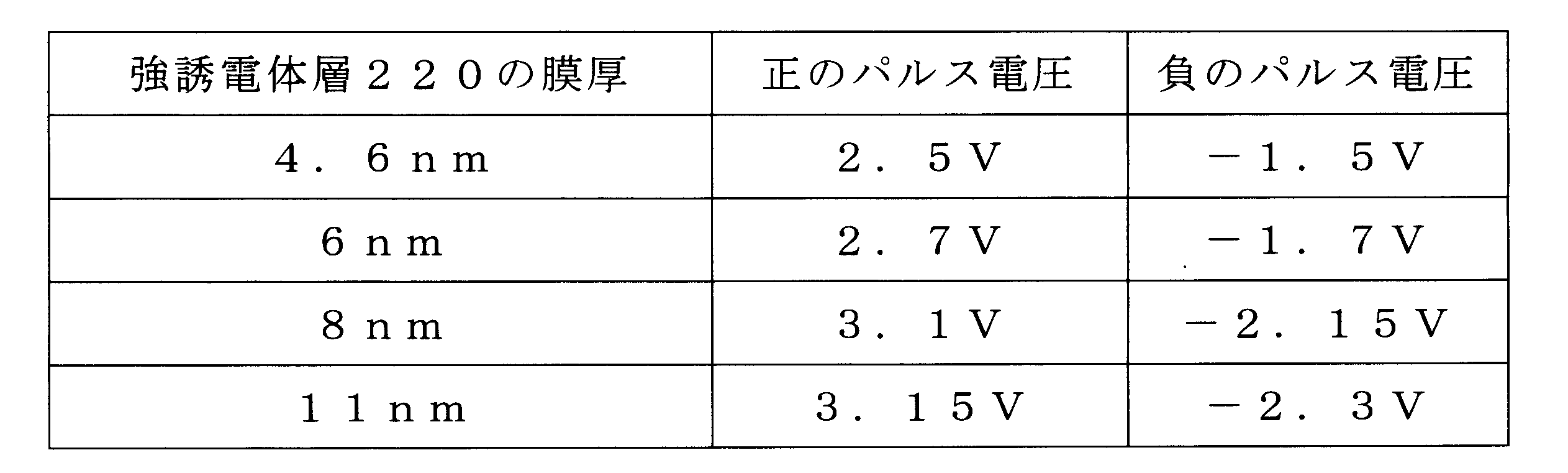
図6の上のグラフに示すように、強誘電体層220の膜厚が8nm及び11nmである記憶装置10のサイクル回数(MWが0Vに達するときのサイクル駆動の回数)が約5×10⁴サイクルであるのに対して、強誘電体層220の膜厚が4.6nm及び6nmである記憶装置10のサイクル回数は約105サイクルである。さらに、図6の下のグラフに示すように、強誘電体層220の膜厚が4.6nm及び6nmである記憶装置10のサイクル回数は106サイクルに達している。
上記のように、強誘電体層220の膜厚を薄膜化(4.6nm及び6nm)することによって、相対的に高電圧の条件であっても約105サイクル回数のエンデュランス特性を得ることができた。さらに、記憶装置10に印加するパルス電圧を低電圧化することによって、約106サイクル回数のエンデュランス特性を得ることができた。
[1-6.高電圧駆動と低電圧駆動との境界]
上記の高電圧駆動における高電圧と低電圧駆動における低電圧との境界について説明する。詳細は後述するが、高電圧と低電圧との境界は、強誘電体層220のP-V特性又は強誘電体層220の膜厚に基づいて特定することができる。図38及び図39は、それぞれ本発明の一実施形態に係るFeFETに対する高電圧駆動における高電圧と低電圧駆動における低電圧との境界を示す図である。
上記の高電圧駆動における高電圧と低電圧駆動における低電圧との境界について説明する。詳細は後述するが、高電圧と低電圧との境界は、強誘電体層220のP-V特性又は強誘電体層220の膜厚に基づいて特定することができる。図38及び図39は、それぞれ本発明の一実施形態に係るFeFETに対する高電圧駆動における高電圧と低電圧駆動における低電圧との境界を示す図である。
まず、高電圧と低電圧との境界を強誘電体層220のP-V特性に基づいて特定する方法について説明する。この場合、まずは強誘電体層220のP-V特性から抗電圧Vcが導出される。抗電圧Vcは、分極(電気双極子)がある方向を向いた状態からその反対の方向を向いた状態に切り替わり始めるために必要な電圧である。つまり、抗電圧Vcは、例えば後述する図8に示すP-V特性において、ゲート電圧Vgを負電圧から正電圧に走査した場合における、上記のニュートラル電圧と、分極の値が負の値から上昇してゼロになったときの電圧との差に相当する。
表1及び表2に示す正のパルス電圧と負のパルス電圧との差を「書き込み電圧の範囲」と表現した場合、高電圧と低電圧との境界は抗電圧Vcに係数3.4を乗じた値によって特定される、という規則性があることが確認されている。つまり、当該境界に基づいて、高電圧に区分される書き込み電圧の範囲と抗電圧Vcとの関係、及び低電圧に区分される書き込み電圧の範囲と抗電圧Vcとの関係は、それぞれ以下のような規則性があることが確認されている。
・高電圧に区分される書き込み電圧の範囲>3.4×Vc
・低電圧に区分される書き込み電圧の範囲<3.4×Vc
・高電圧に区分される書き込み電圧の範囲>3.4×Vc
・低電圧に区分される書き込み電圧の範囲<3.4×Vc
図38において、縦軸は書き込み電圧の範囲(Vg,n-Vg,p[V])であり、横軸は強誘電体層220の膜厚(Thickness[nm])である。表1及び表2に基づいて、低電圧に区分される書き込み電圧の範囲は図38において「○」で示されており、高電圧に区分される書き込み電圧の範囲は図38において「×」で示されている。抗電圧Vc×3.4は、図38において「□」で示されている。図38に示すように、強誘電体層220の各膜厚において、抗電圧Vc×3.4「□」より大きい書き込み電圧の範囲は高電圧に区分され、抗電圧Vc×3.4「□」より小さい書き込み電圧の範囲は低電圧に区分される。
次に、高電圧と低電圧との境界を強誘電体層220の膜厚に基づいて特定する方法について説明する。この場合、図39の実線に示すように、高電圧と低電圧との境界は、強誘電体層220の膜厚を関数とする以下の式で導出することができる。
y=-0.03x2+0.7x+1.65
y=-0.03x2+0.7x+1.65
なお、上記の式において「x」は強誘電体層220の膜厚(Thickness[nm])であり、「y」は書き込み電圧の範囲(Vg,n-Vg,p[V])である。図39において、縦軸及び横軸は図38の縦軸及び横軸と同じである。
図39に示すように、強誘電体層220の各膜厚において、上記の式(図39の実線)より大きい書き込み電圧の範囲は高電圧に区分され、上記の式より小さい書き込み電圧の範囲は低電圧に区分される。
[1-7.サイクル駆動による記憶装置10の疲労メカニズム]
図7~図10を用いて、サイクル駆動による記憶装置10の疲労メカニズムについて説明する。従来、強誘電体層を用いたメモリセルに対するサイクル駆動でMWが小さくなる現象(MWの狭小化)は、例えば半導体層200と酸化物絶縁層210との界面及び酸化物絶縁層210と強誘電体層220との界面の劣化に起因すると考えられていた。具体的には、サイクル駆動によってこれらの界面に電荷のトラップ準位が発生し、そのトラップ準位に電荷がトラップされることによってMWの狭小化が起きると考えられていた。そして、この界面劣化は、その後の処理で回復しないという認識が技術常識だった。
図7~図10を用いて、サイクル駆動による記憶装置10の疲労メカニズムについて説明する。従来、強誘電体層を用いたメモリセルに対するサイクル駆動でMWが小さくなる現象(MWの狭小化)は、例えば半導体層200と酸化物絶縁層210との界面及び酸化物絶縁層210と強誘電体層220との界面の劣化に起因すると考えられていた。具体的には、サイクル駆動によってこれらの界面に電荷のトラップ準位が発生し、そのトラップ準位に電荷がトラップされることによってMWの狭小化が起きると考えられていた。そして、この界面劣化は、その後の処理で回復しないという認識が技術常識だった。
本発明に至る過程において、発明者らは、メモリセルに対して高電圧のサイクル駆動を行った場合と低電圧のサイクル駆動を行った場合とでMWの狭小化のメカニズムが異なることをつきとめた。そして、発明者らは、低電圧のサイクル駆動によってMWが小さくなる原因が、従来の技術常識とは異なる強誘電体層の疲労によるものであることを明らかにした。さらに、発明者らは、この強誘電体層の疲労に対する回復方法を確立し、サイクル駆動によって一度小さくなったMWを回復によって大きくすることに成功した。
図7は、本発明の一実施形態に係るFeFETに対して低電圧駆動又は高電圧駆動を行った場合におけるId-Vg特性の変化を示す図である。図7に示すId-Vg特性は、サイクル駆動開始前のId-Vg特性(実線;Initial)及びサイクル駆動後のId-Vg特性(破線;After cycling)である。図7の上のグラフは、高電圧サイクル(High Voltage)前後のId-Vg特性を示し、下のグラフは、低電圧サイクル(Low Voltage)前後のId-Vg特性を示す。図7に示すId-Vg特性は、強誘電体層220の膜厚が6nmである記憶装置10のId-Vg特性である。つまり、高電圧サイクルにおける正のパルス電圧は3.1Vであり、負のパルス電圧は-2.1Vである。一方、低電圧サイクルにおける正のパルス電圧は2.7Vであり、負のパルス電圧は-1.7Vである。図7に示すId-Vg特性は、ゲート電極230に1μsecのパルス電圧を印加することで電気双極子の向きを変化させたあと、同じゲート電極に0.1secのVgのスキャンを行ってId-Vg特性を評価している。このようにVgのスキャンを行うことで、Id-Vg特性の評価中における強誘電体層220の分極特性への影響は小さい。このようなId-Vg特性を「ファストId-Vg」という場合がある。
図7に示す実線/点線の直角三角形の斜線は、サイクル駆動前/後のId-Vg特性において、閾値電圧付近の傾きを示す。図7の上のグラフに示すように、高電圧サイクル前後のId-Vg特性において、MWの狭小化とともにS値が大きく変化している。実線及び点線の直角三角形の斜線から判るように、高電圧サイクル前に比べて、高電圧サイクル後のS値は大きい。つまり、高電圧サイクルによって、Id-Vg特性における電流値の立ち上がりが緩やかになっている。一方、図7の下のグラフに示すように、低電圧サイクル前後のId-Vg特性において、MWが狭小化しているにも拘わらずS値はほとんど変化していない。このような現象から、低電圧サイクルによるMWの狭小化のメカニズムは、高電圧サイクルによるMWの狭小化のメカニズムと異なると考えられる。
そこで、高電圧サイクル及び低電圧サイクルの各々の前後でP-V特性を測定し、強誘電体層220の分極特性を調べた結果を図8に示す。図8は、本発明の一実施形態に係るFeFETに対して低電圧駆動又は高電圧駆動を行った場合におけるP-V特性の変化を示す図である。図8に示すP-V特性は、サイクル駆動開始前のP-V特性(実線;Initial)とサイクル駆動後のP-V特性(破線;After cycling)である。各P-V特性を示すグラフの横軸はゲート電圧Vg[V]であり、縦軸は分極Polarization[μC/cm2]である。図8の上のグラフ(High Voltage)は、高電圧サイクル前後のP-V特性を示し、下のグラフ(Low Voltage)は、低電圧サイクル前後のP-V特性を示す。図8に示すP-V特性は、強誘電体層220の膜厚が6nmである記憶装置10のP-V特性である。高電圧サイクル及び低電圧サイクルにおけるパルス電圧は図7で説明したパルス電圧と同じである。
図8の上のグラフに示すように、高電圧サイクルの前後でP-V特性の大きな変化はない。一方、図8の下のグラフに示すように、低電圧サイクルの前後でP-V特性は大きく変化している。つまり、低電圧サイクルによって強誘電体層220の分極特性に変化が生じている。このような現象を強誘電体の「疲労」という。強誘電体の疲労は分極反転の繰り返しによって、残留分極の電荷量が低下することに起因すると考えられる。
高電圧サイクルによって記憶装置10に印加されるパルス電圧は、従来のメモリセルに対するパルス電圧と同じである。したがって、高電圧サイクルによって生じるMWの狭小化は、図9に示すように、半導体層200と酸化物絶縁層210との界面及び酸化物絶縁層210と強誘電体層220との界面に発生する電荷のトラップ準位(図9の「×」)によって起きていると考えられる。なお、図9は、本発明の一実施形態に係るFeFETに対して高電圧駆動を行った場合におけるFeFETのMWの狭小化のメカニズムを示す図である。図7に示すように、高電圧サイクルの後にS値が大きくなる現象は、ドレイン電流Idの立ち上がり付近で半導体層200と酸化物絶縁層210との界面付近に発生した電荷のトラップ準位に電子がトラップされたことに起因すると考えられる。一方、図8に示すように、高電圧サイクルの前後でP-V特性はほとんど変化していないことから、高電圧サイクルによって強誘電体層220の疲労は起きていないと考えられる。
一方、図7に示すように、低電圧サイクルの前後でS値はほとんど変化していない。したがって、低電圧サイクルによって生じるMWの狭小化は、上記の界面劣化に起因するものではないと考えられる。図8に示すように、低電圧サイクルの前後でP-V特性が大きく変化したことから、図10に示すように、低電圧サイクルによって強誘電体層220に疲労が起きたと考えられる。したがって、低電圧サイクルによって生じるMWの狭小化は、強誘電体層220の疲労によって起きたと考えられる。なお、図10は、本発明の一実施形態に係るFeFETに対して低電圧駆動を行った場合におけるFeFETのMWの狭小化のメカニズムを示す図である。
上記のように、発明者らは、本発明に至る過程において、低電圧サイクルによるMWの狭小化のメカニズムが高電圧サイクルによるMWの狭小化のメカニズムとは異なることをつきとめた。さらに、発明者らは、低電圧サイクルによるMWの狭小化が強誘電体層の疲労によるものであることを明らかにした。
[1-8.強誘電体層220の疲労の回復動作]
図11を用いて、強誘電体層220の疲労の回復動作について説明する。図11は、本発明の一実施形態に係るFeFETに対するサイクル駆動後の回復動作の概略を示す図である。図11において、「P」はプログラム動作に相当する正のパルス電圧を示す。「R」は読み出し動作(ファストId-Vgの測定)に相当する印加電圧を示す。「E」は消去動作に相当する負のパルス電圧を示す。正のパルス電圧及び負のパルス電圧のパルス幅はともに1μsecである。「cycle1」は、1回目のサイクル駆動を示す。「cycle2」は、2回目のサイクル駆動を示す。「Recovory」は、回復動作を示す。
図11を用いて、強誘電体層220の疲労の回復動作について説明する。図11は、本発明の一実施形態に係るFeFETに対するサイクル駆動後の回復動作の概略を示す図である。図11において、「P」はプログラム動作に相当する正のパルス電圧を示す。「R」は読み出し動作(ファストId-Vgの測定)に相当する印加電圧を示す。「E」は消去動作に相当する負のパルス電圧を示す。正のパルス電圧及び負のパルス電圧のパルス幅はともに1μsecである。「cycle1」は、1回目のサイクル駆動を示す。「cycle2」は、2回目のサイクル駆動を示す。「Recovory」は、回復動作を示す。
回復動作において、強誘電体層220の膜厚が4.6nmである場合、20秒の間に、-2Vから3Vまでの昇圧及び3Vから-2Vまでの降圧が実行される。強誘電体層220の膜厚が6nm、8nm、又は11nmである場合、22秒の間に、-2Vから3.5Vまでの昇圧及び3.5Vから-2Vまでの降圧が実行される。図11の例では、回復動作が実行される時間が秒オーダーであるが、図11に示す回復動作は試験的な処理であり、詳細は後述するが、現実的にはもっと短い時間で回復動作を行うことができる。
1回目のサイクル駆動の前に実行されるプログラム動作、消去動作、及びこれらの動作後の読み出し動作によって、後述する図12の初期(Initial)のId-Vg特性が得られる。1回目のサイクル駆動では、正のパルス電圧及び負のパルス電圧が交互に印加され、所定の回数毎に読み出し動作が実行されることでエンデュランス特性が得られる。サイクル駆動は、エンデュランス特性において、MWがゼロと判定されると終了する。1回目のサイクル駆動の後に実行されるプログラム動作、消去動作、及びこれらの動作後の読み出し動作によって、後述する図12のサイクル後(After cycling)のId-Vg特性が得られる。回復動作の後かつ2回目のサイクル駆動の前に実行されるプログラム動作、消去動作、及びこれらの動作後の読み出し動作によって、後述する図12の回復動作後(Recovory)のId-Vg特性が得られる。その後、1回目のサイクル駆動と同様に2回目のサイクル駆動が実行される。
図12は、本発明の一実施形態に係るFeFETに対する高電圧駆動または低電圧駆動後の回復動作によるId-Vg特性の変化を示す図である。図12に示すId-Vg特性は、サイクル駆動開始前のId-Vg特性(細い実線;Initial)、サイクル駆動後のId-Vg特性(細い破線;After cycling)、及び回復動作後のId-Vg特性(太い実線;Recovory)である。図12の上のグラフは、高電圧サイクル(High Voltage)前後のId-Vg特性を示し、下のグラフは、低電圧サイクル(Low Voltage)前後のId-Vg特性を示す。図12に示すId-Vg特性は、強誘電体層220の膜厚が6nmである記憶装置10のId-Vg特性である。つまり、高電圧サイクルにおける正のパルス電圧は3.1Vであり、負のパルス電圧は-2.1Vである。一方、低電圧サイクルにおける正のパルス電圧は2.7Vであり、負のパルス電圧は-1.7Vである。
図12に示すId-Vg特性は、図7と同様にファストId-Vgである。図12に示すグラフにおけるサイクル駆動開始前(Initial)及びサイクル駆動後(After cycling)のId-Vg特性は、図7に示すこれらのId-Vg特性と同じである。図12に示すように、高電圧サイクル及び低電圧サイクルの両方において、回復動作後(Recovory)にMWが大きくなっている。
高電圧サイクル後の回復動作によって回復したMWは約0.2Vである。低電圧サイクル後の回復動作によって回復したMWは約0.4Vである。ただし、低電圧サイクル前後のMWの変化は、高電圧サイクル前後のMWの変化に比べて小さい。つまり、低電圧サイクルの方が回復動作による効果が高い。このように、低電圧サイクルによるMWの狭小化は、上記の回復動作によって回復可能である。つまり、強誘電体層220の疲労は上記の回復動作で回復可能である。
図13は、本発明の一実施形態に係るFeFETに対する回復動作後のエンデュランス特性を示す図である。図13に示す4つのエンデュランス特性は、いずれも低電圧サイクルによるMWの変化に基づいて得られたエンデュランス特性である。これらのグラフにおいて、横軸はサイクル回数(Cycling number)を示し、縦軸はMWを示す。4つのグラフは、強誘電体層220の膜厚が異なる記憶装置10に対するエンデュランス特性である。左上、右上、左下、及び右下のグラフは、それぞれ強誘電体層220の膜厚が11nm、8nm、6nm、4.6nmである記憶装置10に対するエンデュランス特性である。
サイクル駆動におけるパルス電圧として、各膜厚条件によって表2に示す電圧が印加される。各グラフにおいて、1回目のサイクル駆動(サイクル1)におけるエンデュランス特性(細い破線;Cycle1)、2回目のサイクル駆動(サイクル2)におけるエンデュランス特性(細い実線;Cycle2)、及び3回目のサイクル駆動(サイクル3)におけるエンデュランス特性(太い実線;Cycle3)が表示されている。1回目と2回目のサイクル駆動の間及び2回目と3回目のサイクル駆動の間で、図11に示す回復動作が実行されている。
強誘電体層220の膜厚が11nmである記憶装置10のエンデュランス特性(左上のグラフ)を参照すると、サイクル2及びサイクル3の初期のMWは、サイクル1の初期のMWの半分以下である。さらに、サイクル2及びサイクル3のサイクル回数は、いずれもサイクル1のサイクル回数と比べて約1桁少ない。つまり、この条件では、上記の回復動作を行ってもエンデュランス特性の十分な回復効果を得ることができない。
強誘電体層220の膜厚が8nmである記憶装置10のエンデュランス特性(右上のグラフ)を参照すると、サイクル2及びサイクル3の初期のMWは、サイクル1の初期のMWの半分程度である。さらに、サイクル2及びサイクル3のサイクル回数は、いずれもサイクル1のサイクル回数と比べて少ない。しかし、11nmの条件に比べると、サイクル2及びサイクル3のサイクル回数は多い。つまり、この条件では、上記の回復動作を行ってもエンデュランス特性の十分な回復効果を得ることができないが、11nmの条件に比べると回復効果を得ることができる。
強誘電体層220の膜厚が6nmである記憶装置10のエンデュランス特性(左下のグラフ)を参照すると、サイクル2及びサイクル3の初期のMWは、サイクル1の初期のMWより小さい。しかし、サイクル2及びサイクル3の初期のMWは、上記の11nmの条件及び8nmの条件のサイクル2及びサイクル3の初期のMWより大きい。一方で、サイクル1~サイクル3のサイクル回数には有意差はなく、いずれのサイクルにおいてもサイクル回数は106サイクルに達している。つまり、この条件では、上記の回復動作によってエンデュランス特性の十分な回復効果を得ることができる。
強誘電体層220の膜厚が4.6nmである記憶装置10のエンデュランス特性(右下のグラフ)を参照すると、サイクル2及びサイクル3の初期のMWは、サイクル1の初期のMWより小さい。しかし、6nmの条件に比べると、サイクル回数が増加してもMWは低下しにくい。サイクル2及びサイクル3のサイクル回数はサイクル1のサイクル回数に比べて少なくなっているが、サイクル2及びサイクル3においてもサイクル回数は106サイクルに近い結果が得られている。つまり、この条件では、上記の回復動作によってエンデュランス特性の十分な回復効果を得ることができる。
上記のように、強誘電体層220の膜厚が6nm以下である記憶装置10に対して低電圧サイクルを実行した場合、回復動作によってエンデュランス特性の十分な回復効果を得ることができる。
[1-9.回復動作におけるパルス電圧の印加方法]
図14~図19を用いて、回復動作におけるパルス電圧の印加方法及び各方法による回復動作後のエンデュランス特性を評価した結果について説明する。図14~図16は、本発明の一実施形態に係るFeFETに対するサイクル駆動後の回復動作における回復パルスの極性を示す図である。図17~図19は、本発明の一実施形態に係るFeFETの回復動作後のMWについて、回復パルスの極性依存性、電圧依存性、及びパルス幅依存性を示す図である。なお、図14~図19は、強誘電体層220の膜厚が5.2nmである記憶装置10に対するパルス電圧の印加方法及び評価結果である。回復動作におけるパルス電圧を「回復パルス」という。
図14~図19を用いて、回復動作におけるパルス電圧の印加方法及び各方法による回復動作後のエンデュランス特性を評価した結果について説明する。図14~図16は、本発明の一実施形態に係るFeFETに対するサイクル駆動後の回復動作における回復パルスの極性を示す図である。図17~図19は、本発明の一実施形態に係るFeFETの回復動作後のMWについて、回復パルスの極性依存性、電圧依存性、及びパルス幅依存性を示す図である。なお、図14~図19は、強誘電体層220の膜厚が5.2nmである記憶装置10に対するパルス電圧の印加方法及び評価結果である。回復動作におけるパルス電圧を「回復パルス」という。
図14は、回復動作として「正のパルス電圧(Positive Pulse)」を印加する方法を示す。図14において、回復動作(Recovory)はサイクル1(cycle1)の後に実行される。図14のサイクル1は、図11のサイクル1と同じである。ただし、上記のように、図14~図19で説明する記憶装置10の強誘電体層220の膜厚が5.2nmであり、サイクル1における正のパルス電圧は2.5Vであり、負のパルス電圧は-1.5Vである。図14に示す回復パルスとして、正のパルス電圧のみを強誘電体層220に印加する。回復動作における正のパルス電圧は3Vであり、パルス幅は1μsecである。当該パルス波形は略矩形である。
図15は、回復動作として「負のパルス電圧(Negative Pulse)」を印加する方法を示す。図15に示す回復パルスとして、負のパルス電圧のみを強誘電体層220に印加する。この点を除き、図15に示す印加方法は図14の印加方法と同じである。回復動作における負のパルス電圧は-2Vであり、パルス幅は1μsecである。当該パルス波形は略矩形である。
図16は、回復動作として「バイポーラパルス電圧(Bipolar Pulse)」を印加する方法を示す。図16に示す回復パルスとして、正のパルス電圧及び負のパルス電圧を強誘電体層220に交互に印加する。この点を除き、図16に示す印加方法は図14の印加方法と同じである。回復動作における正のパルス電圧は3Vであり、負のパルス電圧は-2Vであり、これらのパルス幅は1μsecである。当該パルス波形は略矩形である。
図17は、図14~図16に示す回復動作におけるパルス電圧(回復パルス)について評価した結果を示す。図17は、サイクル駆動後に、特定のパルス数で回復動作を行ったあとのMWを示す。図17のグラフにおいて、一番左のプロットはサイクル駆動開始前(Initial)のMWを示し、左から二番目のプロットはサイクル駆動後(After cycling)のMWを示す。左から三番目以降(パルス数(Pulse number)が1(1.E+00)以降)のプロットは、それぞれ所定回数のパルス電圧を印加した後に測定されたMWを示す。図17において、「○」はバイポーラパルス電圧を印加した場合の評価結果を示す。「□」は負のパルス電圧を印加した場合の評価結果を示す。「×」は正のパルス電圧を印加した場合の評価結果を示す。各条件において、正のパルス電圧又は負のパルス電圧が1回印加されると、パルス数が1カウントされる。なお、1回のバイポーラパルス電圧には、正のパルス電圧及び負のパルス電圧が1回ずつ含まれるため、バイポーラパルス電圧の最小パルス数は2である。
図17に示すように、回復動作においてバイポーラパルス電圧を印加した条件で最もMWが大きくなる結果が得られた。一方、正のパルス電圧を印加した条件で最もMWが小さくなる結果が得られた。回復動作においてバイポーラパルス電圧を印加した条件及び負のパルス電圧を印加した条件では、狭小化したMWを効率的に回復することができる。特に、バイポーラパルス電圧を印加した条件では、パルス数が2(2.E+0)だけで顕著なMWの回復効果が得られている。一方、回復動作において正のパルス電圧を印加した条件では、0から104回のパルス電圧を印加した場合において、最大でも0.1V程度のMWの回復効果しか得られなかった。つまり、回復動作において、バイポーラパルス電圧を印加することで、良好なMWを得ることができる。
図18は、回復動作においてバイポーラパルス電圧を印加する方法において、正のパルス電圧及び負のパルス電圧について電圧依存性を評価した結果を示す。図18において、回復動作における[正のパルス電圧/負のパルス電圧]は[2.7V/-1.7V]、[3V/-2V]、及び[3.3V/-2.3V]である。これらのパルス幅は1μsecである。図18において、「□」は、回復動作におけるパルス電圧として[3.3V/-2.3V]が印加された場合の評価結果を示す。「○」は、パルス電圧として[3V/-2V]が印加された場合の評価結果を示す。「×」は、パルス電圧として[2.7V/-1.7V]が印加された場合の評価結果を示す。
図18に示すように、[2.7V/-1.7V]の条件における回復動作後のMWに比べて[3V/-2V]及び[3.3V/-2.3V]の条件における回復動作後のMWの方が大きい結果が得られた。つまり、回復動作において、正のパルス電圧として3V以上の電圧を印加し、負のパルス電圧として-2V以下の電圧を印加することで、良好なMWを得ることができる。
上記の正のパルス電圧を「第1パルス電圧」といい、負のパルス電圧を「第2パルス電圧」という場合がある。また、第1パルス電圧によって印加される電圧を「第1電圧」といい、第2パルス電圧によって印加される電圧を「第2電圧」という場合がある。この場合、上記のように回復動作後に良好なMWを得るためのパルス電圧の条件を以下のように表現することができる。第1電圧は正極性であり、第1電圧の絶対値は3.0V以上である。第2電圧は負極性であり、第2電圧の絶対値は2.0V以上である。
なお、酸化物絶縁層210及び強誘電体層220の耐圧を考慮すると、第1電圧及び第2電圧の絶対値は8.0V以下であることが好ましい。つまり、正のパルス電圧は3.0V以上8.0V以下であることが好ましい。負のパルス電圧は-8.0V以上-2.0V以下であることが好ましい。
図19は、回復動作においてバイポーラパルス電圧を印加する方法において、パルス幅依存性を評価した結果を示す。図19において、回復動作における[正のパルス電圧/負のパルス電圧]は[2.7V/-1.7V]であり、各パルス電圧のパルス幅は1μsec、10μsec、100μsec、及び1msecである。図19において、「◇」は、パルス幅が1msecである場合の評価結果を示す。「○」は、パルス幅が100μsecである場合の評価結果を示す。「□」は、パルス幅が10μsecである場合の評価結果を示す。「△」は、パルス幅が1μsecである場合の評価結果を示す。
図19に示すように、パルス幅が大きいほど回復動作後のMWが大きい傾向があるが、パルス幅が1μsec~1msecの範囲では、パルス幅に対するMWの変化は大きくはなく、いずれの条件においても良好なMWを得ることができる。なお、図19におけるパルス幅の最小値は1μsecであるが、本実施形態において回復動作の効果が得られるパルス幅は0.1μsec以上である。なお、パルス幅は、0.2μsec以上、0.3μsec以上、又は0.5μsec以上であってもよい。
図17に示す結果から、回復動作において、負の電圧を強誘電体層220に印加することでMWの回復効果を得ることができる。さらに、負のパルス電圧と正のパルス電圧とを交互に繰り返し強誘電体層220に印加することで、より高いMWの回復効果を得ることができる。
図19の結果からも判るように、回復動作による強誘電体層220の疲労回復の効果は、強誘電体層220に印加されるパルス電圧の総時間の影響を受ける。したがって、例えば、正のパルス電圧の印加回数をm回(mは1以上の整数)、負のパルス電圧の印加回数をn回(nは1以上の整数)とし、正のパルス電圧のパルス幅をaμsec、負のパルス電圧のパルス幅をbμsecとすると、回復動作に適した条件は「式1」及び「式2」のように表すことができる。
0.1μsec≦a×m<250μsec (式1)
0.1μsec≦b×n<250μsec (式2)
0.1μsec≦a×m<250μsec (式1)
0.1μsec≦b×n<250μsec (式2)
a×mの値が式1の下限未満であり、b×nの値が式2の下限未満である場合、強誘電体層220の疲労回復が不十分であり、MWが十分に回復しない。a×mの値が式1の上限以上であり、b×nの値が式2の上限以上である場合、後述するメモリシステム20において、回復動作にかかる時間が長くなってしまうため、ユーザに不快感を与えてしまう。
上記のように、強誘電体層220の膜厚が3nmより大きく7nmより小さいことで、低電圧のサイクル駆動が可能になるため、エンデュランス特性が高い記憶装置10を実現することができる。さらに、低電圧のサイクル駆動によってMWが狭小化した場合であっても、回復動作におけるパルス電圧として、バイポーラパルス電圧が印加され、当該バイポーラパルス電圧における正のパルス電圧が3V以上であり、負のパルス電圧が-2V以下であり、これらのパルス電圧のパルス幅が0.1μsec以上であることで、狭小化したMWを回復(大きく)することができ、回復動作後であってもエンデュランス特性が高い記憶装置10を実現することができる。
[2.第2実施形態]
図20~図24を用いて、第1実施形態で説明した記憶装置10が用いられたメモリチップ300について説明する。
図20~図24を用いて、第1実施形態で説明した記憶装置10が用いられたメモリチップ300について説明する。
[2-1.メモリチップ300の構成]
図20は、本発明の一実施形態に係るメモリセルアレイの概略図である。図20に示すように、メモリチップ300は、メモリセルアレイ310及び周辺回路320を備える。周辺回路320は、メモリセルアレイ310の周辺に設けられている。本実施形態では、周辺回路320は、メモリセルアレイ310のX方向及びY方向に設けられている。
図20は、本発明の一実施形態に係るメモリセルアレイの概略図である。図20に示すように、メモリチップ300は、メモリセルアレイ310及び周辺回路320を備える。周辺回路320は、メモリセルアレイ310の周辺に設けられている。本実施形態では、周辺回路320は、メモリセルアレイ310のX方向及びY方向に設けられている。
メモリセルアレイ310は、Y方向に配列された複数のメモリブロックMB0~MBjを備える(jは自然数である)。メモリブロックMB0~MBjの各々は、複数のページを備えている。各ページには、上記の記憶装置10を備えたメモリセルがマトリクス状に配置されている。ページはデータの読み出し動作及びプログラム動作を実行する単位である。一方、メモリブロックMBi(iは0以上j以下の整数である)はデータの消去動作を実行する単位である。
周辺回路320は、外部から受信した命令に応じて電圧を生成し、生成された電圧をメモリセルアレイ310に印加することで、当該命令によって指定されたページ又はメモリブロックに対するプログラム動作、読み出し動作、又は消去動作を実行する。
図21は、本発明の一実施形態に係るメモリセルアレイの回路図である。図21に示す回路図は、1つのメモリブロックMBiの構成を示す等価回路図である。メモリブロックMBiは、メモリセルMC、選択トランジスタSTD、STS、ビット線BL(BL1~BLm)、ソース線SL、ワード線WL(WL1~WLn)、及び選択ゲート線SGD、SGSを備えている。メモリセルMCとして、第1実施形態で説明した記憶装置10が用いられる。なお、m及びnは2以上の自然数である。
メモリセルMC及び選択トランジスタSTD、STSは、ビット線BLとソース線SLとの間で直接に接続されている。このように、ビット線BLとソース線SLとの間で直接に接続された複数のメモリセルMCをメモリストリングという場合がある。
周辺回路320がビット線BL、ソース線SL、ワード線WL、及び選択ゲート線SGD、SGSに供給される電圧を制御することで、命令によって指定されたページ又はメモリブロックに対するプログラム動作、読み出し動作、又は消去動作が実行される。
[2-2.メモリシステム20の構成]
図22は、本発明の一実施形態に係るメモリシステムの概略図である。図22に示すように、メモリシステム20は、メモリチップ300及びメモリコントローラ400を含む。メモリコントローラ400はホスト500と通信し、ホスト500からの命令に基づいてメモリチップ300を制御する。
図22は、本発明の一実施形態に係るメモリシステムの概略図である。図22に示すように、メモリシステム20は、メモリチップ300及びメモリコントローラ400を含む。メモリコントローラ400はホスト500と通信し、ホスト500からの命令に基づいてメモリチップ300を制御する。
メモリコントローラ400は、論物変換テーブル410、MPU420、動作回数保持部430、ECC回路440、及びエラー率保持部450を備えている。論物変換テーブル410は、ホスト500から受信した命令に含まれる論理アドレスと、メモリセルアレイ310の各ページに割り当てられた物理アドレスとを関連付けて保持する。動作回数保持部430は、メモリブロックMBi又はページに対応する物理アドレスと、メモリブロックMBi又はページに対して実行されたプログラム動作、読み出し動作、又は消去動作の回数とを関連付けて保持する。ECC回路440は、メモリチップ300から読み出されたデータの誤りを検出し、データに誤りがある場合、データの訂正を行う。エラー率保持部450は、メモリブロックMBi又はページに対応する物理アドレスと、メモリブロックMBi又はページに対応するビットエラー率とを関連付けて保持する。当該ビットエラー率は、各ページについて算出されたビットエラー率の平均値であってもよく、その最大値であってもよい。MPU420は、論物変換テーブル410、動作回数保持部430、ECC回路440、及びエラー率保持部450と協働してメモリチップ300の制御を行う。メモリコントローラ400又はMPU420を制御回路という場合がある。この場合、制御回路がメモリセルアレイ310を制御する、ということができる。
[2-3.メモリシステム20の動作]
図23は、本発明の一実施形態に係るメモリシステムの回復動作を示すフローチャートである。図23に示すフローチャートにおける各ステップは、メモリコントローラ400の論物変換テーブル410、MPU420、動作回数保持部430、ECC回路440、及びエラー率保持部450が協働することで実行される。
図23は、本発明の一実施形態に係るメモリシステムの回復動作を示すフローチャートである。図23に示すフローチャートにおける各ステップは、メモリコントローラ400の論物変換テーブル410、MPU420、動作回数保持部430、ECC回路440、及びエラー率保持部450が協働することで実行される。
まず、メモリコントローラ400がホスト500からプログラム命令又は消去命令を受信すると(ステップS1101;プログラム/消去コマンド)、MPU420は、当該命令によって指定された論理アドレスに基づき、プログラム可能又は消去対象のメモリブロックMBi又はページに対応する物理アドレスを取得する(ステップS1102;物理アドレス取得)。次に、MPU420は、取得した物理アドレス及びプログラム命令又は消去命令をメモリチップ300に送信し、プログラム動作又は消去動作を実行する(ステップS1103;プログラム/消去命令)。次に、MPU420は、動作回数保持部430を参照して、上記の動作を実行した物理アドレスに対応するメモリブロックMBi又はページのプログラム回数又は消去回数を更新する(ステップS1104;プログラム/消去回数更新)。
続いて、MPU420は、更新された動作回数保持部430を参照して、更新後のメモリブロックMBi又はページ(に含まれるメモリセル)に対するプログラム動作又は消去動作の実行回数が所定数(閾値)に達したか否かを判定する(ステップS1105;≧閾値?)。S1105で当該実行回数が閾値に達していると判定した場合(S1105の「Yes」)、MPU420はメモリチップ300に対して第1実施形態で説明した回復動作を実行させる(ステップS1106;回復動作実行)。一方、S1105で上記実行回数が閾値未満であれば(S1105の「No」)、MPU420は図23のフローチャートを終了する。
回復動作は、第1極性の第1電圧と、第1極性とは逆の第2極性の第2電圧と、を強誘電体層220に印加する電圧供給動作である。第1実施形態の図16では、第1極性が正極性であり、第1電圧が正のパルス電圧である。正極性において、プログラム動作における最大電圧(2.5V)より大きい3Vのパルス電圧が供給される。一方、図16では、第2極性が負極性であり、第2電圧が負のパルス電圧である。負極性において、消去動作における最大電圧(-1.5V)より大きい-2Vのパルス電圧が供給される。なお、上記の正極性又は負極性における電圧の大小関係は、各動作における電圧の絶対値の大小関係を意味する。つまり、仮にプログラム動作において負の電圧(例えば、-2.5V)が印加され、消去動作において正の電圧(例えば1.5V)が印加される場合、第1極性が負極性であり、第1電圧が負のパルス電圧であり、第1極性の第1電圧として-3Vのパルス電圧が供給され、第2極性の第2電圧として2Vのパルス電圧が供給される。
図24は、本発明の一実施形態に係るメモリシステムの回復動作を示すフローチャートである。図24に示すフローチャートにおける各ステップは、図23の各ステップと同様に、メモリコントローラ400の論物変換テーブル410、MPU420、動作回数保持部430、ECC回路440、及びエラー率保持部450が協働することで実行される。
図24のフローチャートのうちステップS1201~S1203は、図23のS1101~S1103と同じなので、説明を省略する。ただし、MPU420は、S1201~S1203の前における読み出し動作において、メモリチップ300から受信したデータをECC回路440に送信し、このデータのビットエラー率を取得する(ステップS1200;読み出し・ビットエラー率取得)。ECC回路440は、取得したビットエラー率を適切な物理アドレスと関連付けてエラー率保持部450に保持させる。
S1203の次に、MPU420は、プログラム動作又は消去動作を実行した後で、エラー率保持部450を参照し、プログラム動作又は消去動作を実行したメモリブロックMBi又はページのビットエラー率が所定の確率(閾値)に達しているか否かを判定する(ステップS1204;≧閾値?)。S1204で当該ビットエラー率が閾値に達していると判定した場合(S1204の「Yes」)、MPU420はメモリチップ300に対して第1実施形態で説明した回復動作を実行させる(ステップS1205;回復動作実行)。一方、S1204で上記ビットエラー率が閾値未満であれば(S1204の「No」)、MPU420は図24のフローチャートを終了する。
[3.第3実施形態]
図36を用いて、本発明の一実施形態に係る記憶装置10の構成について説明する。以下の実施形態では、第1実施形態と同様に、メモリ機能を備える層として強誘電体層が用いられた記憶装置30が例示されている。記憶装置30は、チャネルとして機能する層に酸化物半導体層が用いられたFeFETである。
図36を用いて、本発明の一実施形態に係る記憶装置10の構成について説明する。以下の実施形態では、第1実施形態と同様に、メモリ機能を備える層として強誘電体層が用いられた記憶装置30が例示されている。記憶装置30は、チャネルとして機能する層に酸化物半導体層が用いられたFeFETである。
図36は、本発明の一実施形態に係るFeFETを示す概略断面図である。図36に示すように、記憶装置30は、基板110、ゲート電極120、強誘電体層130、チャネル層140、保護絶縁層150、ソース電極170及びドレイン電極180を含む。ゲート電極120は基板110の上に設けられている。チャネル層140はゲート電極120と対向する位置に設けられている。強誘電体層130はゲート電極120とチャネル層140との間に設けられている。保護絶縁層150はチャネル層140の上において、チャネル層140のパターン端部を覆うように設けられている。保護絶縁層150にはチャネル層140に達する開口が設けられている。その開口にソース電極170及びドレイン電極180が設けられている。
基板110として、半導体基板又は絶縁性基板が用いられる。半導体基板として、例えばシリコン基板又はSOI基板が用いられる。絶縁性基板として、例えばガラス基板又は石英基板が用いられる。ゲート電極120、ソース電極170、及びドレイン電極180として、一般的な金属材料が用いられる。例えば、ゲート電極120、ソース電極170、及びドレイン電極180として、モリブデン、タングステン、チタン、及びアルミニウムなどの材料が用いられる。
強誘電体層130として、例えばHZOを用いることができる。強誘電体層130として、ハフニウム及び酸素に加えて、少なくともシリコン、マグネシウム、アルミニウム、バリウム、ジルコニウム、ガドリニウム、ランタン、サマリウム、窒素、及びイットリウムのいずれかを含む層が用いられてもよい。なお、基板110に含まれる不純物がチャネル層140に拡散することを抑制するために、基板110と強誘電体層130との間に、当該不純物の拡散を抑制するバリア層が設けられていてもよい。当該バリア層として、例えば窒化シリコンが用いられてもよい。
チャネル層140として、酸化物半導体が用いられる。酸化物半導体として、インジウム、ガリウム、及び亜鉛を含む酸化物半導体(IGZO)、インジウム、錫、及び亜鉛を含む酸化物半導体(ITZO)、インジウム及び亜鉛を含む酸化物半導体(IZO)、インジウム及び錫を含む酸化物半導体(ITO)、又は酸化インジウムが用いられる。
保護絶縁層150として、一般的な絶縁性材料が用いられる。例えば、保護絶縁層150として、酸化シリコン、窒化シリコン、酸化アルミニウム、及び窒化アルミニウムなどの無機絶縁層が用いられる。保護絶縁層150として、ポリイミド基板、アクリル基板、シロキサン基板、及びフッ素樹脂基板などの有機絶縁層が用いられてもよい。保護絶縁層150は、上記の材料が積層された構造であってもよい。
図36に示す記憶装置30では、強誘電体層130の膜厚を1nmより大きく30nmより小さくすることができる。強誘電体層130の膜厚が上記の範囲であれば、第1実施形態の記憶装置10に対する低電圧駆動と同様の低電圧駆動を実行することができる。その結果、記憶装置30に対するサイクル駆動によってMWが狭小化した場合であっても、第1実施形態で説明した回復動作によってMWを回復することができる。なお、強誘電体層130の分極特性(強誘電特性)を確保するために、強誘電体層130の膜厚を3nmより大きくしてもよい。さらに、強誘電体層130の膜厚を4nmより大きく15nmより小さくすることで、第1実施形態において強誘電体層220の膜厚が4.6nm以上6nm以下の場合と同様に、回復動作後の良好なエンデュランス特性が得られる。
[4.第4実施形態]
図37を用いて、上記の実施形態とは異なる形態のFeFETについて説明する。第1実施形態及び第3実施形態では、基板の主面に平行な方向に電流が流れる横型のFeFETを例示したが、本実施形態では縦型FeFETについて説明する。
図37を用いて、上記の実施形態とは異なる形態のFeFETについて説明する。第1実施形態及び第3実施形態では、基板の主面に平行な方向に電流が流れる横型のFeFETを例示したが、本実施形態では縦型FeFETについて説明する。
図37は、本発明の一実施形態に係るメモリセルの構成を示す斜視図である。図37に示すように、メモリセルMCは、導電層610、半導体層620、酸化物絶縁層630、及び強誘電体層640を有する。導電層610は、基板の主面に沿って形成されている。つまり、導電層610は、XY平面に拡がっている。導電層610は、Z方向に積層されている。Z方向に隣接する2つの導電層610は絶縁層(図示せず)によって離隔されている。つまり、基板の上には導電層610と絶縁層とが交互に積層されている。
半導体層620は、積層された導電層610及び絶縁層を貫通するメモリホールの内部に設けられる。半導体層620は柱状又は筒状である。図37では、半導体層620が円柱状である構成が例示されているが、半導体層620は多角柱状又は円錐台形であってもよい。半導体層620が筒状である場合、筒状の中空部は酸化シリコンなどのフィラーによって埋められる。酸化物絶縁層630は、半導体層620の周囲に設けられている。強誘電体層640は、酸化物絶縁層630の周囲に設けられている。酸化物絶縁層630は半導体層620に接しており、強誘電体層640は酸化物絶縁層630と導電層610とに接している。なお、半導体層620と酸化物絶縁層630との間に他の層が設けられていてもよい。酸化物絶縁層630と強誘電体層640との間に他の層が設けられていてもよい。強誘電体層640と導電層610との間に他の層が設けられていてもよい。
上記の構成において、半導体層620は、チャネルとして機能する。導電層610は、ゲート電極として機能する。酸化物絶縁層630及び強誘電体層640は、ゲート絶縁層として機能する。つまり、導電層610に電圧を印加すると、酸化物絶縁層630及び強誘電体層640を介して半導体層620に電界が形成され、その電界によって半導体層620にキャリアが生成される。Z方向における半導体層620の両端部に電位差を生じさせることで、電界によって生成されたキャリアがZ方向に移動する。つまり、メモリセルMCは縦方向(Z方向)に電流を流す縦型FeFETである。
図1と図37とを対比すると、導電層610はゲート電極230に対応する。半導体層620は半導体層200に対応する。酸化物絶縁層630は、酸化物絶縁層210に対応する。強誘電体層640は強誘電体層220に対応する。したがって、メモリセルMCは、記憶装置10と同様に動作する。
上記のメモリセルMCがピラー状の半導体層620に沿ってZ方向に複数設けられている。つまり、半導体層620に沿って複数のメモリセルMCが直列に接続されている。
[5.第5実施形態]
以下、本発明に係る一実施形態に関連する研究結果について説明する。
以下、本発明に係る一実施形態に関連する研究結果について説明する。
[タイトル]
HZOスケーリング及びFeFETにおける低電圧駆動による疲労回復:界面劣化から強誘電体の疲労への遷移の証拠。
HZOスケーリング及びFeFETにおける低電圧駆動による疲労回復:界面劣化から強誘電体の疲労への遷移の証拠。
[抄訳]
11nmから4.6nmまで小さくしたHf0.5Zr0.5O2(HZO)を用いたFeFETの膜厚スケーリングについて、メモリ特性及びメモリウインドウ(MW)の狭小化のメカニズムに関して体系的な研究がなされた。HZO膜厚スケーリングは、低電圧駆動、高いIon/Ioff比、低いS値(S.S.)、及び良好なエンデュランスにつながる。サイクル電圧の低下に伴い、支配的な狭小化のメカニズムが界面劣化から、高電圧パルスによって回復する強誘電体の疲労に変化することが初めて確認された。この発見に基づき、薄膜HZOのFeFETにおいて、より効果的な回復動作を利用することによってエンデュランスを改善する方法の提案及び実証を行う。
11nmから4.6nmまで小さくしたHf0.5Zr0.5O2(HZO)を用いたFeFETの膜厚スケーリングについて、メモリ特性及びメモリウインドウ(MW)の狭小化のメカニズムに関して体系的な研究がなされた。HZO膜厚スケーリングは、低電圧駆動、高いIon/Ioff比、低いS値(S.S.)、及び良好なエンデュランスにつながる。サイクル電圧の低下に伴い、支配的な狭小化のメカニズムが界面劣化から、高電圧パルスによって回復する強誘電体の疲労に変化することが初めて確認された。この発見に基づき、薄膜HZOのFeFETにおいて、より効果的な回復動作を利用することによってエンデュランスを改善する方法の提案及び実証を行う。
[序論]
HZOベースのFeFETは、不揮発性メモリ、ロジック、及びAIアクセラレータの有望な候補として認識されている。しかし、高電圧駆動及び低エンデュランス(典型的には<105)を含むさまざまな課題が、それらの適用の大きな妨げとなっている。FeRAMにおけるMFMキャパシタにおいて、HZO膜厚のスケーリングが低電圧化及びエンデュランス改善に対する効果的なアプローチであることが証明されている。さらに、MFMキャパシタにおける疲労による劣化は回復可能であり、エンデュランスも改善可能である。しかし、FeFETにおいて、デバイス特性及びMWの狭小化におけるHZO膜厚のスケーリングの影響について、体系的な研究は、いまだ不足したままである。本研究では、HZO膜厚が11nmから4.6nmの範囲におけるFeFETのメモリ特性の体系的な研究を行い、MWの劣化メカニズムを分析した。そして、低電圧駆動下のFeFETにおいて、新たなMWの回復が確認された。この膜厚スケーリング及び疲労回復によって、より良いエンデュランスを実現することができる。
HZOベースのFeFETは、不揮発性メモリ、ロジック、及びAIアクセラレータの有望な候補として認識されている。しかし、高電圧駆動及び低エンデュランス(典型的には<105)を含むさまざまな課題が、それらの適用の大きな妨げとなっている。FeRAMにおけるMFMキャパシタにおいて、HZO膜厚のスケーリングが低電圧化及びエンデュランス改善に対する効果的なアプローチであることが証明されている。さらに、MFMキャパシタにおける疲労による劣化は回復可能であり、エンデュランスも改善可能である。しかし、FeFETにおいて、デバイス特性及びMWの狭小化におけるHZO膜厚のスケーリングの影響について、体系的な研究は、いまだ不足したままである。本研究では、HZO膜厚が11nmから4.6nmの範囲におけるFeFETのメモリ特性の体系的な研究を行い、MWの劣化メカニズムを分析した。そして、低電圧駆動下のFeFETにおいて、新たなMWの回復が確認された。この膜厚スケーリング及び疲労回復によって、より良いエンデュランスを実現することができる。
[デバイス製作]
図25は、本研究において採用された、TiN/HZO/SiO2 FeFETのプロセスフロー及びTEM像である。ALD HZOの膜厚は、11nm、8nm、6nm、4.6nmである。薄膜HZOにおける最適な界面状態及び強誘電性を得るために、RTA温度は450℃に設定された。
図25は、本研究において採用された、TiN/HZO/SiO2 FeFETのプロセスフロー及びTEM像である。ALD HZOの膜厚は、11nm、8nm、6nm、4.6nmである。薄膜HZOにおける最適な界面状態及び強誘電性を得るために、RTA温度は450℃に設定された。
[低電圧駆動]
図26Aは、FeFETに対するP-V測定の測定機構を示す。図26B~図26Eの結果は、同じ電圧範囲において薄膜であるほど高い2Prであることから分かるように、低電圧駆動に対して有利な低いVcを提供することを示す。Id-Vg特性(図27A~図27D)及び抽出されたMW(図28)は、-0.5V/2Vの低いVg範囲であっても、6nm及び4.6nmのFeFETが、11nm及び8nmのFeFETにおける0.3V及び0.05VのMWよりも大きな0.7V及び0.8VのMWを有することを示す。図29A~図29Dは、1μsのプログラム/消去パルスの条件下におけるVth及びファストId-Vg特性から決定されたMWマッピングを示し、薄膜HZO FeFETが低電圧で動作することを明らかにする。図30(a)は、0.8VのMWにおける、4つの異なるHZO膜厚を有するFeFETのId-Vg曲線を対比する。消去/プログラムパルス電圧は-2.4V/3.2V(11nm)から-1.6V/2.7V(4.6nm)に低減される。さらに、小さいS値(図30(b))に起因して、薄膜HZO FeFETは同じMWにおいて、4.6nm HZO FeFETにおける値が11nmのものにおける値の×9.5という、高いIon/Ioff比を示す。
図26Aは、FeFETに対するP-V測定の測定機構を示す。図26B~図26Eの結果は、同じ電圧範囲において薄膜であるほど高い2Prであることから分かるように、低電圧駆動に対して有利な低いVcを提供することを示す。Id-Vg特性(図27A~図27D)及び抽出されたMW(図28)は、-0.5V/2Vの低いVg範囲であっても、6nm及び4.6nmのFeFETが、11nm及び8nmのFeFETにおける0.3V及び0.05VのMWよりも大きな0.7V及び0.8VのMWを有することを示す。図29A~図29Dは、1μsのプログラム/消去パルスの条件下におけるVth及びファストId-Vg特性から決定されたMWマッピングを示し、薄膜HZO FeFETが低電圧で動作することを明らかにする。図30(a)は、0.8VのMWにおける、4つの異なるHZO膜厚を有するFeFETのId-Vg曲線を対比する。消去/プログラムパルス電圧は-2.4V/3.2V(11nm)から-1.6V/2.7V(4.6nm)に低減される。さらに、小さいS値(図30(b))に起因して、薄膜HZO FeFETは同じMWにおいて、4.6nm HZO FeFETにおける値が11nmのものにおける値の×9.5という、高いIon/Ioff比を示す。
[エンデュランス特性]
図31は、(a)同じ電界及び(b)0.5Vの同じメモリウインドウにおける、異なるHZO膜厚を有するFeFETのエンデュランス特性を示す。同じ電界において、6nm及び4.6nm膜厚のHZO FeFETは、11nm膜厚のもの(5×10⁴)に比べて約2倍のエンデュランス(~105)を示す。また、0.5Vの同じMWにおいて、6nm及び4.6nm膜厚のHZO FeFETのエンデュランスは、11nm膜厚のデバイスよりも大きく、1×10⁶に達している。これらの結果は、HZOスケーリングがFeFETのエンデュランスの改善につながることを示す。
図31は、(a)同じ電界及び(b)0.5Vの同じメモリウインドウにおける、異なるHZO膜厚を有するFeFETのエンデュランス特性を示す。同じ電界において、6nm及び4.6nm膜厚のHZO FeFETは、11nm膜厚のもの(5×10⁴)に比べて約2倍のエンデュランス(~105)を示す。また、0.5Vの同じMWにおいて、6nm及び4.6nm膜厚のHZO FeFETのエンデュランスは、11nm膜厚のデバイスよりも大きく、1×10⁶に達している。これらの結果は、HZOスケーリングがFeFETのエンデュランスの改善につながることを示す。
[MW狭小化のメカニズム及び疲労回復]
FeFETのMW狭小化は、従来、高い駆動電圧によって悪化するMOS界面の劣化に起因すると考えられていた。本研究では、FeFETのMW狭小化を引き起こす、図32B、図32Fに示される高電圧による界面の劣化とは区別される、低い駆動電圧によってもたらされる強誘電体の疲労という、別のメカニズムを新たに特定した。ここで、従来のId-Vg測定に加えて、分極特性を評価するためのFeFETのP-V測定を行った。図32C、図32Dに示す高電圧における及び図32G、図32Hに示す低電圧におけるファスト及びDCのId-Vgから、サイクル後にMWが大きく減少し、S値が大きく悪化することが判明した。一方、図32E及び図32IのP-Vは、高電圧のサイクル後には低下しないが、低電圧のサイクル後に強誘電体分極特性が劇的に低下することを示す。これらの結果は、高電圧サイクルによる、MOS界面の劣化に起因するMW狭小化と同時に、低電圧サイクルによる、強誘電体の疲労に起因する分極特性の低下によるMW狭小化を強く示唆している。
さらに、界面劣化に起因するMW狭小化は回復させることができないのに対して、この強誘電体の疲労によるFeFETのMW狭小化は、MFMキャパシタと同様の方法で、高いVg信号によって回復させることができる。ここで、図32Aに示すように、低下したFeFETを回復させるために、長期間の三角信号が印加される。低電圧サイクル後のFeFETにおけるMW及び分極特性が十分に回復することが判明し(図32G~図32I)、これは強誘電体の疲労が回復可能であることを強く示唆する。これに対して、MW低下及びS値の悪化は、高電圧サイクルに対する回復パルスの後でも未だに観察され(図32C、図32D)、これは界面劣化が回復不可能であることを示す。結果として、MW狭小化は、FeFET内部の異なる位置(強誘電体層の内部又は界面)で発生する、高電圧サイクルにおける界面劣化及び低電圧サイクルにおける強誘電体の疲労という2つの異なるメカニズムを有していると結論付けられる。この事実は、強誘電体が疲労したFeFETに対するMWを復帰させるために、回復パルスを利用することができることを示唆する。
[疲労回復を利用したエンデュランス改善]
図33A~図33Dは、繰り返し回復パルス後のFeFETのエンデュランス特性を初期のMWとともに示す。6nm及び4.6nmのHZO FeFETが1回目及び2回目の回復パルス後に十分回復しており、2回目及び3回目のサイクルにおいて106サイクルのエンデュランスが得られている。それに対して、11nm及び8nmのHZO FeFETでは回復が弱く、回復動作後のMWは0.25V未満であり、サイクル数も106に遠く及ばない。この差は、厚いHZO FeFETにおけるMOS界面の劣化に起因するものである(図34A~図34D)。ここで、厚いHZO FeFETにおいて、S値及びMWは大きく劣化している。HZOにおける電界は、MWが固定されたHZO FeFETでは厚いほど小さく見積もられるため、厚いFeFETにおける深刻な劣化が高電圧駆動に起因する。界面がより改善されることで、FeFETに対して上記の方法を適用することによって、より高いエンデュランスを期待することができる。
図33A~図33Dは、繰り返し回復パルス後のFeFETのエンデュランス特性を初期のMWとともに示す。6nm及び4.6nmのHZO FeFETが1回目及び2回目の回復パルス後に十分回復しており、2回目及び3回目のサイクルにおいて106サイクルのエンデュランスが得られている。それに対して、11nm及び8nmのHZO FeFETでは回復が弱く、回復動作後のMWは0.25V未満であり、サイクル数も106に遠く及ばない。この差は、厚いHZO FeFETにおけるMOS界面の劣化に起因するものである(図34A~図34D)。ここで、厚いHZO FeFETにおいて、S値及びMWは大きく劣化している。HZOにおける電界は、MWが固定されたHZO FeFETでは厚いほど小さく見積もられるため、厚いFeFETにおける深刻な劣化が高電圧駆動に起因する。界面がより改善されることで、FeFETに対して上記の方法を適用することによって、より高いエンデュランスを期待することができる。
[結論]
本研究は図35にまとめられている。膜厚スケーリングは低電圧駆動だけでなく、Ion/Ioff比及びエンデュランスの改善も実現する。さらに、Vgを低減することで、MW狭小化のメカニズムが、回復不可能なMOS界面の劣化から回復可能な強誘電体の疲労に変化することを初めて証明した。この発見に基づいて、このMWの特性回復を利用することでエンデュランスを改善する方法を提案及び実証した。
本研究は図35にまとめられている。膜厚スケーリングは低電圧駆動だけでなく、Ion/Ioff比及びエンデュランスの改善も実現する。さらに、Vgを低減することで、MW狭小化のメカニズムが、回復不可能なMOS界面の劣化から回復可能な強誘電体の疲労に変化することを初めて証明した。この発見に基づいて、このMWの特性回復を利用することでエンデュランスを改善する方法を提案及び実証した。
図35に示すように、強誘電体の疲労及び界面劣化が、それぞれ低電圧サイクル及び高電圧サイクルにおける支配的なMW狭小化のメカニズムであることを解明した。また、強誘電体の疲労は回復可能であることを特定し、これは新たに提唱するFeFET回復の方法につながる。さらに、HZO膜厚スケーリングによってもたらされる低電圧駆動を示す。FeFETの低電圧駆動に基づく、これらの2つの戦略の組み合わせは、高いエンデュランス特性に効果的に寄与する。
[6.第6実施形態]
以下、本発明に係る一実施形態に関連する構成について説明する。第6実施形態に係る構成を特許請求の範囲として記載することができる。
以下、本発明に係る一実施形態に関連する構成について説明する。第6実施形態に係る構成を特許請求の範囲として記載することができる。
[構成要件1]
シリコンを含むチャネル層と、
前記チャネル層と接する界面層と、
前記界面層と接し、酸化ハフニウムを含む強誘電体層と、
前記強誘電体層及び前記界面層を介して前記チャネル層と対向するゲート電極と、を備え、
前記強誘電体層の膜厚は3nmより大きく7nmより小さい強誘電体メモリ装置。
シリコンを含むチャネル層と、
前記チャネル層と接する界面層と、
前記界面層と接し、酸化ハフニウムを含む強誘電体層と、
前記強誘電体層及び前記界面層を介して前記チャネル層と対向するゲート電極と、を備え、
前記強誘電体層の膜厚は3nmより大きく7nmより小さい強誘電体メモリ装置。
[構成要件2]
前記強誘電体層の膜厚は4.6nm以上6nm以下である、構成要件1に記載の強誘電体メモリ装置。
前記強誘電体層の膜厚は4.6nm以上6nm以下である、構成要件1に記載の強誘電体メモリ装置。
[構成要件3]
前記界面層は酸化シリコンを含む、構成要件1に記載の強誘電体メモリ装置。
前記界面層は酸化シリコンを含む、構成要件1に記載の強誘電体メモリ装置。
[構成要件4]
前記界面層の膜厚は5nm未満である、構成要件1に記載の強誘電体メモリ装置。
前記界面層の膜厚は5nm未満である、構成要件1に記載の強誘電体メモリ装置。
[構成要件5]
前記強誘電体層は、ハフニウム及び酸素に加えて、少なくともシリコン、マグネシウム、アルミニウム、バリウム、ジルコニウム、ガドリニウム、ランタン、サマリウム、窒素、及びイットリウムのいずれかを含む、構成要件1に記載の強誘電体メモリ装置。
前記強誘電体層は、ハフニウム及び酸素に加えて、少なくともシリコン、マグネシウム、アルミニウム、バリウム、ジルコニウム、ガドリニウム、ランタン、サマリウム、窒素、及びイットリウムのいずれかを含む、構成要件1に記載の強誘電体メモリ装置。
[構成要件6]
構成要件1に記載の前記強誘電体メモリ装置を含むメモリセルと、
前記メモリセルを制御する制御回路と、を備え、
前記制御回路は、
前記メモリセルに対するプログラム動作又は消去動作の実行回数が所定数に達したか否かを判定し、
前記実行回数が前記所定数に達したと判定した場合、第1極性の第1電圧と、前記第1極性とは逆の第2極性の第2電圧と、を前記強誘電体層に印加する電圧供給動作を実行し、
前記第1電圧は、前記プログラム動作における最大電圧より大きく、
前記第2電圧は、前記消去動作における最大電圧より大きい。
構成要件1に記載の前記強誘電体メモリ装置を含むメモリセルと、
前記メモリセルを制御する制御回路と、を備え、
前記制御回路は、
前記メモリセルに対するプログラム動作又は消去動作の実行回数が所定数に達したか否かを判定し、
前記実行回数が前記所定数に達したと判定した場合、第1極性の第1電圧と、前記第1極性とは逆の第2極性の第2電圧と、を前記強誘電体層に印加する電圧供給動作を実行し、
前記第1電圧は、前記プログラム動作における最大電圧より大きく、
前記第2電圧は、前記消去動作における最大電圧より大きい。
[構成要件7]
構成要件1に記載の前記強誘電体メモリ装置を含む複数のメモリセルと、
前記複数のメモリセルを制御する制御回路と、を備え、
前記制御回路は、
ビットエラー率が所定確率以上か否かを判定し、
前記ビットエラー率が前記所定確率以上であると判定した場合、第1極性の第1電圧と、前記第1極性とは逆の第2極性の第2電圧と、を前記強誘電体層に印加する電圧供給動作を実行し、
前記第1電圧は、前記プログラム動作における最大電圧より大きく、
前記第2電圧は、前記消去動作における最大電圧より大きい。
構成要件1に記載の前記強誘電体メモリ装置を含む複数のメモリセルと、
前記複数のメモリセルを制御する制御回路と、を備え、
前記制御回路は、
ビットエラー率が所定確率以上か否かを判定し、
前記ビットエラー率が前記所定確率以上であると判定した場合、第1極性の第1電圧と、前記第1極性とは逆の第2極性の第2電圧と、を前記強誘電体層に印加する電圧供給動作を実行し、
前記第1電圧は、前記プログラム動作における最大電圧より大きく、
前記第2電圧は、前記消去動作における最大電圧より大きい。
[構成要件8]
金属酸化物を含むチャネル層と、
前記チャネル層と接し、酸化ハフニウムを含む強誘電体層と、
前記強誘電体層を介して前記チャネル層と対向するゲート電極と、を備え、
前記強誘電体層の膜厚は1nmより大きく30nmより小さい強誘電体メモリ装置。
金属酸化物を含むチャネル層と、
前記チャネル層と接し、酸化ハフニウムを含む強誘電体層と、
前記強誘電体層を介して前記チャネル層と対向するゲート電極と、を備え、
前記強誘電体層の膜厚は1nmより大きく30nmより小さい強誘電体メモリ装置。
[構成要件9]
前記強誘電体層の膜厚は4nmより大きく15nmより小さい、構成要件8に記載の強誘電体メモリ装置。
前記強誘電体層の膜厚は4nmより大きく15nmより小さい、構成要件8に記載の強誘電体メモリ装置。
[構成要件10]
前記金属酸化物はIGZO、ITZO、IZO、ITO、又は酸化インジウムである、構成要件8に記載の強誘電体メモリ装置。
前記金属酸化物はIGZO、ITZO、IZO、ITO、又は酸化インジウムである、構成要件8に記載の強誘電体メモリ装置。
[構成要件11]
前記強誘電体層は、ハフニウム及び酸素に加えて、少なくともシリコン、マグネシウム、アルミニウム、バリウム、ジルコニウム、ガドリニウム、ランタン、サマリウム、窒素、及びイットリウムのいずれかを含む、構成要件8に記載の強誘電体メモリ装置。
前記強誘電体層は、ハフニウム及び酸素に加えて、少なくともシリコン、マグネシウム、アルミニウム、バリウム、ジルコニウム、ガドリニウム、ランタン、サマリウム、窒素、及びイットリウムのいずれかを含む、構成要件8に記載の強誘電体メモリ装置。
[構成要件12]
構成要件8に記載の前記強誘電体メモリ装置を含むメモリセルと、
前記メモリセルを制御する制御回路と、を備え、
前記制御回路は、
前記メモリセルに対するプログラム動作又は消去動作の実行回数が所定数に達したか否かを判定し、
前記実行回数が前記所定数に達したと判定した場合、第1極性の第1電圧と、前記第1極性とは逆の第2極性の第2電圧と、を前記強誘電体層に印加する電圧供給動作を実行し、
前記第1電圧は、前記プログラム動作における最大電圧より大きく、
前記第2電圧は、前記消去動作における最大電圧より大きい。
構成要件8に記載の前記強誘電体メモリ装置を含むメモリセルと、
前記メモリセルを制御する制御回路と、を備え、
前記制御回路は、
前記メモリセルに対するプログラム動作又は消去動作の実行回数が所定数に達したか否かを判定し、
前記実行回数が前記所定数に達したと判定した場合、第1極性の第1電圧と、前記第1極性とは逆の第2極性の第2電圧と、を前記強誘電体層に印加する電圧供給動作を実行し、
前記第1電圧は、前記プログラム動作における最大電圧より大きく、
前記第2電圧は、前記消去動作における最大電圧より大きい。
[構成要件13]
構成要件8に記載の前記強誘電体メモリ装置を含む複数のメモリセルと、
前記複数のメモリセルを制御する制御回路と、を備え、
前記制御回路は、
ビットエラー率が所定確率以上か否かを判定し、
前記ビットエラー率が前記所定確率以上であると判定した場合、第1極性の第1電圧と、前記第1極性とは逆の第2極性の第2電圧と、を前記強誘電体層に印加する電圧供給動作を実行し、
前記第1電圧は、前記プログラム動作における最大電圧より大きく、
前記第2電圧は、前記消去動作における最大電圧より大きい。
構成要件8に記載の前記強誘電体メモリ装置を含む複数のメモリセルと、
前記複数のメモリセルを制御する制御回路と、を備え、
前記制御回路は、
ビットエラー率が所定確率以上か否かを判定し、
前記ビットエラー率が前記所定確率以上であると判定した場合、第1極性の第1電圧と、前記第1極性とは逆の第2極性の第2電圧と、を前記強誘電体層に印加する電圧供給動作を実行し、
前記第1電圧は、前記プログラム動作における最大電圧より大きく、
前記第2電圧は、前記消去動作における最大電圧より大きい。
本発明の実施形態として上述した各実施形態(変形例を含む)は、相互に矛盾しない限りにおいて、適宜組み合わせて実施することができる。各実施形態を基にして、当業者が適宜構成要素の追加、削除もしくは設計変更を行ったもの、又は、工程の追加、省略もしくは条件変更を行ったものも、本発明の要旨を備えている限り、本発明の範囲に含まれる。
また、上述した各実施形態の態様によりもたらされる作用効果とは異なる他の作用効果であっても、本明細書の記載から明らかなもの、又は、当業者において容易に予測し得るものについては、当然に本発明によりもたらされるものと解される。
10:記憶装置、 20:メモリシステム、 30:記憶装置、 110:基板、 120:ゲート電極、 130:強誘電体層、 140:チャネル層、 150:保護絶縁層、 170:ソース電極、 180:ドレイン電極、 200:半導体層、 201:低抵抗領域、 202:チャネル領域、 210:酸化物絶縁層、 220:強誘電体層、 230:ゲート電極、 231:第1導電層、 232:第2導電層、 240:層間絶縁層、 250:電極、 300:メモリチップ、 310:メモリセルアレイ、 320:周辺回路、 400:メモリコントローラ、 410:論物変換テーブル、 420:MPU、 430:動作回数保持部、 440:ECC回路、 450:エラー率保持部、 500:ホスト、 BL:ビット線、 MB:メモリブロック、 MC:メモリセル、 MW:メモリウインドウ、 SGD:選択ゲート線、 SGS:選択ゲート線、 SL:ソース線、 STD:選択トランジスタ、 STS:選択トランジスタ、 WL:ワード線
Claims (20)
- 半導体層と、
前記半導体層と対向するゲート電極と、
前記半導体層と前記ゲート電極との間に設けられた絶縁層と、
前記絶縁層と前記ゲート電極との間に設けられ、酸化ハフニウムを含む強誘電体層と、を備え、
前記強誘電体層の膜厚は、3nmより大きく7nmより小さい記憶装置。 - 前記半導体層はシリコンを含み、
前記絶縁層は前記半導体層と接し、
前記強誘電体層は前記絶縁層と接する、請求項1に記載の記憶装置。 - 前記強誘電体層の膜厚は4.6nm以上6nm以下である、請求項2に記載の記憶装置。
- 前記絶縁層は酸化シリコンを含む、請求項2に記載の記憶装置。
- 前記絶縁層の膜厚は5nm未満である、請求項2に記載の記憶装置。
- 前記強誘電体層は、ハフニウム及び酸素に加えて、少なくともシリコン、マグネシウム、アルミニウム、バリウム、ジルコニウム、ガドリニウム、ランタン、サマリウム、窒素、及びイットリウムのいずれかを含む、請求項2に記載の記憶装置。
- 酸化物半導体層と、
前記酸化物半導体層と対向するゲート電極と、
前記酸化物半導体層と前記ゲート電極との間に設けられ、酸化ハフニウムを含む強誘電体層と、を備え、
前記強誘電体層の膜厚は、1nmより大きく30nmより小さい記憶装置。 - 前記強誘電体層の膜厚は4nmより大きく15nm以下より小さい、請求項7に記載の記憶装置。
- 前記酸化物半導体層は、IGZO、ITZO、IZO、ITO、又は酸化インジウムである、請求項7に記載の記憶装置。
- 前記強誘電体層は、ハフニウム及び酸素に加えて、少なくともシリコン、マグネシウム、アルミニウム、バリウム、ジルコニウム、ガドリニウム、ランタン、サマリウム、窒素、及びイットリウムのいずれかを含む、請求項7に記載の記憶装置。
- 請求項1乃至10のいずれか一に記載の記憶装置を備えたメモリセルがマトリクス状に配置されたメモリセルアレイと、
前記メモリセルアレイを制御する制御回路と、を備え、
前記制御回路は、
前記メモリセルに対するプログラム動作又は消去動作の実行回数が所定数に達したか否かを判定し、
前記実行回数が前記所定数に達したと判定した場合、第1極性の第1電圧と、前記第1極性とは逆の第2極性の第2電圧と、を前記強誘電体層に印加する電圧供給動作を実行し、
前記第1電圧は、前記プログラム動作における最大電圧より大きく、
前記第2電圧は、前記消去動作における最大電圧より大きいメモリシステム。 - 前記制御回路は、
前記電圧供給動作において、m回(mは1以上の整数)の第1パルス電圧によって前記第1電圧を前記強誘電体層に印加し、n回(nは1以上の整数)の第2パルス電圧によって前記第2電圧を前記強誘電体層に印加し、
前記第1パルス電圧のパルス幅をa(μsec)とし、前記第2パルス電圧のパルス幅をb(μsec)とした場合に、
0.1μsec≦a×m<250μsec (式1)
0.1μsec≦b×n<250μsec (式2)
式1及び式2が成り立つように、前記第1パルス電圧及び前記第2パルス電圧を前記強誘電体層に印加する、請求項11に記載のメモリシステム。 - 前記第1パルス電圧及び前記第2パルス電圧の波形は略矩形である、請求項12に記載のメモリシステム。
- 前記制御回路は、前記第1パルス電圧と前記第2パルス電圧とを、前記強誘電体層に交互に印加する、請求項12に記載のメモリシステム。
- 前記第1電圧は正極性であり、
前記第1電圧の絶対値は3.0V以上であり、
前記第2電圧は負極性であり、
前記第2電圧の絶対値は2.0V以上である、請求項12に記載のメモリシステム。 - 請求項1乃至10のいずれか一に記載の記憶装置がマトリクス状に配置された複数のメモリセルアレイと、
前記複数のメモリセルアレイを制御する制御回路と、を備え、
前記制御回路は、
プログラム動作又は消去動作を実行した後にビットエラー率が所定確率以上か否かを判定し、
前記ビットエラー率が前記所定確率以上であると判定した場合、第1極性の第1電圧と、前記第1極性とは逆の第2極性の第2電圧と、を前記強誘電体層に印加する電圧供給動作を実行し、
前記第1電圧は、前記プログラム動作における最大電圧より大きく、
前記第2電圧は、前記消去動作における最大電圧より大きいメモリシステム。 - 前記制御回路は、
前記電圧供給動作において、m回(mは1以上の整数)の第1パルス電圧によって前記第1電圧を前記強誘電体層に印加し、n回(nは1以上の整数)の第2パルス電圧によって前記第2電圧を前記強誘電体層に印加し、
前記第1パルス電圧のパルス幅をa(μsec)とし、前記第2パルス電圧のパルス幅をb(μsec)とした場合に、
0.1μsec≦a×m<250μsec (式1)
0.1μsec≦b×n<250μsec (式2)
式1及び式2が成り立つように、前記第1パルス電圧及び前記第2パルス電圧を前記強誘電体層に印加する、請求項16に記載のメモリシステム。 - 前記第1パルス電圧及び前記第2パルス電圧の波形は略矩形である、請求項17に記載のメモリシステム。
- 前記制御回路は、前記第1パルス電圧と前記第2パルス電圧とを、前記強誘電体層に交互に印加する、請求項17に記載のメモリシステム。
- 前記第1電圧は正極性であり、
前記第1電圧の絶対値は3.0V以上であり、
前記第2電圧は負極性であり、
前記第2電圧の絶対値は2.0V以上である、請求項17に記載のメモリシステム。
Priority Applications (4)
| Application Number | Priority Date | Filing Date | Title |
|---|---|---|---|
| CN202480036319.1A CN121286114A (zh) | 2023-06-07 | 2024-05-09 | 存储装置和存储系统 |
| KR1020257035348A KR20260020910A (ko) | 2023-06-07 | 2024-05-09 | 기억 장치 및 메모리 시스템 |
| JP2025525997A JPWO2024252842A1 (ja) | 2023-06-07 | 2024-05-09 | |
| US19/406,338 US20260089969A1 (en) | 2023-06-07 | 2025-12-02 | Memory system and a method for controlling memory system |
Applications Claiming Priority (2)
| Application Number | Priority Date | Filing Date | Title |
|---|---|---|---|
| US202363506675P | 2023-06-07 | 2023-06-07 | |
| US63/506,675 | 2023-06-07 |
Related Child Applications (1)
| Application Number | Title | Priority Date | Filing Date |
|---|---|---|---|
| US19/406,338 Continuation US20260089969A1 (en) | 2023-06-07 | 2025-12-02 | Memory system and a method for controlling memory system |
Publications (1)
| Publication Number | Publication Date |
|---|---|
| WO2024252842A1 true WO2024252842A1 (ja) | 2024-12-12 |
Family
ID=93795222
Family Applications (1)
| Application Number | Title | Priority Date | Filing Date |
|---|---|---|---|
| PCT/JP2024/017271 Ceased WO2024252842A1 (ja) | 2023-06-07 | 2024-05-09 | 記憶装置及びメモリシステム |
Country Status (6)
| Country | Link |
|---|---|
| US (1) | US20260089969A1 (ja) |
| JP (1) | JPWO2024252842A1 (ja) |
| KR (1) | KR20260020910A (ja) |
| CN (1) | CN121286114A (ja) |
| TW (1) | TW202520859A (ja) |
| WO (1) | WO2024252842A1 (ja) |
Citations (4)
| Publication number | Priority date | Publication date | Assignee | Title |
|---|---|---|---|---|
| JP2019160374A (ja) * | 2018-03-15 | 2019-09-19 | 東芝メモリ株式会社 | 半導体記憶装置 |
| WO2021024598A1 (ja) * | 2019-08-08 | 2021-02-11 | 国立研究開発法人科学技術振興機構 | 不揮発性記憶装置及びその動作方法 |
| JP2023040758A (ja) * | 2021-09-10 | 2023-03-23 | ルネサスエレクトロニクス株式会社 | 半導体装置および半導体装置の製造方法 |
| JP2023044116A (ja) * | 2021-09-17 | 2023-03-30 | キオクシア株式会社 | 記憶装置 |
-
2024
- 2024-05-09 JP JP2025525997A patent/JPWO2024252842A1/ja active Pending
- 2024-05-09 WO PCT/JP2024/017271 patent/WO2024252842A1/ja not_active Ceased
- 2024-05-09 CN CN202480036319.1A patent/CN121286114A/zh active Pending
- 2024-05-09 KR KR1020257035348A patent/KR20260020910A/ko active Pending
- 2024-05-10 TW TW113117416A patent/TW202520859A/zh unknown
-
2025
- 2025-12-02 US US19/406,338 patent/US20260089969A1/en active Pending
Patent Citations (4)
| Publication number | Priority date | Publication date | Assignee | Title |
|---|---|---|---|---|
| JP2019160374A (ja) * | 2018-03-15 | 2019-09-19 | 東芝メモリ株式会社 | 半導体記憶装置 |
| WO2021024598A1 (ja) * | 2019-08-08 | 2021-02-11 | 国立研究開発法人科学技術振興機構 | 不揮発性記憶装置及びその動作方法 |
| JP2023040758A (ja) * | 2021-09-10 | 2023-03-23 | ルネサスエレクトロニクス株式会社 | 半導体装置および半導体装置の製造方法 |
| JP2023044116A (ja) * | 2021-09-17 | 2023-03-30 | キオクシア株式会社 | 記憶装置 |
Also Published As
| Publication number | Publication date |
|---|---|
| CN121286114A (zh) | 2026-01-06 |
| TW202520859A (zh) | 2025-05-16 |
| US20260089969A1 (en) | 2026-03-26 |
| KR20260020910A (ko) | 2026-02-12 |
| JPWO2024252842A1 (ja) | 2024-12-12 |
Similar Documents
| Publication | Publication Date | Title |
|---|---|---|
| JP7699821B2 (ja) | 不揮発性記憶装置、不揮発性記憶素子及びその製造方法 | |
| CN102714209B (zh) | 半导体存储器件及其驱动方法 | |
| JP5459999B2 (ja) | 不揮発性半導体記憶素子、不揮発性半導体装置及び不揮発性半導体素子の動作方法 | |
| US7585728B2 (en) | Methods of programming memory cells using manipulation of oxygen vacancies | |
| TW200425408A (en) | Charge-trapping memory arrays resistant to damage from contact hole formation | |
| CN101223640A (zh) | 高密度“与非”非易失性存储器装置 | |
| CN101964209A (zh) | P沟道非易失性存储元件的操作方法 | |
| KR20220034890A (ko) | 비휘발성 기억 장치 및 그 동작 방법 | |
| JP5238208B2 (ja) | 不揮発性半導体記憶装置の駆動方法及び不揮発性半導体記憶装置 | |
| JP2004214365A (ja) | 不揮発性半導体メモリ装置およびその動作方法 | |
| TW200931648A (en) | Non-volatile semiconductor memory device and method of manufacturing the same | |
| JP3802809B2 (ja) | 記憶セルアレイ | |
| US20250273267A1 (en) | Method of operating memory cell | |
| Joh et al. | Dual-port ferroelectric NAND flash memory for large memory window, QLC programmable and disturbance-free operations | |
| EP1894244A2 (en) | Non-volatile memory cells without diffusion junctions | |
| JP4761946B2 (ja) | 不揮発性半導体記憶素子及びその製造方法並びに不揮発性半導体記憶素子を含む半導体集積回路装置 | |
| KR20030064863A (ko) | 메모리 셀의 강유전성 트랜지스터에 대한 상태 판독 및저장 방법 및 메모리 행렬 | |
| US20260089969A1 (en) | Memory system and a method for controlling memory system | |
| KR20010102832A (ko) | 메모리 셀에서 강유전성 트랜지스터로부터 상태를판독하고 강유전성 트랜지스터에 상태를 저장하는 방법 및메모리 매트릭스 | |
| US9042155B2 (en) | Reactive metal implanted oxide based memory | |
| CN100498973C (zh) | 非易失性存储元件的操作方法 | |
| KR20100127109A (ko) | 전하트랩소자를 단위셀로 갖는 낸드 플래시 메모리소자의 프로그램 방법 | |
| JP2001267525A (ja) | 強誘電体不揮発性記憶装置 | |
| JP2011009640A (ja) | 半導体集積回路装置 |
Legal Events
| Date | Code | Title | Description |
|---|---|---|---|
| 121 | Ep: the epo has been informed by wipo that ep was designated in this application |
Ref document number: 24819079 Country of ref document: EP Kind code of ref document: A1 |
|
| ENP | Entry into the national phase |
Ref document number: 2025525997 Country of ref document: JP Kind code of ref document: A |
|
| NENP | Non-entry into the national phase |
Ref country code: DE |
|
| 122 | Ep: pct application non-entry in european phase |
Ref document number: 24819079 Country of ref document: EP Kind code of ref document: A1 |