WO2024224475A1 - ゲート駆動回路 - Google Patents
ゲート駆動回路 Download PDFInfo
- Publication number
- WO2024224475A1 WO2024224475A1 PCT/JP2023/016266 JP2023016266W WO2024224475A1 WO 2024224475 A1 WO2024224475 A1 WO 2024224475A1 JP 2023016266 W JP2023016266 W JP 2023016266W WO 2024224475 A1 WO2024224475 A1 WO 2024224475A1
- Authority
- WO
- WIPO (PCT)
- Prior art keywords
- signal
- gate drive
- gate
- capacitor
- circuit
- Prior art date
- Legal status (The legal status is an assumption and is not a legal conclusion. Google has not performed a legal analysis and makes no representation as to the accuracy of the status listed.)
- Ceased
Links
Images





Classifications
-
- H—ELECTRICITY
- H02—GENERATION; CONVERSION OR DISTRIBUTION OF ELECTRIC POWER
- H02M—APPARATUS FOR CONVERSION BETWEEN AC AND AC, BETWEEN AC AND DC, OR BETWEEN DC AND DC, AND FOR USE WITH MAINS OR SIMILAR POWER SUPPLY SYSTEMS; CONVERSION OF DC OR AC INPUT POWER INTO SURGE OUTPUT POWER; CONTROL OR REGULATION THEREOF
- H02M1/00—Details of apparatus for conversion
- H02M1/08—Circuits specially adapted for the generation of control voltages for semiconductor devices incorporated in static converters
-
- H—ELECTRICITY
- H03—ELECTRONIC CIRCUITRY
- H03K—PULSE TECHNIQUE
- H03K17/00—Electronic switching or gating, i.e. not by contact-making and –breaking
- H03K17/16—Modifications for eliminating interference voltages or currents
- H03K17/161—Modifications for eliminating interference voltages or currents in field-effect transistor switches
- H03K17/162—Modifications for eliminating interference voltages or currents in field-effect transistor switches without feedback from the output circuit to the control circuit
- H03K17/163—Soft switching
-
- H—ELECTRICITY
- H02—GENERATION; CONVERSION OR DISTRIBUTION OF ELECTRIC POWER
- H02M—APPARATUS FOR CONVERSION BETWEEN AC AND AC, BETWEEN AC AND DC, OR BETWEEN DC AND DC, AND FOR USE WITH MAINS OR SIMILAR POWER SUPPLY SYSTEMS; CONVERSION OF DC OR AC INPUT POWER INTO SURGE OUTPUT POWER; CONTROL OR REGULATION THEREOF
- H02M1/00—Details of apparatus for conversion
- H02M1/0003—Details of control, feedback or regulation circuits
- H02M1/0038—Circuits or arrangements for suppressing, e.g. by masking incorrect turn-on or turn-off signals, e.g. due to current spikes in current mode control
-
- H—ELECTRICITY
- H02—GENERATION; CONVERSION OR DISTRIBUTION OF ELECTRIC POWER
- H02M—APPARATUS FOR CONVERSION BETWEEN AC AND AC, BETWEEN AC AND DC, OR BETWEEN DC AND DC, AND FOR USE WITH MAINS OR SIMILAR POWER SUPPLY SYSTEMS; CONVERSION OF DC OR AC INPUT POWER INTO SURGE OUTPUT POWER; CONTROL OR REGULATION THEREOF
- H02M1/00—Details of apparatus for conversion
- H02M1/38—Means for preventing simultaneous conduction of switches
-
- H—ELECTRICITY
- H02—GENERATION; CONVERSION OR DISTRIBUTION OF ELECTRIC POWER
- H02M—APPARATUS FOR CONVERSION BETWEEN AC AND AC, BETWEEN AC AND DC, OR BETWEEN DC AND DC, AND FOR USE WITH MAINS OR SIMILAR POWER SUPPLY SYSTEMS; CONVERSION OF DC OR AC INPUT POWER INTO SURGE OUTPUT POWER; CONTROL OR REGULATION THEREOF
- H02M3/00—Conversion of DC power input into DC power output
- H02M3/02—Conversion of DC power input into DC power output without intermediate conversion into AC
- H02M3/04—Conversion of DC power input into DC power output without intermediate conversion into AC by static converters
- H02M3/06—Conversion of DC power input into DC power output without intermediate conversion into AC by static converters using resistors or capacitors, e.g. potential divider
- H02M3/07—Conversion of DC power input into DC power output without intermediate conversion into AC by static converters using resistors or capacitors, e.g. potential divider using capacitors charged and discharged alternately by semiconductor devices with control electrode, e.g. charge pumps
- H02M3/071—Conversion of DC power input into DC power output without intermediate conversion into AC by static converters using resistors or capacitors, e.g. potential divider using capacitors charged and discharged alternately by semiconductor devices with control electrode, e.g. charge pumps adapted to generate a negative voltage output from a positive voltage source
Definitions
- This disclosure relates to a gate drive circuit, for example, used in a gate drive circuit that drives a power semiconductor device.
- Power semiconductor devices include MOSFETs (Metal-Oxide-Semiconductor Field-Effect Transistors) and IGBTs (Insulated Gate Bipolar Transistors). These power semiconductor devices are used in semiconductor apparatuses such as inverters. In an inverter, multiple power semiconductor devices are connected in series. In the simplest case, two power semiconductor devices are connected in series and alternately turned on and off to raise and lower the potential at the connection point between the devices.
- MOSFETs Metal-Oxide-Semiconductor Field-Effect Transistors
- IGBTs Insulated Gate Bipolar Transistors
- a gate drive circuit is a device for applying these voltages to the power semiconductor device, i.e., the driven element.
- Each of the power semiconductor devices connected in series is called an arm.
- the arms connected above and below are controlled so that they are alternately turned on, that is, they are not turned on at the same time, and when one is on the other is turned off. Focusing on one of the arms, the other arm (hereinafter referred to as the counter arm) is on only when that arm (hereinafter referred to as the self arm) is off.
- the moment when a power semiconductor device turns on is called turn-on, and the moment when a power semiconductor device turns off is called turn-off.
- the power supply voltage will be short-circuited through both arms. In this case, a large current will flow through both arms, and the power semiconductor device may be destroyed due to heat generation.
- the voltage at the connection point between the upper and lower arms fluctuates suddenly, causing a voltage to be applied rapidly to the power semiconductor device of the own arm.
- a voltage is applied rapidly between the drain and source terminals. This is due to the operation of the opposing arm, and the own arm must remain off even at that moment.
- a phenomenon occurs in which the voltage at the gate terminal is raised.
- a current that charges the parasitic capacitance between the drain and gate terminals flows from the drain terminal to the gate terminal, and this current flows through a resistor (gate resistor) connected to the gate terminal.
- a potential difference occurs across the gate resistor, and the potential at the gate terminal rises.
- the gate driver does not have a good ability to maintain the potential of the gate terminal at a low voltage, the gate voltage will rise too high and exceed the gate voltage (gate threshold voltage) required to turn on the power semiconductor device. As a result, both the power semiconductor devices of the same arm and the opposing arm will turn on, which may lead to a power supply short circuit and ultimately the destruction of the power semiconductor device.
- the phenomenon in which one arm erroneously turns on when the opposing arm turns on is called the false turn-on phenomenon.
- the resistance value of the gate resistor can be reduced, an additional capacitance is installed between the gate terminal and the source terminal to increase the apparent gate capacitance, or a negative voltage is applied to the gate terminal.
- reducing the resistance value of the gate resistor increases the switching speed, which may increase electromagnetic noise.
- Increasing the gate capacitance increases the burden on the gate drive circuit and heat generation.
- a method is generally used in which the gate voltage when off is made negative, i.e., a negative bias is applied.
- a negative power supply is generally required to apply a negative bias.
- another power supply is required in addition to the positive power supply for turning the gate on, using this negative power supply leads to an increase in circuit size and increased costs.
- a method is known in which a negative bias is generated using only a positive power supply.
- the drive circuit disclosed in FIG. 2 of JP 2004-159424 A (Patent Document 1) is provided with a capacitor for generating a negative bias.
- This capacitor is precharged when the MOSFET serving as the driven element is on, and is connected with reverse polarity between the gate and source terminals of the driven element when the driven element is turned off.
- Patent Document 2 also shows a negative bias generation circuit similar to that of Patent Document 1.
- the capacitor for generating the negative bias is connected between the gate terminal and source terminal of the MOSFET only for a certain period of time after the MOSFET is turned off.
- the connection of the capacitor is switched when the device is turned off, so the negative charge stored in one electrode of the capacitor is cancelled out by the positive charge stored in the gate terminal of the driven element.
- This causes the problem that a sufficient negative bias cannot be applied to the gate terminal of the driven element.
- This problem is particularly noticeable when the gate capacitance of the driven element is large.
- Increasing the capacitance of the capacitor used to generate the negative bias can suppress the effects of charge cancellation, but this leads to an increase in circuit size and costs.
- the present disclosure has been made to solve the above problems, and its purpose is to provide a gate drive circuit that can apply the necessary negative bias to the gate with a capacitor of minimum capacity.
- a gate drive circuit that drives a driven element based on a gate drive signal.
- the gate drive circuit includes a first switch, a second switch, a diode, a capacitor, a potential switching circuit, and a signal generating circuit.
- the first switch is connected between a power supply node to which a positive potential is applied and a gate terminal of the driven element, and is conductive when the gate drive signal has a first logical value, thereby turning the driven element on.
- the second switch is connected between a reference node to which a reference potential is applied and a gate terminal of the driven element, and is conductive when the gate drive signal has a second logical value, thereby turning the driven element off.
- the diode is connected between the second switch and the reference node such that the reference node is on the cathode side.
- the first electrode of the capacitor is connected to a connection node between the second switch and the diode.
- the potential switching circuit provides a reference potential to the second electrode of the capacitor when the control signal is enabled, and provides a positive potential to the second electrode of the capacitor when the control signal is disabled.
- the signal generating circuit generates the control signal based on the gate drive signal.
- the signal generating circuit enables the control signal after the gate drive signal switches from the first logic value to the second logic value and the charge at the gate terminal of the driven element is discharged, and disables the control signal before the gate drive signal switches from the second logic value to the first logic value.
- the control signal for enabling the negative bias is enabled, and the control signal is disabled before the gate drive signal switches from the second logical value to the first logical value.
- FIG. 1 is a circuit diagram showing a configuration example of a gate drive circuit according to a first embodiment
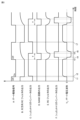
- 2 is a timing diagram showing the operation of the gate drive circuit of FIG. 1
- 11 is a schematic circuit diagram conceptually showing a charging state of a capacitor and a charging state of a gate capacitance immediately after a second electrode of the capacitor is connected to a reference potential.
- FIG. FIG. 13 is a diagram showing the change in the actual gate voltage over time after the driven element is turned off.
- 2 is a timing diagram showing the operation of the gate drive circuit of FIG. 1 when the on-pulse width of the gate drive signal is very short.
- 4 is a timing diagram showing the operation of a modified example of the gate drive circuit of FIG. 1.
- FIG. 1 is a circuit diagram showing a configuration example of a gate drive circuit according to a first embodiment
- 2 is a timing diagram showing the operation of the gate drive circuit of FIG. 1
- 11 is a schematic circuit diagram conceptually showing a charging state of a capacitor and
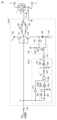
- FIG. 11 is a circuit diagram showing a configuration example of a gate drive circuit according to a second embodiment.
- FIG. 8 is a timing diagram showing the operation of the gate drive circuit of FIG. 7.
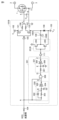
- FIG. 11 is a circuit diagram showing a configuration example of a gate drive circuit according to a third embodiment.
- FIG. 13 is a circuit diagram showing a configuration example of a gate drive circuit according to a fourth embodiment.
- Fig. 1 is a circuit diagram showing a configuration example of a gate drive circuit according to embodiment 1.
- a driven element 1 is a MOSFET.
- the driven element 1 has a drain terminal 2 as a first main terminal, a source terminal 3 as a second main terminal, and a gate terminal 4 as a control terminal.
- the main current flowing between the first and second main terminals is controlled to be turned on and off by the gate voltage applied to the gate terminal 4.
- the driven element 1 further has a source reference terminal 5 between the source electrode and the source terminal 3 to obtain the source potential.
- a parasitic gate capacitance 6 exists between the gate and source of the driven element 1.
- the gate capacitance does not exist as a component, but in Figure 1 it is virtually shown as if the component were connected by a dotted line.
- a gate drive circuit 101 is connected to a gate terminal 4 and a source terminal 3 of a driven element 1.
- the gate drive circuit 101 instead of the source terminal 3, is connected to a source reference terminal 5 provided between the source electrode of the driven element 1 and the source terminal 3.
- the gate drive circuit 101 has therein a power supply node 102 to which a positive potential V CC from a positive power supply is applied, and a reference node 103 to which a reference potential V SS is applied.
- the reference potential V SS is equal to the potential of the source reference terminal 5.
- the gate drive circuit 101 is driven by a gate drive signal GDS input to a signal input terminal 104.
- the gate drive circuit 101 has a mechanism for switching whether the gate terminal 4 of the driven element 1 is connected to the positive potential side or the reference potential side according to the input gate drive signal GDS.
- the gate drive circuit 101 includes a turn-on gate resistor 106 and a switch 121 (first switch) connected in series between the gate terminal 4 and the power supply node 102 to switch the gate terminal 4 to the positive potential side.
- the gate drive circuit 101 also includes a turn-off gate resistor 107 and a switch 122 (second switch) connected in series between the gate terminal 4 and the reference node 103 to connect the gate terminal 4 to the reference potential side.
- the switch 121 is a P-channel MOSFET
- the switch 122 is an N-channel MOSFET.
- the gate resistor 106 is connected closer to the gate terminal 4 than the switch 121, and the gate resistor 107 is connected closer to the gate terminal 4 than the switch 122.
- the gate drive circuit 101 includes a non-inverting buffer 105 for driving the gate terminal of the switch 121 and the gate terminal of the switch 122 in response to the gate drive signal GDS.
- the gate drive signal GDS input to the signal input terminal 104 is input to the non-inverting buffer 105.
- the gate drive circuit 101 includes a diode 108, a capacitor 109, a potential switching circuit 201, a non-inverting buffer 110, and a signal generating circuit 301 as a mechanism for inputting a negative potential to the gate terminal 4 of the driven element 1.
- Diode 108 is connected between switch 122 and reference node 103 so that the anode of diode 108 is on the switch 122 side and the cathode of diode 108 is on the reference node 103 side.
- the first electrode 109A of the capacitor 109 is connected to the connection point between the switch 122 and the diode 108.
- the second electrode 109B of the capacitor 109 is connected to the potential switching circuit 201.
- the potential switching circuit 201 has a pull-up resistor 202 and a switch 203 (third switch).
- the switch 203 is an N-channel MOSFET.
- a first end of the pull-up resistor 202 is connected to the power supply node 102, and a second end of the pull-up resistor 202 is connected to both the second electrode 109B of the capacitor 109 and the drain terminal of the switch 203.
- a source terminal of the switch 203 is connected to the reference node 103.
- a gate terminal of the switch 203 is driven by the non-inverting buffer 110.
- the signal generating circuit 301 receives as input the gate drive signal input to the signal input terminal 104, and outputs a control signal that drives the non-inverting buffer 110.
- a high-level control signal is output from the signal generating circuit 301 to the non-inverting buffer 110, the switch 203 turns on, thereby enabling the negative bias of the gate terminal 4 of the driven element 1.
- a low-level control signal is output from the signal generating circuit 301 to the non-inverting buffer 110, the switch 203 turns off, thereby disabling the negative bias of the gate terminal 4 of the driven element 1.
- the high-level control signal is also referred to as an enabled control signal
- the low-level control signal is also referred to as a disabled control signal.
- the signal generating circuit 301 includes a first delay circuit 320, a logical operation circuit 306, and a second delay circuit 321.
- the first delay circuit 320 receives a negative logic gate drive signal GDS.
- the first delay circuit 320 generates a first delay signal by delaying the turn-off edge (i.e., rising edge) of the input negative logic gate drive signal GDS without delaying the turn-on edge (i.e., falling edge). Furthermore, the first delay circuit 320 outputs a signal that inverts the logical value of the first delay signal.
- the first delay circuit 320 includes a low-pass filter (also called an RC filter) composed of a resistor 303 and a capacitor 304, a diode 302, and a Schmitt trigger inverter 305.
- the resistor 303 and the capacitor 304 are connected in series between the signal input terminal 104 and the reference node 103 in this order.
- the diode 302 is connected in parallel with the resistor 303.
- the anode terminal of the diode 302 is connected to a connection node B between the resistor 303 and the capacitor 304. This allows the RC filter to function as a one-way RC filter that delays only the rising edge of the gate drive signal GDS.
- the signal that passes through the RC filter is input to the Schmitt trigger inverter 305.
- the Schmitt trigger inverter 305 shapes the input signal and inverts its logical value.
- the logical operation circuit 306 calculates the logical AND of the inverted signal of the first delay signal output from the first delay circuit 320 and the gate drive signal GDS.
- a NAND (Not AND) circuit is used as the logical operation circuit 306, so the logical operation circuit 306 inverts and outputs the result of the logical AND.
- the logical operation circuit 306 may also calculate the logical OR of the first delay signal and the inverted signal of the gate drive signal GDS, and the logical operation result will be the same.
- the output signal of the logical operation circuit 306 is input to the second delay circuit 321.
- the second delay circuit 321 delays the output signal of the logical operation circuit 306 (i.e., both the rising edge and the falling edge).
- the delayed signal output from the second delay circuit 321 is input to the non-inverting buffer 110. This generates a control signal for controlling the potential switching circuit 201.
- the second delay circuit 321 includes a low-pass filter (also called an RC filter) composed of a resistor 307 and a capacitor 308, and a Schmitt trigger inverter 309.
- the resistor 307 and the capacitor 308 are connected in series, in this order, between the output node D of the logic operation circuit 306 and the reference node 103.
- the signal that has passed through the RC filter is input to the Schmitt trigger inverter 309.
- the Schmitt trigger inverter 309 shapes the input signal and inverts its logical value.
- Fig. 2 is a timing diagram showing the operation of the gate drive circuit 101 of Fig. 1.
- Fig. 2 shows the signal waveforms of nodes A to F of Fig. 1 and the waveform of the gate voltage VG of the driven element 1. Each will be described below in order.
- the signal at node A is a gate drive signal GDS, and is input to the gate terminal of switch 121 (a P-channel MOSFET) and the gate terminal of switch 122 (an N-channel MOSFET) via non-inverting buffer 105.
- Switches 121 and 122 form a complementary metal-oxide-semiconductor (CMOS).
- CMOS complementary metal-oxide-semiconductor
- the switch 122 When the gate drive signal GDS is at a high level, the switch 122 is turned on, connecting the gate terminal 4 of the driven element 1 to the reference node 103. This places the driven element 1 in an off state. On the other hand, when the gate drive signal GDS is at a low level, the switch 121 is turned on, connecting the gate terminal 4 of the driven element 1 to the power supply node 102. This places the driven element 1 in an on state. Therefore, the gate drive signal GDS is negative logic.
- Time t1 when the gate drive signal GDS switches from high to low corresponds to the turn-on edge.
- Time t3 when the gate drive signal GDS switches from low to high corresponds to the turn-off edge.
- the signal at node B represents the signal output from the one-way RC filter of the first delay circuit 320 when the signal at node A (i.e., the gate drive signal GDS) is input to the one-way RC filter.
- a low-pass filter made up of a resistor and a capacitor cuts out the high-frequency components of an input signal and passes the low-frequency components of the input signal.
- the signal that passes through the low-pass filter has a shape with blunted edges compared to the input signal.
- a diode 302 is connected in parallel with a resistor 303. The cathode of the diode 302 is connected to the input side of the low-pass filter, and the anode of the diode 302 is connected to the output side of the low-pass filter, so that when the input signal rises, the diode is in a cutoff state and the low-pass filter is active.
- the RC filter of the first delay circuit 320 functions as a one-way filter that is active only on the rising edge of the input signal.
- the output signal of the unidirectional RC filter i.e., the signal at node B
- time t3 which is the rising edge (i.e., the turn-off edge) of the gate drive signal GDS
- the output signal of the unidirectional RC filter rises slowly.
- the signal at node C represents the signal output from the Schmitt trigger inverter 305 when the signal at node B (i.e., the output signal of the one-way RC filter) is input to the Schmitt trigger inverter 305.
- a Schmitt trigger element is an element that has hysteresis in the input threshold voltage.
- the first delay circuit 320 uses a Schmitt trigger inverter 305, it outputs a signal that inverts the logical value of the input signal.
- Schmitt trigger inverter 305 when the input signal to Schmitt trigger inverter 305 (i.e., the signal at node B) falls at time t1 in FIG. 2, Schmitt trigger inverter 305 outputs a signal that is the inversion of the input signal after the input signal becomes significantly lower than the midpoint potential. Because the signal at node B falls abruptly at time t1, the output signal from Schmitt trigger inverter 305 rises at time t2 with almost no delay from time t1.
- the Schmitt trigger inverter 305 when the input signal of the Schmitt trigger inverter 305 (i.e., the signal at node B) rises at time t3, the Schmitt trigger inverter 305 outputs a signal that is an inversion of the input signal after the input signal becomes significantly higher than the midpoint potential. Since the signal at node B rises slowly at time t3, the output signal of the Schmitt trigger inverter 305 falls at time t5, which is significantly delayed from time t3.
- the Schmitt trigger inverter 305 When a signal waveform with only the rising edge delayed as described above is input to the Schmitt trigger inverter 305, the Schmitt trigger inverter 305 outputs an inverted signal with only the rising edge of the input signal significantly delayed.
- the signal at node D represents the output signal of the NAND circuit serving as the logical operation circuit 306.
- the NAND circuit 306 outputs a signal obtained by inverting the logical product of the signal at node A (i.e., the gate drive signal GDS) and the signal at node C (i.e., the output signal of the Schmitt trigger inverter 305).
- the logical product of the signal at node A and the signal at node C is true only for a certain period T from the turn-off edge (for example, from time t3 to time t5 in FIG. 2) and is false during other periods. Therefore, the signal at node D (i.e., the output signal of NAND circuit 306) is at the reference potential only for a certain period T from the turn-off edge and is at a positive potential during other periods.
- the signal at node E represents the signal output from an RC filter formed by resistor 307 and capacitor 308 when the signal at node D is input to this RC filter. Since no diode is connected to resistor 307 of this RC filter, the signal waveform at node D has dull rising and falling edges.
- the signal at node F represents the signal output from Schmitt trigger inverter 309 when the signal at node E (i.e., the output signal of the RC filter) is input to Schmitt trigger inverter 309.
- the signal at node F is a signal in which both the rising and falling edges of the signal at node D are delayed and then their logical values are inverted. Specifically, the signal at node F goes from low level to high level at time t4, a certain time after the turn-off edge at time t3, and then goes back from high level to low level at time t6.
- the signal generating circuit 301 inputs this signal of node F to the gate terminal of the switch 203 of the potential switching circuit 201 via the non-inverting buffer 110 as a control signal for enabling the negative bias. Therefore, the switch 203 is conductive during the period when the signal of node F is at a high level (from time t4 to t6) during the period when the gate drive signal GDS is at a high level (from time t3 to time t7). During other periods, the switch 203 is non-conductive.
- the first electrode 109A of the capacitor 109 is connected to the connection point between the off-drive switch 122 and the diode 108.
- the second electrode 109B of the capacitor 109 is connected to the power supply node 102 via the pull-up resistor 202, and is connected to the reference node 103 via the switch 203.
- the gate voltage waveform shown at the bottom of Figure 2 is obtained by the operation of the signal generation circuit 301 and potential switching circuit 201 described above.
- the switch 121 of the gate drive circuit 101 is conductive, so that a positive potential is applied to the gate terminal 4 of the driven element 1.
- the switch 121 of the gate drive circuit 101 becomes non-conductive and the switch 122 becomes conductive, so that the charge stored in the gate terminal 4 of the driven element 1 is discharged via the gate resistor, the switch 122, and the forward diode 108.
- the gate terminal 4 of the driven element 1 changes from a positive potential to the reference potential.
- the signal at the node F is at a low level, so the switch 203 of the potential switching circuit 201 is non-conductive. Therefore, the first electrode 109A of the capacitor 109 is maintained at the same potential as the reference potential VSS via the diode 108.
- FIG. 3 is a schematic circuit diagram conceptually showing the charging state of the capacitor 109 and the charging state of the gate capacitance 6 immediately after the second electrode 109B of the capacitor 109 is connected to a reference potential.
- Figure 3 (A) shows the charging state of the capacitor 109 and the gate capacitance 6 in the comparative example.
- the capacitor 109 for generating a negative bias is connected to the gate capacitance 6 of the driven element 1 immediately after the driven element 1 is turned off.
- the gate terminal 4 is disconnected from the power supply node 102 and the capacitor 109 for generating a negative bias is connected to the gate capacitance 6 at the same time.
- the gate capacitance CGS is equal to the capacitance C1 of the capacitor 109.
- both the gate capacitance 6 and the capacitor 109 are charged with the positive potential V CC .
- the charges of the gate capacitance 6 and the capacitor 109 are completely cancelled out by connecting the gate capacitance 6 and the capacitor 109.
- the gate potential after the negative bias generating capacitor 109 is connected is zero, that is, it is the same as the reference potential V SS , and it does not become negative.
- FIG. 3(B) shows the charging status of the capacitor 109 and the gate capacitance 6 in this embodiment. This embodiment can solve the shortcomings of the comparative example described above.
- the negative bias generating capacitor 109 is connected between the gate terminal 4 and the reference node 103, so that part of the negative charge stored in the first electrode 109A of the capacitor 109 transfers to the gate terminal 4, and the remaining negative charge remains in the first electrode 109A of the capacitor 109. Therefore, unlike the comparative example in FIG. 3(A), the negative charge in the first electrode 109A of the capacitor 109 is not offset by the positive charge in the gate terminal 4. As a result, there is no need to increase the capacitance C1 of the negative bias generating capacitor 109.
- the capacitance of the capacitor 109 for generating a negative bias can be made smaller than in the past.
- the gate capacitance of the driven element 1 is CGS
- the capacitance of the capacitor for generating a negative bias is C1
- the gate power supply voltage is VCC
- the turn-on threshold of the driven element 1 is VTH .
- the gate capacitance CGS is once discharged, and then the negative bias generating capacitor 109 is connected to the gate capacitance CGS .
- the charge Q1 stored in the negative bias generating capacitor 109 is proportionally divided between the capacitor 109 and the gate capacitance CGS .
- of the voltage of the capacitor 109 is equal to the absolute value
- This voltage acts as a negative bias.
- the peak of the surge voltage should be lowered by a negative bias so that it becomes equal to or lower than the gate threshold voltage VTH .
- the absolute value of the minimum voltage required as a negative bias is equal to the difference between the surge peak V SURGE of the gate voltage of the own arm when the opposing arm is turned on without applying a negative bias, and the gate threshold voltage VTH of the driven element.
- across the capacitor 109 needs to be equal to or greater than this difference, so V SURGE -V TH ⁇
- C1/(C1+C GS ) ⁇ V CC ...(6) holds true.
- the right-hand side of the above equation (7) is the lower limit of the capacitance C1 of the capacitor 109. It is sufficient to ensure that the capacitance C1 does not fall below this lower limit.
- This lower limit value of capacitance C1 cannot be achieved by the conventional technology, and can only be achieved by discharging the gate capacitance CGS once after the driven element 1 is turned off, and then connecting the negative bias generating capacitor 109 to the gate capacitance CGS , as in this embodiment.
- Figure 4 shows the actual change in gate voltage over time after the driven element is turned off.
- the thin solid line waveform in Figure 4 shows the change in gate voltage over time when no negative bias is used, i.e., when there is no capacitor 109 for generating the negative bias.
- the opposing arm is turned on at time t12 after a dead time.
- the gate voltage of the own arm rises and rises to the surge peak V SURGE .
- the surge peak V SURGE exceeds the gate threshold voltage V TH , so there is a risk of the element being destroyed by false firing.
- the negative bias generating capacitor 109 is connected to the gate capacitance CGS , thereby applying a negative bias to the gate terminal 4. In this case, it is important not to make the capacitance C1 of the capacitor 109 unnecessarily large.
- the gate voltage V G can be lowered to near the inversion voltage ⁇ V CC of the power supply voltage V CC of the gate drive circuit 101, as shown by the thick solid line in FIG. 4.
- a large negative bias is unnecessary. This is because the effect of preventing erroneous arcing remains unchanged even if the peak of the surge voltage is significantly lower than the gate threshold voltage V TH .
- unnecessarily increasing the capacitance C1 of the capacitor 109 also causes problems such as an increase in circuit size and an increase in cost.
- the driven element is a SiC-MOSFET (silicon carbide MOSFET)
- SiC-MOSFET silicon carbide MOSFET
- the capacitance C1 Although there is no operational limit on the upper limit of the capacitance C1, as mentioned above, if it is unnecessarily large, it will lead to an increase in the circuit size and cost, and will have a negative effect on the gate oxide film. A possible reason why the capacitance C1 must be increased to a certain extent is a decrease in the gate threshold voltage VTH .
- the gate threshold voltage VTH may decrease from the initial value due to various factors, in which case the capacitance C1 must be increased accordingly. However, even in the worst case, the gate threshold voltage VTH is a positive value and is greater than 0V.
- the dashed waveform in FIG. 4 shows the change over time of the gate voltage V G when the capacitance of the capacitor 109 for generating the negative bias is optimized.
- the negative bias is suppressed to a minimum, and the surge peak of the gate voltage of the own arm when the opposing arm is turned on does not exceed VTH .
- the gate voltage is temporarily set to 0 before a negative bias is applied, so the period during which the negative bias is applied is also minimized.
- applying a negative bias to the gate places stress on the gate oxide film, so it is better to keep not only the magnitude of the negative bias but also the period during which the negative bias is applied as short as possible.
- the period during which the negative bias is applied to the gate can be limited to a short period that includes the moment when the opposing arm is turned on.
- the duration for which the negative bias is applied can be controlled by adjusting the time constant of the low-pass filter for generating the first signal in FIG. 1, i.e., the size of resistor 303 and/or capacitor 304.
- the time position at which the negative bias begins to be applied can be controlled by adjusting the time constant of the low-pass filter that delays the first signal, i.e., the size of resistor 307 and/or capacitor 308. By controlling these, the application time of the negative bias can be kept to a necessary minimum. This is also an effect that could not be achieved with conventional technology.
- the first delay circuit 320 is configured as a one-way RC filter that delays only the turn-off edge of the gate drive signal GDS without delaying the turn-on edge. This ensures that a negative bias can be applied to the gate terminal 4 of the driven element 1 even if the on-pulse width of the gate drive signal GDS is very short. A specific example will be described below.
- Fig. 5 is a timing diagram showing the operation of the gate drive circuit 101 in Fig. 1 when the on-pulse width of the gate drive signal GDS is very short.
- the timing diagram in Fig. 5 corresponds to the timing diagram in Fig. 2, and shows the signal waveforms of nodes A to F in Fig. 1 and the waveform of the gate voltage VG of the driven element 1.
- Times t1 to t7 in Fig. 5 correspond to times t1 to t7 in Fig. 2, respectively.
- the on-pulse width (i.e., from time t1 to time t3) of the gate drive signal GDS (i.e., the signal at node A) is very short. Even in such a case, a negative bias can be applied to the gate terminal 4 between time t4 and time t6 after the turn-off edge at time t3.
- FIG. 6 is a timing diagram showing the operation of a modified gate drive circuit 101 of FIG. 1.
- the first delay circuit 320 of the signal generation circuit 301 of FIG. 1 is configured not to include the diode 302. Therefore, the modified first delay circuit is a bidirectional delay circuit that delays both the turn-on edge and the turn-off edge.
- FIG. 6 shows the signal waveforms at nodes A to F in FIG. 1 and the waveform of the gate voltage VG of the driven element 1 in the case of the above-mentioned change.
- the waveform of the gate drive signal GDS (signal at node A) is the same as in FIG. 5.
- the waveform of the signal at node B begins to slowly decrease at the turn-on edge of the gate drive signal GDS at time t1. However, because the on-pulse width of the gate drive signal GDS is very short, the signal at node B is immediately pulled back slowly toward its original high level at the turn-off edge at time t3.
- the signal at node B does not exceed the operating threshold of the Schmitt trigger inverter 305 in the first delay circuit 320, so the Schmitt trigger inverter 305 does not operate.
- the modified signal generating circuit cannot detect the turn-off edge of the gate drive signal GDS. Therefore, the signal at node C remains at low (L) level, and in response, the signals at nodes D and E remain at high (H) level, and as a result, the signal at node F remains at low (L) level.
- no negative bias is applied to gate terminal 4. This causes false firing.
- Embodiment 2 is a circuit diagram showing a configuration example of a gate drive circuit 101A according to embodiment 2.
- the gate drive circuit 101A in FIG. 7 is a modified example of the gate drive circuit 101 in FIG.
- the gate drive circuit 101A in FIG. 7 differs from the gate drive circuit 101 in FIG. 1 in that an NPN transistor 131 (first switch) is used instead of the switch 121 configured by a P-channel MOSFET, and a PNP transistor 132 (second switch) is used instead of the switch 122 configured by an N-channel MOSFET.
- NPN transistor 131 first switch
- PNP transistor 132 second switch
- the base terminals of the NPN transistor 131 and the PNP transistor 132 are connected to the signal input terminal 104.
- the connection point 133 between the NPN transistor 131 and the PNP transistor 132 is connected to the gate terminal 4 of the driven element 1 via the gate resistor 106 for turn-on and the forward diode, and is also connected to the gate terminal 4 of the driven element 1 via the gate resistor 107 for turn-off and the reverse diode.
- the above-mentioned NPN transistor 131 and PNP transistor 132 form an emitter follower circuit, in which the logical value of the input signal matches the logical value of the output signal.
- the CMOS circuit formed by the switches 121 and 122 in FIG. 1 the logical value of the input signal is inverted from the logical value of the output signal. Therefore, while the gate drive signal GDS is input in negative logic to the gate drive circuit 101 in FIG. 1, the gate drive signal GDS is input in positive logic to the gate drive circuit 101 in FIG. 7.
- the driven element 1 By making the gate drive signal GDS positive logic, even if the circuit that generates the gate drive signal GDS fails for some reason and the input signal to the gate drive circuit 101 remains at the reference potential for a long period of time, the driven element 1 will not be turned on for a long period of time. This has the advantage of making it less likely to cause a short circuit or other accident.
- the signal generating circuit 301 in FIG. 1 is changed to the signal generating circuit 301A in FIG. 7.
- the signal generating circuit 301A in FIG. 7 includes a first delay circuit 320A, a NOT circuit 311, a logical operation circuit 306, a second delay circuit 321, a diode 108, a capacitor 109, and a non-inverting buffer 110.
- the configurations and connections of the second delay circuit 321, the diode 108, the capacitor 109, and the non-inverting buffer 110 are similar to those of the signal generating circuit 301 in FIG. 1, and therefore the same or corresponding parts are designated by the same reference characters and will not be described repeatedly.
- the positive logic gate drive signal GDS is input to the first delay circuit 320A.
- the first delay circuit 320A generates a first delay signal by delaying the turn-off edge (i.e., falling edge) of the input positive logic gate drive signal GDS without delaying the turn-on edge (i.e., rising edge).
- the first delay circuit 320A outputs the generated first delay signal.
- the first delay circuit 320A includes a low-pass filter (also called an RC filter) composed of a resistor 303 and a capacitor 304, a diode 302, and a Schmitt trigger buffer 305A.
- the resistor 303 and the capacitor 304 are connected in series between the signal input terminal 104 and the reference node 103 in this order.
- the diode 302 is connected in parallel with the resistor 303 and in the opposite direction to that in FIG. 1. That is, the cathode terminal of the diode 302 is connected to the connection node B between the resistor 303 and the capacitor 304.
- the signal that passes through the RC filter is input to the Schmitt trigger buffer 305A.
- the Schmitt trigger buffer 305A shapes the input signal but does not invert its logical value.
- the logical operation circuit 306 calculates the logical AND between the first delay signal output from the first delay circuit 320 and the signal obtained by inverting the gate drive signal GDS using the NOT circuit 311.
- a NAND circuit is used as the logical operation circuit 306, so the logical operation circuit 306 inverts and outputs the result of the logical AND.
- the logical operation circuit 306 may also calculate the logical OR between the inverted signal of the first delay signal and the gate drive signal GDS, and the logical operation result will be the same.
- FIG. 7 The rest of the configuration in FIG. 7 is the same as in FIG. 1, so the same or corresponding parts are given the same reference symbols and will not be described repeatedly.
- Fig. 8 is a timing diagram showing the operation of the gate drive circuit 101A of Fig. 7.
- the timing diagram of Fig. 8 corresponds to the timing diagram of Fig. 2, and shows the signal waveforms of nodes A to F of Fig. 8 and the waveform of the gate voltage VG of the driven element 1. Below, the points that differ from Fig. 2 will be described.
- the signal at node A is the gate drive signal GDS, and is input to the base terminal of NPN transistor 131 and the base terminal of PNP transistor 132.
- the PNP transistor 132 When the gate drive signal GDS is at a low level, the PNP transistor 132 is turned on, connecting the gate terminal 4 of the driven element 1 to the reference node 103. This causes the driven element 1 to be in an off state. On the other hand, when the gate drive signal GDS is at a high level, the NPN transistor 131 is turned on, connecting the gate terminal 4 of the driven element 1 to the power supply node 102. This causes the driven element 1 to be in an on state.
- the gate drive signal GDS is positive logic.
- the time t1 when the gate drive signal GDS switches from low level to high level corresponds to the turn-on edge.
- the time t3 when the gate drive signal GDS switches from high level to low level corresponds to the turn-off edge.
- the signal at node B represents the signal output from the unidirectional RC filter of the first delay circuit 320A when the signal at node A (i.e., the gate drive signal GDS) is input to this unidirectional RC filter.
- the signal at node A i.e., the gate drive signal GDS
- the unidirectional RC filter of the first delay circuit 320A when the input signal rises, the diode is in a conducting state, and the low-pass filter is disabled. Conversely, when the input signal falls, the diode is in a blocking state, and the low-pass filter is enabled.
- the output signal of the unidirectional RC filter rises quickly.
- time t3 which is the falling edge (i.e., turn-off edge) of the gate drive signal GDS
- the output signal of the unidirectional RC filter falls slowly.
- the signal at node C indicates the signal that is output from Schmitt trigger buffer 305A when the signal at node B (i.e., the output signal of the one-way RC filter) is input to Schmitt trigger buffer 305A.
- Schmitt trigger buffer 305A When a signal with only the falling edge that is dulled, such as the signal at node B in FIG. 8, is input to Schmitt trigger buffer 305A, Schmitt trigger buffer 305A outputs a signal in which only the falling edge of the input signal is significantly delayed.
- the signal at node D represents the output signal of the NAND circuit serving as the logical operation circuit 306.
- the NAND circuit 306 outputs a signal obtained by inverting the logical product of the signal at node A (i.e., the gate drive signal GDS) inverted by the NOT circuit 311 and the signal at node C (i.e., the output signal of the Schmitt trigger buffer 305A).
- the logical product of the inverted signal of the signal at node A and the signal at node C is true only for a certain period T from the turn-off edge (for example, from time t3 to time t5 in FIG. 2), and is false during other periods. Therefore, the signal at node D (i.e., the output signal of NAND circuit 306) is at the reference potential only for a certain period T from the turn-off edge, and is at a positive potential during other periods. This signal at node D is the same as the signal in FIG. 2 in the case of embodiment 1.
- the signals at nodes E and F and the gate voltage waveform VG are similar to those in FIG. 2, and therefore will not be described again.
- Embodiment 3. 9 is a circuit diagram showing a configuration example of a gate drive circuit 101B according to the embodiment 3.
- the configuration of a potential switching circuit 201B is different from the configuration of the potential switching circuit 201 of FIG 1 .
- the potential switching circuit 201 in FIG. 1 is an open-drain type that uses a pull-up resistor 202 and a switch 203 configured with an N-channel MOSFET.
- the potential switching circuit 201B in FIG. 9 is configured with an emitter-follower circuit that uses an NPN transistor 204 (third switch) and a PNP transistor 205 (fourth switch).
- an inverting buffer 111 is provided instead of the non-inverting buffer 110 in FIG. 1.
- the NPN transistor 204 and the PNP transistor 205 are connected in series between the power supply node 102 and the reference node 103 in this order.
- the base terminals of the NPN transistor 204 and the PNP transistor 205 are output to the output terminal of the inverting buffer 111.
- the connection point of the NPN transistor 204 and the PNP transistor 205 is connected to the second electrode 109B of the capacitor 109.
- the PNP transistor 205 When the control signal output from the inverting buffer 111 is at a low level (enabled), the PNP transistor 205 is turned on and the NPN transistor 204 is turned off, so the negative bias is enabled. When the control signal output from the inverting buffer 111 is at a high level (disabled), the PNP transistor 205 is turned off and the NPN transistor 204 is turned on, so the negative bias is disabled and the capacitor 109 is charged.
- the gate drive circuit 101B of the third embodiment has the advantage of being able to reduce power consumption compared to the gate drive circuit 101 of the first embodiment.
- Fig. 10 is a circuit diagram showing a configuration example of a gate drive circuit 101C according to the embodiment 4.
- the configuration of a potential switching circuit 201C is different from both the configuration of the potential switching circuit 201 in Fig. 1 and the configuration of the potential switching circuit 201B in Fig. 9.
- the potential switching circuit 201 in FIG. 1 is an open-drain type that uses a pull-up resistor 202 and a switch 203 that is composed of an N-channel MOSFET.
- the potential switching circuit 201B in FIG. 9 is composed of an emitter-follower circuit that uses an NPN transistor 204 and a PNP transistor 205.
- the potential switching circuit 201C in FIG. 10 is composed of a CMOS push-pull circuit that uses a P-channel MOSFET 206 (third switch) and an N-channel MOSFET 207 (fourth switch).
- the CMOS push-pull circuit operates with negative logic, just like the open-drain circuit.
- the P-channel MOSFET 206 and the N-channel MOSFET 207 are connected in series between the power supply node 102 and the reference node 103 in this order.
- the connection point of the P-channel MOSFET 206 and the N-channel MOSFET 207 is connected to the second electrode 109B of the capacitor 109.
- the resistor 208 and the diode 210 are connected in parallel with each other.
- the cathode of the diode 210 is connected to the gate terminal of the P-channel MOSFET 206, and the anode of the diode 210 is connected to the output terminal of the non-inverting buffer 110.
- the resistor 209 and the diode 211 are connected in parallel with each other.
- the cathode of the diode 211 is connected to the output terminal of the non-inverting buffer 110, and the anode of the diode 211 is connected to the gate terminal of the N-channel MOSFET 207.
- the N-channel MOSFET 207 When the control signal output from the non-inverting buffer 110 is at a high level (enabled), the N-channel MOSFET 207 is turned on and the P-channel MOSFET 206 is turned off, so the negative bias is enabled.
- the control signal output from the non-inverting buffer 110 is at a low level (disabled)
- the N-channel MOSFET 207 is turned off and the P-channel MOSFET 206 is turned on, so the negative bias is disabled and the capacitor 109 is charged.
- FIG. 10 The rest of the configuration in FIG. 10 is the same as in FIG. 1, so the same or corresponding parts are given the same reference symbols and will not be described repeatedly.
- a negative bias sufficient to prevent erroneous firing can be applied to the gate of the driven element 1 using a capacitor with a minimum required capacity.
- the gate drive circuits 101, 101A, 101B, and 101C of the first to fourth embodiments do not require a negative power supply, do not require special processing of the gate drive signal, and do not require a separate signal to enable the negative bias.
- the gate drive circuits of the first to fourth embodiments can be installed by directly replacing a conventional simple gate drive circuit without a negative bias. This means that the gate drive circuits can be easily installed in an operating device, and thus a function to prevent erroneous firing can be easily added. Therefore, the gate drive circuits of the first to fourth embodiments have a remarkable feature of having a wide range of applications.
- the driven element 1 is not limited to a MOSFET and may be an IGBT.
- the drain terminal of the MOSFET is replaced with a collector terminal, and the source terminal of the MOSFET is replaced with an emitter terminal.
- the potential switching circuit 201 of the first and second embodiments may be an open-drain circuit or an open-collector circuit.
- the potential switching circuit 201B described in the third embodiment and the potential switching circuit 201C described in the fourth embodiment can be combined with an emitter-follower circuit composed of the NPN transistor 131 and the PNP transistor 132 described in the second embodiment.
Landscapes
- Engineering & Computer Science (AREA)
- Power Engineering (AREA)
- Power Conversion In General (AREA)
- Logic Circuits (AREA)
Priority Applications (4)
| Application Number | Priority Date | Filing Date | Title |
|---|---|---|---|
| PCT/JP2023/016266 WO2024224475A1 (ja) | 2023-04-25 | 2023-04-25 | ゲート駆動回路 |
| CN202380097094.6A CN120982005A (zh) | 2023-04-25 | 2023-04-25 | 栅极驱动电路 |
| JP2025516348A JPWO2024224475A1 (https=) | 2023-04-25 | 2023-04-25 | |
| DE112023006257.9T DE112023006257T5 (de) | 2023-04-25 | 2023-04-25 | Gate-Treiberschaltung |
Applications Claiming Priority (1)
| Application Number | Priority Date | Filing Date | Title |
|---|---|---|---|
| PCT/JP2023/016266 WO2024224475A1 (ja) | 2023-04-25 | 2023-04-25 | ゲート駆動回路 |
Publications (1)
| Publication Number | Publication Date |
|---|---|
| WO2024224475A1 true WO2024224475A1 (ja) | 2024-10-31 |
Family
ID=93256074
Family Applications (1)
| Application Number | Title | Priority Date | Filing Date |
|---|---|---|---|
| PCT/JP2023/016266 Ceased WO2024224475A1 (ja) | 2023-04-25 | 2023-04-25 | ゲート駆動回路 |
Country Status (4)
| Country | Link |
|---|---|
| JP (1) | JPWO2024224475A1 (https=) |
| CN (1) | CN120982005A (https=) |
| DE (1) | DE112023006257T5 (https=) |
| WO (1) | WO2024224475A1 (https=) |
Citations (5)
| Publication number | Priority date | Publication date | Assignee | Title |
|---|---|---|---|---|
| JP2004159424A (ja) * | 2002-11-06 | 2004-06-03 | Mitsubishi Electric Corp | インバータ |
| JP2011193705A (ja) * | 2010-03-17 | 2011-09-29 | Hitachi Appliances Inc | 電圧駆動型半導体素子のゲート駆動回路及び電力変換装置 |
| JP2014187479A (ja) * | 2013-03-22 | 2014-10-02 | Denso Corp | 駆動回路 |
| JP2022027042A (ja) * | 2020-07-31 | 2022-02-10 | 国立大学法人京都工芸繊維大学 | ゲート駆動回路および電源回路 |
| WO2022180924A1 (ja) * | 2021-02-26 | 2022-09-01 | パナソニックIpマネジメント株式会社 | スイッチング制御回路およびゲート駆動回路 |
Family Cites Families (1)
| Publication number | Priority date | Publication date | Assignee | Title |
|---|---|---|---|---|
| JP5561352B2 (ja) | 2012-02-22 | 2014-07-30 | 株式会社デンソー | 駆動回路 |
-
2023
- 2023-04-25 JP JP2025516348A patent/JPWO2024224475A1/ja active Pending
- 2023-04-25 WO PCT/JP2023/016266 patent/WO2024224475A1/ja not_active Ceased
- 2023-04-25 DE DE112023006257.9T patent/DE112023006257T5/de active Pending
- 2023-04-25 CN CN202380097094.6A patent/CN120982005A/zh active Pending
Patent Citations (5)
| Publication number | Priority date | Publication date | Assignee | Title |
|---|---|---|---|---|
| JP2004159424A (ja) * | 2002-11-06 | 2004-06-03 | Mitsubishi Electric Corp | インバータ |
| JP2011193705A (ja) * | 2010-03-17 | 2011-09-29 | Hitachi Appliances Inc | 電圧駆動型半導体素子のゲート駆動回路及び電力変換装置 |
| JP2014187479A (ja) * | 2013-03-22 | 2014-10-02 | Denso Corp | 駆動回路 |
| JP2022027042A (ja) * | 2020-07-31 | 2022-02-10 | 国立大学法人京都工芸繊維大学 | ゲート駆動回路および電源回路 |
| WO2022180924A1 (ja) * | 2021-02-26 | 2022-09-01 | パナソニックIpマネジメント株式会社 | スイッチング制御回路およびゲート駆動回路 |
Also Published As
| Publication number | Publication date |
|---|---|
| CN120982005A (zh) | 2025-11-18 |
| DE112023006257T5 (de) | 2026-03-26 |
| JPWO2024224475A1 (https=) | 2024-10-31 |
Similar Documents
| Publication | Publication Date | Title |
|---|---|---|
| US4695744A (en) | Level shift circuit including source follower output | |
| KR100965686B1 (ko) | 레벨 시프트 회로 및 전원 장치 | |
| KR950008422B1 (ko) | 집적회로 및 이 회로에 사용하기 적합한 제어수단 | |
| JP3152204B2 (ja) | スルーレート出力回路 | |
| US8710878B2 (en) | Output circuit | |
| US8040162B2 (en) | Switch matrix drive circuit for a power element | |
| JP4235561B2 (ja) | 半ブリッジ駆動回路とその駆動回路を備える電力変換システム | |
| JP2655096B2 (ja) | 出力バッファ回路 | |
| US4437024A (en) | Actively controlled input buffer | |
| US10483977B1 (en) | Level shifter | |
| US10666250B2 (en) | Drive device for semiconductor element | |
| CN114204926B (zh) | 半导体装置 | |
| JP2011077629A (ja) | 半導体回路 | |
| CN112019001A (zh) | 高侧晶体管的驱动电路、开关电路、dc/dc转换器的控制器 | |
| EP0279332A1 (en) | A logic circuit used in standard IC of CMOS logic level | |
| JP4157010B2 (ja) | 駆動回路及び半導体装置 | |
| CN107078733A (zh) | 驱动电路 | |
| JP4792636B2 (ja) | 誘導性負荷駆動回路 | |
| JP2023063081A (ja) | スイッチング回路、dc/dcコンバータおよびその制御回路 | |
| JP2004260730A (ja) | パルス発生回路及びそれを用いたハイサイドドライバ回路 | |
| US8044685B2 (en) | Floating driving circuit | |
| JPH0693615B2 (ja) | ドライバ回路 | |
| US7501874B2 (en) | Level shift circuit | |
| EP0292713A2 (en) | Low voltage swing CMOS receiver circuit | |
| JP7471057B2 (ja) | ゲート駆動回路 |
Legal Events
| Date | Code | Title | Description |
|---|---|---|---|
| 121 | Ep: the epo has been informed by wipo that ep was designated in this application |
Ref document number: 23935256 Country of ref document: EP Kind code of ref document: A1 |
|
| ENP | Entry into the national phase |
Ref document number: 2025516348 Country of ref document: JP Kind code of ref document: A |
|
| WWE | Wipo information: entry into national phase |
Ref document number: 2025516348 Country of ref document: JP |
|
| WWE | Wipo information: entry into national phase |
Ref document number: 112023006257 Country of ref document: DE |
|
| WWP | Wipo information: published in national office |
Ref document number: 112023006257 Country of ref document: DE |
|
| 122 | Ep: pct application non-entry in european phase |
Ref document number: 23935256 Country of ref document: EP Kind code of ref document: A1 |