WO2024219283A1 - 多層回路基板 - Google Patents
多層回路基板 Download PDFInfo
- Publication number
- WO2024219283A1 WO2024219283A1 PCT/JP2024/014334 JP2024014334W WO2024219283A1 WO 2024219283 A1 WO2024219283 A1 WO 2024219283A1 JP 2024014334 W JP2024014334 W JP 2024014334W WO 2024219283 A1 WO2024219283 A1 WO 2024219283A1
- Authority
- WO
- WIPO (PCT)
- Prior art keywords
- interlayer connection
- conductor
- layer
- connection conductor
- circuit board
- Prior art date
- Legal status (The legal status is an assumption and is not a legal conclusion. Google has not performed a legal analysis and makes no representation as to the accuracy of the status listed.)
- Ceased
Links
Images


Classifications
-
- H—ELECTRICITY
- H05—ELECTRIC TECHNIQUES NOT OTHERWISE PROVIDED FOR
- H05K—PRINTED CIRCUITS; CASINGS OR CONSTRUCTIONAL DETAILS OF ELECTRIC APPARATUS; MANUFACTURE OF ASSEMBLAGES OF ELECTRICAL COMPONENTS
- H05K3/00—Apparatus or processes for manufacturing printed circuits
- H05K3/46—Manufacturing multilayer circuits
- H05K3/4611—Manufacturing multilayer circuits by laminating two or more circuit boards
- H05K3/4626—Manufacturing multilayer circuits by laminating two or more circuit boards characterised by the insulating layers or materials
- H05K3/4632—Manufacturing multilayer circuits by laminating two or more circuit boards characterised by the insulating layers or materials laminating thermoplastic or uncured resin sheets comprising printed circuits without added adhesive materials between the sheets
-
- H—ELECTRICITY
- H05—ELECTRIC TECHNIQUES NOT OTHERWISE PROVIDED FOR
- H05K—PRINTED CIRCUITS; CASINGS OR CONSTRUCTIONAL DETAILS OF ELECTRIC APPARATUS; MANUFACTURE OF ASSEMBLAGES OF ELECTRICAL COMPONENTS
- H05K1/00—Printed circuits
- H05K1/02—Details
- H05K1/0296—Conductive pattern lay-out details not covered by sub groups H05K1/02 - H05K1/0295
- H05K1/0298—Multilayer circuits
-
- H—ELECTRICITY
- H05—ELECTRIC TECHNIQUES NOT OTHERWISE PROVIDED FOR
- H05K—PRINTED CIRCUITS; CASINGS OR CONSTRUCTIONAL DETAILS OF ELECTRIC APPARATUS; MANUFACTURE OF ASSEMBLAGES OF ELECTRICAL COMPONENTS
- H05K1/00—Printed circuits
- H05K1/02—Details
- H05K1/09—Use of materials for the conductive, e.g. metallic pattern
-
- H—ELECTRICITY
- H05—ELECTRIC TECHNIQUES NOT OTHERWISE PROVIDED FOR
- H05K—PRINTED CIRCUITS; CASINGS OR CONSTRUCTIONAL DETAILS OF ELECTRIC APPARATUS; MANUFACTURE OF ASSEMBLAGES OF ELECTRICAL COMPONENTS
- H05K1/00—Printed circuits
- H05K1/02—Details
- H05K1/11—Printed elements for providing electric connections to or between printed circuits
-
- H—ELECTRICITY
- H05—ELECTRIC TECHNIQUES NOT OTHERWISE PROVIDED FOR
- H05K—PRINTED CIRCUITS; CASINGS OR CONSTRUCTIONAL DETAILS OF ELECTRIC APPARATUS; MANUFACTURE OF ASSEMBLAGES OF ELECTRICAL COMPONENTS
- H05K3/00—Apparatus or processes for manufacturing printed circuits
- H05K3/46—Manufacturing multilayer circuits
- H05K3/4611—Manufacturing multilayer circuits by laminating two or more circuit boards
- H05K3/4614—Manufacturing multilayer circuits by laminating two or more circuit boards the electrical connections between the circuit boards being made during lamination
- H05K3/4617—Manufacturing multilayer circuits by laminating two or more circuit boards the electrical connections between the circuit boards being made during lamination characterized by laminating only or mainly similar single-sided circuit boards
-
- H—ELECTRICITY
- H05—ELECTRIC TECHNIQUES NOT OTHERWISE PROVIDED FOR
- H05K—PRINTED CIRCUITS; CASINGS OR CONSTRUCTIONAL DETAILS OF ELECTRIC APPARATUS; MANUFACTURE OF ASSEMBLAGES OF ELECTRICAL COMPONENTS
- H05K2201/00—Indexing scheme relating to printed circuits covered by H05K1/00
- H05K2201/09—Shape and layout
- H05K2201/09818—Shape or layout details not covered by a single group of H05K2201/09009 - H05K2201/09809
- H05K2201/09827—Tapered, e.g. tapered hole, via or groove
Definitions
- the present invention relates to a multilayer circuit board.
- Patent Document 1 discloses an antenna board that includes a dielectric substrate having a first main surface and a second main surface, and an antenna conductor formed on the first main surface. Patent Document 1 further describes that a connection conductor is formed on the second main surface of the dielectric substrate, and that the connector of the circuit board is connected to the connection conductor of the antenna substrate, thereby connecting the circuit board to the antenna substrate.
- the interlayer connection conductor connected to the connection conductor with the electronic components (hereinafter referred to as the mounting electrode) is required to have a small diameter and a narrow pitch.
- Patent Document 1 describes a method of forming an interlayer connection conductor by filling holes in a dielectric layer with a conductive paste and solidifying it.
- the smaller the diameter of the hole the more difficult it becomes to fill the conductive paste in the depth direction, so there is a risk that sufficient connection reliability between the interlayer connection conductor and the conductor layer cannot be obtained.
- the present invention has been made to solve the above problems, and aims to provide a multilayer circuit board that has excellent connection reliability between the interlayer connection conductors and the conductor layers, even when the interlayer connection conductors are arranged with a small diameter and narrow pitch on the mounting surface for electronic components.
- the present invention makes it possible to provide a multilayer circuit board that has excellent connection reliability between the interlayer connection conductors and the conductor layers, even when the interlayer connection conductors are arranged with small diameters and narrow pitches on the mounting surface for electronic components.
- FIG. 1 is a cross-sectional view showing a schematic example of a multilayer circuit board according to the present invention.
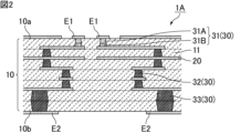
- FIG. 2 is a cross-sectional view showing a schematic example of a multilayer circuit board according to the first embodiment of the present invention.
- FIG. 3 is a cross-sectional view that illustrates an example of the first interlayer connection conductor 31.
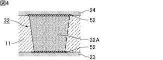
- FIG. 4 is a cross-sectional view that illustrates an example of the second interlayer connection conductor 32.
- FIG. 5 is a cross-sectional view that illustrates an example of the second interlayer connection conductor 33.
- FIG. 6A and 6B are cross-sectional views that typically show an example of a method for manufacturing the multilayer circuit board 1A.
- FIG. 6A and 6B are cross-sectional views that typically show an example of a method for manufacturing the multilayer circuit board 1A.
- FIG. 6A and 6B are cross-sectional views that typically show an example of a method for manufacturing the multilayer circuit board 1A.
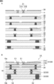
- FIG. 7 is a cross-sectional view showing a schematic example of a multilayer circuit board according to a second embodiment of the present invention.
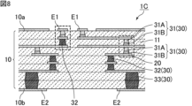
- FIG. 8 is a cross-sectional view showing a schematic example of a multilayer circuit board according to a third embodiment of the present invention.
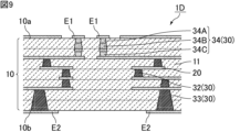
- FIG. 9 is a cross-sectional view showing a schematic example of a multilayer circuit board according to a fourth embodiment of the present invention.
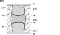
- FIG. 10 is a cross-sectional view that illustrates an example of the first interlayer connection conductor 34 .
- FIG. 11 is a cross-sectional view showing a schematic example of a multilayer circuit board according to a fifth embodiment of the present invention.
- FIG. 12 is a cross-sectional view illustrating an example of a multilayer circuit board according to a sixth embodiment of the present invention.
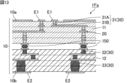
- FIG. 13 is a cross-sectional view showing a schematic diagram of another example of the multilayer circuit board according to the sixth embodiment of the present invention.
- FIG. 14 is a cross-sectional view illustrating an example of a multilayer circuit board according to a seventh embodiment of the present invention.
- FIG. 15 is a cross-sectional view showing a schematic example of a multilayer circuit board according to an eighth embodiment of the present invention.
- FIG. 16 is a cross-sectional view illustrating an example of a multilayer circuit board according to a ninth embodiment of the present invention.
- FIG. 17 is a cross-sectional view showing a schematic example of a multilayer circuit board according to a tenth embodiment of the present invention.
- the multilayer circuit board of the present invention will now be described.
- the present invention is not limited to the following configurations, and can be appropriately modified and applied within the scope of the present invention.
- the present invention also includes a combination of two or more of the individual preferred configurations of the present invention described below.
- terms indicating the relationship between elements are not expressions that only express a strict meaning, but are expressions that mean that they are substantially equivalent, for example, including differences of about a few percent.
- “equivalent” is an expression that does not only mean that they are completely equivalent, but is an expression that means that they are substantially equivalent, for example, including differences of about a few percent.
- FIG. 1 is a cross-sectional view showing a schematic example of a multilayer circuit board according to the present invention.
- the multilayer circuit board 1 shown in FIG. 1 comprises an insulating substrate 10, a plurality of conductor layers 20, and a plurality of interlayer connection conductors 30.
- the multilayer circuit board 1 may be a rigid board or a flexible board.
- the multilayer circuit board 1 may have a bent portion.
- the insulating substrate 10 is a laminate formed by stacking a plurality of insulating layers 11.
- the insulating substrate 10 has a first main surface 10a (upper surface in FIG. 1) and a second main surface 10b (lower surface in FIG. 1) that face each other in the stacking direction (vertical direction in FIG. 1).
- the conductor layer 20 is provided between the insulating layers 11 on the first principal surface 10a or the second principal surface 10b.
- a mounting electrode E1 is arranged as a conductor layer 20 on the first main surface 10a of the insulating substrate 10.
- a radiation electrode E2 is disposed as a conductor layer 20 on the second main surface 10b of the insulating substrate 10.
- the radiation electrode E2 may be any conductor layer of the conductor layer 20 that is disposed closest to the second main surface 10b, and does not necessarily have to be disposed on the second main surface 10b.
- the radiation electrode E2 constitutes the radiating element of the antenna.
- the operating frequency band of the radiating element is, for example, a high-frequency band such as the millimeter wave band.
- the interlayer connection conductors 30 are provided so as to penetrate the insulating layers 11 in the stacking direction.
- Each interlayer connection conductor 30 may be provided so as to penetrate one insulating layer 11 in the stacking direction, or may be provided so as to penetrate two or more insulating layers 11 in the stacking direction.
- Each interlayer connection conductor 30 is sandwiched between a conductor layer 20 on the first principal surface 10a side and a conductor layer 20 on the second principal surface 10b side in the stacking direction.
- An insulating protective layer 40 may be provided on the surface of the multilayer circuit board 1.
- the protective layer 40 may be, for example, a coverlay, a resist layer, or the like.
- the protective layer 40 may be provided on both of the first main surface 10a and the second main surface 10b, or on only one of the main surfaces.
- the multilayer circuit board 1 shown in FIG. 1 has electronic components 100 mounted thereon.
- the electronic components 100 are an integrated circuit (IC) 110, a high-frequency component 120, and a connector 130 mounted on the first main surface 10a of the multilayer circuit board 1.
- the integrated circuit 110 and the high-frequency component 120 are mounted on a dielectric substrate 140, and are mounted on the multilayer circuit board 1 via the dielectric substrate 140.
- the interlayer connection conductor 30 connected to the mounting electrode E1 is required to have a small diameter and a narrow pitch.
- the interlayer connection conductor 30 connected to the radiation electrode E2 does not need to be as small in diameter and have a narrower pitch as the interlayer connection conductor 30 connected to the mounting electrode E1.
- the connection strength can be increased by making the diameter of the interlayer connection conductor 30 connected to the radiation electrode E2 larger than the diameter of the interlayer connection conductor 30 connected to the mounting electrode E1.
- a first interlayer connection conductor or a second interlayer connection conductor described in each of the following embodiments is provided as the interlayer connection conductor 30.
- the conductor layer 20 that is connected to at least one first interlayer connection conductor is the mounting electrode E1. Also, the conductor layer 20 that is connected to at least one second interlayer connection conductor is the radiation electrode E2.
- FIG. 2 is a cross-sectional view showing a schematic example of a multilayer circuit board according to the first embodiment of the present invention.
- the multilayer circuit board 1A shown in FIG. 2 comprises an insulating substrate 10, a plurality of conductor layers 20, and a plurality of interlayer connection conductors 30.
- the insulating substrate 10 is a laminate formed by stacking a plurality of insulating layers 11.
- the insulating substrate 10 has a first main surface 10a (upper surface in FIG. 2) and a second main surface 10b (lower surface in FIG. 2) that face each other in the stacking direction (vertical direction in FIG. 2).
- the insulating layer 11 is, for example, a resin insulating layer whose main component is resin.
- the insulating layer 11 When the insulating layer 11 is a resin insulating layer, the insulating layer 11 may be a layer mainly composed of a thermosetting resin or a layer mainly composed of a thermoplastic resin, but preferably includes a layer mainly composed of a thermoplastic resin.
- the insulating layer 11 is made of a thermoplastic resin, multiple resin sheets on which the conductor layer 20 is formed can be stacked and collectively pressure-bonded (collectively pressed) by heat treatment.
- Thermosetting resins include epoxy resins, phenolic resins, polyimide resins or modified resins thereof, and acrylic resins.
- thermoplastic resins include liquid crystal polymers (LCPs), fluororesins, thermoplastic polyimide resins, polyether ether ketone resins (PEEK), polyphenylene sulfide resins (PPS), etc.
- LCPs liquid crystal polymers
- PEEK polyether ether ketone resins
- PPS polyphenylene sulfide resins
- the insulating layer 11 preferably includes a layer whose main component is a liquid crystal polymer. Liquid crystal polymers have a lower water absorption rate than other thermoplastic resins. Therefore, when the insulating layer 11 includes a layer whose main component is a liquid crystal polymer, the amount of moisture remaining in the insulating layer 11 can be reduced.
- the insulating layer 11 may contain an inorganic material such as a ceramic filler.
- Ceramic fillers include, for example, boron nitride, talc, and fused silica.
- each insulating layer 11 (length in the stacking direction) is preferably 10 ⁇ m or more and 100 ⁇ m or less.
- the thicknesses of each insulating layer 11 may be the same or different.
- the conductor layer 20 is provided between the insulating layers 11 on the first principal surface 10a or the second principal surface 10b.
- the conductor layer 20 may be in a patterned shape such as wiring, or may be in a planar shape that spreads over one surface.
- the shapes of the conductor layers 20 may be the same or different.
- each conductor layer 20 is made of Cu (copper) foil.
- the conductor layer 20 may have a matte surface on one main surface and a shiny surface on the other main surface.
- the thickness of the conductor layer 20 (length in the stacking direction) is preferably 1 ⁇ m or more and 35 ⁇ m or less, and more preferably 6 ⁇ m or more and 18 ⁇ m or less.
- the thicknesses of the conductor layers 20 may be the same as or different from each other.
- the conductor layers 20 may or may not be parallel to each other.
- a mounting electrode E1 is arranged as a conductor layer 20 on the first main surface 10a of the insulating substrate 10.
- a radiation electrode E2 is disposed as a conductor layer 20 on the second principal surface 10b of the insulating substrate 10.
- the radiation electrode E2 may be any conductor layer of the conductor layer 20 that is disposed closest to the second principal surface 10b, and does not necessarily have to be disposed on the second principal surface 10b.
- the interlayer connection conductor 30 includes a first interlayer connection conductor 31 and second interlayer connection conductors 32 and 33.
- the interlayer connection conductor 30 may include only one of the second interlayer connection conductors 32 and 33.
- the shape of the interlayer connection conductor 30 is preferably circular.
- circular shapes include not only perfect circles, but also ellipses, ovals, etc.
- the first interlayer connection conductor 31 includes a first portion 31A and a second portion 31B in the stacking direction.
- FIG. 3 is a cross-sectional view showing a schematic example of a first interlayer connection conductor 31.
- the top and bottom are reversed to those in FIG. 2.
- the first interlayer connection conductor 31 is sandwiched between the first conductor layer 21 and the second conductor layer 22 in the stacking direction.
- the first interlayer connection conductor 31 is provided so as to penetrate one insulating layer 11 in the stacking direction.
- the first portion 31A is made of a single metal whose main component is Cu.
- the first portion 31A is, for example, a plated via.
- a plated via means a film grown by a liquid phase method or a vapor phase method.
- the second portion 31B is made of an alloy material containing two or more kinds of metals, or a composite material containing one or more kinds of metals and a resin.
- the second portion 31B is made of an alloy containing two or more kinds of metals such as Ag, Cu, Ni, Sn, Cr, Pt, Mo, Ga, Ge, Sb, In, Pb, or the like, or is made of a composite material containing one or more kinds of metals such as Ag, Cu, Ni, Sn, Cr, Pt, Mo, Ga, Ge, Sb, In, Pb, or the like, and a resin.
- the alloy material include Cu-Sn alloys such as Cu 3 Sn and Cu 5 Sn, and Ag-Sn alloys such as Ag 3 Sn and Ag 5 Sn.
- the second portion 31B is, for example, a paste via.
- a paste via means a solidified paste.
- the second portion 31B functions as a bonding material, thereby electrically connecting the first portion 31A and the second conductor layer 22.
- One end of the first portion 31A is joined to the first conductor layer 21, and the other end of the first portion 31A is joined to one end of the second portion 31B.
- the first portion 31A and the first conductor layer 21 are directly bonded, without any dissimilar materials in between. Therefore, at the interface between the first portion 31A and the first conductor layer 21, there is a portion where no dissimilar materials are present, i.e., a portion where the first portion 31A and the first conductor layer 21 are in direct contact.
- an intermediate layer 51 containing Cu and the metal contained in the second portion 31B is formed at the end of the second portion 31B on the first portion 31A side.
- an intermediate layer 51 containing Cu and Sn is formed at the end of the second portion 31B on the first portion 31A side.
- the intermediate layer 51 is made of a Cu-Sn alloy such as Cu 3 Sn or Cu 5 Sn.
- the composition of the intermediate layer 51 is different from the composition of the second portion 31B.
- the other end of the second portion 31B is joined to the second conductor layer 22.
- an intermediate layer 51 containing Cu and the metal contained in the second portion 31B is formed in the second portion 31B at the end portion on the second conductor layer 22 side.
- an intermediate layer 51 containing Cu and Sn is formed in the second portion 31B at the end portion on the second conductor layer 22 side.
- the intermediate layer 51 is made of a Cu-Sn alloy such as Cu 3 Sn or Cu 5 Sn.
- the intermediate layer 51 can be confirmed, for example, by observing a cross section of the insulating layer 11 cut in a direction parallel to the stacking direction using a scanning electron microscope (SEM).
- SEM scanning electron microscope
- compositions such as Cu5Sn , Cu3Sn , and Cu6Sn5 all contain Cu and Sn as metal species, but the content ratios of the metal species are different, so they can be said to have different compositions.
- FIG. 4 is a cross-sectional view showing a schematic example of a second interlayer connection conductor 32. In FIG. 4, the top and bottom are reversed to FIG. 2.
- the second interlayer connection conductor 32 is sandwiched between the third conductor layer 23 and the fourth conductor layer 24 in the stacking direction.
- the second interlayer connection conductor 32 is provided so as to penetrate one insulating layer 11 in the stacking direction.
- the second interlayer connection conductor 32 includes a third portion 32A.
- the third portion 32A is made of an alloy material containing two or more kinds of metals, or a composite material containing one or more kinds of metals and a resin.
- the third portion 32A is made of an alloy containing two or more kinds of metals such as Ag, Cu, Ni, Sn, Cr, Pt, Mo, Ga, Ge, Sb, In, Pb, etc., or is made of a composite material containing one or more kinds of metals such as Ag, Cu, Ni, Sn, Cr, Pt, Mo, Ga, Ge, Sb, In, Pb, etc., and a resin.
- the alloy material include Cu-Sn alloys such as Cu 3 Sn and Cu 5 Sn, and Ag-Sn alloys such as Ag 3 Sn and Ag 5 Sn.
- the third portion 32A is, for example, a paste via.
- One end of the third portion 32A is joined to the third conductor layer 23, and the other end of the third portion 32A is joined to the fourth conductor layer 24.
- an intermediate layer 52 containing Cu and the metal contained in the third portion 32A is formed at an end portion on the third conductor layer 23 side and an end portion on the fourth conductor layer 24 side in the third portion 32A.
- an intermediate layer 52 containing Cu and Sn is formed at an end portion on the third conductor layer 23 side and an end portion on the fourth conductor layer 24 side in the third portion 32A.
- the intermediate layer 52 is made of a Cu-Sn alloy such as Cu 3 Sn or Cu 5 Sn.
- the composition of the intermediate layer 52 is different from the composition of the third portion 32A.
- FIG. 5 is a cross-sectional view showing a schematic example of a second interlayer connection conductor 33. In FIG. 5, the top and bottom are reversed to FIG. 2.
- the second interlayer connection conductor 33 is sandwiched between the third conductor layer 23 and the fourth conductor layer 24 in the stacking direction.
- the second interlayer connection conductor 33 is provided penetrating two insulating layers 11 in the stacking direction.
- the second interlayer connection conductor 33 has a shape in which a pair of second interlayer connection conductors 32 are connected in an inverted state.
- the third portion 33A is made of an alloy material containing two or more kinds of metals, or a composite material containing one or more kinds of metals and a resin.
- the third portion 33A is made of an alloy containing two or more kinds of metals such as Ag, Cu, Ni, Sn, Cr, Pt, Mo, Ga, Ge, Sb, In, Pb, etc., or is made of a composite material containing one or more kinds of metals such as Ag, Cu, Ni, Sn, Cr, Pt, Mo, Ga, Ge, Sb, In, Pb, etc., and a resin.
- the alloy material include Cu-Sn alloys such as Cu 3 Sn and Cu 5 Sn, and Ag-Sn alloys such as Ag 3 Sn and Ag 5 Sn.
- the third portion 33A is, for example, a paste via.
- One end of the third portion 33A is joined to the third conductor layer 23, and the other end of the third portion 33A is joined to the fourth conductor layer 24.
- an intermediate layer 52 containing Cu and the metal contained in the third portion 33A is formed at the end portion on the third conductor layer 23 side and the end portion on the fourth conductor layer 24 side of the third portion 33A.
- an intermediate layer 53 containing Cu and Sn is formed at the end portion on the third conductor layer 23 side and the end portion on the fourth conductor layer 24 side of the third portion 33A.
- the intermediate layer 53 is made of a Cu-Sn alloy such as Cu 3 Sn or Cu 5 Sn.
- the composition of the intermediate layer 53 is different from the composition of the third portion 33A.
- the multilayer circuit board 1A is characterized in that the first conductor layer 21 or the second conductor layer 22 connected to at least one first interlayer connection conductor 31 is a mounting electrode E1.
- the interlayer connection conductor 30 connected to the mounting electrode E1 is required to have a small diameter and a narrow pitch.
- first interlayer connection conductor 31 to the mounting electrode E1, the first interlayer connection conductor 31 including a first portion 31A such as a plated via that can reliably fill a hole even if the diameter is small, and a second portion 31B such as a paste via for complementing the connection with the adjacent layer.
- the first conductor layer 21 connected to the first interlayer connection conductor 31 may be the mounting electrode E1
- the second conductor layer 22 connected to the first interlayer connection conductor 31 may be the mounting electrode E1
- the first conductor layer 21 connected to the first interlayer connection conductor 31 is the mounting electrode E1. That is, as shown in FIG. 2, it is preferable that one end of the first portion 31A is joined to the mounting electrode E1.
- the multilayer circuit board 1A is characterized in that the third conductor layer 23 or the fourth conductor layer 24 connected to at least one second interlayer connection conductor 32 or 33 is a radiation electrode E2.
- the interlayer connection conductor 30 connected to the radiation electrode E2 does not need to be as small in diameter and narrow in pitch as the interlayer connection conductor 30 connected to the mounting electrode E1. Therefore, the interlayer connection conductor 30 joined to the radiation electrode E2 may be a second interlayer connection conductor 32 or 33 such as a paste via. Unlike the first interlayer connection conductor 31, no additional process such as plating is required, improving manufacturing efficiency.
- the second interlayer connection conductor 33 is connected to the radiation electrode E2, but the second interlayer connection conductor 32 may be connected to the radiation electrode E2.
- the radiation electrode E2 connected to the second interlayer connection conductor 32 and the radiation electrode E2 connected to the second interlayer connection conductor 33 may be mixed.
- the insulating layer 11 on which the first interlayer connection conductor 31 is provided and the insulating layer 11 on which the second interlayer connection conductor 32 or 33 is provided are both resin insulating layers whose main component is resin.
- the insulating layer 11 on which the first interlayer connection conductor 31 is provided and the insulating layer 11 on which the second interlayer connection conductor 32 or 33 is provided may each be a resin insulating layer whose main component is the same resin, or may be a resin insulating layer whose main component is a different resin.
- the shape, arrangement, etc. of the first interlayer connection conductor 31 are not limited to those shown in FIG. 2 or FIG. 3.
- the interlayer connection conductor 30 may include a first interlayer connection conductor 31 in which the first conductor layer 21 or the second conductor layer 22 is not a mounting electrode E1.
- the first interlayer connection conductor 31 may be provided in the insulating layer 11 located in the outermost layer on the first main surface 10a side, in the insulating layer 11 located in an inner layer, or in the insulating layer 11 located in the outermost layer on the second main surface 10b side.
- the first interlayer connection conductor 31 and the second interlayer connection conductor 32 or 33 may be mixed and provided in the insulating layer 11 of the same layer.
- the first interlayer connection conductor 31 may have a tapered shape in which the area of the end on the first conductor layer 21 side is smaller than the area of the end on the second conductor layer 22 side (see FIG. 3), or it may not have a tapered shape. If the first interlayer connection conductor 31 has a tapered shape, the inclination angle may be constant (see FIG. 3), or it may not be constant.
- the end face of the first portion 31A facing the second conductor layer 22 may be flat (see FIG. 2), may protrude toward the second portion 31B (see FIG. 3), or may be recessed toward the first portion 31A (not shown).
- the intermediate layer 51 When the intermediate layer 51 is formed at the end of the second portion 31B on the first portion 31A side, the intermediate layer 51 may extend to the interface between the first portion 31A and the insulating layer 11 (see FIG. 3), or may not extend to that interface.
- the intermediate layer 51 formed at the end of the second portion 31B on the first portion 31A side extends to the interface between the first portion 31A and the insulating layer 11, it may not reach the interface between the first conductor layer 21 and the insulating layer 11 (see FIG. 3), or may reach that interface.
- the intermediate layer 51 may extend to the interface between the second conductor layer 22 and the insulating layer 11 (see FIG. 3), or may not extend to the interface.
- the shape, arrangement, etc. of the second interlayer connection conductor 32 are not limited to those shown in FIG. 2 or FIG. 4.
- the interlayer connection conductor 30 may include a second interlayer connection conductor 32 in which the third conductor layer 23 or the fourth conductor layer 24 is not the radiation electrode E2.
- the second interlayer connection conductor 32 may be provided in the insulating layer 11 located in the outermost layer on the first principal surface 10a side, in the insulating layer 11 located in an inner layer, or in the insulating layer 11 located in the outermost layer on the second principal surface 10b side.
- the second interlayer connection conductor 32 and the second interlayer connection conductor 33 may be provided in a mixed state in the insulating layer 11 of the same layer.
- the second interlayer connection conductor 32 may have a tapered shape in which the end of the end face on the third conductor layer 23 side is smaller than the area of the end on the fourth conductor layer 24 side (see FIG. 4), or it may not have a tapered shape. If the second interlayer connection conductor 32 has a tapered shape, the inclination angle may be constant (see FIG. 4), or it may not be constant.
- the intermediate layer 52 When an intermediate layer 52 is formed on the end of the third portion 32A on the third conductor layer 23 side, the intermediate layer 52 may extend to the interface between the third conductor layer 23 and the insulating layer 11 (see FIG. 4), or may not extend thereto. Similarly, when an intermediate layer 52 is formed on the end of the third portion 32A on the fourth conductor layer 24 side, the intermediate layer 52 may extend to the interface between the fourth conductor layer 24 and the insulating layer 11 (see FIG. 4), or may not extend thereto.
- the height of the second interlayer connection conductor 32 is greater than the height of the first interlayer connection conductor 31.
- the diameter of the second interlayer connection conductor 32 is preferably equal to or greater than the diameter of the first interlayer connection conductor 31. That is, the diameter of the second interlayer connection conductor 32 is preferably equal to or greater than the diameter of the first interlayer connection conductor 31. Note that if the first interlayer connection conductor 31 has a tapered shape, the diameter of the largest part is defined as the diameter of the first interlayer connection conductor 31. The same applies to the second interlayer connection conductor 32 and the second interlayer connection conductor 33.
- the shape, arrangement, etc. of the second interlayer connection conductor 33 are not limited to those shown in FIG. 2 or FIG. 5.
- the interlayer connection conductor 30 may include a second interlayer connection conductor 33 in which the third conductor layer 23 or the fourth conductor layer 24 is not the radiation electrode E2.
- the second interlayer connection conductor 33 may be provided in the insulating layer 11 located in the outermost layer on the first principal surface 10a side, in the insulating layer 11 located in an inner layer, or in the insulating layer 11 located in the outermost layer on the second principal surface 10b side.
- the second interlayer connection conductor 32 and the second interlayer connection conductor 33 may be provided in a mixed state in the insulating layer 11 of the same layer.
- the second interlayer connection conductor 33 may have a shape in which a set of second interlayer connection conductors 32 having a tapered shape are connected in an inverted state (see FIG. 5), or may not have a tapered shape.
- the intermediate layer 53 When an intermediate layer 53 is formed on the end of the third portion 33A on the third conductor layer 23 side, the intermediate layer 53 may extend to the interface between the third conductor layer 23 and the insulating layer 11 (see FIG. 5), or may not extend thereto. Similarly, when an intermediate layer 53 is formed on the end of the third portion 33A on the fourth conductor layer 24 side, the intermediate layer 53 may extend to the interface between the fourth conductor layer 24 and the insulating layer 11 (see FIG. 5), or may not extend thereto.
- the height of the second interlayer connection conductor 33 is preferably greater than the height of the first interlayer connection conductor 31. Also, the height of the second interlayer connection conductor 33 is preferably greater than the height of the second interlayer connection conductor 32.
- the diameter of the second interlayer connection conductor 33 is preferably equal to or greater than the diameter of the first interlayer connection conductor 31. That is, the diameter of the second interlayer connection conductor 33 is preferably equal to or greater than the diameter of the first interlayer connection conductor 31. Also, the diameter of the second interlayer connection conductor 33 is preferably equal to or greater than the diameter of the second interlayer connection conductor 32. That is, the diameter of the second interlayer connection conductor 33 is preferably equal to or greater than the diameter of the second interlayer connection conductor 32.
- the multilayer circuit board 1A is manufactured, for example, by the following method.
- FIGS. 6A and 6B are cross-sectional views that show a schematic example of a method for manufacturing a multilayer circuit board 1A.
- the multilayer circuit board 1A may be manufactured in a one-chip (individual piece) state, or may be manufactured by producing an aggregate board and then separating it into individual pieces.
- the aggregate board here refers to a board that includes multiple multilayer circuit boards 1A.
- each insulating layer 11 is prepared, and a conductor layer 20 is formed on each insulating layer 11.
- the insulating layer 11 is, for example, a resin sheet whose main component is a thermoplastic resin such as a liquid crystal polymer.
- first interlayer connection conductor 31 and a second interlayer connection conductor 32 are formed on the insulating layer 11.
- a through hole (also called a via hole) is formed in the insulating layer 11 using a laser or the like so that one side of the conductor layer 20 is exposed.
- the through hole may have a tapered shape in which the hole diameter decreases toward the conductor layer 20.
- a plating process is performed to fill the through hole partway with Cu as a metal material, thereby forming the first portion 31A.
- a conductive paste containing a metal material such as Cu or Sn and a resin material is filled inside the through hole to form the second portion 31B.
- the conductive paste is solidified by a heating press described below, thereby forming the first interlayer connection conductor 31.
- a through hole is formed in the insulating layer 11 by a laser or the like so that one side of the conductor layer 20 is exposed, and then a conductive paste containing a metal material such as Cu or Sn and a resin material is filled into the through hole to form the third portion 32A.
- the conductive paste is solidified by a heating press, which will be described later, to form the second interlayer connection conductor 32.
- the second interlayer connection conductor 33 (see FIG. 6B) is formed in the portion where the two third portions 32A are connected in an inverted state.
- Each insulating layer 11 is stacked in order, and then hot pressed (collectively pressed) in the stacking direction. This produces the multilayer circuit board 1A shown in Figure 6B.
- the insulating layer 11 can be pressed together to easily produce the insulating base material 10. This reduces the number of manufacturing steps for the multilayer circuit board 1A, and keeps manufacturing costs low.
- an anti-rust layer may be provided on the surface of the conductor layer 20. This also applies to the following embodiments.
- the anti-rust layer is formed by applying an anti-rust treatment to the surface of the metal foil using metals such as Zn, Ni, Cr, Mo, and Pt.
- the multilayer circuit board 1A is produced by the batch pressing described above, by disposing an anti-rust layer at the interface between the conductor layer 20 and the insulating layer 11, oxidation of the metal foil such as Cu foil that constitutes the conductor layer 20 is prevented, and therefore a decrease in adhesion between the conductor layer 20 and the insulating layer 11 can be suppressed.
- a first interlayer connection conductor is provided in an insulating layer located in an inner layer.
- FIG. 7 is a cross-sectional view showing a schematic example of a multilayer circuit board according to a second embodiment of the present invention.
- the first interlayer connection conductor 31 is provided not only in the insulating layer 11 located on the outermost layer on the first main surface 10a side, but also in the insulating layer 11 located in the inner layer. Note that the first interlayer connection conductor 31 and the second interlayer connection conductor 32 or 33 may be provided together in the insulating layer 11 of the same layer.
- the first interlayer connection conductor may be provided on each of the insulating layers adjacent in the stacking direction. This allows wiring to be routed to the inner layer via the small-diameter interlayer connection conductor, which reduces the parasitic capacitance of the high-frequency circuit connecting, for example, the integrated circuit to the antenna, and improves characteristics.
- the interlayer connection conductors as the ground conductors around the signal line with a small diameter and narrow pitch, it is possible to prevent electric field leakage even at high frequencies of, for example, several tens of GHz.
- the first interlayer connection conductor overlaps at least a part of the first or second interlayer connection conductor adjacent to it in the stacking direction.
- FIG. 8 is a cross-sectional view showing a schematic example of a multilayer circuit board according to a third embodiment of the present invention.
- the first interlayer connection conductor 31 provided on the first insulating layer 11 from the top overlaps at least a portion of the second interlayer connection conductor 32 provided on the second insulating layer 11.
- the central axis of the first interlayer connection conductor 31 provided on the first insulating layer 11 coincides with the central axis of the second interlayer connection conductor 32 provided on the second insulating layer 11, but they do not have to coincide.
- the first interlayer connection conductor 31 provided in the second insulating layer 11 from the top overlaps at least a portion of the first interlayer connection conductor 31 provided in the third insulating layer 11.
- the central axis of the first interlayer connection conductor 31 provided in the second insulating layer 11 coincides with the central axis of the first interlayer connection conductor 31 provided in the third insulating layer 11, but they do not have to coincide.
- two interlayer connection conductors including the first interlayer connection conductor are overlapped, but three or more interlayer connection conductors including the first interlayer connection conductor may be overlapped.
- the first interlayer connection conductor, the second interlayer connection conductor, and the first interlayer connection conductor may be overlapped in this order.
- the second interlayer connection conductor may overlap at least a portion of the first or second interlayer connection conductor adjacent to it in the stacking direction.
- two interlayer connection conductors including the second interlayer connection conductor may overlap, or three or more interlayer connection conductors including the second interlayer connection conductor may overlap.
- the first interlayer connection conductor further includes a fourth portion, and is provided so as to penetrate two insulating layers in the stacking direction.
- FIG. 9 is a cross-sectional view showing a schematic example of a multilayer circuit board according to a fourth embodiment of the present invention.
- the interlayer connection conductor 30 includes a first interlayer connection conductor 34 and second interlayer connection conductors 32 and 33.
- the interlayer connection conductor 30 may include only one of the second interlayer connection conductors 32 and 33.
- the interlayer connection conductor 30 may further include a first interlayer connection conductor 31 (see FIG. 2).
- the first interlayer connection conductor 34 includes a first portion 34A, a second portion 34B, and a fourth portion 34C in the stacking direction.
- FIG. 10 is a cross-sectional view showing a schematic example of a first interlayer connection conductor 34. In FIG. 10, the top and bottom are reversed to FIG. 9.
- the first interlayer connection conductor 34 is sandwiched between the first conductor layer 21 and the second conductor layer 22 in the stacking direction.
- the first interlayer connection conductor 34 is provided to penetrate the two insulating layers 11 in the stacking direction.
- the first interlayer connection conductor 34 has a shape in which a pair of first interlayer connection conductors 31 are connected in an inverted state.
- the first portion 34A is made of a single metal whose main component is Cu.
- the first portion 34A is, for example, a plated via.
- the second portion 34B is made of an alloy material containing two or more kinds of metals, or a composite material containing one or more kinds of metals and a resin.
- the second portion 34B is made of an alloy containing two or more kinds of metals such as Ag, Cu, Ni, Sn, Cr, Pt, Mo, Ga, Ge, Sb, In, Pb, etc., or is made of a composite material containing one or more kinds of metals such as Ag, Cu, Ni, Sn, Cr, Pt, Mo, Ga, Ge, Sb, In, Pb, etc., and a resin.
- Specific examples of the alloy material include Cu-Sn alloys such as Cu 3 Sn and Cu 5 Sn, and Ag-Sn alloys such as Ag 3 Sn and Ag 5 Sn.
- the second portion 34B is, for example, a paste via.
- the fourth portion 34C is made of a single metal whose main component is Cu.
- the fourth portion 34C is, for example, a plated via.
- One end of the first portion 34A is joined to the first conductor layer 21, and the other end of the first portion 34A is joined to one end of the second portion 34B.
- the first portion 34A and the first conductor layer 21 are directly bonded, without any dissimilar materials in between. Therefore, at the interface between the first portion 34A and the first conductor layer 21, there is a portion where no dissimilar materials exist, i.e., a portion where the first portion 34A and the first conductor layer 21 are in direct contact.
- an intermediate layer 54 containing Cu and the metal contained in the second portion 34B is formed at the end of the second portion 34B on the first portion 34A side.
- an intermediate layer 54 containing Cu and Sn is formed at the end of the second portion 34B on the first portion 34A side.
- the intermediate layer 54 is made of a Cu-Sn alloy such as Cu 3 Sn or Cu 5 Sn.
- the composition of the intermediate layer 54 is different from the composition of the second portion 34B.
- One end of the fourth portion 34C is joined to the other end of the second portion 34B, and the other end of the fourth portion 34C is joined to the second conductor layer 22.
- the fourth portion 34C and the second conductor layer 22 are directly bonded, without any dissimilar materials in between. Therefore, at the interface between the fourth portion 34C and the second conductor layer 22, there is a portion where no dissimilar materials are present, i.e., a portion where the fourth portion 34C and the second conductor layer 22 are in direct contact.
- an intermediate layer 54 containing Cu and the metal contained in the second portion 34B is formed at the end of the second portion 34B on the fourth portion 34C side.
- an intermediate layer 54 containing Cu and Sn is formed at the end of the second portion 34B on the fourth portion 34C side.
- the intermediate layer 54 is made of a Cu-Sn alloy such as Cu 3 Sn or Cu 5 Sn.
- the composition of the intermediate layer 54 is different from the composition of the second portion 34B.
- the degree of freedom for routing the wiring is increased compared to the first interlayer connection conductor 31, so more space can be secured for the circuit. As a result, high-density wiring of the inner layers is possible.
- the shape, arrangement, etc. of the first interlayer connection conductor 34 are not limited to those shown in FIG. 9 or FIG. 10.
- the interlayer connection conductor 30 may include a first interlayer connection conductor 34 in which the first conductor layer 21 or the second conductor layer 22 is not a mounting electrode E1.
- the first interlayer connection conductor 34 may be provided in the insulating layer 11 located in the outermost layer on the first main surface 10a side, in the insulating layer 11 located in an inner layer, or in the insulating layer 11 located in the outermost layer on the second main surface 10b side.
- the multilayer circuit board 1D may include a mixture of the first interlayer connection conductor 31 and the first interlayer connection conductor 34.
- the first interlayer connection conductor 34 may have a shape in which a set of first interlayer connection conductors 31 having a tapered shape are connected in an inverted state (see FIG. 10), or may not have a tapered shape.
- the height of the first interlayer connection conductor 34 is preferably greater than the height of the first interlayer connection conductor 31.
- the height of the first interlayer connection conductor 34 may be equal to the height of the second interlayer connection conductor 32 or 33, may be greater than the height of the second interlayer connection conductor 32 or 33, or may be smaller than the height of the second interlayer connection conductor 32 or 33.
- the diameter of the first interlayer connection conductor 34 is preferably equal to the diameter of the first interlayer connection conductor 31. Also, the diameter of the first interlayer connection conductor 34 is preferably equal to or smaller than the diameter of the second interlayer connection conductor 32 or 33. In other words, the diameter of the first interlayer connection conductor 34 is preferably equal to or smaller than the diameter of the second interlayer connection conductor 32 or 33.
- a recess is provided in the second main surface of the insulating base material, and the insulating base material is bent toward the first main surface at the recess.
- FIG. 11 is a cross-sectional view showing a schematic example of a multilayer circuit board according to a fifth embodiment of the present invention.
- a recess 10M is provided on the second main surface 10b of the insulating substrate 10, and the insulating substrate 10 is folded toward the first main surface 10a at the recess 10M.
- the depth and folding angle of the recess 10M There are no particular limitations on the depth and folding angle of the recess 10M.
- multiple recesses 10M may be provided.
- the insulating substrate becomes easier to bend. This makes it possible to change the direction of the antenna surface for different frequencies or bands, for example, and thus give a single multilayer circuit board multiple antenna directivities.
- a material constituting an insulating layer on which a second interlayer connection conductor connected to a radiation electrode is provided is different from a material constituting an insulating layer on which a first interlayer connection conductor connected to a mounting electrode is provided.
- the dielectric constant of the insulating layer on which the second interlayer connection conductor connected to a radiation electrode is provided is higher than the dielectric constant of the insulating layer on which the first interlayer connection conductor connected to a mounting electrode is provided.
- FIG. 12 is a cross-sectional view showing a schematic example of a multilayer circuit board according to a sixth embodiment of the present invention.
- the insulating substrate 10 includes an insulating layer 11 and an insulating layer 12 made of a material different from that of the insulating layer 11.
- the insulating substrate 10 includes an insulating layer 11 and an insulating layer 12 having a higher dielectric constant than the insulating layer 11.
- the insulating layer 11 is provided with the first interlayer connection conductor 31, and the insulating layer 12 is provided with the second interlayer connection conductor 32 or 33, but the boundary between the insulating layer 11 and the insulating layer 12 is not particularly limited, and the material constituting the insulating layer 12 in which the second interlayer connection conductor (second interlayer connection conductor 33 in FIG. 12) connecting with the radiation electrode E2 is provided may be different from the material constituting the insulating layer 11 in which the first interlayer connection conductor 31 connecting with the mounting electrode E1 is provided.
- the insulating layer 11 may be provided with the first interlayer connection conductor 31 or 34, or the second interlayer connection conductor 32 or 33.
- the insulating layer 12 may be provided with the first interlayer connection conductor 31 or 34, or the second interlayer connection conductor 32 or 33.
- the insulating layer 11 is, for example, a resin insulating layer whose main component is a thermoplastic resin.
- the thermoplastic resin include liquid crystal polymer, fluororesin, thermoplastic polyimide resin, polyether ether ketone resin, polyphenylene sulfide resin, etc.
- the insulating layer 12 is, for example, a resin insulating layer whose main component is a thermosetting resin.
- thermosetting resins include epoxy resin, phenolic resin, polyimide resin or modified resin thereof, and acrylic resin.
- the insulating layer 12 may be a resin insulating layer containing an inorganic material such as a ceramic filler.
- the insulating layer 12 may be a resin insulating layer whose main component is a thermoplastic resin, or a resin insulating layer whose main component is a thermosetting resin.
- the insulating layer 12 may be a ceramic insulating layer whose main component is ceramic, such as low-temperature co-fired ceramic (LTCC) or high-temperature co-fired ceramic (HTCC).
- the insulating layer 12 may be a combination of a resin insulating layer and a ceramic insulating layer.
- the degree of freedom in the antenna's bandwidth range is increased.
- lowering the dielectric constant of the insulating layer improves insertion loss. In this way, by stacking multiple types of insulating layers on the same multilayer circuit board, the degree of design freedom is improved.
- an insulating layer with a high dielectric constant also has a high dielectric loss tangent. Therefore, in the sixth embodiment of the present invention, it is preferable that the dielectric constant of the insulating layer on which the second interlayer connection conductor connected to the radiation electrode is provided is higher than the dielectric constant of the insulating layer on which the first interlayer connection conductor connected to the mounting electrode is provided, or that the dielectric loss tangent of the insulating layer on which the second interlayer connection conductor connected to the radiation electrode is provided is higher than the dielectric loss tangent of the insulating layer on which the first interlayer connection conductor connected to the mounting electrode is provided, or both.
- the dielectric constant or dielectric tangent of the insulating layer is lower on the mounting electrode side than on the radiation electrode side.
- the dielectric constant or dielectric tangent of the insulating layer is higher on the radiation electrode side than on the mounting electrode side. This makes it easier to adjust the frequency bandwidth of the antenna. In addition, the size of the antenna can be reduced, which allows for a more compact module.
- a first substrate part including an insulating layer 11 on which a first interlayer connection conductor 31 that connects to the mounting electrode E1 is provided, and a second substrate part including an insulating layer 12 on which a second interlayer connection conductor (second interlayer connection conductor 33 in FIG. 12) that connects to the radiation electrode E2 is provided may be joined by a method such as lamination.
- FIG. 13 is a cross-sectional view showing a schematic diagram of another example of a multilayer circuit board according to the sixth embodiment of the present invention.
- a first substrate part including an insulating layer 11 on which a first interlayer connection conductor 31 that connects to the mounting electrode E1 is provided, and a second substrate part including an insulating layer 12 on which a second interlayer connection conductor (second interlayer connection conductor 33 in FIG. 12) that connects to the radiation electrode E2 is provided may be joined via a conductive bonding material 150 such as solder.
- a conductive bonding material 150 such as solder.
- the electrode of the first substrate part and the electrode of the second substrate part are joined via the conductive bonding material 150.
- FIG. 14 is a cross-sectional view showing a schematic example of a multilayer circuit board according to the seventh embodiment of the present invention.
- two or more radiation electrodes E2 are provided on the main surface of the same insulating layer 11, and the inclinations of the radiation electrodes E2 with respect to the first main surface 10a are different.
- the multilayer circuit board 1G can be manufactured, for example, by changing the orientation of the radiation electrode E2 on the second main surface 10b during collective pressing.
- the number of radiation electrodes E2 may be two, or may be three or more.
- the radiation electrodes E2 do not necessarily have to be provided on the second main surface 10b. As long as the inclinations of the radiation electrodes E2 with respect to the first main surface 10a are different, radiation electrodes E2 parallel to the first main surface 10a may be included. Furthermore, when three or more radiation electrodes E2 are provided, radiation electrodes E2 with the same inclination may be included.
- the area of the main surface of the insulating layer on which the radiation electrode is provided is larger than the area of the main surface of the insulating layer on which the mounting electrode is provided.
- FIG. 15 is a cross-sectional view showing a schematic example of a multilayer circuit board according to an eighth embodiment of the present invention.
- the area of the main surface of the insulating layer 11 on which the radiation electrode E2 is provided is larger than the area of the main surface of the insulating layer 11 on which the mounting electrode E1 is provided (first main surface 10a in FIG. 15).
- the radiation electrode E2 does not necessarily have to be provided on the second main surface 10b.
- the radiation electrode can be expanded within the limited board size, thereby improving characteristics.
- an electronic component is mounted on the first main surface.
- FIG. 16 is a cross-sectional view showing a schematic example of a multilayer circuit board according to the ninth embodiment of the present invention.
- an electronic component 100 is mounted on the first main surface 10a.
- the electronic component 100 is, for example, an integrated circuit (IC) or a connector.
- the electronic component 100 is connected to the multilayer circuit board 1I via a conductive bonding material 150 such as solder.
- an integrated module substrate By mounting electronic components on the first main surface, an integrated module substrate can be provided.
- an integrated module substrate By mounting electronic components on the first main surface, an integrated module substrate can be provided.
- first interlayer connection conductor 31 By arranging the first interlayer connection conductor 31 on the mounting electrode E1 side, electronic components with narrow mounting bump pitch can be mounted.
- an insulating protective layer is provided on the first main surface.
- FIG. 17 is a cross-sectional view showing a schematic example of a multilayer circuit board according to a tenth embodiment of the present invention.
- an insulating protective layer 40 is provided on the first main surface 10a. At least a portion of the mounting electrode E1 is exposed from the protective layer 40. As shown in FIG. 17, an insulating protective layer 40 may be provided on the second main surface 10b.
- the protective layer 40 is, for example, a coverlay, a resist layer, etc.
- the adhesive strength between the insulating layer and the conductor layer is improved, making the conductor layer less likely to peel off from the insulating layer.
- the protective layer can prevent short circuits or migration between the lands due to foreign matter, etc.
- the multilayer circuit board of the present invention is not limited to the above-described embodiment, and various applications and modifications can be made within the scope of the present invention with respect to the configuration, manufacturing conditions, and the like of the multilayer circuit board.
- the first interlayer connection conductor 31 may be provided so as to penetrate one insulating layer, or may be provided so as to penetrate two or more insulating layers.
- the configurations of the insulating layers may be the same as each other or may be different.
- the thicknesses of the insulating layers may be the same as each other or may be different.
- the second interlayer connection conductor 32 may be provided so as to penetrate one insulating layer, or may be provided so as to penetrate two or more insulating layers.
- the configurations of the insulating layers may be the same as each other or may be different.
- the thicknesses of the insulating layers may be the same as each other or may be different.
- the second interlayer connection conductor 33 may be provided so as to penetrate two insulating layers, or may be provided so as to penetrate three or more insulating layers.
- the configurations of the insulating layers may be the same as each other, or may be different.
- the thicknesses of the insulating layers may be the same as each other, or may be different.
- the first interlayer connection conductor 34 may be provided so as to penetrate two insulating layers, or may be provided so as to penetrate three or more insulating layers.
- the configurations of the insulating layers may be the same as each other or may be different.
- the thicknesses of the insulating layers may be the same as each other or may be different.
- an insulating substrate formed by laminating a plurality of insulating layers and having a first main surface and a second main surface opposed to each other in a lamination direction;
- a plurality of conductor layers provided between the insulating layers, on the first main surface, or on the second main surface; a plurality of interlayer connection conductors provided to penetrate the insulating layers in the stacking direction;
- a mounting electrode disposed on the first main surface; a radiation electrode disposed on the second principal surface side relative to the mounting electrode in the stacking direction,
- the conductor layers include a first conductor layer, a second conductor layer, a third conductor layer, and a fourth conductor layer, each of which is made of Cu foil;
- the interlayer connection conductor includes a first interlayer connection conductor sandwiched between the first conductor layer and the second conductor layer in the stacking direction, and a second interlayer connection conductor sandwiched between the third conductor layer and the fourth conductor layer in the stacking direction, the first interlayer connection conduct
- ⁇ 2> The multilayer circuit board according to ⁇ 1>, wherein the first conductor layer connected to at least one of the first interlayer connection conductors is the mounting electrode.
- ⁇ 3> The multilayer circuit board according to ⁇ 1> or ⁇ 2>, wherein the insulating layer in which the first interlayer connection conductor is provided and the insulating layer in which the second interlayer connection conductor is provided are both resin insulating layers mainly composed of resin.
- the second portion is made of an alloy material containing two or more metals, an intermediate layer containing a metal contained in the second portion and Cu is formed at an end portion of the second portion on the first portion side;
- the third portion is made of an alloy material containing two or more metals, The multilayer circuit board according to any one of ⁇ 1> to ⁇ 3>, wherein an intermediate layer containing the metal contained in the third portion and Cu is formed at an end portion on the third conductor layer side and an end portion on the fourth conductor layer side in the third portion.
- ⁇ 5> The multilayer circuit board according to any one of ⁇ 1> to ⁇ 4>, wherein the other end of the second portion is joined to the second conductor layer.
- the first interlayer connection conductor further includes a fourth portion made of a single metal containing Cu as a main component;
- ⁇ 7> The multilayer circuit board according to any one of ⁇ 1> to ⁇ 6>, wherein the height of the second interlayer connection conductor is greater than the height of the first interlayer connection conductor.
- ⁇ 8> The multilayer circuit board according to any one of ⁇ 1> to ⁇ 7>, wherein the diameter of the second interlayer connection conductor is equal to or greater than the diameter of the first interlayer connection conductor.
- ⁇ 9> The multilayer circuit board according to any one of ⁇ 1> to ⁇ 8>, wherein the first interlayer connection conductors are provided on the insulating layers adjacent to each other in the stacking direction.
- ⁇ 11> The multilayer circuit board according to any one of ⁇ 1> to ⁇ 10>, wherein, as viewed from the stacking direction, the first interlayer connection conductor overlaps with at least a portion of the first or second interlayer connection conductor adjacent to the first or second interlayer connection conductor in the stacking direction.
- a recess is provided on the second main surface of the insulating substrate;
- ⁇ 13> The multilayer circuit board according to any one of ⁇ 1> to ⁇ 12>, wherein a material constituting the insulating layer in which the second interlayer connection conductor connected to the radiation electrode is provided is different from a material constituting the insulating layer in which the first interlayer connection conductor connected to the mounting electrode is provided.
- ⁇ 14> The multilayer circuit board according to any one of ⁇ 1> to ⁇ 13>, wherein the dielectric constant of the insulating layer in which the second interlayer connection conductor connected to the radiation electrode is provided is higher than the dielectric constant of the insulating layer in which the first interlayer connection conductor connected to the mounting electrode is provided.
- ⁇ 16> Two or more of the radiation electrodes are provided on a main surface of the insulating layer of the same layer, The multilayer circuit board according to any one of ⁇ 1> to ⁇ 15>, wherein the radiation electrodes have different inclinations with respect to the first main surface.
- ⁇ 17> The multilayer circuit board according to any one of ⁇ 1> to ⁇ 16>, wherein an area of a main surface of the insulating layer on which the radiation electrode is provided is larger than an area of a main surface of the insulating layer on which the mounting electrode is provided.
- ⁇ 20> The multilayer circuit board according to any one of ⁇ 1> to ⁇ 19>, wherein the insulating layer includes a layer containing a thermoplastic resin as a main component.
- Multilayer circuit board 10 Insulating substrate 10a First main surface 10b Second main surface 10M Recess 11, 12 Insulating layer 20 Conductor layer 21 First conductor layer 22 Second conductor layer 23 Third conductor layer 24 Fourth conductor layer 30 Interlayer connection conductor 31, 34 First interlayer connection conductor 31A, 34A First portion 31B, 34B Second portion 32, 33 Second interlayer connection conductor 32A, 33A Third portion 34C Fourth portion 40 Protective layer 51, 52, 53, 54 Intermediate layer 100 Electronic component 110 Integrated circuit (IC) 120 High frequency component 130 Connector 140 Dielectric substrate 150 Conductive bonding material E1 Mounting electrode E2 Radiation electrode
Landscapes
- Engineering & Computer Science (AREA)
- Microelectronics & Electronic Packaging (AREA)
- Manufacturing & Machinery (AREA)
- Production Of Multi-Layered Print Wiring Board (AREA)
Priority Applications (4)
| Application Number | Priority Date | Filing Date | Title |
|---|---|---|---|
| CN202480026895.8A CN121128325A (zh) | 2023-04-20 | 2024-04-09 | 多层电路基板 |
| JP2025515175A JP7806969B2 (ja) | 2023-04-20 | 2024-04-09 | 多層回路基板 |
| DE112024001377.5T DE112024001377T5 (de) | 2023-04-20 | 2024-04-09 | Mehrschichtschaltungsplatine |
| US19/343,278 US20260032812A1 (en) | 2023-04-20 | 2025-09-29 | Multilayer circuit board |
Applications Claiming Priority (2)
| Application Number | Priority Date | Filing Date | Title |
|---|---|---|---|
| JP2023069295 | 2023-04-20 | ||
| JP2023-069295 | 2023-04-20 |
Related Child Applications (1)
| Application Number | Title | Priority Date | Filing Date |
|---|---|---|---|
| US19/343,278 Continuation US20260032812A1 (en) | 2023-04-20 | 2025-09-29 | Multilayer circuit board |
Publications (1)
| Publication Number | Publication Date |
|---|---|
| WO2024219283A1 true WO2024219283A1 (ja) | 2024-10-24 |
Family
ID=93152385
Family Applications (1)
| Application Number | Title | Priority Date | Filing Date |
|---|---|---|---|
| PCT/JP2024/014334 Ceased WO2024219283A1 (ja) | 2023-04-20 | 2024-04-09 | 多層回路基板 |
Country Status (5)
| Country | Link |
|---|---|
| US (1) | US20260032812A1 (https=) |
| JP (1) | JP7806969B2 (https=) |
| CN (1) | CN121128325A (https=) |
| DE (1) | DE112024001377T5 (https=) |
| WO (1) | WO2024219283A1 (https=) |
Citations (5)
| Publication number | Priority date | Publication date | Assignee | Title |
|---|---|---|---|---|
| JP2006237233A (ja) * | 2005-02-24 | 2006-09-07 | Ngk Spark Plug Co Ltd | 複合配線基板構造体及びその製造方法 |
| JP2010123830A (ja) * | 2008-11-21 | 2010-06-03 | Panasonic Corp | プリント配線板とその製造方法 |
| JP2019080034A (ja) * | 2017-10-20 | 2019-05-23 | サムソン エレクトロ−メカニックス カンパニーリミテッド. | プリント回路基板 |
| WO2020122156A1 (ja) * | 2018-12-13 | 2020-06-18 | 株式会社村田製作所 | 樹脂多層基板、および樹脂多層基板の製造方法 |
| WO2022202322A1 (ja) * | 2021-03-26 | 2022-09-29 | 株式会社村田製作所 | 配線基板、積層基板及び配線基板の製造方法 |
-
2024
- 2024-04-09 WO PCT/JP2024/014334 patent/WO2024219283A1/ja not_active Ceased
- 2024-04-09 CN CN202480026895.8A patent/CN121128325A/zh active Pending
- 2024-04-09 DE DE112024001377.5T patent/DE112024001377T5/de active Pending
- 2024-04-09 JP JP2025515175A patent/JP7806969B2/ja active Active
-
2025
- 2025-09-29 US US19/343,278 patent/US20260032812A1/en active Pending
Patent Citations (5)
| Publication number | Priority date | Publication date | Assignee | Title |
|---|---|---|---|---|
| JP2006237233A (ja) * | 2005-02-24 | 2006-09-07 | Ngk Spark Plug Co Ltd | 複合配線基板構造体及びその製造方法 |
| JP2010123830A (ja) * | 2008-11-21 | 2010-06-03 | Panasonic Corp | プリント配線板とその製造方法 |
| JP2019080034A (ja) * | 2017-10-20 | 2019-05-23 | サムソン エレクトロ−メカニックス カンパニーリミテッド. | プリント回路基板 |
| WO2020122156A1 (ja) * | 2018-12-13 | 2020-06-18 | 株式会社村田製作所 | 樹脂多層基板、および樹脂多層基板の製造方法 |
| WO2022202322A1 (ja) * | 2021-03-26 | 2022-09-29 | 株式会社村田製作所 | 配線基板、積層基板及び配線基板の製造方法 |
Also Published As
| Publication number | Publication date |
|---|---|
| US20260032812A1 (en) | 2026-01-29 |
| CN121128325A (zh) | 2025-12-12 |
| DE112024001377T5 (de) | 2026-01-08 |
| JPWO2024219283A1 (https=) | 2024-10-24 |
| JP7806969B2 (ja) | 2026-01-27 |
Similar Documents
| Publication | Publication Date | Title |
|---|---|---|
| CN106332474B (zh) | 刚性柔性基板及其制造方法 | |
| JP7338793B2 (ja) | 多層基板及びその製造方法 | |
| JP5323435B2 (ja) | 差動伝送用多層配線基板 | |
| WO2023218719A1 (ja) | 接合プリント配線板および接合プリント配線板の製造方法 | |
| JP7806969B2 (ja) | 多層回路基板 | |
| JP7790633B2 (ja) | 多層回路基板 | |
| JP7147885B2 (ja) | 樹脂多層基板および樹脂多層基板の製造方法 | |
| US12328857B2 (en) | Electronic component module and method of manufacturing electronic component module | |
| JP2005123332A (ja) | 回路基板及びその製造方法 | |
| WO2024219285A1 (ja) | 回路基板 | |
| CN114509725A (zh) | 一种雷达板及其制备方法、毫米波雷达 | |
| TWI903357B (zh) | 接合印刷線路板、印刷線路板以及接合印刷線路板的製造方法 | |
| US20260032827A1 (en) | Circuit board and method for producing circuit board | |
| US12063738B2 (en) | Multilayer substrate and method for manufacturing same | |
| US20260032818A1 (en) | Resin multilayer substrate and circuit module | |
| JP3816038B2 (ja) | 多層形フレキシブル配線板およびその製造方法 | |
| JP7095739B2 (ja) | 電気素子の製造方法 | |
| WO2026014221A1 (ja) | 伝送線路及び電子機器 | |
| CN117295227A (zh) | 线路板及其制备方法、线路板连接结构 |
Legal Events
| Date | Code | Title | Description |
|---|---|---|---|
| 121 | Ep: the epo has been informed by wipo that ep was designated in this application |
Ref document number: 24792558 Country of ref document: EP Kind code of ref document: A1 |
|
| ENP | Entry into the national phase |
Ref document number: 2025515175 Country of ref document: JP Kind code of ref document: A |
|
| WWE | Wipo information: entry into national phase |
Ref document number: 2025515175 Country of ref document: JP |
|
| WWE | Wipo information: entry into national phase |
Ref document number: 112024001377 Country of ref document: DE |
|
| WWP | Wipo information: published in national office |
Ref document number: 112024001377 Country of ref document: DE |
|
| 122 | Ep: pct application non-entry in european phase |
Ref document number: 24792558 Country of ref document: EP Kind code of ref document: A1 |