WO2024203785A1 - 光電変換素子、光発電モジュール、飛翔体及び光電変換素子の製造方法 - Google Patents
光電変換素子、光発電モジュール、飛翔体及び光電変換素子の製造方法 Download PDFInfo
- Publication number
- WO2024203785A1 WO2024203785A1 PCT/JP2024/011172 JP2024011172W WO2024203785A1 WO 2024203785 A1 WO2024203785 A1 WO 2024203785A1 JP 2024011172 W JP2024011172 W JP 2024011172W WO 2024203785 A1 WO2024203785 A1 WO 2024203785A1
- Authority
- WO
- WIPO (PCT)
- Prior art keywords
- photoelectric conversion
- layer
- conversion element
- compound
- layer containing
- Prior art date
- Legal status (The legal status is an assumption and is not a legal conclusion. Google has not performed a legal analysis and makes no representation as to the accuracy of the status listed.)
- Ceased
Links
Images




Classifications
-
- H—ELECTRICITY
- H10—SEMICONDUCTOR DEVICES; ELECTRIC SOLID-STATE DEVICES NOT OTHERWISE PROVIDED FOR
- H10F—INORGANIC SEMICONDUCTOR DEVICES SENSITIVE TO INFRARED RADIATION, LIGHT, ELECTROMAGNETIC RADIATION OF SHORTER WAVELENGTH OR CORPUSCULAR RADIATION
- H10F10/00—Individual photovoltaic cells, e.g. solar cells
- H10F10/10—Individual photovoltaic cells, e.g. solar cells having potential barriers
- H10F10/16—Photovoltaic cells having only PN heterojunction potential barriers
- H10F10/167—Photovoltaic cells having only PN heterojunction potential barriers comprising Group I-III-VI materials, e.g. CdS/CuInSe2 [CIS] heterojunction photovoltaic cells
-
- B—PERFORMING OPERATIONS; TRANSPORTING
- B64—AIRCRAFT; AVIATION; COSMONAUTICS
- B64U—UNMANNED AERIAL VEHICLES [UAV]; EQUIPMENT THEREFOR
- B64U10/00—Type of UAV
- B64U10/25—Fixed-wing aircraft
-
- B—PERFORMING OPERATIONS; TRANSPORTING
- B64—AIRCRAFT; AVIATION; COSMONAUTICS
- B64U—UNMANNED AERIAL VEHICLES [UAV]; EQUIPMENT THEREFOR
- B64U10/00—Type of UAV
- B64U10/30—Lighter-than-air aircraft, e.g. aerostatic aircraft
-
- B—PERFORMING OPERATIONS; TRANSPORTING
- B64—AIRCRAFT; AVIATION; COSMONAUTICS
- B64U—UNMANNED AERIAL VEHICLES [UAV]; EQUIPMENT THEREFOR
- B64U50/00—Propulsion; Power supply
- B64U50/30—Supply or distribution of electrical power
- B64U50/31—Supply or distribution of electrical power generated by photovoltaics
-
- H—ELECTRICITY
- H10—SEMICONDUCTOR DEVICES; ELECTRIC SOLID-STATE DEVICES NOT OTHERWISE PROVIDED FOR
- H10F—INORGANIC SEMICONDUCTOR DEVICES SENSITIVE TO INFRARED RADIATION, LIGHT, ELECTROMAGNETIC RADIATION OF SHORTER WAVELENGTH OR CORPUSCULAR RADIATION
- H10F77/00—Constructional details of devices covered by this subclass
- H10F77/20—Electrodes
- H10F77/206—Electrodes for devices having potential barriers
- H10F77/211—Electrodes for devices having potential barriers for photovoltaic cells
-
- H—ELECTRICITY
- H02—GENERATION; CONVERSION OR DISTRIBUTION OF ELECTRIC POWER
- H02S—GENERATION OF ELECTRIC POWER BY CONVERSION OF INFRARED RADIATION, VISIBLE LIGHT OR ULTRAVIOLET LIGHT, e.g. USING PHOTOVOLTAIC [PV] MODULES
- H02S20/00—Supporting structures for PV modules
- H02S20/30—Supporting structures being movable or adjustable, e.g. for angle adjustment
-
- Y—GENERAL TAGGING OF NEW TECHNOLOGICAL DEVELOPMENTS; GENERAL TAGGING OF CROSS-SECTIONAL TECHNOLOGIES SPANNING OVER SEVERAL SECTIONS OF THE IPC; TECHNICAL SUBJECTS COVERED BY FORMER USPC CROSS-REFERENCE ART COLLECTIONS [XRACs] AND DIGESTS
- Y02—TECHNOLOGIES OR APPLICATIONS FOR MITIGATION OR ADAPTATION AGAINST CLIMATE CHANGE
- Y02E—REDUCTION OF GREENHOUSE GAS [GHG] EMISSIONS, RELATED TO ENERGY GENERATION, TRANSMISSION OR DISTRIBUTION
- Y02E10/00—Energy generation through renewable energy sources
- Y02E10/50—Photovoltaic [PV] energy
- Y02E10/541—CuInSe2 material PV cells
-
- Y—GENERAL TAGGING OF NEW TECHNOLOGICAL DEVELOPMENTS; GENERAL TAGGING OF CROSS-SECTIONAL TECHNOLOGIES SPANNING OVER SEVERAL SECTIONS OF THE IPC; TECHNICAL SUBJECTS COVERED BY FORMER USPC CROSS-REFERENCE ART COLLECTIONS [XRACs] AND DIGESTS
- Y02—TECHNOLOGIES OR APPLICATIONS FOR MITIGATION OR ADAPTATION AGAINST CLIMATE CHANGE
- Y02P—CLIMATE CHANGE MITIGATION TECHNOLOGIES IN THE PRODUCTION OR PROCESSING OF GOODS
- Y02P70/00—Climate change mitigation technologies in the production process for final industrial or consumer products
- Y02P70/50—Manufacturing or production processes characterised by the final manufactured product
Definitions
- the present invention relates to a photoelectric conversion element, a photovoltaic module, a flying object, and a method for manufacturing a photoelectric conversion element.
- Photoelectric conversion elements that convert light energy into electrical energy are known.
- One such photoelectric conversion element is a photoelectric conversion element that includes a so-called CIS or CIGS photoelectric conversion layer (light absorption layer).
- the CIS or CIGS photoelectric conversion layer contains a sulfide-based compound semiconductor.
- a photoelectric conversion layer containing a sulfide-based compound semiconductor is formed by depositing a precursor film made of group I (Cu, etc.) and group III (In, Ga, etc.) elements, and then heat-treating the precursor film in a sulfur atmosphere (sulfurization of the precursor film).
- Patent Document 1 discloses an electrode for a photoelectric conversion element.
- the electrode for a photoelectric conversion element includes a molybdenum layer and a sulfur-resistant layer formed on the molybdenum layer.
- the sulfur-resistant layer contains one or more elements selected from the group consisting of Nb, Ti, Ta, Au, V, Mn, and W.
- Patent Document 1 describes that if a molybdenum sulfide layer is formed in the electrode during sulfurization of the precursor film, the series resistance increases, causing a decrease in the conversion efficiency of the photoelectric conversion element.
- a sulfur-resistant layer is provided between the photoelectric conversion layer and the electrode layer to prevent sulfurization of the molybdenum in the electrode layer.
- Patent Document 1 The invention described in Patent Document 1 is directed to suppressing the increase in sheet resistance that accompanies the sulfurization of molybdenum in the electrode layer.
- Example 1 of Patent Document 1 shows the results of an experiment in which an electrode was formed that included a substrate, a molybdenum electrode layer, and a sulfurized sulfur-resistant layer, and the sheet resistance of the electrode was measured.
- Patent Document 1 does not suggest anything about the performance of a photoelectric conversion element that includes a photoelectric conversion layer.
- the inventors of the present application have considered using a photoelectric conversion element in a low-temperature environment.
- a photoelectric conversion element is used, for example, at high altitudes on Earth, the photoelectric conversion element is placed in a low-temperature environment.
- a photoelectric conversion element includes a photoelectric conversion layer containing a selenium compound, a first electrode layer containing Mo, and a first buffer layer between the first electrode layer and the photoelectric conversion layer.
- the first buffer layer includes a compound layer containing A(S y , Se 1-y ) 2.
- the element A is at least one of Nb and Ta.
- the photovoltaic module includes the above-mentioned photoelectric conversion element.
- the flying object is equipped with the photovoltaic module described above.
- a method for manufacturing a photoelectric conversion element includes the steps of forming a layer containing Mo on a substrate, forming a layer containing at least one element A of Nb and Ta on the layer containing Mo, forming a precursor film on the layer containing element A, and a chalcogenization step of forming a photoelectric conversion layer containing a selenium compound by selenizing the precursor film or by selenizing and sulfurizing the precursor film.
- the chalcogenization step is performed so that a compound layer containing A(S y , Se 1-y ) 2 is formed, where y is a real number satisfying "0 ⁇ y ⁇ 1".
- FIG. 1 is a schematic plan view of a photoelectric conversion element according to the first embodiment.
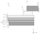
- FIG. 2 is a schematic cross-sectional view of the photoelectric conversion element taken along line 2A-2A in FIG.
- FIG. 3 is a schematic cross-sectional view of a photoelectric conversion element according to the second embodiment.
- FIG. 4 is a schematic cross-sectional view of a photoelectric conversion element according to the third embodiment.
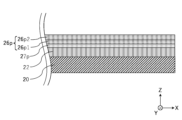
- FIG. 5 is a diagram for explaining one step in the method for manufacturing a photoelectric conversion element.
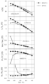
- FIG. 6 is a graph showing the temperature dependence of each characteristic of the photoelectric conversion element in the example and the reference example.
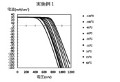
- FIG. 7 is a diagram showing the temperature dependence of the current-voltage characteristics of the photoelectric conversion element in Example 1.
- FIG. 1 is a schematic plan view of a photoelectric conversion element according to the first embodiment.
- FIG. 2 is a schematic cross-sectional view of the photoelectric conversion element taken along line 2A-2A in FIG.
- FIG. 3 is a schematic cross
- FIG. 8 is a diagram showing the temperature dependence of the current-voltage characteristics of the photoelectric conversion element in the reference example.
- FIG. 9 is a schematic plan view of a photovoltaic module including a photoelectric conversion element.
- FIG. 10 is a schematic perspective view of a flying object equipped with a photovoltaic module.
- Fig. 1 is a schematic plan view of a photoelectric conversion element according to one embodiment
- Fig. 2 is a schematic cross-sectional view of the photoelectric conversion element taken along line 2A-2A in Fig. 1.
- the photoelectric conversion element 10 may be a thin-film type photoelectric conversion element.
- the photoelectric conversion element 10 is a photovoltaic element that converts light energy into electrical energy.
- the photoelectric conversion element 10 has a substrate 20 that serves as a base on which each film is formed.
- the substrate 20 may be made of, for example, glass, ceramics, resin, or metal.
- the substrate 20 may be a flexible substrate. The shape and dimensions of the substrate 20 are determined appropriately depending on the size of the photoelectric conversion element 10, etc.
- the substrate 20 is formed of, for example, titanium (Ti), stainless steel (SUS), copper, aluminum, or an alloy of these.
- the substrate 20 may have a layered structure in which multiple metal base materials are layered, and for example, a stainless steel layer, a titanium layer, a molybdenum layer, or a molybdenum-sodium layer may be formed on the surface of the substrate.
- the photoelectric conversion element 10 may have a first electrode layer 22, a first buffer layer 27 on the first electrode layer 22, a photoelectric conversion layer 26 on the first buffer layer 27, a second buffer layer 28 on the photoelectric conversion layer 26, and a second electrode layer 24 on the second buffer layer 28.
- the photoelectric conversion layer 26 is provided between the first electrode layer 22 and the second electrode layer 24.
- the photoelectric conversion layer 26 is a layer that contributes to the mutual conversion between light energy and electrical energy.
- the photoelectric conversion layer 26 is sometimes called a light absorption layer.
- the first electrode layer 22 and the second electrode layer 24 are adjacent to the photoelectric conversion layer 26.
- adjacent means not only that both layers are in direct contact with each other, but also that both layers are close to each other via another layer.
- the second electrode layer 24 may be composed of a transparent electrode layer.
- the second electrode layer 24 is composed of a transparent electrode layer, light entering the photoelectric conversion layer 26 or exiting from the photoelectric conversion layer 26 passes through the second electrode layer 24.
- the first electrode layer 22 may be composed of an opaque electrode layer or a transparent electrode layer.
- the first electrode layer 22 is a layer that mainly contains molybdenum (Mo).
- Mo molybdenum
- the thickness of the first electrode layer 22 may be, for example, 50 nm to 1500 nm.
- the second electrode layer 24 may be formed of an n-type semiconductor, more specifically, a material having n-type conductivity and relatively low resistance.
- the second electrode layer 24 can function both as an n-type semiconductor and a transparent electrode layer.
- the second electrode layer 24 comprises, for example, a metal oxide to which a Group III element (B, Al, Ga, or In) is added as a dopant.
- a Group III element B, Al, Ga, or In
- the second electrode layer 24 can be selected from, for example, indium tin oxide (In 2 O 3 :Sn), indium titanium oxide (In 2 O 3 :Ti), indium zinc oxide (In 2 O 3 :Zn), tin zinc doped indium oxide (In 2 O 3 :Sn, Zn), tungsten doped indium oxide (In 2 O 3 :W), hydrogen doped indium oxide (In 2 O 3 :H), indium gallium zinc oxide (InGaZnO 4 ), zinc tin oxide (ZnO:Sn), fluorine doped tin oxide (SnO 2 :F), gallium doped zinc oxide (ZnO:Ga), boron doped zinc oxide (ZnO:B), aluminum doped zinc oxide (ZnO:Al), and the like.
- indium tin oxide In 2 O 3 :Sn
- indium titanium oxide In 2 O 3 :Ti
- indium zinc oxide In 2 O 3 :Zn
- the thickness of the second electrode layer 24 may be, for example, 500 nm to 2500 nm.
- the photoelectric conversion layer 26 may include, for example, a p-type semiconductor.
- the photoelectric conversion layer 26 may function as, for example, a polycrystalline or microcrystalline p-type compound semiconductor layer.
- the photoelectric conversion layer 26 is a layer containing a selenium compound.
- the selenium compound may be a group I-III-VI 2 compound semiconductor having a chalcopyrite structure.
- the group I element may be selected from copper (Cu), silver (Ag), gold (Au), etc.
- the group III element may be selected from indium (In), gallium (Ga), aluminum (Al), etc.
- the photoelectric conversion layer 26 contains selenium (Se) as a group VI element.
- the photoelectric conversion layer 26 may also contain sulfur (S), tellurium (Te), etc., in addition to selenium (Se) as a group VI element.
- the composition of the selenium compound constituting the photoelectric conversion layer 26 is preferably a compound represented by Cu(In,Ga)( Sx , Se1-x ) 2 .
- the selenium compound according to this composition only needs to contain at least one of indium and gallium.
- the symbol x in the composition is a real number satisfying "0 ⁇ x ⁇ 1" (the same applies below).
- the first buffer layer 27 is provided between the first electrode layer 22 and the photoelectric conversion layer 26.
- the first buffer layer has a compound layer containing A(S y , Se 1-y ) 2 as a main component, where y is a real number satisfying "0 ⁇ y ⁇ 1" (the same applies below).
- the element A is at least one of Nb and Ta. Therefore, the compound layer constituting the first buffer layer 27 may contain niobium selenide, niobium sulfoselenide, tantalum selenide, and/or tantalum sulfoselenide.
- the upper limit of the thickness of the region containing the largest proportion of the element A, excluding S and Se may be, for example, less than 100 nm, preferably less than 50 nm, more preferably less than 30 nm, even more preferably less than 15 nm, and most preferably 12 nm or less.
- the lower limit of the thickness of the region containing the largest proportion of the element A among elements other than S and Se may be, for example, 1 nm or more, preferably 3 nm or more, and more preferably 5 nm or more.
- the thickness of the region in the first buffer layer 27 that contains the largest proportion of element A among elements other than S and Se may be within a range that combines any of the above upper and lower limits.
- the upper and lower limits may be appropriately selected to optimize the characteristics of the photoelectric conversion element 10. From the viewpoint of suppressing peeling of the photoelectric conversion layer 26, it is preferable that the film thickness of the first buffer layer 27 is as small as possible.
- the compound layer containing A(S y , Se 1-y ) 2 in the first buffer layer 27 is formed by forming a layer containing element A on the Mo layer constituting the first electrode layer 22, forming a precursor film on the layer containing element A, and then selenizing or selenizing and sulfurizing.
- the thickness of the compound layer containing A(S y , Se 1-y ) 2 in the first buffer layer 27 may be increased by about 1.0 to 3.0 times due to selenization or selenization and sulfurization. Therefore, the thickness of the region in the first buffer layer 27 that contains the element A at the highest ratio among elements other than S and Se is considered to be about 1.0 to 3.0 times the thickness of the layer containing element A formed on the Mo layer during manufacturing.
- the first buffer layer 27 may be substantially made of a compound layer containing A(S y , Se 1-y ) 2.
- the first buffer layer 27 may include another layer different from the compound layer containing A(S y , Se 1-y ) 2 .
- the second buffer layer 28 may be a semiconductor material having the same conductivity type as the second electrode layer 24, or may be a semiconductor material having a different conductivity type.
- the second buffer layer 28 may be made of a material having a higher electrical resistance than the second electrode layer 24.
- the second buffer layer 28 is formed on the photoelectric conversion layer 26.
- the thickness of the second buffer layer 28 may be, for example, 10 nm to 100 nm.
- the second buffer layer 28 can be selected from compounds containing zinc (Zn), cadmium (Cd), and indium (In).
- compounds containing zinc include ZnO, ZnS, Zn(OH) 2 , or mixed crystals thereof such as Zn(O,S) and Zn(O,S,OH), as well as ZnMgO and ZnSnO.
- compounds containing cadmium include CdS, CdO, or mixed crystals thereof such as Cd(O,S) and Cd(O,S,OH).
- Examples of compounds containing indium include In 2 S 3 , In 2 O 3 , or mixed crystals thereof such as In 2 (O,S) 3 and In 2 (O,S,OH) 3 , and In 2 O 3 , In 2 S 3 , and In(OH) x can be used.
- the second buffer layer may also have a stacked structure of these compounds.
- the second buffer layer 28 has the effect of improving characteristics such as photoelectric conversion efficiency, but it is possible to omit it.
- the second buffer layer 28 is omitted, the second electrode layer 24 is formed directly on the photoelectric conversion layer 26.
- the photoelectric conversion element 10 may include a collecting electrode 30 on the second electrode layer 24.
- the collecting electrode 30 collects charge carriers from the second electrode layer 24 and is formed of a conductive material.
- the collecting electrode 30 may be in direct contact with the second electrode layer 24. From the viewpoint of improving power generation efficiency, it is preferable that the area of the collecting electrode 30 is as small as possible.
- the collecting electrode 30 may have a plurality of substantially linear first portions 31 and second portions 32 connected to the first portions 31.
- the first portions 31 may also be referred to as “fingers.”
- the second portions 32 may also be referred to as "bus bars.”
- the first portions 31 are arranged at intervals from one another.
- the multiple linear first portions 31 are connected to the second portions 32.
- the first portions 31 have the function of conducting electricity generated in the photoelectric conversion layer 26 to the second portions 32.
- the first portion 31 of the collecting electrode 30 may be arranged in a plurality of lines in the first direction (Y direction in the figure).
- the plurality of linear first portions 31 may be connected to the same second portion 32.
- the second portion 32 of the collecting electrode 30 may extend in a first direction (Y direction in the figure).
- the second portion 32 may be connected to the first portion 31 at an end of the first portion 31.
- the multiple first portions 31 may extend from the second portion 32 along the second direction (X direction in the figure).
- the second portion 32 of the collecting electrode 30 may extend in the first direction (the Y direction in the figure) substantially from near one end of the photoelectric conversion element 10 to near the other end.
- the width of the second portion 32 of the collecting electrode 30 (the width in the X direction in the figure) may be greater than the width of each of the first portions 31 (the width in the Y direction in the figure).
- the collecting electrode 30 (first portion 31 and second portion 32) may be made of a material having a higher conductivity than the material constituting the second electrode layer 24.
- the material constituting the collecting electrode 30 include indium tin oxide (In 2 O 3 :Sn), indium titanium oxide (In 2 O 3 :Ti), indium zinc oxide (In 2 O 3 :Zn), tin zinc doped indium oxide (In 2 O 3 :Sn, Zn), tungsten doped indium oxide (In 2 O 3 :W), hydrogen doped indium oxide (In 2 O 3 :H), indium gallium zinc oxide (InGaZnO 4 ), zinc tin oxide (ZnO:Sn), fluorine doped tin oxide (SnO 2 :F), aluminum-doped zinc oxide (ZnO:Al), boron-doped zinc oxide (ZnO:B), gallium-doped zinc oxide (ZnO:Ga), at least one of Ni, Ti, Cr, Mo, Al,
- the photoelectric conversion element 10 may include wiring 50 joined to the collecting electrode 30.
- the wiring 50 may be joined to the second portion 32 of the collecting electrode 30.
- the wiring 50 may be, for example, an interconnector for electrically connecting to the outside of the photoelectric conversion element 10, and/or a connector for connecting to a bypass diode that electrically bypasses a cell that cannot perform photoelectric conversion.
- the photoelectric conversion element 10 includes a collecting electrode 30 and wiring 50.
- the collecting electrode 30 and wiring 50 are not essential components, and the photoelectric conversion element 10 does not have to include the collecting electrode 30 and wiring 50.
- the photoelectric conversion element 10 may have an integrated structure in which multiple photoelectric conversion cells are integrated with each other. In this case, it is sufficient that one or each of the multiple photoelectric conversion cells has the first electrode layer 22 and first buffer layer 27 described above.
- the photoelectric conversion element 10 may also be a so-called tandem type photoelectric conversion element having a structure in which two photoelectric conversion cells are stacked on top of each other. In this case, it is sufficient that one or both of the two photoelectric conversion cells have the first electrode layer 22 and first buffer layer 27 described above.
- Fig. 3 is a schematic cross-sectional view of a photoelectric conversion element according to the second embodiment.
- the same components as those in the first embodiment are denoted by the same reference numerals. Please note that the description of the same components as those in the first embodiment may be omitted.
- the configuration of the photoelectric conversion module 10 in the second embodiment is the same as that in the first embodiment, except for the structure of the first buffer layer 27.
- the first buffer layer 27 has a compound layer 27a containing A(S y , Se 1-y ) 2 as a main component, and a layer 27b containing Mo(S z , Se 1-z ) 2 to which the element A has been added as a main component.
- the layer 27b containing Mo(S z , Se 1-z ) 2 to which the element A has been added is provided between the compound layer 27a and the first electrode layer 22.
- element A is at least one of Nb and Ta, as in the first embodiment.
- the upper limit of the thickness of the region (compound layer 27a) containing the largest proportion of element A among elements other than S and Se may be, for example, less than 100 nm, preferably less than 50 nm, more preferably less than 30 nm, even more preferably less than 15 nm, and most preferably 12 nm or less.
- the lower limit of the thickness of the region (compound layer 27a) containing the largest proportion of element A among elements other than S and Se may be, for example, 1 nm or more, preferably 3 nm or more, and more preferably 5 nm or more.
- the thickness of the region in the first buffer layer 27 that contains the largest proportion of element A among elements other than S and Se may be within a range that combines any of the above upper and lower limits.
- the upper and lower limits may be appropriately selected to optimize the characteristics of the photoelectric conversion element 10.
- Fig. 4 is a schematic cross-sectional view of a photoelectric conversion element according to the second embodiment.
- the same components as those in the first embodiment are denoted by the same reference numerals. Please note that the description of the same components as those in the first embodiment may be omitted.
- the configuration of the photoelectric conversion module 10 in the third embodiment is the same as that in the first embodiment, except for the structure of the first buffer layer 27.
- the first buffer layer 27 has a compound layer 27a containing A(S y , Se 1-y ) 2 as a main component, and a layer 27c containing element A as a main component.
- the layer 27c containing element A is provided between the compound layer 27a and the first electrode layer 22.
- y is a real number that satisfies "0 ⁇ y ⁇ 1" (the same applies below).
- element A is at least one of Nb and Ta, as in the first embodiment.
- the upper limit of the thickness of the region (compound layer 27a) containing the largest proportion of element A among elements other than S and Se may be, for example, less than 100 nm, preferably less than 50 nm, more preferably less than 30 nm, even more preferably less than 15 nm, and most preferably 12 nm or less.
- the lower limit of the thickness of the region (compound layer 27a) containing the largest proportion of element A among elements other than S and Se may be, for example, 1 nm or more, preferably 3 nm or more, and more preferably 5 nm or more.
- the thickness of the region in the first buffer layer 27 that contains the largest proportion of element A among elements other than S and Se may be within a range that combines any of the above upper and lower limits.
- the upper and lower limits may be appropriately selected to optimize the characteristics of the photoelectric conversion element 10.
- Fig. 5 is a diagram for explaining one step in the method for manufacturing a photoelectric conversion element.
- Fig. 5 shows a state in which a precursor film, which will be described later, has been formed.
- a layer containing Mo is formed on the substrate 20.
- the layer containing Mo is formed on the surface of the substrate 20 by, for example, a sputtering method.
- the sputtering method may be a direct current (DC) sputtering method or a radio frequency (RF) sputtering method.
- the layer containing Mo may be formed by a chemical vapor deposition (CVD) method, an atomic layer deposition (ALD) method, or the like, instead of the sputtering method.
- the layer containing Mo is formed as a material constituting the first electrode layer 22.
- a layer 27p containing at least one of element A, Nb and Ta, is formed on the layer containing Mo.
- the layer 27p containing element A is formed by a sputtering method, for example, physical vapor deposition (PVD).
- the sputtering method may be a direct current (DC) sputtering method or a radio frequency (RF) sputtering method.
- the physical vapor deposition (PVD) may be, for example, an electron beam deposition method or a pulsed laser method.
- the layer 27p containing element A may be formed by using a chemical vapor deposition (CVD) method, an atomic layer deposition (ALD) method, or the like.
- CVD chemical vapor deposition
- ALD atomic layer deposition
- the layer 27p containing element A is formed to a thickness of, for example, less than 50 nm, preferably less than 30 nm, more preferably less than 15 nm, and even more preferably 12 nm or less.
- the layer 27p containing element A is formed to a thickness of, for example, 1 nm or more, preferably 3 nm or more, and more preferably 5 nm or more.
- the thickness of the layer 27p containing element A may be within a range that arbitrarily combines the above upper limit value and the above lower limit value.
- the thickness of the layer 27p containing element A may be appropriately selected so as to optimize the characteristics of the photoelectric conversion element 10 after manufacture. From the viewpoint of suppressing peeling of the photoelectric conversion layer 26 after the chalcogenization step described below, it is preferable that the thickness of the layer 27p containing element A is as small as possible.
- the precursor film 26p is a precursor for forming the photoelectric conversion layer 26.
- the precursor film 26p may be a laminate including a film 26p1 containing a group III element and a film 26p2 containing a group I element. Specifically, after the film 26p1 containing a group III element is formed on the layer 27p containing element A, the film 26p2 containing a group I element may be formed on the film 26p1 containing a group III element.
- the material constituting the film 26p2 containing a group I element can be selected from, for example, Ag, Cu, Au, etc.
- the material constituting the film 26p1 containing a group III element can be selected from, for example, indium, gallium, aluminum, etc.
- the precursor film 26p may additionally contain an alkali metal such as Li, Na, K, Rb, Cs, etc.
- the precursor film 26p can be formed, for example, by physical vapor deposition (PVD).
- PVD physical vapor deposition
- Examples of physical vapor deposition (PVD) include sputtering and evaporation. Evaporation is a method of forming a film using atoms that have become gaseous by heating an evaporation source. Note that FIG. 5 shows the state after the formation of the precursor film 26p has been completed and before the selenization step described below is started.
- the precursor film 26p is selenized or the precursor film 26p is selenized and sulfurized to form a photoelectric conversion layer 26 containing a selenium compound (chalcogenization step).
- selenization is first performed by a gas-phase selenization method.
- Selenization is performed by heating the precursor film 26p in an atmosphere of a selenium source gas (e.g., hydrogen selenide or selenium vapor) containing selenium as a group VI element source.
- a selenium source gas e.g., hydrogen selenide or selenium vapor
- selenization is preferably performed at a temperature in the range of 300°C to 600°C in a heating furnace, for example.
- the precursor film 26p is converted into a selenium compound containing a group I element, a group III element, and selenium.
- selenization may be performed by a method other than the gas-phase selenization method.
- Selenization can also be performed by, for example, a solid-phase selenization method, a vapor deposition method, an ink application method, and/or an electrodeposition method.
- the selenium compound containing group I and group III elements and selenium is sulfurized.
- the sulfurization is performed by heating the selenium compound in an atmosphere of a sulfur-containing sulfur source gas (e.g., hydrogen sulfide or sulfur vapor).
- a sulfur-containing sulfur source gas e.g., hydrogen sulfide or sulfur vapor.
- the sulfur source gas serves to replace selenium with sulfur in crystals consisting of group I and group III elements and selenium, for example, chalcopyrite crystals.
- sulfurization be carried out at a temperature in the range of 450°C to 650°C in a heating furnace, for example.
- the precursor film 26p is selenized and sulfurized.
- the precursor film 26p may be only selenized without being sulfurized.
- the precursor film 26p is converted into the above-mentioned photoelectric conversion layer 26.
- a compound layer containing A(S y , Se 1-y ) 2 is formed together with the formation of the selenium compound constituting the photoelectric conversion layer 26.
- y is a real number that satisfies "0 ⁇ y ⁇ 1".
- the compound layer containing A(S y , Se 1-y ) 2 is formed by selenizing or selenizing and sulfurizing at least a part of the layer 27p containing the element A. Therefore, the element A contains at least one of Nb and Ta.
- the compound layer containing A(S y , Se 1-y ) 2 is a component of the first buffer layer 27 described in the first, second and third embodiments.
- selenization and sulfurization are performed, y may be in a range that satisfies "0 ⁇ y ⁇ 1".
- the first buffer layer 27 is composed of a compound layer containing A(S y , Se 1-y ) 2. This provides the first buffer layer 27 described in the first embodiment.
- the first buffer layer 27 has a compound layer 27a containing A(S y , Se 1-y ) 2 and a layer 27b containing Mo(S z , Se 1-z ) 2 to which the element A is added.
- z is a real number satisfying "0 ⁇ z ⁇ 1".
- the layer 27b containing Mo(S z , Se 1-z ) 2 to which the element A is added is formed by selenizing or selenizing and sulfurizing a part of the surface side of the layer containing Mo, and doping the upper layer with the element A. Therefore, the layer 27b containing Mo(S z ,Se 1-z ) 2 to which the element A is added is located between the compound layer 27a containing A(S y ,Se 1-y ) 2 and the first electrode layer 22. In this manner, the first buffer layer 27 described in the second embodiment is obtained.
- the first buffer layer 27 has a compound layer 27a containing A(S y , Se 1-y ) 2 and a layer 27c containing element A.
- the layer 27c containing element A is located between the compound layer 27a containing A(S y , Se 1-y ) 2 and the first electrode layer 22. In this manner, the first buffer layer 27 described in the third embodiment is obtained.
- a second buffer layer 28 is formed on the photoelectric conversion layer 26 formed in the chalcogenization step, if necessary.
- the second buffer layer 28 can be formed by a method such as CBD (chemical bath deposition), sputtering, CVD, or ALD.
- the materials constituting the second buffer layer are as described above. If the second buffer layer 28 is not required, it does not need to be formed.
- the second electrode layer 24 is formed on the photoelectric conversion layer 26 or the second buffer layer 28.
- the second electrode layer 24 is formed by a method such as sputtering, CVD, or ALD.
- the material constituting the second electrode layer 24 is as described above.
- the collecting electrode 30 (first portion 31 and second portion 32) may be formed, and the wiring 50 may be formed.
- the photoelectric conversion element described in the first, second, and third embodiments is obtained.
- the precursor film 26p is formed directly on the layer containing Mo.
- the first buffer layer 27 is substantially formed of Mo(S y , Se 1 -y ) 2. That is, the photoelectric conversion layer 26 is in contact with Mo(S y , Se 1-y ) 2 as the first buffer layer 27.
- A(S y , Se 1-y ) 2 is expected to be a metallic layer.
- the A(S y , Se 1-y ) 2 layer is considered to be a metal-semiconductor junction including an ohmic junction due to the junction with the photoelectric conversion layer (p-type semiconductor) containing a selenium compound. Therefore, it is presumed that the carrier mobility characteristics can be maintained in a low-temperature environment.
- the first buffer layer is composed of two layers of Mo(S y ,Se 1-y ) 2
- Mo(S y ,Se 1-y ) 2 is known as a semiconductor, and a band structure having a Schottky barrier is formed by junction with a photoelectric conversion layer (p-type semiconductor) containing a selenium compound. Therefore, it is presumed that the carrier mobility is reduced by the Schottky barrier at low temperatures.
- the photoelectric conversion element 10 according to the first, second and third embodiments can maintain its photoelectric conversion performance even in a low temperature environment, compared to the above reference example.
- Example 1 Next, the photoelectric conversion element according to Example 1 will be described.
- the first electrode layer 22, the first buffer layer 27, the photoelectric conversion layer 26, the second buffer layer 28, and the second electrode layer 24 are laminated in this order on the MoNa layer on the titanium substrate.
- the first electrode layer 22 is made of molybdenum.
- the first buffer layer 27 includes a compound layer made of Nb(S y , Se 1-y ) 2.
- the first buffer layer 27 is assumed to have a compound layer 27a containing Nb(S y , Se 1-y ) 2 as a main component, and a layer 27b containing Mo(S z , Se 1-z ) 2 to which Nb is added as a main component (the aspect described in the second embodiment).
- the photoelectric conversion layer 26 is a Cu(In, Ga)(S x , Se 1-x ) 2 layer.
- the second buffer layer 28 is made of CdS.
- the second electrode layer 24 is made of In2O3 .
- a Mo layer was formed as the first electrode layer 22 on the MoNa layer on the titanium substrate, an Nb layer was formed on the Mo layer, and a predetermined precursor film (Cu(In,Ga) film) was formed on the Nb layer.
- the thickness of the formed Nb layer was 9 nm.
- first buffer layer 27 and a photoelectric conversion layer 26 were selenized and sulfurized as described above to form a first buffer layer 27 and a photoelectric conversion layer 26.
- second buffer layer 28 and a second electrode layer 24 were formed in this order on the photoelectric conversion layer 26.
- ⁇ _STD , Voc _STD , FF _STD and Rs _STD respectively mean the photoelectric conversion efficiency, open circuit voltage, fill factor and series resistance of the photoelectric conversion element at a temperature of 25° C. Therefore, the photoelectric conversion efficiency ratio ( ⁇ / ⁇ _STD ), open circuit voltage ratio (Voc/Voc _STD ), fill factor ratio (FF/FF _STD ) and series resistance ratio (Rs/Rs _STD ) correspond to values obtained by dividing the photoelectric conversion efficiency, open circuit voltage, fill factor and series resistance at each temperature by the photoelectric conversion efficiency, open circuit voltage, fill factor and series resistance at 25° C.
- the photoelectric conversion efficiency ( ⁇ ) in Example 1 increases with decreasing temperature.
- the photoelectric conversion efficiency in the Reference Example increases with decreasing temperature in the range of 25°C to -80°C.
- the rate of increase in photoelectric conversion efficiency with decreasing temperature is low in the range of -30°C to -80°C (see also the photoelectric conversion efficiency ratio graph).
- the photoelectric conversion efficiency does not increase at temperatures below -80°C.
- the photoelectric conversion efficiency in Example 1 is higher than that in the Reference Example at temperatures below -90°C.
- the fill factor ratio (FF/ FF_STD ) in Example 1 increases with decreasing temperature.
- the fill factor ratio in the Reference Example decreases with decreasing temperature below approximately ⁇ 30° C. to ⁇ 60° C. It is considered that the fill factor in the Reference Example is lower at temperatures of ⁇ 90° C. or lower than the fill factor at 25° C.
- the series resistance ratio (Rs/ Rs_STD ) in Example 1 decreases slightly with decreasing temperature.
- the series resistance ratio in the Reference Example increases sharply with decreasing temperature at temperatures of -30°C to -40°C or lower.
- the series resistance ratio in Example 1 is significantly smaller than that in the Reference Example at temperatures of -30°C to -40°C or lower. Therefore, it is considered that the photoelectric conversion element according to Example 1 may be more significant in terms of photoelectric conversion than the photoelectric conversion element according to the Reference Example at temperatures lower than -30°C to -40°C.
- FIG. 7 is a diagram showing the temperature dependence of the current-voltage characteristics of the photoelectric conversion element in Example 1.
- FIG. 8 is a diagram showing the temperature dependence of the current-voltage characteristics of the photoelectric conversion element in Reference Example.
- the multiple lines in the graph indicate, from the left, the current-voltage characteristics at 60° C., 25° C., 10° C., ⁇ 10° C., ⁇ 30° C., ⁇ 60° C., ⁇ 80° C., ⁇ 100° C., and ⁇ 120° C.
- the multiple lines in the graph indicate, from the left, the current-voltage characteristics at 120° C., 80° C., 60° C., 25° C., 10° C., 0° C., ⁇ 10° C., ⁇ 30° C., ⁇ 60° C., ⁇ 80° C., ⁇ 100° C., and ⁇ 120° C.
- the photoelectric conversion element of Example 1 at any temperature in the range of 60°C to -120°C, as the voltage increases, the current decreases in an upwardly convex curve. In this way, the photoelectric conversion element of Example 1 exhibits normal current-voltage characteristics at temperatures in the range of 60°C to -120°C.
- the measurement results of the current-voltage characteristics show that the photoelectric conversion element of Example 1 has the potential to maintain its photoelectric conversion performance even in a low-temperature environment.
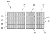
- FIG. 9 is a schematic plan view of a photovoltaic module including a photoelectric conversion element.
- a photovoltaic module 300 may include one or a plurality of photoelectric conversion elements 10.
- Fig. 9 shows a photovoltaic module 300 including a plurality of photoelectric conversion elements 10.
- the one or a plurality of photoelectric conversion elements 10 may be sealed by, for example, a sealing material.
- the multiple photoelectric conversion elements 10 may be arranged in at least one direction, and preferably in a lattice pattern. In this case, the multiple photoelectric conversion elements 10 may be electrically connected to each other in series and/or parallel.
- the photoelectric conversion elements 10 are arranged so as to partially overlap each other.
- adjacent photoelectric conversion elements 10 partially overlap each other.
- a certain photoelectric conversion element 10 may be arranged so as to cover the second portion 32 of the collecting electrode 30 of the photoelectric conversion element 10 adjacent to it.
- adjacent photoelectric conversion elements 10 may be arranged with a gap between them.
- the wiring 50 described above may electrically connect adjacent photoelectric conversion elements 10 to each other.
- FIG. 10 is a schematic perspective view of a flying object equipped with a photovoltaic power generation module.
- the flying object 900 may have a base 910 and a wing 920.
- the wing portion 920 may include the photovoltaic module 300 described above.
- the wing portion 920 includes a plurality of photovoltaic modules 300. Since the flying object 900 is exposed to a low-temperature environment during operation, it is desirable to use a photovoltaic module 300 including the photoelectric conversion element 10 described above. There is no particular limit to the flying altitude of the flying object 900 during operation.
- the flying object 900 may fly in the stratosphere, for example. In this case, the flying object 900 may be exposed to a temperature environment of -70°C to -100°C.
- the flying object 900 has wing portions 920.
- the flying object 900 does not have to have wing portions 920.
- the flying object 900 may have a shape similar to an airship or a balloon, for example.
- the flying object 900 may include one or more photovoltaic modules 300.
- the photovoltaic modules 300 may generate electricity from sunlight, or may generate electricity from light other than sunlight.
Landscapes
- Engineering & Computer Science (AREA)
- Aviation & Aerospace Engineering (AREA)
- Mechanical Engineering (AREA)
- Remote Sensing (AREA)
- Chemical & Material Sciences (AREA)
- Combustion & Propulsion (AREA)
- Photovoltaic Devices (AREA)
Priority Applications (2)
| Application Number | Priority Date | Filing Date | Title |
|---|---|---|---|
| EP24779904.2A EP4693418A1 (en) | 2023-03-31 | 2024-03-21 | Photoelectric conversion element, photovoltaic module, flying object and method for manufacturing photoelectric conversion element |
| JP2025510682A JPWO2024203785A1 (https=) | 2023-03-31 | 2024-03-21 |
Applications Claiming Priority (2)
| Application Number | Priority Date | Filing Date | Title |
|---|---|---|---|
| JP2023059625 | 2023-03-31 | ||
| JP2023-059625 | 2023-03-31 |
Publications (1)
| Publication Number | Publication Date |
|---|---|
| WO2024203785A1 true WO2024203785A1 (ja) | 2024-10-03 |
Family
ID=92906320
Family Applications (1)
| Application Number | Title | Priority Date | Filing Date |
|---|---|---|---|
| PCT/JP2024/011172 Ceased WO2024203785A1 (ja) | 2023-03-31 | 2024-03-21 | 光電変換素子、光発電モジュール、飛翔体及び光電変換素子の製造方法 |
Country Status (3)
| Country | Link |
|---|---|
| EP (1) | EP4693418A1 (https=) |
| JP (1) | JPWO2024203785A1 (https=) |
| WO (1) | WO2024203785A1 (https=) |
Citations (7)
| Publication number | Priority date | Publication date | Assignee | Title |
|---|---|---|---|---|
| JPH10512096A (ja) * | 1994-10-21 | 1998-11-17 | ノルディック ソーラー エナジイ アクチボラゲット | 薄膜太陽電池の製法 |
| JP2014049572A (ja) | 2012-08-30 | 2014-03-17 | Toyota Central R&D Labs Inc | 光電素子用電極 |
| JP2015509288A (ja) * | 2012-01-19 | 2015-03-26 | ヌボサン,インコーポレイテッド | 光電池用保護コーティング |
| JP2015513230A (ja) * | 2012-04-12 | 2015-04-30 | ローベルト ボツシユ ゲゼルシヤフト ミツト ベシユレンクテル ハフツングRobert Bosch Gmbh | 光起電力による薄膜ソーラモジュールならびに該薄膜ソーラモジュールの製造方法 |
| JP2015514325A (ja) * | 2012-04-02 | 2015-05-18 | ローベルト ボツシユ ゲゼルシヤフト ミツト ベシユレンクテル ハフツングRobert Bosch Gmbh | 光起電性薄膜太陽電池セル用の多層裏面電極、該多層裏面電極を薄膜太陽電池セル及びモジュールの製造に使用する方法、多層裏面電極を含んだ光起電性薄膜太陽電池セル及びモジュール並びにその製造方法 |
| CN208622756U (zh) * | 2018-08-03 | 2019-03-19 | 黑龙江华夏易能新能源科技有限公司 | 一种太阳能电池 |
| JP2023059625A (ja) | 2021-10-15 | 2023-04-27 | 日本軽金属株式会社 | 金属部材の製造方法及び金属樹脂接合体の製造方法 |
-
2024
- 2024-03-21 EP EP24779904.2A patent/EP4693418A1/en active Pending
- 2024-03-21 JP JP2025510682A patent/JPWO2024203785A1/ja active Pending
- 2024-03-21 WO PCT/JP2024/011172 patent/WO2024203785A1/ja not_active Ceased
Patent Citations (7)
| Publication number | Priority date | Publication date | Assignee | Title |
|---|---|---|---|---|
| JPH10512096A (ja) * | 1994-10-21 | 1998-11-17 | ノルディック ソーラー エナジイ アクチボラゲット | 薄膜太陽電池の製法 |
| JP2015509288A (ja) * | 2012-01-19 | 2015-03-26 | ヌボサン,インコーポレイテッド | 光電池用保護コーティング |
| JP2015514325A (ja) * | 2012-04-02 | 2015-05-18 | ローベルト ボツシユ ゲゼルシヤフト ミツト ベシユレンクテル ハフツングRobert Bosch Gmbh | 光起電性薄膜太陽電池セル用の多層裏面電極、該多層裏面電極を薄膜太陽電池セル及びモジュールの製造に使用する方法、多層裏面電極を含んだ光起電性薄膜太陽電池セル及びモジュール並びにその製造方法 |
| JP2015513230A (ja) * | 2012-04-12 | 2015-04-30 | ローベルト ボツシユ ゲゼルシヤフト ミツト ベシユレンクテル ハフツングRobert Bosch Gmbh | 光起電力による薄膜ソーラモジュールならびに該薄膜ソーラモジュールの製造方法 |
| JP2014049572A (ja) | 2012-08-30 | 2014-03-17 | Toyota Central R&D Labs Inc | 光電素子用電極 |
| CN208622756U (zh) * | 2018-08-03 | 2019-03-19 | 黑龙江华夏易能新能源科技有限公司 | 一种太阳能电池 |
| JP2023059625A (ja) | 2021-10-15 | 2023-04-27 | 日本軽金属株式会社 | 金属部材の製造方法及び金属樹脂接合体の製造方法 |
Non-Patent Citations (1)
| Title |
|---|
| See also references of EP4693418A1 |
Also Published As
| Publication number | Publication date |
|---|---|
| EP4693418A1 (en) | 2026-02-11 |
| JPWO2024203785A1 (https=) | 2024-10-03 |
Similar Documents
| Publication | Publication Date | Title |
|---|---|---|
| US8575478B2 (en) | Integrated structure of CIS based solar cell | |
| CN102315323B (zh) | 光伏电池以及用于形成光伏电池的背接触的方法 | |
| TWI478367B (zh) | 太陽能電池及其製造方法 | |
| EP2202804A2 (en) | Method of fabricating a CIGSS solar cell | |
| US8871560B2 (en) | Plasma annealing of thin film solar cells | |
| EP2487724A2 (en) | Photovoltaic power-generating apparatus and method for manufacturing same | |
| KR20140099865A (ko) | 광전지용 전도성 기판 | |
| EP2426731A2 (en) | Solar power generation apparatus and manufacturing method thereof | |
| JP2016063160A (ja) | 光電変換素子および太陽電池 | |
| US20140053904A1 (en) | Photoelectric conversion element and solar cell | |
| KR101428146B1 (ko) | 태양전지 모듈 및 이의 제조방법 | |
| US9306098B2 (en) | Method of making photovoltaic device comprising an absorber having a surface layer | |
| JP2019057701A (ja) | 太陽電池、多接合型太陽電池、太陽電池モジュール、太陽光発電システム及び太陽電池の製造方法 | |
| JP2007335625A (ja) | 太陽電池 | |
| US20170077327A1 (en) | Photoelectric conversion element, solar cell, solar cell module, and solar power generating system | |
| US20140053903A1 (en) | Photoelectric conversion element and solar cell | |
| WO2024203785A1 (ja) | 光電変換素子、光発電モジュール、飛翔体及び光電変換素子の製造方法 | |
| JP7569218B2 (ja) | 光電変換素子および光電変換素子の製造方法 | |
| KR101326970B1 (ko) | 태양전지 모듈 및 이의 제조방법 | |
| JP2019009241A (ja) | 太陽電池およびその製造方法 | |
| US20150249171A1 (en) | Method of making photovoltaic device comprising i-iii-vi2 compound absorber having tailored atomic distribution | |
| JP7058460B2 (ja) | 光電変換モジュール | |
| US9653628B2 (en) | Absorber layer for photovoltaic device, and method of making the same | |
| EP4365959A1 (en) | Photoelectric conversion element and method for manufacturing photoelectric conversion element | |
| JP7194581B2 (ja) | 光電変換素子 |
Legal Events
| Date | Code | Title | Description |
|---|---|---|---|
| 121 | Ep: the epo has been informed by wipo that ep was designated in this application |
Ref document number: 24779904 Country of ref document: EP Kind code of ref document: A1 |
|
| ENP | Entry into the national phase |
Ref document number: 2025510682 Country of ref document: JP Kind code of ref document: A |
|
| WWE | Wipo information: entry into national phase |
Ref document number: 2025510682 Country of ref document: JP |
|
| WWE | Wipo information: entry into national phase |
Ref document number: 2024779904 Country of ref document: EP |
|
| NENP | Non-entry into the national phase |
Ref country code: DE |
|
| ENP | Entry into the national phase |
Ref document number: 2024779904 Country of ref document: EP Effective date: 20251031 |
|
| ENP | Entry into the national phase |
Ref document number: 2024779904 Country of ref document: EP Effective date: 20251031 |
|
| ENP | Entry into the national phase |
Ref document number: 2024779904 Country of ref document: EP Effective date: 20251031 |
|
| ENP | Entry into the national phase |
Ref document number: 2024779904 Country of ref document: EP Effective date: 20251031 |
|
| ENP | Entry into the national phase |
Ref document number: 2024779904 Country of ref document: EP Effective date: 20251031 |
|
| ENP | Entry into the national phase |
Ref document number: 2024779904 Country of ref document: EP Effective date: 20251031 |
|
| ENP | Entry into the national phase |
Ref document number: 2024779904 Country of ref document: EP Effective date: 20251031 |
|
| ENP | Entry into the national phase |
Ref document number: 2024779904 Country of ref document: EP Effective date: 20251031 |
|
| WWP | Wipo information: published in national office |
Ref document number: 2024779904 Country of ref document: EP |