WO2024203736A1 - 半導体素子搭載用基板 - Google Patents
半導体素子搭載用基板 Download PDFInfo
- Publication number
- WO2024203736A1 WO2024203736A1 PCT/JP2024/011069 JP2024011069W WO2024203736A1 WO 2024203736 A1 WO2024203736 A1 WO 2024203736A1 JP 2024011069 W JP2024011069 W JP 2024011069W WO 2024203736 A1 WO2024203736 A1 WO 2024203736A1
- Authority
- WO
- WIPO (PCT)
- Prior art keywords
- semiconductor element
- substrate
- protective layer
- element mounting
- layer
- Prior art date
- Legal status (The legal status is an assumption and is not a legal conclusion. Google has not performed a legal analysis and makes no representation as to the accuracy of the status listed.)
- Ceased
Links
Images


Classifications
-
- H—ELECTRICITY
- H10—SEMICONDUCTOR DEVICES; ELECTRIC SOLID-STATE DEVICES NOT OTHERWISE PROVIDED FOR
- H10W—GENERIC PACKAGES, INTERCONNECTIONS, CONNECTORS OR OTHER CONSTRUCTIONAL DETAILS OF DEVICES COVERED BY CLASS H10
- H10W40/00—Arrangements for thermal protection or thermal control
- H10W40/20—Arrangements for cooling
-
- H—ELECTRICITY
- H05—ELECTRIC TECHNIQUES NOT OTHERWISE PROVIDED FOR
- H05K—PRINTED CIRCUITS; CASINGS OR CONSTRUCTIONAL DETAILS OF ELECTRIC APPARATUS; MANUFACTURE OF ASSEMBLAGES OF ELECTRICAL COMPONENTS
- H05K1/00—Printed circuits
- H05K1/02—Details
-
- H—ELECTRICITY
- H10—SEMICONDUCTOR DEVICES; ELECTRIC SOLID-STATE DEVICES NOT OTHERWISE PROVIDED FOR
- H10H—INORGANIC LIGHT-EMITTING SEMICONDUCTOR DEVICES HAVING POTENTIAL BARRIERS
- H10H20/00—Individual inorganic light-emitting semiconductor devices having potential barriers, e.g. light-emitting diodes [LED]
- H10H20/01—Manufacture or treatment
- H10H20/036—Manufacture or treatment of packages
- H10H20/0365—Manufacture or treatment of packages of means for heat extraction or cooling
-
- H—ELECTRICITY
- H10—SEMICONDUCTOR DEVICES; ELECTRIC SOLID-STATE DEVICES NOT OTHERWISE PROVIDED FOR
- H10H—INORGANIC LIGHT-EMITTING SEMICONDUCTOR DEVICES HAVING POTENTIAL BARRIERS
- H10H20/00—Individual inorganic light-emitting semiconductor devices having potential barriers, e.g. light-emitting diodes [LED]
- H10H20/80—Constructional details
- H10H20/85—Packages
- H10H20/857—Interconnections, e.g. lead-frames, bond wires or solder balls
-
- H—ELECTRICITY
- H10—SEMICONDUCTOR DEVICES; ELECTRIC SOLID-STATE DEVICES NOT OTHERWISE PROVIDED FOR
- H10H—INORGANIC LIGHT-EMITTING SEMICONDUCTOR DEVICES HAVING POTENTIAL BARRIERS
- H10H20/00—Individual inorganic light-emitting semiconductor devices having potential barriers, e.g. light-emitting diodes [LED]
- H10H20/80—Constructional details
- H10H20/85—Packages
- H10H20/858—Means for heat extraction or cooling
- H10H20/8581—Means for heat extraction or cooling characterised by their material
-
- H—ELECTRICITY
- H10—SEMICONDUCTOR DEVICES; ELECTRIC SOLID-STATE DEVICES NOT OTHERWISE PROVIDED FOR
- H10W—GENERIC PACKAGES, INTERCONNECTIONS, CONNECTORS OR OTHER CONSTRUCTIONAL DETAILS OF DEVICES COVERED BY CLASS H10
- H10W70/00—Package substrates; Interposers; Redistribution layers [RDL]
- H10W70/60—Insulating or insulated package substrates; Interposers; Redistribution layers
- H10W70/67—Insulating or insulated package substrates; Interposers; Redistribution layers characterised by their insulating layers or insulating parts
- H10W70/69—Insulating materials thereof
Definitions
- the present invention relates to a substrate for mounting semiconductor elements.
- Patent Document 1 discloses a substrate for mounting semiconductor elements that includes a base material made of metal, an insulating layer, and an intermediate layer disposed between the base material and the insulating layer.
- Patent Document 1 Even with prior art such as Patent Document 1, there was still room for improvement in the technology for suppressing corrosion of the substrate in a substrate for mounting semiconductor elements.
- the substrate for mounting semiconductor elements described in Patent Document 1 the substrate is formed from metal, so when a semiconductor element is mounted on the substrate for mounting semiconductor elements and used, there was a risk of the substrate corroding if salt water adheres to the substrate. For this reason, a technology for suppressing corrosion of the substrate was desired.
- the present invention aims to provide a technology that suppresses corrosion of the base material in substrates for mounting semiconductor elements.
- the present invention has been made to solve at least some of the problems described above, and can be realized in the following form.
- a substrate for mounting semiconductor elements includes a base material made of metal, an electrode connected to a semiconductor element, and a protective layer disposed between the base material and the electrode, the protective layer being made of a material that is more corrosion resistant than the metal forming the base material.
- the protective layer disposed between the metal substrate and the electrode is made of a material that is more corrosion-resistant than the metal that forms the substrate. This makes it possible to suppress corrosion of the substrate.
- the base material may be formed in a flat plate shape, and the protective layer may cover a pair of main surfaces of the base material and a side surface formed between the pair of main surfaces.
- the base material formed in a flat plate shape has a pair of main surfaces and a side surface formed between the pair of main surfaces covered by the protective layer. This prevents the surface of the base material from being exposed, further suppressing corrosion of the base material.
- the thickness of the protective layer may be smaller than the thickness of the base material.
- the protective layer may be formed of a metal containing as a main component any one of nickel, gold, palladium, titanium, molybdenum, tungsten, platinum, silver, lead, and tin.
- the metal that forms the protective layer and contains as a main component any one of nickel, gold, palladium, titanium, molybdenum, tungsten, platinum, silver, lead, and tin can be easily formed by plating. This allows the protective layer to be formed relatively easily in the manufacturing process of the semiconductor element mounting substrate.
- the semiconductor element mounting substrate of the above embodiment may further include an insulating layer disposed between the substrate and the electrode, and an adhesion layer disposed between the insulating layer and the protective layer and in close contact with the insulating layer and the protective layer.
- the adhesion layer can be provided to bring the insulating layer and the protective layer into close contact with each other, so that the protective layer can suppress corrosion of the substrate while suppressing peeling of the insulating layer from the substrate.
- the adhesion layer may be formed of a metal containing one of titanium, chromium, and molybdenum as a main component. According to this configuration, by using an adhesion layer formed of a metal containing one of titanium, chromium, and molybdenum as a main component, it is possible to further prevent the insulating layer from peeling off from the substrate while suppressing corrosion of the substrate by the protective layer.
- the present invention can be realized in various forms, for example, in the form of a product including a substrate for mounting semiconductor elements, a method for manufacturing a substrate for mounting semiconductor elements, etc.
- FIG. 1 is a schematic cross-sectional view of a semiconductor element mounting board according to a first embodiment.
- 1 is a schematic cross-sectional view of a semiconductor package according to a first embodiment;
- FIG. 5 is a schematic cross-sectional view of a semiconductor element mounting board according to a second embodiment.
- 4 is a cross-sectional view taken along line AA in FIG. 3.
- 5 is a schematic cross-sectional view of a modified example of the semiconductor element mounting board of the first embodiment.
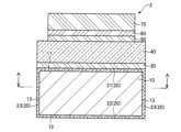
- FIG. 1 is a schematic cross-sectional view of a semiconductor device mounting board 1 according to the first embodiment.
- FIG. 2 is a schematic cross-sectional view of a semiconductor package 5 according to the first embodiment.
- the semiconductor device mounting board 1 according to the present embodiment supports an optical semiconductor such as a light emitting diode (LED) or a semiconductor laser (LD) as a semiconductor device 5a, and functions as a heat dissipation board that dissipates heat generated during light emission to the outside.
- the semiconductor device mounting board 1 includes a base material 10, a protective layer 20, an adhesion layer 30, an insulating layer 40, an adhesion layer 50, a bonding layer 60, and an electrode 70.
- the thickness relationships of the base material 10, the protective layer 20, the adhesion layer 30, the insulating layer 40, the adhesion layer 50, the bonding layer 60, the electrode 70, and the semiconductor device 5a in FIG. 1 and FIG. 2 are illustrated so as to be different from the actual thickness relationships for the sake of convenience of explanation.
- the substrate 10 is a member having a flat plate shape, and serves as the base of the semiconductor element mounting substrate 1. In this embodiment, the thickness of the substrate 10 is 1 mm.
- the substrate 10 is made of a metal. In this embodiment, the substrate 10 is made of copper (Cu).
- the substrate 10 may be made of a material whose main component is copper, aluminum (Al), or a material whose main component is aluminum.
- the term "main component” refers to a component that is greater than 50% by mass in the target material.
- the substrate 10 may be made of an alloy of copper and aluminum.
- the protective layer 20 is formed on each of the pair of main surfaces 11, 12 of the substrate 10.
- the protective layer 20 has a protective layer 21 formed on one of the pair of main surfaces 11, 12, and a protective layer 22 formed on the other main surface 12.
- the protective layer 21 is disposed between the substrate 10 and the electrode 70, more specifically, between the substrate 10 and the adhesion layer 30.
- the protective layer 20 is formed of a material that is more resistant to corrosion by salt water than the copper that forms the base material 10.
- corrosion resistance to salt water refers to the resistance to corrosion by salt water
- salt water refers to water with a mass concentration of sodium chloride (NaCl) of 5% or less.
- the resistance to corrosion by salt water is determined by the magnitude relationship of the natural potential in salt water.
- the natural potential of an object in salt water can be found by measuring the potential of an object impregnated in salt water. Specifically, the natural potential of gold (Au), palladium (Pd), titanium (Ti), and nickel (Ni) in salt water is greater than that of copper. Therefore, it can be said that these metals have higher corrosion resistance to salt water than copper.
- the protective layer 20 is formed of a metal whose main component is any one of nickel, gold, palladium, titanium, molybdenum (Mo), tungsten (W), platinum (Pt), silver (Ag), lead (Pb), and tin (Sn).
- the protective layer 20 is made of nickel.
- the protective layer 20 may be made of a metal containing nickel as a main component, or may be made of a metal containing any of a nickel-cobalt alloy (Ni-Co), a nickel-phosphorus alloy (Ni-P), or a nickel-boron alloy (Ni-B).
- the nickel that forms the protective layer 20 has a higher natural potential in the iodine potassium iodide solution used to etch the bonding layer 60 and the electrodes 70, which will be described later, than copper. In other words, the protective layer 20 has a higher corrosion resistance to the iodine potassium iodide solution than copper.
- the nickel that forms the protective layer 20 also has a higher natural potential in the hydrogen peroxide solution used to etch the adhesion layers 30 and 50, which will be described later, than copper. In other words, the protective layer 20 has a higher corrosion resistance to the hydrogen peroxide solution than copper. In this way, the protective layer 20 formed of nickel has a higher corrosion resistance than copper to salt water, iodine potassium iodide solution, and hydrogen peroxide solution.
- each of the protective layers 21 and 22 of the protective layer 20 is smaller than the thickness of the base material 10.
- the thickness of each of the protective layers 21 and 22 is, for example, 3 ⁇ m.
- the adhesion layer 30 is disposed between the protective layer 20 and the insulating layer 40.
- the adhesion layer 30 is formed of a metal containing titanium, chromium (Cr), or molybdenum as a main component.
- the adhesion layer 30 is formed of a metal containing titanium as a main component, for example, titanium or titanium oxide (TiO 2 ).
- the thickness of the adhesion layer 30 is, for example, 0.5 ⁇ m.
- the adhesion layer 30 adheres to each of the protective layer 20 and the insulating layer 40, and suppresses the formation of cracks in the insulating layer 40 due to the difference in thermal expansion coefficient.
- the insulating layer 40 is disposed between the substrate 10 and the electrode 70, more specifically, between the adhesive layer 30 and the adhesive layer 50.
- the insulating layer 40 is made of alumina (Al 2 O 3 ). In this embodiment, the insulating layer 40 has a thickness of 50 ⁇ m or less.
- the insulating layer 40 insulates the substrate 10 made of metal from the electrode 70.
- the insulating layer 40 is not limited to alumina, and may be made of a ceramic material such as silicon nitride (SiNx), aluminum nitride (AlN), aluminum oxynitride (AlON), silicon oxynitride (SiON), yttrium oxide (Y 2 O 3 ), silicon carbide (SiC), silicon dioxide (SiO 2 ), SiOCN, or SiBCN.
- SiNx silicon nitride
- AlN aluminum nitride
- AlON aluminum oxynitride
- SiON silicon oxynitride
- Y 2 O 3 silicon carbide
- SiC silicon dioxide
- SiO 2 silicon dioxide
- SiOCN SiBCN
- the adhesion layer 50 is disposed between the insulating layer 40 and the bonding layer 60.
- the adhesion layer 50 is formed of a metal containing titanium as a main component, for example, titanium or titanium oxide (TiO 2 ).
- the thickness of the adhesion layer 50 is, for example, 0.2 ⁇ m. The adhesion layer 50 adheres to each of the insulating layer 40 and the bonding layer 60, and suppresses the formation of cracks in the insulating layer 40 due to the difference in thermal expansion coefficient.
- the bonding layer 60 is disposed between the adhesion layer 50 and the electrode 70.
- the bonding layer 60 is made of palladium and has a thickness of, for example, 0.07 ⁇ m.
- the bonding layer 60 improves the bonding strength between the adhesion layer 50 and the electrode 70.
- the electrode 70 is connected to the semiconductor element 5a via the bump 6 (see FIG. 2).
- the electrode 70 is made of gold (Au) and has a thickness of, for example, 3.0 ⁇ m.
- the semiconductor package 5 comprises a semiconductor element mounting substrate 1, a semiconductor element 5a, a phosphor 5b, and a resin portion 5c (see FIG. 2).
- the phosphor 5b is provided on the opposite side of the semiconductor element 5a, which is connected to the semiconductor element mounting substrate 1 by a bump 6, from the semiconductor element 5a, which is connected to the semiconductor element mounting substrate 1.
- the phosphor 5b converts the wavelength of light emitted by the semiconductor element 5a, which is an optical semiconductor, and releases the converted light to the outside.
- the resin portion 5c seals the semiconductor element 5a and the phosphor 5b.
- a nickel layer is formed by plating, sputtering, or the like on each of a pair of main surfaces of a copper flat plate member that serves as the base material 10.
- a titanium layer corresponding to the adhesion layer 30, an alumina layer corresponding to the insulating layer 40, a titanium layer corresponding to the adhesion layer 50, a palladium layer corresponding to the bonding layer 60, and a gold layer corresponding to the electrode 70 are formed in that order on the nickel layer.
- the metal layer including the gold layer is etched into a predetermined pattern, and the flat plate member is cut to manufacture the semiconductor element mounting substrate 1.
- the features of the semiconductor element mounting board 1 of this embodiment will be described, while touching upon the issues of a comparative example of a semiconductor element mounting board that does not have a configuration equivalent to the protective layer 20 of this embodiment.
- the semiconductor element mounting board is used as a heat dissipation board for semiconductor elements
- copper which has relatively high heat dissipation properties
- the base material of the comparative example of a semiconductor element mounting board that does not have a configuration equivalent to the protective layer 20 of this embodiment will corrode if salt water adheres to it in an environment where salt water is present, for example.
- the protective layer 20 formed on each of the pair of main surfaces 11, 12 of the base material 10 is made of nickel.
- Nickel has a higher natural potential in salt water than the copper that forms the base material 10, and is more corrosion-resistant to salt water than copper.
- a substrate for mounting semiconductor elements As described above, multiple layers are formed on a substrate, and then a predetermined pattern is formed by etching.
- copper which forms the substrate
- the substrate for mounting semiconductor elements of the comparative example there is a risk of galvanic corrosion of the substrate due to the iodine potassium iodide solution used for etching. If the substrate corrodes, not only will it become difficult to support the semiconductor element, but in a semiconductor package in which the semiconductor element is sealed with resin, the adhesion between the resin and the substrate will decrease, making it impossible to seal the semiconductor element. In addition, it is time-consuming to prevent the substrate from corroding due to etching, which increases manufacturing costs.
- the semiconductor element mounting board 1 of this embodiment is provided with a protective layer 20 disposed between the substrate 10 and the electrode 70 and formed of nickel, which has higher corrosion resistance to iodine potassium iodide solution and hydrogen peroxide solution than copper forming the substrate 10.
- a protective layer 20 disposed between the substrate 10 and the electrode 70 and formed of nickel, which has higher corrosion resistance to iodine potassium iodide solution and hydrogen peroxide solution than copper forming the substrate 10.
- the surface of the substrate 10 made of copper, which serves as the base is hardened by being covered with the nickel of the protective layer 20. This makes it possible to suppress scratches on the substrate 10 during handling during the manufacturing of the semiconductor element mounting board 1. In addition, since scratches on the surface of the substrate 10 can be suppressed, process management of the surface roughness of the substrate 10 and the like becomes easier.
- an adhesion layer 30 formed of a metal containing titanium as a main component is disposed between the insulating layer 40 and the protective layer 20.
- the adhesion layer 30 adheres to both the protective layer 20 and the insulating layer 40, and therefore peeling of the insulating layer 40 from the substrate 10 can be suppressed. This makes it possible to suppress the occurrence of a short circuit between the substrate 10 made of copper and the electrode 70.
- the protective layer 20 disposed between the substrate 10 and the electrode 70 is made of nickel, which has higher corrosion resistance to salt water than the copper that forms the substrate 10. This makes it possible to suppress corrosion of the substrate 10 due to adhesion of salt water during actual use.
- the nickel forming the protective layer 20 has higher corrosion resistance to the potassium iodide solution and hydrogen peroxide solution used in the manufacture of the semiconductor element mounting substrate 1 than the copper forming the base material 10. This makes it possible to suppress corrosion of the base material 10 due to etching during the manufacture of the semiconductor element mounting substrate 1.
- the thickness of the protective layer 20 is smaller than the thickness of the base material 10.
- the protective layer 20 can suppress corrosion of the base material 10 without reducing the heat dissipation properties of the semiconductor element mounting substrate 1.
- the nickel that forms the protective layer 20 can be easily formed by plating. This allows the protective layer 20 to be formed relatively easily in the manufacturing process of the semiconductor element mounting substrate 1.
- the insulating layer 40 and the protective layer 20 can be adhered to each other by the adhesion layer 30, so that the protective layer 20 can suppress corrosion of the base material 10 while suppressing peeling of the insulating layer 40 from the base material 10.
- the adhesion layer 30 formed of titanium it is possible to further prevent the insulating layer 40 from peeling off from the substrate 10 while suppressing corrosion of the substrate 10 by the protective layer 20.
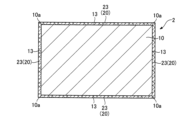
- Second Embodiment 3 is a cross-sectional view of a semiconductor device mounting board 2 according to the second embodiment.
- the semiconductor device mounting board 2 according to the second embodiment is different from the semiconductor device mounting board 1 according to the first embodiment (FIG. 1) in that the position at which the protective layer is disposed relative to the substrate is different.
- the semiconductor element mounting substrate 2 of the second embodiment includes a base material 10, a protective layer 20, an adhesion layer 30, an insulating layer 40, an adhesion layer 50, a bonding layer 60, an electrode 70, and a protective layer 80.
- a base material 10 a protective layer 20
- an adhesion layer 30 an insulating layer 40
- an adhesion layer 50 a bonding layer 60
- an electrode 70 an electrode 70
- a protective layer 80 a protective layer 80.
- the protective layer 20 covers the pair of main surfaces 11, 12 of the substrate 10 and the side surface 13 formed between the pair of main surfaces 11, 12.
- the protective layer 20 of the semiconductor element mounting board 2 has a protective layer 21 formed on one of the pair of main surfaces 11, 12, a protective layer 22 formed on the other main surface 12, and a protective layer 23 formed on the side surface 13. As shown in FIG. 3, the protective layer 23 is formed so as to connect to the protective layer 21 and the protective layer 22.
- the thickness of the protective layer 23 is smaller than the thickness of the substrate 10.
- FIG. 4 is a cross-sectional view taken along line A-A in FIG. 3, showing the substrate 10 and protective layer 23.
- the protective layer 23 is formed on each of the four side surfaces 13 of the substrate 10, which has a rectangular cross section perpendicular to the stacking direction of the layers in the semiconductor device mounting board 1.
- the four protective layers 23 are connected at each of the four corner portions 10a of the substrate 10, as shown in FIG. 4.
- the protective layer 23 is formed so as to cover the entire side surface 13 of the substrate 10.
- the protective layer 20 covers the entire surface of the substrate 10.
- the protective layer 20 disposed between the base material 10 and the electrode 70 is made of nickel, which has higher corrosion resistance to salt water than the copper that forms the base material 10. This makes it possible to suppress corrosion of the base material 10 due to the adhesion of salt water.
- the base material 10 formed in a flat plate shape has a pair of main surfaces 11, 12 and a side surface 13 formed between the pair of main surfaces 11, 12 covered by the protective layer 20. As a result, the surface of the base material 10 is not exposed, and corrosion of the base material 10 can be further suppressed.
- the semiconductor device mounting board supports the optical semiconductor and functions as a heat dissipation board that dissipates heat generated during light emission to the outside.
- the semiconductor device mounted on the semiconductor device mounting board is not limited to an optical semiconductor.
- the protective layer 20 is formed of nickel, which has higher corrosion resistance than copper forming the base material 10, for all of salt water, iodine potassium iodide solution, and hydrogen peroxide solution.
- the liquids to which the protective layer 20 is subject for corrosion resistance are not limited to these.
- the protective layer may be formed of a material that is more corrosion resistant than copper only to iodine potassium iodide solution, or may be formed of a material that is more corrosion resistant than the material forming the base material only to hydrogen peroxide solution.
- the protective layer may be gold, palladium, titanium, etc., which have a higher natural potential in iodine potassium iodide solution than copper, or may be gold, palladium, etc., which have a higher natural potential in hydrogen peroxide solution than copper.
- gold and palladium are both more corrosion resistant to salt water than copper, so if the protective layer is formed of gold or palladium, it is possible to suppress both corrosion due to adhesion of salt water during actual use and corrosion due to etching during the manufacture of the semiconductor element mounting substrate 1, as with the protective layer 20 of this embodiment.
- the natural potential of an object in an iodine potassium iodide solution or hydrogen peroxide solution can be determined by measuring the potential of the object immersed in the iodine potassium iodide solution or hydrogen peroxide solution.
- the protective layer 20 is formed on each of the pair of main surfaces 11, 12 of the substrate 10.
- the protective layer 20 covers the pair of main surfaces 11, 12 of the substrate 10 and the side surface 13 formed between the pair of main surfaces 11, 12.
- the position at which the protective layer 20 is formed on the substrate 10 is not limited thereto. It is sufficient that at least a portion of the protective layer 20 is disposed between the substrate 10 and the electrode 70.
- FIG. 5 is a schematic cross-sectional view of a modified example of the semiconductor element mounting substrate 1 of the first embodiment.
- the protective layer 20 has only a protective layer 21 formed on one of the main surfaces 11 on the side on which the insulating layer 40 and the electrodes 70 are formed.
- the semiconductor element mounting substrate 1 shown in FIG. 5 can also suppress corrosion of the base material 10 caused by salt water.
- the thickness of each of the protective layers 21, 22, and 23 of the protective layer 20 is smaller than the thickness of the base material 10.
- the thickness of each of the protective layers 21, 22, and 23 may be equal to or greater than the thickness of the base material 10. If the thickness of each of the protective layers 21, 22, and 23 is smaller than the thickness of the base material 10, when the semiconductor element mounting board 1 is used as a heat dissipation board for the semiconductor element 5a, the protective layers are unlikely to act as a resistance to heat dissipation, and therefore a decrease in the heat dissipation efficiency of the semiconductor element mounting board 1 can be suppressed.
- the protective layer 20 is formed of nickel, but the material forming the protective layer 20 is not limited to this.
- the protective layer 20 may be formed of a metal containing any one of nickel, gold, palladium, titanium, molybdenum, tungsten, platinum, silver, lead, and tin as a main component.
- the protective layer 20 may also be formed of a metal containing any one of a nickel-cobalt alloy (Ni-Co), a nickel-phosphorus alloy (Ni-P), and a nickel-boron alloy (Ni-B).
- the protective layer 20 may be formed of a material having higher corrosion resistance than the metal forming the base material 10.
- the base material 10 is made of copper.
- the material for forming the base material 10 is not limited to this.
- a metal having a relatively high thermal conductivity is preferable, but the material is not limited to metal.
- the semiconductor element mounting board includes an adhesion layer 30 that adheres the insulating layer 40 and the protective layer 20 to each other.
- the adhesion layer may not be provided.
- the material for forming the adhesion layer 30 is not limited to a metal mainly composed of titanium.
- the material for forming the adhesion layer 30 may be a metal mainly composed of chromium or molybdenum. Any material may be used as long as it adheres to both the protective layer 20 and the insulating layer 40.
- a semiconductor element mounting board A substrate made of a metal; An electrode connected to the semiconductor element; a protective layer disposed between the substrate and the electrode, the protective layer being made of a material having higher corrosion resistance than a metal forming the substrate;
- a semiconductor element mounting board comprising: (Application Example 2) The semiconductor element mounting board according to Application Example 1, The substrate is formed in a flat plate shape, The protective layer covers a pair of main surfaces of the base material and a side surface formed between the pair of main surfaces.
- a semiconductor element mounting board comprising: (Application Example 3) The semiconductor element mounting board according to the first or second aspect of the present invention, The thickness of the protective layer is smaller than the thickness of the base material.
- a semiconductor element mounting board comprising: (Application Example 4) The semiconductor element mounting board according to any one of Application Examples 1 to 3,
- the protective layer is formed of a metal containing any one of nickel, gold, palladium, titanium, molybdenum, tungsten, platinum, silver, lead, and tin as a main component.
- a semiconductor element mounting board comprising: (Application Example 5) The semiconductor element mounting board according to any one of Application Examples 1 to 4, further comprising: an insulating layer disposed between the substrate and the electrode; an adhesion layer disposed between the insulating layer and the protective layer and in close contact with each of the insulating layer and the protective layer;
- a semiconductor element mounting board comprising: (Application Example 6) The semiconductor element mounting board according to any one of Application Examples 1 to 5, The adhesion layer is formed of a metal containing any one of titanium, chromium, and molybdenum as a main component.
- a semiconductor element mounting board comprising:
Landscapes
- Engineering & Computer Science (AREA)
- Microelectronics & Electronic Packaging (AREA)
- Electrodes Of Semiconductors (AREA)
- Parts Printed On Printed Circuit Boards (AREA)
- Die Bonding (AREA)
Priority Applications (3)
| Application Number | Priority Date | Filing Date | Title |
|---|---|---|---|
| JP2025510652A JPWO2024203736A1 (https=) | 2023-03-30 | 2024-03-21 | |
| CN202480021466.1A CN120883361A (zh) | 2023-03-30 | 2024-03-21 | 半导体元件搭载用基板 |
| EP24779856.4A EP4693391A1 (en) | 2023-03-30 | 2024-03-21 | Substrate for mounting semiconductor element |
Applications Claiming Priority (2)
| Application Number | Priority Date | Filing Date | Title |
|---|---|---|---|
| JP2023055861 | 2023-03-30 | ||
| JP2023-055861 | 2023-03-30 |
Publications (1)
| Publication Number | Publication Date |
|---|---|
| WO2024203736A1 true WO2024203736A1 (ja) | 2024-10-03 |
Family
ID=92906084
Family Applications (1)
| Application Number | Title | Priority Date | Filing Date |
|---|---|---|---|
| PCT/JP2024/011069 Ceased WO2024203736A1 (ja) | 2023-03-30 | 2024-03-21 | 半導体素子搭載用基板 |
Country Status (4)
| Country | Link |
|---|---|
| EP (1) | EP4693391A1 (https=) |
| JP (1) | JPWO2024203736A1 (https=) |
| CN (1) | CN120883361A (https=) |
| WO (1) | WO2024203736A1 (https=) |
Citations (5)
| Publication number | Priority date | Publication date | Assignee | Title |
|---|---|---|---|---|
| JPH0629533A (ja) | 1992-07-10 | 1994-02-04 | Seiko Epson Corp | 半導体装置および、その製造方法 |
| JP2002368020A (ja) * | 2002-04-30 | 2002-12-20 | Sumitomo Electric Ind Ltd | サブマウントおよび半導体装置 |
| JP2004356429A (ja) * | 2003-05-29 | 2004-12-16 | Sumitomo Electric Ind Ltd | サブマウントおよびそれを用いた半導体装置 |
| JP2016029725A (ja) * | 2010-09-16 | 2016-03-03 | Shマテリアル株式会社 | 半導体発光素子搭載用基板、及びそれを用いた半導体発光装置 |
| WO2019082480A1 (ja) * | 2017-10-25 | 2019-05-02 | パナソニックIpマネジメント株式会社 | 光半導体装置用パッケージ、光半導体装置および光半導体装置用パッケージの製造方法 |
-
2024
- 2024-03-21 CN CN202480021466.1A patent/CN120883361A/zh active Pending
- 2024-03-21 EP EP24779856.4A patent/EP4693391A1/en active Pending
- 2024-03-21 JP JP2025510652A patent/JPWO2024203736A1/ja active Pending
- 2024-03-21 WO PCT/JP2024/011069 patent/WO2024203736A1/ja not_active Ceased
Patent Citations (5)
| Publication number | Priority date | Publication date | Assignee | Title |
|---|---|---|---|---|
| JPH0629533A (ja) | 1992-07-10 | 1994-02-04 | Seiko Epson Corp | 半導体装置および、その製造方法 |
| JP2002368020A (ja) * | 2002-04-30 | 2002-12-20 | Sumitomo Electric Ind Ltd | サブマウントおよび半導体装置 |
| JP2004356429A (ja) * | 2003-05-29 | 2004-12-16 | Sumitomo Electric Ind Ltd | サブマウントおよびそれを用いた半導体装置 |
| JP2016029725A (ja) * | 2010-09-16 | 2016-03-03 | Shマテリアル株式会社 | 半導体発光素子搭載用基板、及びそれを用いた半導体発光装置 |
| WO2019082480A1 (ja) * | 2017-10-25 | 2019-05-02 | パナソニックIpマネジメント株式会社 | 光半導体装置用パッケージ、光半導体装置および光半導体装置用パッケージの製造方法 |
Non-Patent Citations (1)
| Title |
|---|
| See also references of EP4693391A1 |
Also Published As
| Publication number | Publication date |
|---|---|
| CN120883361A (zh) | 2025-10-31 |
| JPWO2024203736A1 (https=) | 2024-10-03 |
| EP4693391A1 (en) | 2026-02-11 |
Similar Documents
| Publication | Publication Date | Title |
|---|---|---|
| US7518155B2 (en) | Light emitting element mounting member, and semiconductor device using the same | |
| JP4228303B2 (ja) | 半導体発光素子搭載部材と、それを用いた半導体発光装置 | |
| JP5864089B2 (ja) | 発光装置の製造方法 | |
| CN100583471C (zh) | 发光装置以及发光装置的制造方法 | |
| JP5073917B2 (ja) | 電気的なコンタクトを有する光電子半導体チップならびに該光電子半導体チップを製造するための方法 | |
| US7768028B2 (en) | Light emitting apparatus | |
| JP4763094B2 (ja) | 光半導体装置用リードフレーム及びその製造方法 | |
| JP2003258360A (ja) | サブマウントおよび半導体装置 | |
| WO2017006661A1 (ja) | セラミックス金属回路基板およびそれを用いた半導体装置 | |
| TWI499077B (zh) | 半導體發光元件 | |
| US11521912B2 (en) | Electronic element mounting substrate, electronic device, and electronic module | |
| JP2006093486A (ja) | 発光素子搭載用基板および発光装置 | |
| JP2006261569A (ja) | サブマウントおよびその製造方法 | |
| JP2008263248A (ja) | 半導体発光素子搭載部材およびその製造方法 | |
| WO2020071452A1 (ja) | 窓材、光学パッケージ | |
| WO2024203736A1 (ja) | 半導体素子搭載用基板 | |
| CN109768137B (zh) | 垂直结构led芯片及其制备方法 | |
| WO2024203737A1 (ja) | 半導体素子搭載用基板 | |
| JP2009194241A (ja) | 半導体素子搭載基板とそれを用いた半導体装置 | |
| JP7295778B2 (ja) | 波長変換部材、および、波長変換装置 | |
| KR20110004066A (ko) | 발광 장치 | |
| JP2024143277A (ja) | 半導体素子搭載用基板、および、半導体パッケージ | |
| JP5349416B2 (ja) | 発光素子搭載用基板および発光装置 | |
| JP2012059576A (ja) | 有機エレクトロルミネッセンス素子 | |
| JP2012138441A (ja) | Led用基板とその製造方法および半導体装置 |
Legal Events
| Date | Code | Title | Description |
|---|---|---|---|
| 121 | Ep: the epo has been informed by wipo that ep was designated in this application |
Ref document number: 24779856 Country of ref document: EP Kind code of ref document: A1 |
|
| ENP | Entry into the national phase |
Ref document number: 2025510652 Country of ref document: JP Kind code of ref document: A |
|
| WWE | Wipo information: entry into national phase |
Ref document number: 2025510652 Country of ref document: JP Ref document number: 202480021466.1 Country of ref document: CN |
|
| WWE | Wipo information: entry into national phase |
Ref document number: 2024779856 Country of ref document: EP |
|
| NENP | Non-entry into the national phase |
Ref country code: DE |
|
| WWP | Wipo information: published in national office |
Ref document number: 202480021466.1 Country of ref document: CN |
|
| ENP | Entry into the national phase |
Ref document number: 2024779856 Country of ref document: EP Effective date: 20251030 |
|
| ENP | Entry into the national phase |
Ref document number: 2024779856 Country of ref document: EP Effective date: 20251030 |
|
| ENP | Entry into the national phase |
Ref document number: 2024779856 Country of ref document: EP Effective date: 20251030 |
|
| ENP | Entry into the national phase |
Ref document number: 2024779856 Country of ref document: EP Effective date: 20251030 |
|
| ENP | Entry into the national phase |
Ref document number: 2024779856 Country of ref document: EP Effective date: 20251030 |
|
| ENP | Entry into the national phase |
Ref document number: 2024779856 Country of ref document: EP Effective date: 20251030 |
|
| ENP | Entry into the national phase |
Ref document number: 2024779856 Country of ref document: EP Effective date: 20251030 |
|
| ENP | Entry into the national phase |
Ref document number: 2024779856 Country of ref document: EP Effective date: 20251030 |
|
| WWP | Wipo information: published in national office |
Ref document number: 2024779856 Country of ref document: EP |