WO2024203435A1 - 転写用積層体の製造方法、転写用積層体および半導体装置の製造方法 - Google Patents
転写用積層体の製造方法、転写用積層体および半導体装置の製造方法 Download PDFInfo
- Publication number
- WO2024203435A1 WO2024203435A1 PCT/JP2024/010173 JP2024010173W WO2024203435A1 WO 2024203435 A1 WO2024203435 A1 WO 2024203435A1 JP 2024010173 W JP2024010173 W JP 2024010173W WO 2024203435 A1 WO2024203435 A1 WO 2024203435A1
- Authority
- WO
- WIPO (PCT)
- Prior art keywords
- substrate
- laminate
- film
- cured
- semiconductor element
- Prior art date
- Legal status (The legal status is an assumption and is not a legal conclusion. Google has not performed a legal analysis and makes no representation as to the accuracy of the status listed.)
- Ceased
Links
Images

Classifications
-
- H—ELECTRICITY
- H10—SEMICONDUCTOR DEVICES; ELECTRIC SOLID-STATE DEVICES NOT OTHERWISE PROVIDED FOR
- H10H—INORGANIC LIGHT-EMITTING SEMICONDUCTOR DEVICES HAVING POTENTIAL BARRIERS
- H10H29/00—Integrated devices, or assemblies of multiple devices, comprising at least one light-emitting semiconductor element covered by group H10H20/00
- H10H29/01—Manufacture or treatment
- H10H29/011—Manufacture or treatment of integrated devices comprising at least one light-emitting semiconductor component covered by group H10H20/00
-
- B—PERFORMING OPERATIONS; TRANSPORTING
- B23—MACHINE TOOLS; METAL-WORKING NOT OTHERWISE PROVIDED FOR
- B23K—SOLDERING OR UNSOLDERING; WELDING; CLADDING OR PLATING BY SOLDERING OR WELDING; CUTTING BY APPLYING HEAT LOCALLY, e.g. FLAME CUTTING; WORKING BY LASER BEAM
- B23K26/00—Working by laser beam, e.g. welding, cutting or boring
- B23K26/50—Working by transmitting the laser beam through or within the workpiece
- B23K26/57—Working by transmitting the laser beam through or within the workpiece the laser beam entering a face of the workpiece from which it is transmitted through the workpiece material to work on a different workpiece face, e.g. for effecting removal, fusion splicing, modifying or reforming
-
- H—ELECTRICITY
- H10—SEMICONDUCTOR DEVICES; ELECTRIC SOLID-STATE DEVICES NOT OTHERWISE PROVIDED FOR
- H10H—INORGANIC LIGHT-EMITTING SEMICONDUCTOR DEVICES HAVING POTENTIAL BARRIERS
- H10H29/00—Integrated devices, or assemblies of multiple devices, comprising at least one light-emitting semiconductor element covered by group H10H20/00
- H10H29/01—Manufacture or treatment
- H10H29/012—Manufacture or treatment of active-matrix LED displays
-
- H—ELECTRICITY
- H10—SEMICONDUCTOR DEVICES; ELECTRIC SOLID-STATE DEVICES NOT OTHERWISE PROVIDED FOR
- H10H—INORGANIC LIGHT-EMITTING SEMICONDUCTOR DEVICES HAVING POTENTIAL BARRIERS
- H10H29/00—Integrated devices, or assemblies of multiple devices, comprising at least one light-emitting semiconductor element covered by group H10H20/00
- H10H29/20—Assemblies of multiple devices comprising at least one light-emitting semiconductor device covered by group H10H20/00
- H10H29/24—Assemblies of multiple devices comprising at least one light-emitting semiconductor device covered by group H10H20/00 comprising multiple light-emitting semiconductor devices
-
- H—ELECTRICITY
- H10—SEMICONDUCTOR DEVICES; ELECTRIC SOLID-STATE DEVICES NOT OTHERWISE PROVIDED FOR
- H10P—GENERIC PROCESSES OR APPARATUS FOR THE MANUFACTURE OR TREATMENT OF DEVICES COVERED BY CLASS H10
- H10P72/00—Handling or holding of wafers, substrates or devices during manufacture or treatment thereof
- H10P72/30—Handling or holding of wafers, substrates or devices during manufacture or treatment thereof for conveying, e.g. between different workstations
-
- H—ELECTRICITY
- H10—SEMICONDUCTOR DEVICES; ELECTRIC SOLID-STATE DEVICES NOT OTHERWISE PROVIDED FOR
- H10W—GENERIC PACKAGES, INTERCONNECTIONS, CONNECTORS OR OTHER CONSTRUCTIONAL DETAILS OF DEVICES COVERED BY CLASS H10
- H10W72/00—Interconnections or connectors in packages
- H10W72/01—Manufacture or treatment
- H10W72/013—Manufacture or treatment of die-attach connectors
-
- H—ELECTRICITY
- H10—SEMICONDUCTOR DEVICES; ELECTRIC SOLID-STATE DEVICES NOT OTHERWISE PROVIDED FOR
- H10W—GENERIC PACKAGES, INTERCONNECTIONS, CONNECTORS OR OTHER CONSTRUCTIONAL DETAILS OF DEVICES COVERED BY CLASS H10
- H10W72/00—Interconnections or connectors in packages
- H10W72/071—Connecting or disconnecting
-
- H—ELECTRICITY
- H10—SEMICONDUCTOR DEVICES; ELECTRIC SOLID-STATE DEVICES NOT OTHERWISE PROVIDED FOR
- H10W—GENERIC PACKAGES, INTERCONNECTIONS, CONNECTORS OR OTHER CONSTRUCTIONAL DETAILS OF DEVICES COVERED BY CLASS H10
- H10W72/00—Interconnections or connectors in packages
- H10W72/071—Connecting or disconnecting
- H10W72/073—Connecting or disconnecting of die-attach connectors
-
- H—ELECTRICITY
- H10—SEMICONDUCTOR DEVICES; ELECTRIC SOLID-STATE DEVICES NOT OTHERWISE PROVIDED FOR
- H10W—GENERIC PACKAGES, INTERCONNECTIONS, CONNECTORS OR OTHER CONSTRUCTIONAL DETAILS OF DEVICES COVERED BY CLASS H10
- H10W90/00—Package configurations
-
- H—ELECTRICITY
- H10—SEMICONDUCTOR DEVICES; ELECTRIC SOLID-STATE DEVICES NOT OTHERWISE PROVIDED FOR
- H10W—GENERIC PACKAGES, INTERCONNECTIONS, CONNECTORS OR OTHER CONSTRUCTIONAL DETAILS OF DEVICES COVERED BY CLASS H10
- H10W95/00—Packaging processes not covered by the other groups of this subclass
Definitions
- the present invention relates to a method for manufacturing a transfer laminate, a transfer laminate, and a method for manufacturing a semiconductor device. More specifically, the present invention relates to a method for manufacturing a transfer laminate and a transfer laminate that are preferably used when mounting semiconductor elements using laser transfer technology, and further to a method for manufacturing a semiconductor device using the transfer laminate.
- LEDs light-emitting diodes
- micro-LEDs micro-LEDs
- a laser transfer technology As a method for mounting a large number of small semiconductor elements, a laser transfer technology has been proposed in which a laminate having an adhesive layer on a support substrate is prepared by mounting semiconductor elements on the side of the adhesive layer opposite the support substrate side, and then a laser is irradiated from the support substrate side of the transfer laminate to reduce the adhesive strength of the semiconductor elements, allowing the desired semiconductor elements to be transferred and mounted on another substrate such as a circuit board.
- This method has the advantage of being able to transfer semiconductor elements quickly and with high positional accuracy. Note that "transfer” refers to the movement of semiconductor elements from the original substrate to another substrate.
- the transfer laminate used in this laser transfer technology is a laminate in which the adhesive layer is ablated by laser irradiation, and the adhesive layer disappears from the transfer laminate, making it possible to transfer the target semiconductor element (for example, Patent Documents 1 to 3).
- Patent Document 1 describes a transfer laminate in which a support substrate and a semiconductor element are bonded with an adhesive layer containing 10% by mass or more of a laser light absorbing component that has absorption properties for the wavelength of laser light. It shows a method of transferring a semiconductor element by irradiating a laser from the support substrate side of the transfer laminate, and since an adhesive layer containing a laser light absorbing component is used in this case, the adhesive layer can be effectively ablated, allowing the semiconductor element to be transferred.
- ablation refers to the phenomenon in which a material decomposes, gasifies, and evaporates.
- Patent Document 2 describes a method for manufacturing a display using a transfer laminate in which a support substrate and a semiconductor element are bonded with an adhesive layer having a thickness of 0.1 ⁇ m or more and 0.5 ⁇ m or less.
- the method shows a method for transferring a semiconductor element by irradiating a laser from the support substrate side of the transfer laminate, and since a thin adhesive layer is used in this case, the adhesive layer can be completely removed by ablation, thereby preventing residual adhesive layer from remaining on the surface of the element after transfer.
- Patent Document 3 describes a transfer laminate that combines a support substrate and a semiconductor element, characterized in that the width of the adhesive layer on the surface that comes into contact with the support substrate is narrower than the width of the semiconductor element on the surface that comes into contact with the adhesive layer.
- the adhesive layer between adjacent semiconductor elements is not removed in the transfer laminate, so if the laser spot is misaligned and a laser is irradiated around the adhesive layer to which an element not to be transferred is fixed that is adjacent to the element to be transferred, the adhesive layer around the adjacent element may be ablated, and the adjacent element may be erroneously transferred.
- the adhesive layer between adjacent semiconductor elements is removed, but the method of removing the adhesive layer requires an etching process such as dry etching or wet etching after mounting a semiconductor element on the side of the adhesive layer opposite the support substrate side of the laminate having the adhesive layer on the support substrate, and therefore it takes time to prepare the transfer laminate.
- a transfer laminate for transferring a semiconductor element to another substrate comprising: (A) a light-transmitting substrate (first substrate); (B) a cured film obtained by curing a resin composition containing a curable resin; A substrate with a cured film having the above laminated thereon is then coated with the cured film. (C) a plurality of semiconductor elements having protruding electrodes; However, the protruding electrode portions are joined to the cured film in such a manner that the depth of the protruding electrode portions embedded in the cured film is equal to the height of the protruding electrode portions.
- the multiple semiconductor elements are not connected to adjacent semiconductor elements via a cured film, and the shortest distance between the protruding electrode portion and the first substrate is 0.1 ⁇ m or more and 1.0 ⁇ m or less.
- the transfer laminate described in [9] above, wherein the adhesive strength between the semiconductor element and a cured film obtained by curing the resin composition containing the curable resin (B) is 5 mN or more and 30 mN or less.
- a method for manufacturing a semiconductor device which uses a transfer laminate manufactured by the method for manufacturing a transfer laminate described in any one of [1] to [8] above, and includes a step of opposing a surface of the transfer laminate on which a semiconductor element is provided to a third substrate used for mounting the semiconductor element, and then irradiating a laser beam from the side of the first substrate of the transfer laminate to remove a cured film formed by curing a resin composition containing the curable resin, and transferring the semiconductor element to the third substrate.
- the method for manufacturing a laminate for transfer of the present invention does not require an etching process such as dry etching or wet etching, and even if the laser spot is misaligned during laser transfer, it is possible to obtain a laminate that is advantageous for laser transfer, in that it is possible to transfer only the desired semiconductor element with high precision without affecting adjacent elements.
- FIG. 13 is a diagram showing a method for confirming the degree of contact between the protruding electrode portion in the third laminate and a film formed by curing a resin composition containing a curable resin.
- FIG. 10 is a cross-sectional view showing a state in which a resin film between adjacent semiconductor elements has been removed in a transfer laminate whose surface is protected by a platinum film.
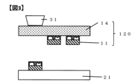
- FIG. 1A to 1C are diagrams showing an example of a laser transfer method using a transfer laminate.
- the method for producing the transfer laminate of the present invention includes the steps of: (1) A first laminate in which a resin composition containing a curable resin is laminated in an uncured film state on a first substrate having optical transparency; A step of preparing a second laminate on a second substrate having ultraviolet light transparency, the second laminate including a plurality of semiconductor elements each having at least one protruding electrode portion arranged such that the protruding electrode portion protrudes toward a side opposite to a front surface of the second substrate; (2) bonding the first laminate and the second laminate such that the surface on which the resin composition containing the curable resin is formed in a film form faces the surface on which the semiconductor element is disposed, thereby obtaining a third laminate; (3) curing the resin composition including the curable resin contained in the third laminate to form a cured resin film; (4) irradiating an ultraviolet laser from the side of the second substrate of the third laminate to separate the second substrate from the third laminate at an interface between the second substrate and the semiconductor element, and removing at least a part of the cured resin
- a first laminate is prepared in which a resin composition containing a curable resin is laminated in an uncured film state on a first substrate having optical transparency
- a second laminate is prepared in which a plurality of semiconductor elements having at least one protruding electrode portion are arranged on a second substrate having ultraviolet light transparency such that the protruding electrode portion protrudes toward the side opposite the surface of the second substrate.
- the first laminate can be produced by forming a resin composition containing a curable resin in an uncured film form on a first substrate that is optically transparent.
- a light-transmitting substrate is one that has an absorbance of 0.1 or less at any wavelength between 200 and 1100 nm.
- Substrates with such absorbance include inorganic substrates such as quartz, sapphire, alkali glass, non-alkali glass, and borosilicate glass.
- the thickness of the substrate can be selected within a range that does not impair the absorbance, and is preferably 0.1 mm to 5.0 mm. From the viewpoint of substrate handling, the thickness of the substrate is preferably 0.3 mm or more, and from the viewpoint of availability and versatility, the thickness of the substrate is more preferably 2.0 mm or less.
- the first substrate is a substrate that transmits the laser light used for irradiating the laser light from the side of the first substrate described later.
- the first substrate has the above-mentioned absorbance
- an organic substrate such as PET, aramid, polyester, polypropylene, or cycloolefin.
- the thickness of the substrate can be selected within a range that does not impair the above-mentioned absorbance, and is preferably 0.05 mm to 3.0 mm. From the viewpoint of handling the substrate, the thickness of the substrate is preferably 0.1 mm or more, and since light scattering during laser irradiation can be suppressed, the thickness of the substrate is more preferably 1.0 mm or less.
- the curable resin used in the resin composition refers to a resin that can change from an uncured state to a cured state by applying an external stimulus such as heating or irradiation with active energy rays, as the structure contained in the resin crosslinks.
- the uncured state of a resin composition containing a curable resin refers to a state in which the curing of the resin composition is not complete, and refers to a state in which the curing of the resin composition progresses further to a level described below at least by heating or irradiation with active energy rays.
- the resin composition is in an uncured state or not can be confirmed, for example, by immersing the first laminate in which the resin composition is formed into a film on the first substrate in a solvent, removing the resin composition from the first laminate, and whether the film thickness is 80% or less of the film thickness before immersion.
- the film thickness of the resin film in the first laminate does not decrease to 80% or less of the film thickness before immersion even when immersed in a solvent.
- the method of immersing the first laminate in a solvent is as follows: the first laminate is placed in a beaker large enough to allow the first laminate to be laid flat, and an amount of solvent that allows the first laminate to be immersed entirely (a solvent that can reduce the film thickness by 1 ⁇ m or more in at least a part of the region formed in a film shape when the resin composition containing the curable resin is completely uncured and immersed at 80 ° C for 5 minutes), and the first laminate is heated to 80 ° C and left to stand for 5 minutes, and then the first laminate is placed in a beaker containing the same solvent as the solvent used for immersion, which is prepared separately, and rinsed at room temperature for 1 minute.
- the first laminate is placed in a beaker containing isopropanol, and similarly rinsed at room temperature for 1 minute, and further the first laminate is placed in a beaker containing pure water and rinsed at room temperature for 1 minute. Finally, the first laminate is placed on a hot plate at 120 ° C and dried for 5 minutes, and the film thickness of the surface of the first laminate where the resin composition was applied in a film shape is measured with a contact step gauge, and it can be determined whether the film thickness is 80% or less of the film thickness before immersion.
- solvents that dissolve the uncured resin film include aprotic polar solvents such as ⁇ -butyrolactone and N-methyl-2-pyrrolidone, but it is also preferable to use the same solvent as that contained in the resin composition.
- the resin composition of the first laminate being in an uncured state makes it easy for the uncured resin composition to cover the entire surface of the protruding electrode portion of the semiconductor element of the second laminate in step (2) described below, and in this state, the adhesive strength between the semiconductor element and the cured resin film obtained by curing the uncured resin composition in step (3) described below can be increased. This prevents the semiconductor element from peeling off from the cured resin film due to the internal pressure of the decomposition gas generated when at least a portion of the cured resin film present between adjacent semiconductor elements is removed by irradiation with an ultraviolet laser in step (4) described below, and improves the mounting yield of semiconductor elements in the subsequent steps.
- An example of a method for forming the resin composition into a film on the first substrate is to coat the resin composition on the first substrate.
- Any coating method can be selected as the coating method, and examples include rotary coating using a spinner, spray coating, roll coating, and slit die coating.
- the resin composition is preferably dried for one minute to several tens of minutes at a temperature in the range of 50°C to less than 150°C using a hot plate, drying oven, or the like.
- the resin composition applied to the first substrate preferably has an absorbance of 0.4 or more and 5.0 or less in a film thickness of 1.0 ⁇ m at any wavelength of 200 to 380 nm, preferably the wavelength of an ultraviolet laser described below, in the form of a cured resin film. If the cured resin film satisfies the above absorbance, when the ultraviolet laser is irradiated to the third laminate in step (4) described below, the cured resin film efficiently absorbs the laser energy, and at least a portion of the cured resin film located between adjacent semiconductor elements is ablated and efficiently removed. Note that as long as the above absorbance is satisfied in the form of a cured resin film, the uncured resin composition formed into a film does not need to satisfy the above absorbance.
- the type of curable resin contained in the resin composition applied to the first substrate is not limited as long as the structure contained in the resin is crosslinked and changes from an uncured state to a cured state when an external stimulus such as heating or irradiation with active energy rays is applied, but examples include polyimide, polyimide precursor, polybenzoxazole, polybenzoxazole precursor, urethane resin, novolac resin, polyhydroxystyrene, polyester resin, acrylic resin, aramid resin, polysiloxane, and polyimidesiloxane.
- the curable resin contained in the resin composition applied to the first substrate preferably has a conjugated structure in its structure.
- a conjugated structure in its structure By having a conjugated structure in its structure, the absorbance of the cured resin film at any wavelength of 200 to 380 nm converted into a film thickness of 1.0 ⁇ m can be adjusted to a range of 0.4 to 5.0.
- structures having a conjugated structure include aromatic structures, and among them, structures such as biphenyl, imide, benzoxazole, and benzophenone are preferable.
- the above absorbance can be achieved by making 60 mol % or more of the monomer residues have a conjugated structure, when all the monomer residues constituting the resin are taken as 100 mol %. These resins may be contained alone or in a plurality of units in the resin film.
- the resin composition applied to the first substrate may contain additives such as ultraviolet absorbers, dyes, pigments, etc.
- additives such as ultraviolet absorbers, dyes, pigments, etc.
- the above absorbance can also be achieved by including additives such as ultraviolet absorbers, dyes, pigments, etc.
- additives that can be used include Tinuvin PS, Tinuvin 99-2, Tinuvin 326, Tinuvin 328, Tinuvin 384-2, Tinuvin 400, Tinuvin 405, Tinuvin 460, Tinuvin 477, Tinuvin 479, Tinuvin 900, Tinuvin 928, Tinuvin 1130 (the above are not limited to Tinuvin 1130).
- UV absorbers such as DAINSORB T-0, DAINSORB T-7, DAINSORB T-31, DAINSORB T-52, DAINSORB T-53, DAINSORB T-84, DAINSORB P-6, and DAINSORB P-7 (all trade names, manufactured by Daiwa Chemical Industry Co., Ltd.), Solvent Yellow 9
- the pigment include Solvent Yellow 3, Solvent Yellow 33, Solvent Orange 60, Solvent Red 111, Solvent Red 135, Solvent Red 168, Solvent Red 207, Solvent Red 52, Solvent Red 179, Solvent Blue 36, Solvent Blue 94, Solvent Blue 63, Solvent Blue 104, Solvent Blue 97, Solvent Green 20, Solvent Violet 13, Solvent Violet 36 (all trade names, manufactured by Tokyo Chemical Industry Co., Ltd.), carbon black, perylene black, cyanine black, aniline black, and other dyes, dyes, and pigments. These may be contained in the resin composition in one type or in multiple types.
- These compounds have high heat resistance and are therefore not easily decomposed by the heat applied when the uncured resin composition is heated and cured, or by the heat generated during the crosslinking reaction caused by irradiation with active energy rays.
- they since they have absorption at wavelengths in the range of 200 to 380 nm, they can be used to efficiently remove the resin film between the semiconductor elements by irradiating it with an ultraviolet laser in step (4) described below.
- the resin composition applied to the first substrate preferably has an indentation modulus of 1.0 GPa or more and 7.0 GPa or less at a depth of 20 to 40 nm from the surface of the resin film at 25°C when the curable resin is cured.
- the indentation modulus is a physical property that serves as an index for holding a semiconductor element in a resin film.
- the means for checking whether the resin is cured is as described above, but when a thermosetting resin is used as the curable resin, curing can usually be completed by heat treatment at 250°C for 30 minutes.
- indentation modulus of 1.0 GPa or more it is possible to prevent the semiconductor element from being displaced on the resin film due to the pressure of the gas generated when the cured resin film present between the semiconductor elements is removed by ablation during laser irradiation in step (4) described later. If the semiconductor element is displaced on the resin film, the distance between the adjacent semiconductor elements becomes shorter, and the laser hits not only the semiconductor element to be transferred but also the adjacent semiconductor elements during laser transfer, which may result in unintended transfer.
- indentation modulus of elasticity of 7.0 GPa or less peeling at the interface between the semiconductor element and the cured resin film can be more effectively prevented from occurring from the third laminate after curing in step (3) described below.
- the indentation modulus can be measured using a nanoindenter.
- the indentation modulus is measured by heating and curing the first laminate in step (1) at 250°C, and then using a Berkovich indenter (triangular pyramidal diamond indenter) to indent vertically from the surface of the resin film towards the first substrate at 25°C ⁇ 2°C in air, followed by unloading in an indentation load/unload test.
- the measurement is performed using a continuous stiffness measurement method at a measurement frequency of 100 Hz. From the obtained load-indentation depth diagram, the indentation modulus was calculated using the value at a depth of 20 to 40 nm from the resin film surface.
- the resin film contains flexible or bent components.
- the elastic modulus can be adjusted to a preferred range.
- components that increase flexibility or bendability include alkylene groups, aliphatic structures such as siloxane, or flexible structures derived from silane, alkylene glycol, flexible structures derived from ether groups such as biphenyl ether, alicyclic structures, and bent structures such as olefins.
- the elastic modulus can be made 7.0 GPa or less by containing 20 mol% or more of monomer residues having these structures that impart flexibility.
- the elastic modulus can be made 1.0 GPa or more by making it 70 mol% or less.
- the resin composition applied to the first substrate preferably contains a crosslinking agent.
- the addition of the crosslinking agent can partially crosslink the structure contained in the resin composition, thereby turning the uncured resin composition into a cured state.
- the type of crosslinking agent is not limited as long as it is a compound that undergoes a crosslinking reaction when heated at 100°C or higher and 300°C or lower, or a compound that undergoes a crosslinking reaction when irradiated with active energy rays, and examples of the crosslinking agent include compounds having functional groups such as epoxy groups, oxetanyl groups, alkoxymethyl groups, and methylol groups. Compounds having two or more of the functional groups per molecule are preferred, more preferably three or more, and even more preferably five or more. By having two or more of the functional groups per molecule, the crosslinking reaction can be efficiently generated when heated.
- crosslinking agents include compounds having an alkoxymethyl group or a methylol group, such as DML-PC, DML-PEP, DML-OC, DML-OEP, DML-34X, DML-PTBP, DML-PCHP, DML-OCHP, DML-PFP, DML-PSBP, DML-POP, DML-MBOC, DML-MBPC, DML-MTrisPC, DML-BisOC-Z, DMLBisOCHP-Z, DML-BPC, DML-BisOC-P, DMOM-PC, DMOM-PTBP, DMOM-MBPC, TriML-P, TriML-35XL, TML-HQ, TML-BP, TML- Examples include pp-BPF, TML-BPE, TML-BPA, TML-BPAF, TML-BPAP, TMOM-BP, TMOM-BPE, TMOM-BPA, TMOM-BPAF, TMOM-BPAP, H
- a crosslinking agent having an epoxy group examples include bisphenol A type epoxy resins, bisphenol F type epoxy resins, propylene glycol diglycidyl ether, polypropylene glycol diglycidyl ether, epoxy group-containing silicones such as polymethyl(glycidyloxypropyl)siloxane, and dimer acid-modified epoxy resins, but the present invention is not limited to these.
- Epicron 850-S Epicron HP-4032, Epicron HP-7200, Epicron HP-820, Epicron HP-4700, Epicron EXA-4710, Epicron HP-4770, Epicron EXA-859CRP, Epicron EXA-1514, Epicron EXA-4880, Epicron EXA-4850-150, Epicron EXA-4850-1000, Epicron EXA-4816, Epicron EXA-4822 (all trade names, manufactured by DIC Corporation), Rikaresin BEO-60E (hereinafter trade name, new Examples include Nippon Rika Co., Ltd.), EP-4003S, EP-4000S (all trade names, manufactured by Adeka Corporation), JER871, JER872, YX-4000, YX-4000H (all trade names, manufactured by Mitsubishi Chemical Corporation), Celoxide 2021P (all trade names, manufactured by Daicel Corporation), Showfree PETG, Showfree CDMGB, Showfree BATG (all trade names, manufactured by Resonac Corporation), Denacol
- a crosslinking agent having an oxetanyl group examples include OXT-121, OXT-221, OX-SQ-H, OXT-191, PNOX-1009, RSOX (all trade names, manufactured by Toagosei Co., Ltd.), "Ethanacol (registered trademark)” OXBP, and “Ethanacol” OXTP (all trade names, manufactured by UBE Co., Ltd.).
- the resin composition containing the curable resin may contain two or more types of crosslinking agents, and by containing preferably 0.1 parts by weight or more per 100 parts by weight of the total solid components of the resin composition, sufficient curability can be imparted. Furthermore, the crosslinking agent is preferably contained in an amount of 30 parts by weight or less per 100 parts by weight of the total solid components of the resin composition. If the crosslinking agent is contained in this range, the resin film after curing has a preferred range of elastic modulus.
- the resin composition applied to the first substrate may contain a photopolymerization initiator.
- a photopolymerization initiator By containing a photopolymerization initiator, the resin composition can be cured efficiently by irradiation with active energy rays.
- photopolymerization initiators include diethoxyacetophenone, 2-hydroxy-2-methyl-1-phenylpropan-1-one, benzyl dimethyl ketal, 1-(4-isopropylphenyl)-2-hydroxy-2-methylpropan-1-one, 4-(2-hydroxyethoxy)phenyl-(2-hydroxy-2-propyl)ketone, 1-hydroxycyclohexyl-phenyl ketone, 1-phenyl-1,2-propanedione-2-(o-ethoxycarbonyl)oxime, 2-methyl-[4-(methylthio)phenyl]-1,2-dione-2-(o-ethoxycarbonyl)oxime, and 2-methyl-[4-(methylthio)phenyl]
- the resin composition may contain two or more types of photopolymerization initiators, and the uncured resin composition can be cured by containing preferably 0.1 parts by weight or more per 100 parts by weight of the total solid components of the resin composition.
- the crosslinking agent is preferably contained in an amount of 30 parts by weight or less per 100 parts by weight of the total solid components of the resin composition. Within this range, sufficient curability can be imparted, and the resin film after curing has a preferred range of elastic modulus.
- the thickness of the film of the resin composition containing the curable resin formed on the first laminate is preferably selected from the range of 0.1 ⁇ m or more and 10 ⁇ m or less in an uncured state. As a lower limit, 0.3 ⁇ m or more is preferable, 0.5 ⁇ m or more is more preferable, and 0.7 ⁇ m or more is even more preferable.
- the uncured resin composition partially covers the protruding electrode portion of the semiconductor element, and the bonding strength between the cured resin film and the semiconductor element is increased by the curing of the film in the step (3) described later, and the semiconductor element can be prevented from being displaced on the resin film due to the pressure of the gas generated when the cured resin film between the semiconductor elements is removed by ablation during irradiation with an ultraviolet laser in the step (4) described later.
- the upper limit of the thickness of the resin composition containing the curable resin formed on the first laminate is preferably 3.0 ⁇ m or less, more preferably 2.0 ⁇ m or less, and even more preferably 1.5 ⁇ m or less.
- the resin composition containing the curable resin can be prevented from covering the side surface of the semiconductor layer of the semiconductor element beyond the area where the protruding electrode portion is present, and during irradiation with an ultraviolet laser in step (4) described below, the cured resin film present between the semiconductor elements can be efficiently removed and the semiconductor elements can be efficiently separated from the second substrate, improving the mounting yield of the semiconductor elements on the resin film.
- the 1% weight loss temperature when the curable resin contained in the resin composition applied to the first substrate is cured is preferably 300°C or higher. With a 1% weight loss temperature of 300°C or higher, the cured resin film (cured film) has high heat resistance, so that when the cured resin film present between the semiconductor elements is removed by ablation during the laser irradiation in step (4) described below, the cured resin film present between the semiconductor elements and the first substrate is removed in excess, preventing the semiconductor elements from peeling off from the first substrate. In addition, since the cured resin film present between the semiconductor elements is efficiently removed during the laser irradiation in step (4), the 1% weight loss temperature when the curable resin contained in the resin composition applied to the first substrate is cured is preferably 500°C or lower.
- the second laminate used in the present invention is a laminate in which a plurality of semiconductor elements having at least one protruding electrode portion are arranged on a second substrate having ultraviolet light transparency, the protruding electrode portion protruding toward the side opposite the surface of the second substrate.
- a substrate that is ultraviolet light transmissive refers to a substrate that has an absorbance of 0.1 or less at any wavelength between 200 and 380 nm.
- Substrates with such absorbance include inorganic substrates such as quartz, sapphire, alkali glass, non-alkali glass, and borosilicate glass.
- the thickness of the substrate can be selected within a range that does not impair the absorbance, and 0.1 mm to 5.0 mm is preferable. From the viewpoint of substrate handling, the thickness of the substrate is preferably 0.3 mm or more, and from the viewpoint of availability and versatility, the thickness of the substrate is more preferably 2.0 mm or less.
- the second substrate is a substrate that transmits the laser light used for irradiation of the ultraviolet laser from the side of the second substrate described later.
- the second substrate has the above-mentioned absorbance
- an organic substrate such as PET, aramid, polyester, polypropylene, or cycloolefin.
- the thickness of the substrate can be selected within a range that does not impair the above-mentioned absorbance, and is preferably 0.05 mm to 3.0 mm. From the viewpoint of handling the substrate, the thickness of the substrate is preferably 0.1 mm or more, and since light scattering during laser irradiation can be suppressed, the thickness of the substrate is more preferably 1.0 mm or less.
- the semiconductor element used in the present invention may be a semiconductor layer obtained by dicing semiconductors such as GaN, AlN, InN, InP, GaAs, Si, or SiC, and having at least one protruding electrode portion on one side directly or through another layer.
- These semiconductor elements also include those in which different types of semiconductor layers are further stacked, and those in which a sapphire substrate, glass substrate, wiring, etc. are stacked.
- light-emitting diodes (LEDs) are preferred in the present invention, and micro-LEDs are more preferred.
- the size of a micro-LED is, for example, 0.5 ⁇ m or more and 200 ⁇ m or less on one side.
- the height of a micro-LED is, for example, 0.5 ⁇ m or more and 200 ⁇ m or less, including the height of the protruding electrode portion.
- the protruding electrode portion is an electrode made of metal such as Au, In, Sb, Ag, Sn, or Pb, for connecting a semiconductor element to a circuit board or the like.
- the size of the protruding electrode portion is usually smaller than the size of the semiconductor element.
- the size of the protruding electrode portion of a micro LED is, for example, 0.2 ⁇ m or more and 100 ⁇ m or less on one side.
- the height of the protruding electrode portion of a micro LED is, for example, 0.1 ⁇ m or more and 50 ⁇ m or less.
- a plurality of semiconductor elements are arranged two-dimensionally on a second substrate having ultraviolet light transparency, for example, arranged in a lattice shape.
- each semiconductor element is fixed by a means that can be peeled off at the interface between the semiconductor element and the second substrate when irradiated with an ultraviolet laser.
- the plurality of semiconductor elements can be exemplified as being arranged in a lattice shape at regular intervals in the X-axis direction and the Y-axis direction.
- the number of the plurality of semiconductor elements arranged on the second substrate is preferably 5 pieces/cm 2 or more per unit area, more preferably 50 pieces/cm 2 or more.
- the number of the plurality of semiconductor elements arranged on the second substrate is preferably 500,000 pieces/cm 2 or less per unit area, more preferably 100,000 pieces/cm 2 or less.
- the distance between adjacent semiconductor elements is, for example, 0.1 ⁇ m or more and 200 ⁇ m or less.
- the second laminate may be one in which semiconductor elements are formed directly on a crystal growth substrate such as sapphire.
- a buffer layer may be provided at the interface between the crystal growth substrate and the semiconductor element.
- the second laminate may have another layer between the second substrate having ultraviolet light transparency and the semiconductor element.
- the semiconductor elements are arranged so that the protruding electrode portion protrudes toward the side opposite to the surface side of the second substrate.
- An example of the other layer is an adhesive layer.
- the adhesive layer preferably has an absorbance of 0.1 or less at a film thickness of 1.0 ⁇ m at any wavelength of 200 to 380 nm so as not to inhibit the removal of the resin film between adjacent semiconductor elements by irradiation with an ultraviolet laser in step (4) described later.
- peeling occurs at the interface between the second substrate and the semiconductor element, or at the interface between the semiconductor element and the other layer if there is another layer between the second substrate having ultraviolet light transparency and the semiconductor element.
- This phenomenon may occur when the other layer (e.g., the adhesive layer) itself is gasified and separated, or when a nitride film or the like present at the interface of the semiconductor element body (semiconductor layer) on the second substrate side is decomposed and separated.
- step (2) the first laminate and the second laminate are bonded together with the surface on which the resin composition containing the curable resin is formed in a film form facing the surface on which the semiconductor element is arranged, to obtain a third laminate.
- step (2) the first laminate and the second laminate are bonded together with the side on which the resin composition containing the curable resin is formed into a film facing the side on which the semiconductor element is arranged.
- Any method can be used for bonding as long as the bonding can be performed, but examples include a method in which the first laminate and the second laminate are bonded together using a bonding device that can control the pressure during bonding, such as a vacuum laminator, a wafer bonder, or a press machine, and such a method allows the first laminate and the second laminate to be bonded together uniformly.
- the pressure bonding conditions can be selected as long as the film of the resin composition containing the uncured curable resin comes into contact with the protruding electrode portion.
- the adhesive strength between the cured resin film and the semiconductor element is increased, and peeling at the interface between the cured resin film and the semiconductor element can be prevented after curing in step (3) or during irradiation with an ultraviolet laser in step (4) described below.
- the pressure during bonding is preferably 0.05 MPa or more so that the entire surface of the protruding electrode portion in contact with the uncured resin film is embedded in the uncured resin composition. Also, to prevent damage to the semiconductor element during bonding, it is preferable that the pressure be 10.0 MPa or less.
- the temperature during compression can be selected at will, but is preferably between 20°C and 100°C in order to maintain the resin film in an uncured state during compression.
- the compression time can be selected at will, but is preferably 5 seconds or more after the set pressure is reached in order to ensure sufficient adhesion. Also, it is preferably 30 minutes or less in order to shorten the processing time.
- the atmosphere during compression can be a vacuum, air, or an inert atmosphere.
- step (2) the protruding electrode portion is embedded in the film of the uncured resin composition, so that the uncured resin composition pushed out to the protruding electrode portion moves between the adjacent semiconductor elements, and the thickness of the film of the resin composition located between the semiconductor elements becomes thicker than in the state of the first laminate.
- Step (3) the resin composition containing the curable resin contained in the third laminate is cured to form a cured resin film.
- the resin composition in the third laminate is cured by heating or irradiating it with active energy rays to bring the uncured resin composition into a cured state.
- a hot plate, a drying oven, infrared rays, or the like can be used, and any temperature can be used as long as the uncured resin composition is cured without damaging the semiconductor element.
- a temperature of 100°C or higher can bring the uncured resin composition film into a cured state
- a temperature of 300°C or lower can prevent thermal decomposition that occurs with the curing of the resin composition film.
- the heating time can be any time that is sufficient to bring the uncured resin composition film into a cured state, and the appropriate time varies depending on the type of resin composition and the film thickness, but is preferably about 1 minute to several hours.
- the atmosphere during heating may be a vacuum, air, or an inert atmosphere.
- the third laminate it is a preferred embodiment to pressurize the third laminate so as to pressurize the gap between the first substrate and the second substrate during heating.
- the method of pressurization is preferably to apply pressure while heating using a pressure bonding device capable of controlling the pressure during pressure bonding, such as a vacuum laminator, a wafer bonder, or a press machine.
- the pressure for pressurization is arbitrary, but is preferably 0.05 MPa or more to counteract the effects of warping of the substrate. Also, to prevent damage to the semiconductor element during pressurization, it is preferably 10.0 MPa or less.
- the appropriate pressurization time varies depending on the type and film thickness of the resin film, but is preferably about 1 minute to several hours.
- the atmosphere during pressurization may be a vacuum, air, or an inert atmosphere.
- the same device can be used for steps (2) and (3), and the pressure on the third laminate can be left unreleased after step (2), and the curing process can be carried out in step (3).
- the pressure on the third laminate can be left unreleased after step (2), and the curing process can be carried out in step (3).
- peeling at the interface between the resin composition film and the semiconductor element in the third laminate due to warping of the substrate can be suppressed.
- the uncured resin composition is cured by irradiation with active energy rays
- an example is a method in which the third laminate is irradiated with active energy rays using an exposure device or the like.
- active energy rays that can be used in this case include ultraviolet rays, visible light, electron beams, and X-rays. Even in this case, it is preferable to cure the resin composition in the third laminate under pressure, and the method and conditions for applying pressure can be the same as those described above for curing by heating.
- the cured resin composition is preferably in contact with the entire surface of the protruding electrode portion.
- the degree to which the cured resin composition is in contact with the protruding electrode portion can be evaluated by the embedding depth of the protruding electrode portion into the cured resin film.
- the embedding depth corresponds to the height between the top and bottom where the electrode portion and the resin film are in contact, when the electrode portion side in contact with the resin film of the semiconductor element is the bottom and the semiconductor layer side is the top. In a state in which the cured resin is in contact with the entire surface of the protruding electrode portion, the embedding depth in the cured resin film will be the same as the height of the protruding electrode portion.
- the embedding depth in the cured resin film corresponds to the height (H ab ) between the top (H a ) and bottom (H b ) where the protruding electrode portion and the resin film are in contact, as shown in FIG. 1.
- the adhesion area between the semiconductor element and the resin film in the cured third laminate increases, increasing the adhesion strength, and preventing peeling of the interface between the semiconductor element and the resin film in the third laminate due to the pressure of decomposition gas generated by ablation of the cured resin composition film during irradiation with an ultraviolet laser in step (4) described below.
- the embedment depth can be measured from an image obtained by cutting out a cross section of the third laminate by focused ion beam (FIB) processing and observing it with a scanning electron microscope (SEM).
- the shrinkage rate of the resin composition film when it is changed from an uncured state to a cured state is preferably 0% or more and 10% or less.
- the resin film that covered the entire surface of the protruding electrode part in the uncured state can maintain the state of covering the entire surface of the protruding electrode part even after curing, and the embedment depth can be made to coincide with the height of the protruding electrode part.
- the shrinkage rate of the resin composition film when it is changed from an uncured state to a cured state is more preferably 0% or more and 5% or less, and even more preferably 0% or more and 3% or less.
- heat curing for example, the film thickness of the uncured resin composition of the first laminate in step (1) and the film thickness of the cured resin film after heat curing by heating the first laminate at 250 ° C. for 30 minutes are measured, and the shrinkage rate can be calculated from the reduction in film thickness.
- the thickness of the uncured resin composition of the first laminate in step (1) and the thickness of the cured resin film after irradiating the first laminate with an exposure dose of 1000 mJ/ cm2 for 10 minutes using a UV exposure machine are measured, and the thickness can be calculated from the amount of reduction in the thickness.
- step (4) an ultraviolet laser is irradiated from the second substrate side of the third laminate to separate the second substrate from the third laminate at the interface between the second substrate and the semiconductor element, and at least a part of the cured resin film present between the semiconductor elements is removed. Note that, in this case, removing at least a part means that a part of the cured resin film present between the semiconductor elements is exposed where no cured resin film is present between the first substrate and the second substrate.
- the ultraviolet laser is irradiated from the second substrate side of the third laminate to separate the second substrate from the third laminate at the interface between the second substrate and the semiconductor element.
- the type of laser and irradiation conditions of the ultraviolet laser used are not limited as long as it can separate the second substrate from the semiconductor element by gasifying the other layer (e.g., the adhesive layer) itself or by decomposing the nitride film present at the interface of the semiconductor element body (semiconductor layer) on the second substrate side.
- the laser wavelength is not limited as long as it is in the ultraviolet range (e.g., 200 to 380 nm), and examples of the wavelength include 248 nm, 266 nm, 308 nm, and 355 nm.
- Examples of the type of laser include solid lasers such as YAG laser, YVO 4 laser, fiber laser, and semiconductor laser, and gas lasers such as carbon dioxide laser, excimer laser, and argon laser, and can be selected according to the desired wavelength.
- the beam shape of the ultraviolet laser to be irradiated is not limited, and the spot size of the ultraviolet laser may be larger or smaller than the size of the semiconductor element. When the spot size is smaller than the size of the semiconductor element, the ultraviolet laser can be irradiated onto the entire area of the third laminate where the semiconductor element is bonded, while moving the spot.
- the energy density of the ultraviolet laser can be selected as long as it is sufficient energy for separating the semiconductor element from the second substrate.
- the energy density of the ultraviolet laser is preferably 100 mJ/cm 2 or more in order to sufficiently reduce the adhesive strength at the interface between the second substrate and the semiconductor element, and is preferably 2000 mJ/cm 2 or less in order to prevent damage to the semiconductor element.
- the number of scans of the laser irradiation may be one or more times as long as a part of the semiconductor element is decomposed at the interface between the second substrate and the semiconductor element, and the second substrate can be separated from the third laminate.
- the number of scans of the laser irradiation is preferably one or more times in order to sufficiently reduce the adhesive strength at the interface between the second substrate and the semiconductor element, and is preferably five or less in order to reduce the processing time. Three or less times is more preferable, two or less times is even more preferable, and one time is particularly preferable.
- the wavelength, energy density, and spot size may be changed each time.
- step (4) an ultraviolet laser is irradiated from the second substrate side of the third laminate to remove at least a portion of the cured resin film located between adjacent semiconductor elements.
- the resin film to which the semiconductor element to be transferred is fixed becomes more likely to be broken or lost due to ablation during subsequent laser transfer using the transfer laminate, and the energy density of the laser required for laser transfer can be reduced.
- step (4) it is preferable to remove the cured resin film present between adjacent semiconductor elements by irradiation with an ultraviolet laser, and divide the assembly of each semiconductor element and the cured resin film into cells (compartments). In other words, it is preferable to remove the resin film so that there is no cured resin film between the first substrate and the second substrate around the entire circumference of each semiconductor element. Since each semiconductor element is divided in a state of cells joined with the cured resin film, during the subsequent laser transfer using the transfer laminate, the resin film on which the semiconductor element to be transferred is fixed and the resin film on which the adjacent semiconductor element is fixed are not in contact with each other.
- the absorbance of the cured resin film at the wavelength of the ultraviolet laser converted to a film thickness of 1.0 ⁇ m is X
- the energy density of the ultraviolet laser is YmJ/cm 2
- the product of X and Y is 400 or more and 7,000 or less.
- the product of X and Y is 400 or more, the cured resin film located between adjacent semiconductor elements is easily removed, and the bonded body of each semiconductor element and the cured resin film can be divided into cells (partitions) with fewer laser irradiation scans.
- the product of X and Y is more preferably 450 or more.
- the product of X and Y is 7,000 or less, the positional deviation and peeling of the semiconductor element on the cured resin film can be suppressed.
- the product of X and Y is more preferably 6,500 or less, and even more preferably 5,500 or less.
- the sum of the values of the products of X and Y determined for the respective wavelengths is 400 or more and 7,000 or less.
- the width of the portion where the cured resin film is not present, which appears after the cured resin film is removed is preferably 1.0 ⁇ m or more.
- the width of the portion where the resin film is not present is equal to or smaller than the width between the protruding electrodes of the adjacent semiconductor elements.
- the width of the portion where the resin film is not present can be obtained by cutting out a cross section with an FIB over an area including the semiconductor element to be measured on the transfer laminate and the semiconductor element adjacent to that element, and observing it with an SEM.
- the area of the portion of the cell (partition) of the assembly of the semiconductor element and the cured resin film, which is partitioned by the portion where the cured resin film is not present, that contacts the second substrate may be larger or smaller than the area of the underside of the semiconductor element, and the area of the portion that contacts the second substrate is not particularly limited, but is preferably 50% or more of the area of the underside of the semiconductor element. By being 50% or more, the semiconductor element can be firmly held on the cured resin film. In addition, it is preferably 120% or less of the area of the underside of the semiconductor element. By being 120% or less, the distance between adjacent cells of the assembly of the semiconductor element and the cured resin film can be increased.
- the transfer laminate of the present invention can be obtained by the above-mentioned method for producing a transfer laminate, but the method for producing the transfer laminate is not limited to the above-mentioned method for producing a transfer laminate.
- the transfer laminate of the present invention is a transfer laminate in which (A) a substrate (first substrate) having optical transparency and (B) a cured film formed by curing a resin composition containing a curable resin are laminated to form a cured film-coated substrate, and (C) a plurality of semiconductor elements having protruding electrode portions are bonded to the substrate in a state in which the embedment depth of the protruding electrode portions in the cured film is equal to the height of the protruding electrode portions, and the plurality of semiconductor elements are not connected to adjacent semiconductor elements via the cured film, and the shortest distance between the protruding electrode portions and the first substrate is 0.1 ⁇ m or more and 1.0 ⁇ m or less.
- Examples of the curable resin used in the cured film formed by curing the resin composition containing the curable resin include the curable resin used in the resin composition applied to the first substrate described above.
- the cured film obtained by curing the resin composition containing the curable resin preferably has an absorbance of 0.4 or more and 5.0 or less at a wavelength of 200 to 1100 nm when converted into a film thickness of 1.0 ⁇ m.
- the absorbance is 0.4 or more
- the irradiated laser beam can be efficiently absorbed by the cured film.
- the lower limit of the absorbance is more preferably 0.6 or more, and since the absorption of the laser beam near the interface between the cured film and the first substrate having optical transparency can be particularly efficiently performed, transfer with even lower energy is possible.
- the upper limit of the absorbance is more preferably 5.0 or less, and since a versatile resin can be used, it is more preferably 4.0 or less.
- the curable resin used in the cured film obtained by curing the resin composition containing the curable resin preferably has a conjugated structure in its structure.
- the absorbance of the cured resin film at any wavelength of 200 to 1100 nm when converted into a film thickness of 1.0 ⁇ m can be adjusted to a range of 0.4 to 5.0.
- structures having a conjugated structure include aromatic structures, and among them, biphenyl, imide, benzoxazole, and benzophenone structures are preferable.
- the above absorbance can be achieved by making 60 mol % or more of the monomer residues having a conjugated structure when all the monomer residues constituting the resin are taken as 100 mol %.
- the curable resin having such a structure having a conjugated structure may be contained alone in the resin film, or may be contained in a mixture with other resins. It is preferable to use polyimide siloxane because it is easy to obtain the desired physical properties.
- the cured film obtained by curing the resin composition containing the curable resin (B) used in the present invention can achieve the above absorbance by including additives such as ultraviolet absorbers, dyes, dyes, and pigments in the resin film.
- additives included in the cured film include those described above as being included in the resin composition applied to the first substrate. These may be included alone or in combination in the cured film.
- the content of the additives in the cured film to achieve the above absorbance range is preferably 0.1 parts by weight or more per 100 parts by weight of the resin film obtained by curing the resin composition containing the curable resin (B), and preferably 50 parts by weight or less from the viewpoint of stability of the resin composition in the state before forming the laminate.
- the semiconductor elements are not connected to adjacent semiconductor elements via a cured film, i.e., there is no cured film between adjacent semiconductor elements around the entire periphery of each semiconductor element, during subsequent laser transfer using the transfer laminate, the cured film on which the semiconductor element to be transferred is fixed and the cured film on which the adjacent semiconductor element is fixed are not in contact, so that even if the position of the laser spot is shifted in any direction, it is possible to prevent the laser from hitting the cured film on which the adjacent semiconductor element not to be transferred is fixed, and it is possible to transfer only the desired semiconductor element and prevent the adjacent semiconductor element from being transferred.
- each semiconductor element by dividing each semiconductor element into cells that are joined to the cured film, if there is any cured resin film remaining between the elements, the semiconductor element will be transferred tilted due to the resistance generated when breaking the resin film between the elements during laser transfer, preventing a loss of accuracy.
- the transfer laminate of the present invention is bonded in a state where the embedment depth of the protruding electrode parts provided on the semiconductor element into the cured film matches the height of the protruding electrode parts.
- (C) multiple semiconductor elements having protruding electrode parts are firmly held to (B) the cured film formed by curing a resin composition containing a curable resin, improving the handleability of the transfer laminate.
- the shortest distance between the protruding electrode portion provided on the semiconductor element and the substrate is 0.1 ⁇ m or more and 1.0 ⁇ m or less.
- the pressure of the gas generated by ablation at the interface between (A) a light-transmitting substrate (first substrate) and (B) a cured film obtained by curing a resin composition containing a curable resin during laser transfer is efficiently transmitted to the semiconductor element, improving positional accuracy during laser transfer.
- the thickness of the cured film (B) located between the bottom of the protruding electrode portion and the substrate (A) can be measured from an image obtained by cutting a cross section of the transfer laminate by FIB processing and observing it with a SEM.
- the transfer laminate of the present invention preferably has an adhesive strength between the semiconductor element and a cured film formed by curing the resin composition containing the curable resin (B) of 5 mN or more and 30 mN or less.
- the adhesive strength is 5 mN or more, the semiconductor element is sufficiently held by the cured film, improving handling properties.
- the adhesive strength is 30 mN or less, the semiconductor element can be efficiently separated from the transfer laminate during laser transfer.
- the adhesive strength between the semiconductor element and the cured film can be measured using a die shear tester.
- the indentation modulus of the cured film formed by curing the resin composition containing the curable resin (B) at 25°C is 1.0 GPa or more and 7.0 GPa or less at a depth of 20 to 40 nm from the surface of the resin film.
- the semiconductor element is sufficiently held in the cured resin film, improving handling properties.
- the gas pressure caused by ablation generated at the interface between the first substrate and the cured film during laser transfer is efficiently propagated to the semiconductor element, allowing the semiconductor element to be transferred with high positional accuracy.
- the transfer laminate of the present invention may be prepared by a method other than the above-mentioned steps (1) to (4). Specifically, an example of the method is to irradiate the third laminate of step (3) with an ultraviolet laser from the second substrate side to separate the second substrate from the third laminate at the interface between the second substrate and the semiconductor element, and then remove the resin film between the semiconductor elements by wet etching or dry etching. Furthermore, when using a second laminate prepared by applying a substrate that can be removed by etching, such as GaAs, as the second substrate, an example of the method is to etch the hardened third laminate of step (3) to remove the second substrate, and then remove the resin film between the semiconductor elements by wet etching or dry etching.
- the method for manufacturing a semiconductor device using the transfer laminate of the present invention includes the steps of: placing the surface of the transfer laminate on which the semiconductor element is provided opposite a third substrate on which the semiconductor device is mounted; and then irradiating the transfer laminate with laser light from the side of the first substrate to remove the hardened resin film on the first substrate and transfer the semiconductor element to the third substrate.
- the third substrate can be any substrate, such as a glass substrate, a resin substrate, a metal substrate, or a circuit substrate on which wiring has already been formed.
- the third substrate may also have an adhesive layer to hold the semiconductor element after transfer.
- a material having adhesive properties such as polysiloxane resin, acrylic resin, polyester resin, or polyurethane resin, can be selected.
- the thickness of the adhesive layer is selected in the range of 0.5 ⁇ m to 100 ⁇ m depending on the size of the semiconductor element and the distance between the semiconductor element and the third substrate.
- a conductive bonding material such as an anisotropic conductive film (ACF), conductive silver paste, or solder may be formed on the wiring.
- the transfer laminate 120 and the third substrate 21 produced by the above-mentioned method are irradiated with laser light from a laser light irradiation device 31 from the first substrate side of the transfer laminate 120 toward the semiconductor element through the first substrate 14.
- the type of laser light includes solid lasers such as a YAG laser, a YVO4 laser, a fiber laser, and a semiconductor laser, and gas lasers such as a carbon dioxide laser, an excimer laser, and an argon laser, and can be selected depending on the wavelength to be used.
- the energy density of the laser light can be selected arbitrarily.
- the energy density of the laser light is preferably 1 mJ/cm2 or more , and from the viewpoint of preventing damage to the semiconductor element, it is preferably 2000 mJ/cm2 or less . More preferably, the energy density of the laser light is 10 mJ/ cm2 or more and 1000 mJ/cm2 or less.
- the transfer laminate of the present invention By using the transfer laminate of the present invention, even if the center of the laser spot is shifted from the center of the semiconductor element, the target semiconductor element can be transferred with high precision, and the transfer of adjacent semiconductor elements that are not the target of transfer can be prevented.
- the margin of the laser spot depends on the distance between the adjacent semiconductor elements, but it is preferable that the transfer can be performed with high precision even if the laser spot is shifted from the center of the semiconductor element by a range of 1 ⁇ m or more and 5 ⁇ m or less.
- the spot shape of the irradiated laser light is not limited, and it is preferable that the spot size is large enough to irradiate the entire cured film in contact with the semiconductor element to be transferred, but not large enough to reach the cured film in contact with the adjacent semiconductor element.
- the third substrate 21 it is also possible to heat the third substrate 21 when transferring the semiconductor element.
- an adhesive layer is formed on the third substrate, the retention of the transferred semiconductor element is improved.
- the semiconductor elements are transferred while adjusting the position to match the actual mounting location of the semiconductor elements in the semiconductor device to be fabricated.
- the LED elements are transferred to widen the spacing between them according to the LED pixel size and RGB arrangement.
- laser transfer is performed while moving the position of the transfer laminate or the third substrate to widen the spacing between the LED elements, by facing the semiconductor elements and the third substrate with a gap large enough to prevent contact between them, it is possible to prevent unintended transfer or peeling of the semiconductor elements due to contact.
- the shortest distance between the semiconductor elements and the surface of the third substrate is preferably 20 ⁇ m or more. In order to prevent a decrease in positional accuracy during laser transfer, it is preferable that the shortest distance between the semiconductor elements and the surface of the third substrate is 500 ⁇ m or less.
- the third substrate onto which the LED elements have been transferred is placed face-to-face with the circuit substrate and pressure-bonded to the circuit substrate to produce a circuit substrate on which the LED elements are mounted.
- the transfer can be performed with high positional accuracy, so the semiconductor elements can be transferred without misalignment with the circuit on the substrate on which they will ultimately be mounted, reducing mounting defects caused by misalignment.
- the laser light preferably has a wavelength of 248 nm, 266 nm, 308 nm, 355 nm, 532 nm, or 1064 nm, and it is particularly preferable to use a wavelength that has an absorbance of 0.4 or more when converted into a resin film with a thickness of 1.0 ⁇ m.
- semiconductor elements can be transferred with high precision.
- the laser light irradiated from the side of the first substrate is a laser light having a wavelength of 248 nm, 266 nm, or 355 nm, which allows accurate transfer of even minute semiconductor elements such as micro-LEDs. It is particularly preferable to use an excimer laser or a YAG laser as the laser light having a wavelength of 248 nm, 266 nm, or 355 nm.
- the third substrate is a circuit substrate. If the third substrate is a circuit substrate, the substrate transferred by the above method can be used as a semiconductor device as is. In addition, since there is no need to perform a transfer process from the third substrate to the circuit substrate in a later process, there is no concern about misalignment in the later process, and positional accuracy can be further improved.
- the circuit substrate a TFT substrate, a printed wiring substrate, or the like can be used.
- the transfer laminate (hereinafter referred to as "Laminate 4") was prepared by the method described in the first embodiment (Examples 1 to 24, Comparative Examples 1 to 3), the method described in the second embodiment (Example 25), or the method described in the third embodiment (Examples 26 and 27) described below.
- the refractive index used can be selected according to the type of resin in order to increase the accuracy of the measurement.
- Substrate (second substrate) having ultraviolet light transparency sapphire substrate (thickness 0.8 mm)
- Semiconductor element type GaN Size of semiconductor element: width 20.2 ⁇ m ⁇ length 30.3 ⁇ m ⁇ height 9.4 ⁇ m (height including protruding electrode part) Number of protruding electrodes: 2 on each surface. Size of protruding electrodes: 17.5 ⁇ m x 11.0 ⁇ m x 3.4 ⁇ m.
- Metal type of protruding electrode part Au Distance between adjacent elements: 10.0 ⁇ m in both width and length directions ⁇ Step (2)> Formation of a third laminate
- the first laminate prepared by the method of ⁇ Step (1)> (1)-1 described above was placed on the stage of a flip chip bonder (Toray Engineering, FC-3000WS) so that the film of the uncured resin composition was exposed on the surface, and the second laminate prepared by the method of ⁇ Step (1)> (1)-2 described above was placed on top of it so that the protruding electrode part of the second laminate was in contact with the film of the uncured resin composition provided on the first laminate. After applying a pressure of 0.5 MPa for 2 minutes, the pressure was released to form a third laminate.
- ⁇ Step (4)> Laser irradiation
- a varnish of a resin composition for forming a film of a resin composition containing a curable resin was applied using a spinner to a 6-inch quartz glass substrate with a thickness of 0.7 mm (manufactured by Corning, absorbance at 355 nm of 0.01 at a thickness of 0.7 mm; first substrate), and dried on a hot plate at 120°C for 3 minutes to prepare a first laminate in which a film of the resin composition containing an uncured curable resin was laminated.
- the refractive index used can be selected according to the type of resin in order to increase the accuracy of the measurement.
- (1)'-2 Preparation of second laminate A 4-inch LED substrate (with alignment marks) was prepared as the second laminate.
- the LEDs mounted are as follows. The size of the semiconductor element, the size of the protruding electrode portion, and the distance between adjacent elements were measured using a scanning electron microscope (S-4800, manufactured by Hitachi High-Technologies Corporation).
- Substrate (second substrate) having ultraviolet light transparency sapphire substrate (thickness 0.8 mm)
- Semiconductor element type GaN Size of semiconductor element: width 20.2 ⁇ m ⁇ length 30.3 ⁇ m ⁇ height 9.4 ⁇ m (height including protruding electrode part) Number of protruding electrodes: 2 on each surface. Size of protruding electrodes: 17.5 ⁇ m x 11.0 ⁇ m x 3.4 ⁇ m.
- Metal type of protruding electrode part Au Distance between adjacent elements: 10.0 ⁇ m in both width and length directions ⁇ Step (2)'> Formation of a third laminate
- the temperature of the stage plate and the upper pressure plate of a vacuum pressure device manufactured by Mikado Technos, VS08- ⁇ 300) was set to 80°C, and the first laminate prepared by the method of ⁇ Step (1)'> (1)-1 described above was placed on the stage plate of the vacuum pressure device so that the film of the uncured resin composition was exposed on the surface, and the second laminate prepared by the method of ⁇ Step (1)'> (1)-2 described above was placed on top of it so that the protruding electrode portion of the second laminate was in contact with the film of the uncured resin composition provided on the first laminate.
- ⁇ Step (4)'> Laser irradiation
- the third laminate produced by the method of ⁇ Step (3)'> above was irradiated with an ultraviolet laser from the second substrate side using a laser device (manufactured by Toray Engineering Co., Ltd.). After the entire surface of the second substrate was irradiated with the laser, the second substrate was separated from the third laminate to obtain the desired laminate (laminar body 4).
- the refractive index used can be selected according to the type of resin in order to increase the accuracy of the measurement.
- Substrate (second substrate) having ultraviolet light transparency sapphire substrate (thickness 0.8 mm)
- Semiconductor element type GaN Size of semiconductor element: width 20.2 ⁇ m ⁇ length 30.3 ⁇ m ⁇ height 9.4 ⁇ m (height including protruding electrode part) Number of protruding electrodes: 2 on each surface. Size of protruding electrodes: 17.5 ⁇ m x 11.0 ⁇ m x 3.4 ⁇ m.
- Metal type of protruding electrode part Au Distance between adjacent elements: 10.0 ⁇ m in both width and length directions ⁇ Step (2)"> Formation and curing of third laminate
- the temperature of the stage plate and the upper pressure plate of the vacuum pressure device manufactured by Mikado Technos, VS08- ⁇ 300) was set to 80°C, and the first laminate prepared by the method of ⁇ Step (1)"> (1)-1 described above was placed on the stage plate of the vacuum pressure device so that the film of the uncured resin composition was exposed on the surface, and the second laminate prepared by the method of ⁇ Step (1)"> (1)-2 described above was placed on top of it so that the protruding electrode part of the second laminate was in contact with the film of the uncured resin composition provided on the first laminate.
- the positions were adjusted so that the center of the surface of the opposing first laminate and the center of the surface of the second laminate coincided. Thereafter, a pressure of 1.5 kN was applied to the entire surfaces of the first substrate and the second substrate for 2 minutes, and the temperature of the stage plate and the upper pressure plate was raised to 250°C while maintaining the pressure, and maintained for 10 minutes after reaching 250°C, and then the pressure was released to heat-cure the film of the resin composition.
- ⁇ Step (4) Laser Irradiation
- the third laminate produced by the method of ⁇ Step (2)> above was irradiated with an ultraviolet laser from the second substrate side using a laser device (manufactured by Toray Engineering Co., Ltd.). After the entire surface of the second substrate was irradiated with the laser, the second substrate was separated from the third laminate to obtain the desired laminate (laminate 4).
- a first laminate for absorbance measurement was prepared by applying a film of a resin composition containing an uncured curable resin to a thickness of 0.5 to 1.5 ⁇ m in the same manner as in the above-mentioned ⁇ Step (1)> (1)-1.
- the first laminate for absorbance measurement prepared was heat-cured in an inert oven (manufactured by Koyo) at 250° C. for 30 minutes under air atmosphere.
- the absorbance of the resin film after heat curing was continuously measured from 200 nm to 400 nm using an ultraviolet-visible spectrophotometer (manufactured by Hitachi, Ltd., U-2910). From the obtained film, the absorbance at each wavelength of 248 nm, 266 nm, 308 nm, and 355 nm was read, and the absorbance per 1.0 ⁇ m of film thickness at each wavelength was calculated according to the following formula.
- the refractive index used can be selected according to the type of resin in order to increase the accuracy of the measurement.
- the mounting yield of the semiconductor elements mounted on the laminate 4 obtained by the first embodiment was determined by observing and photographing an area on the surface of the laminate 4 on which the semiconductor elements were mounted, the area being calculated from the size and spacing of the semiconductor elements to contain 5,000 semiconductor elements, counting the number of semiconductor elements actually mounted thereon, and calculating the ratio to 5,000.
- the mounting yield of the semiconductor elements mounted on the laminate 4 obtained in the second embodiment and the third embodiment was determined by observing and photographing the areas that should contain 5,000 semiconductor elements, calculated from the size and spacing of the semiconductor elements, at three locations in each of the three locations, the center of the laminate 4 and two locations 4.8 cm away from the center, with a digital microscope (Keyence Corporation, VHS-6000), counting the number of semiconductor elements actually mounted in each observation area, and calculating the ratio to 5,000. The average of the calculation results obtained at the three locations was determined.
- a dicing tape (UDT-1025MC, manufactured by Denka) was attached to the semiconductor element side of laminate 4, and the semiconductor element was peeled off to expose the cured resin film, creating a sample that was then cut to a size of approximately 10 mm x 10 mm.
- Measurement conditions Measurement environment: 25 ⁇ 2°C, atmospheric pressure Measurement frequency: 100Hz Measurement method: Continuous stiffness measurement method From the obtained load-indentation depth diagram, the elastic modulus was calculated from the average value of the values at a depth of 20 to 40 nm from the resin film surface.
- substrate 3 a substrate with an adhesive layer thickness of 5.0 ⁇ m
- Laser transfer was performed at a specified energy density. Transfer tests were performed on 10 semiconductor elements at each energy density.
- the amount of misalignment was calculated for each element that was successfully transferred to the substrate 3 using the method described above, and the positional accuracy was judged from the average value as follows: A misalignment of 0 ⁇ m or more and less than 2 ⁇ m was assigned a rating of "5", a rating of 2 ⁇ m or more and less than 3 ⁇ m was assigned a rating of "4", a rating of 3 ⁇ m or more and less than 4 ⁇ m was assigned a rating of "3”, a rating of 4 ⁇ m or more and less than 5 ⁇ m was assigned a rating of "2”, and a rating of 5 ⁇ m or more was assigned a rating of "1".
- PMDA Pyromellitic anhydride (manufactured by Daicel Corporation)
- BPDA 3,3',4,4'-biphenyltetracarboxylic anhydride (manufactured by Mitsubishi Chemical Corporation)
- BTDA 3,3',4,4'-benzophenonetetracarboxylic anhydride (manufactured by Fujifilm Wako Pure Chemical Industries, Ltd.)
- DIBOC di-tert-butyl dicarbonate (Tokyo Chemical Industry Co., Ltd.)
- PA Phthalic anhydride (Tokyo Chemical Industry Co., Ltd.)
- PDA p-phenylenediamine (Tokyo Chemical Industry Co., Ltd.)
- BAHF 4,4'-dihydroxy-3,3'-diaminophenylhexafluoropropane (Merck Co., Ltd.)
- APPS1 ⁇ , ⁇ -bis(3-aminopropyl)polydimethylsiloxane
- n the number of repetitions.
- NMP 2-methyl-1-pyrrolidone (manufactured by Mitsubishi Chemical Corporation)
- CHN Cyclohexanone (manufactured by Toyo Gosei Co., Ltd.)
- DMIB N,N-dimethylisobutyramide
- Tinuvin 477 hydroxyphenyltriazine-based ultraviolet absorber (manufactured by BASF Ltd.)
- TG-129 ⁇ -butyrolactone solution containing 19.9% by weight of a crosslinking agent having an alkoxymethyl group represented by the structure of formula (3) (manufactured by Sanwa Chemical Co., Ltd.)
- Production example 1 (curable resin: P-1) Into a reaction vessel equipped with a thermometer, a dry nitrogen inlet, a heating/cooling device using hot water/cooling water, and a stirrer, 233.92 g (0.27 mol) of APPS1, 26.35 g (0.017 mol) of APPS2, BAHF 18.68 g (0.051 mol) of PA was charged together with 189.5 g of CHN, and the mixture was stirred at 50° C. for 15 minutes to dissolve it. Then, 10.07 g (0.068 mol) of PA and 23.69 g of CHN were added, and the mixture was stirred at 60° C. The mixture was stirred for 15 minutes.
- Production example 5 (curable resin: P-5) Into a reaction vessel equipped with a thermometer, a dry nitrogen inlet, a heating/cooling device using hot water/cooling water, and a stirrer, 233.92 g (0.27 mol) of APPS1, 26.35 g (0.017 mol) of APPS2, BAHF 18.68 g (0.051 mol) of PA was charged together with 203.26 g of CHN, and the mixture was stirred at 50° C. for 15 minutes to dissolve it. Then, 2.01 g (0.014 mol) of PA and 25.41 g of CHN were added, and the mixture was stirred at 60° C. Stirred for 15 minutes.
- Example 25 Varnish 7 shown in Table 1 was prepared and filtered through a PTFE filter with a pore size of 0.1 ⁇ m. A first laminate was produced using this varnish by the method described in ⁇ Step (1)'> (1)-1. Furthermore, a second laminate was produced by the method described in ⁇ Step (1)'> (1)-2. Furthermore, each step was carried out as shown in ⁇ Step (2)'> to ⁇ Step (4)'>. Detailed conditions in each step and evaluation results are summarized in Tables 5 to 7.
- Varnish 7 shown in Table 1 was prepared and filtered through a PTFE filter with a pore size of 0.1 ⁇ m.
- a first laminate was produced using this varnish by the method described in ⁇ Step (1)"> (1)-1.
- a second laminate was produced by the method described in ⁇ Step (1)"> (1)-2.
- each step was carried out as described in ⁇ Step (2)"> and ⁇ Step (4)">. Detailed conditions and evaluation results for each step are summarized in Tables 5 to 7.
- H a is the uppermost part where the protruding electrode part and the resin film are in contact with each other.
- H b is the lowermost part where the protruding electrode part and the resin film are in contact with each other.
- H ab is the height between H a and H b.
Landscapes
- Engineering & Computer Science (AREA)
- Physics & Mathematics (AREA)
- Optics & Photonics (AREA)
- Chemical & Material Sciences (AREA)
- Chemical Kinetics & Catalysis (AREA)
- General Chemical & Material Sciences (AREA)
- Oil, Petroleum & Natural Gas (AREA)
- Plasma & Fusion (AREA)
- Mechanical Engineering (AREA)
- Laminated Bodies (AREA)
- Led Devices (AREA)
- Manufacturing & Machinery (AREA)
Priority Applications (3)
| Application Number | Priority Date | Filing Date | Title |
|---|---|---|---|
| KR1020257019919A KR20250165303A (ko) | 2023-03-29 | 2024-03-15 | 전사용 적층체의 제조 방법, 전사용 적층체 및 반도체 장치의 제조 방법 |
| CN202480009183.5A CN120584401A (zh) | 2023-03-29 | 2024-03-15 | 转印用层叠体的制造方法、转印用层叠体及半导体装置的制造方法 |
| JP2024518637A JPWO2024203435A1 (cg-RX-API-DMAC7.html) | 2023-03-29 | 2024-03-15 |
Applications Claiming Priority (2)
| Application Number | Priority Date | Filing Date | Title |
|---|---|---|---|
| JP2023-053075 | 2023-03-29 | ||
| JP2023053075 | 2023-03-29 |
Publications (1)
| Publication Number | Publication Date |
|---|---|
| WO2024203435A1 true WO2024203435A1 (ja) | 2024-10-03 |
Family
ID=92906072
Family Applications (1)
| Application Number | Title | Priority Date | Filing Date |
|---|---|---|---|
| PCT/JP2024/010173 Ceased WO2024203435A1 (ja) | 2023-03-29 | 2024-03-15 | 転写用積層体の製造方法、転写用積層体および半導体装置の製造方法 |
Country Status (5)
| Country | Link |
|---|---|
| JP (1) | JPWO2024203435A1 (cg-RX-API-DMAC7.html) |
| KR (1) | KR20250165303A (cg-RX-API-DMAC7.html) |
| CN (1) | CN120584401A (cg-RX-API-DMAC7.html) |
| TW (1) | TW202502563A (cg-RX-API-DMAC7.html) |
| WO (1) | WO2024203435A1 (cg-RX-API-DMAC7.html) |
Citations (7)
| Publication number | Priority date | Publication date | Assignee | Title |
|---|---|---|---|---|
| JP2014225569A (ja) * | 2013-05-16 | 2014-12-04 | ソニー株式会社 | 実装基板の製造方法、および電子機器の製造方法 |
| US20190181122A1 (en) * | 2017-12-13 | 2019-06-13 | Innolux Corporation | Electronic device and method of manufacturing the same |
| JP2019176154A (ja) * | 2018-03-28 | 2019-10-10 | 東レエンジニアリング株式会社 | 転写基板ならびにこれを用いた実装方法および画像表示装置の製造方法 |
| JP2021110875A (ja) * | 2020-01-14 | 2021-08-02 | 三星電子株式会社Samsung Electronics Co., Ltd. | ディスプレイ装置の製造方法、ディスプレイ装置、およびディスプレイ装置製造用中間体 |
| JP2022041533A (ja) * | 2020-09-01 | 2022-03-11 | 三星電子株式会社 | マイクロledディスプレイ製造用の中間構造体、マイクロledディスプレイ製造用中間構造体の製造方法、およびマイクロledディスプレイの製造方法 |
| CN115425122A (zh) * | 2022-09-15 | 2022-12-02 | 惠科股份有限公司 | Led芯片巨量转移方法及显示面板 |
| JP2023507820A (ja) * | 2019-12-18 | 2023-02-27 | ソウル バイオシス カンパニー リミテッド | マイクロledの転写方法およびマイクロledの転写装置 |
Family Cites Families (3)
| Publication number | Priority date | Publication date | Assignee | Title |
|---|---|---|---|---|
| JP6119335B2 (ja) | 2013-03-18 | 2017-04-26 | 日亜化学工業株式会社 | 発光素子保持構造体 |
| JP7321760B2 (ja) | 2019-05-09 | 2023-08-07 | 三星電子株式会社 | ディスプレイ装置の製造方法、およびソース基板構造体 |
| JPWO2022201767A1 (cg-RX-API-DMAC7.html) | 2021-03-26 | 2022-09-29 |
-
2024
- 2024-03-15 JP JP2024518637A patent/JPWO2024203435A1/ja active Pending
- 2024-03-15 CN CN202480009183.5A patent/CN120584401A/zh active Pending
- 2024-03-15 WO PCT/JP2024/010173 patent/WO2024203435A1/ja not_active Ceased
- 2024-03-15 KR KR1020257019919A patent/KR20250165303A/ko active Pending
- 2024-03-21 TW TW113110418A patent/TW202502563A/zh unknown
Patent Citations (7)
| Publication number | Priority date | Publication date | Assignee | Title |
|---|---|---|---|---|
| JP2014225569A (ja) * | 2013-05-16 | 2014-12-04 | ソニー株式会社 | 実装基板の製造方法、および電子機器の製造方法 |
| US20190181122A1 (en) * | 2017-12-13 | 2019-06-13 | Innolux Corporation | Electronic device and method of manufacturing the same |
| JP2019176154A (ja) * | 2018-03-28 | 2019-10-10 | 東レエンジニアリング株式会社 | 転写基板ならびにこれを用いた実装方法および画像表示装置の製造方法 |
| JP2023507820A (ja) * | 2019-12-18 | 2023-02-27 | ソウル バイオシス カンパニー リミテッド | マイクロledの転写方法およびマイクロledの転写装置 |
| JP2021110875A (ja) * | 2020-01-14 | 2021-08-02 | 三星電子株式会社Samsung Electronics Co., Ltd. | ディスプレイ装置の製造方法、ディスプレイ装置、およびディスプレイ装置製造用中間体 |
| JP2022041533A (ja) * | 2020-09-01 | 2022-03-11 | 三星電子株式会社 | マイクロledディスプレイ製造用の中間構造体、マイクロledディスプレイ製造用中間構造体の製造方法、およびマイクロledディスプレイの製造方法 |
| CN115425122A (zh) * | 2022-09-15 | 2022-12-02 | 惠科股份有限公司 | Led芯片巨量转移方法及显示面板 |
Also Published As
| Publication number | Publication date |
|---|---|
| JPWO2024203435A1 (cg-RX-API-DMAC7.html) | 2024-10-03 |
| TW202502563A (zh) | 2025-01-16 |
| KR20250165303A (ko) | 2025-11-25 |
| CN120584401A (zh) | 2025-09-02 |
Similar Documents
| Publication | Publication Date | Title |
|---|---|---|
| US9647242B2 (en) | Heat-conductive sealing member and electroluminescent element | |
| JP7790341B2 (ja) | 積層体および半導体装置の製造方法 | |
| JP5422878B2 (ja) | 半導体用接着組成物、それを用いた半導体装置および半導体装置の製造方法 | |
| JP2007211246A (ja) | 半導体用接着組成物、それを用いた半導体装置および半導体装置の製造方法 | |
| KR20150068442A (ko) | 플렉서블 디바이스용 기판, 플렉서블 디바이스 및 그 제조 방법, 적층체 및 그 제조 방법, 그리고 수지 조성물 | |
| JP2011222334A (ja) | 熱伝導性封止部材および素子 | |
| TWI654090B (zh) | 積層體及其處理方法暨可撓性裝置之製造方法 | |
| KR20160127032A (ko) | 폴리이미드 수지, 이것을 이용한 수지 조성물 및 적층 필름 | |
| WO2016076261A1 (ja) | 仮接着膜の製造方法、仮接着膜、積層体、デバイスウエハ付き積層体、仮接着用組成物 | |
| WO2011126083A1 (ja) | 熱伝導性封止部材およびそれにより封止された電子デバイス | |
| JP7806689B2 (ja) | 積層体、樹脂組成物、および半導体装置の製造方法 | |
| KR20170080715A (ko) | 적층체의 제조 방법, 기판의 처리 방법 및 적층체 | |
| JP5292793B2 (ja) | 半導体用接着シート、それを用いた半導体装置および半導体装置の製造方法 | |
| TW202502563A (zh) | 轉印用積層體的製造方法、轉印用積層體及半導體裝置的製造方法 | |
| JP2024139737A (ja) | 積層体および半導体装置の製造方法 | |
| TW201509242A (zh) | 透明電路基板之製造方法 | |
| JP2024139736A (ja) | 積層体および半導体装置の製造方法 | |
| CN121079761A (zh) | 层叠体、层叠体的制造方法、半导体装置的制造方法 | |
| WO2025164353A1 (ja) | 積層体、樹脂組成物および半導体素子付き積層体ならびにそれらを用いた半導体装置の製造方法 | |
| KR20250081193A (ko) | 반도체 공정용 필름 및 이의 제조 방법 | |
| JP2018140885A (ja) | ガラス積層体、電子デバイス作製用基板、及び電子デバイスの製造方法。 | |
| WO2023286429A1 (ja) | 回路基板の製造方法、離型フィルム付き回路基板前駆体、及び、無機基板付き回路基板前駆体 | |
| JP2008115241A (ja) | 半導体用接着組成物、それを用いた半導体装置および半導体装置の製造方法 | |
| KR20090112401A (ko) | 반도체 장치용 기판의 제조 방법 및 이에 의해 제조된반도체 장치용 기판 |
Legal Events
| Date | Code | Title | Description |
|---|---|---|---|
| WWE | Wipo information: entry into national phase |
Ref document number: 2024518637 Country of ref document: JP |
|
| 121 | Ep: the epo has been informed by wipo that ep was designated in this application |
Ref document number: 24779564 Country of ref document: EP Kind code of ref document: A1 |
|
| WWE | Wipo information: entry into national phase |
Ref document number: 202480009183.5 Country of ref document: CN |
|
| WWP | Wipo information: published in national office |
Ref document number: 202480009183.5 Country of ref document: CN |
|
| NENP | Non-entry into the national phase |
Ref country code: DE |
|
| 122 | Ep: pct application non-entry in european phase |
Ref document number: 24779564 Country of ref document: EP Kind code of ref document: A1 |