WO2024202031A1 - プリント配線板 - Google Patents
プリント配線板 Download PDFInfo
- Publication number
- WO2024202031A1 WO2024202031A1 PCT/JP2023/013622 JP2023013622W WO2024202031A1 WO 2024202031 A1 WO2024202031 A1 WO 2024202031A1 JP 2023013622 W JP2023013622 W JP 2023013622W WO 2024202031 A1 WO2024202031 A1 WO 2024202031A1
- Authority
- WO
- WIPO (PCT)
- Prior art keywords
- printed wiring
- wiring board
- insulating film
- conductive pattern
- opening
- Prior art date
- Legal status (The legal status is an assumption and is not a legal conclusion. Google has not performed a legal analysis and makes no representation as to the accuracy of the status listed.)
- Ceased
Links
Images


Classifications
-
- H—ELECTRICITY
- H05—ELECTRIC TECHNIQUES NOT OTHERWISE PROVIDED FOR
- H05K—PRINTED CIRCUITS; CASINGS OR CONSTRUCTIONAL DETAILS OF ELECTRIC APPARATUS; MANUFACTURE OF ASSEMBLAGES OF ELECTRICAL COMPONENTS
- H05K3/00—Apparatus or processes for manufacturing printed circuits
- H05K3/22—Secondary treatment of printed circuits
- H05K3/28—Applying non-metallic protective coatings
Definitions
- This disclosure relates to printed wiring boards.
- WO 2016/147993 Patent Document 1 describes a printed wiring board.
- the printed wiring board has a base film, a conductive pattern, and an insulating layer.
- the base film has a main surface.
- the conductive pattern is disposed on the main surface of the base film.
- the conductive pattern has a plurality of wiring portions arranged in a direction perpendicular to the normal to the main surface of the base film.
- the insulating layer is disposed on the main surface of the base film so as to cover the conductive pattern.
- the printed wiring board of the present disclosure comprises a base film having a principal surface, a conductive pattern disposed on the principal surface, and a coverlay having an adhesive layer disposed on the principal surface so as to cover the conductive pattern, and an insulating film disposed on the adhesive layer.
- the conductive pattern has a terminal portion.
- the coverlay has an opening that penetrates the coverlay and exposes the upper surface of the terminal portion. If the edge of the opening on the lower surface of the adhesive layer and the edge of the opening on the lower surface of the insulating film are respectively defined as a first opening edge and a second opening edge, the resin flow width, which is the distance between the first opening edge and the second opening edge, is 30 percent or less of the minimum width of the first opening edge.
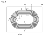
- FIG. 1 is a plan view of a printed wiring board 100.
- FIG. 2 is a bottom view of the printed wiring board 100.
- FIG. FIG. 3 is a cross-sectional view taken along line III-III in FIG.
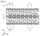
- FIG. 4 is a cross-sectional view taken along line IV-IV in FIG.
- FIG. 5 is a cross-sectional view taken along line VV in FIG.
- FIG. 6 is a cross-sectional view taken along line VI-VI in FIG. 7A to 7C are diagrams showing the manufacturing process of the printed wiring board 100.
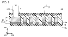
- FIG. 8 is a cross-sectional view of a printed wiring board 100 according to a modified example.
- the insulating layer may be, for example, a coverlay.
- the coverlay has an adhesive layer disposed on the main surface of the base film so as to cover the conductive pattern, and an insulating film disposed on the adhesive layer. To electrically connect the conductive pattern to the outside, the coverlay has an opening formed therein to expose the upper surface of the terminal portion of the conductive pattern.
- the edge of the opening on the underside of the adhesive layer is the first opening edge
- the edge of the opening on the underside of the insulating film is the second opening edge.
- This disclosure has been made in consideration of the problems with the conventional technology described above. More specifically, this disclosure provides a printed wiring board that can ensure the connection area of the terminal portion of the conductive pattern.
- the printed wiring board according to the embodiment includes a base film having a main surface, a conductive pattern disposed on the main surface, and a coverlay having an adhesive layer disposed on the main surface so as to cover the conductive pattern, and an insulating film disposed on the adhesive layer.
- the conductive pattern has a terminal portion.
- the coverlay has an opening that penetrates the coverlay and exposes the upper surface of the terminal portion. If the edge of the opening on the lower surface of the adhesive layer and the edge of the opening on the lower surface of the insulating film are respectively the first opening edge and the second opening edge, the resin flow width, which is the distance between the first opening edge and the second opening edge, is 30% or less of the minimum value of the width of the first opening edge.
- the resin flow width may be 0 mm or more and 0.3 mm or less.
- the thickness of the insulating film may be 2 ⁇ m or more and 7 ⁇ m or less. With the printed wiring board of (3) above, it is possible to further secure the connection area of the terminal portion.
- the thickness of the adhesive layer between the upper surface of the conductive pattern and the lower surface of the insulating film may be 3 ⁇ m or more and 15 ⁇ m or less.
- the thickness of the conductive pattern may be 30 ⁇ m or more and 150 ⁇ m or less.
- the conductive pattern may have a plurality of wiring portions.
- the normal to the main surface may be along a first direction.
- Each of the plurality of wiring portions may be along a second direction perpendicular to the first direction.
- the plurality of wiring portions may be arranged along a third direction perpendicular to the first direction and the second direction.
- the distance between two adjacent ones of the plurality of wiring portions may be 3 ⁇ m or more and 30 ⁇ m or less.
- the arithmetic mean height of the irregularities on the upper surface of the insulating film may be 0.010 ⁇ m or more and 1.00 ⁇ m or less.
- the conductive pattern may have a plurality of wiring parts.
- the normal to the main surface may be along a first direction.
- Each of the plurality of wiring parts may be along a second direction perpendicular to the first direction.
- the plurality of wiring parts may be arranged along a third direction perpendicular to the first direction and the second direction.
- the period of the projections and recesses on the upper surface of the insulating film may be 0.80 to 1.20 times the pitch between two adjacent ones of the plurality of wiring parts in the portion of the insulating film above the plurality of wiring parts.
- the insulating film may be made of polyimide or liquid crystal polymer.
- a printed wiring board according to the embodiment is referred to as a printed wiring board 100.
- FIG. 1 is a plan view of the printed wiring board 100.
- FIG. 2 is a bottom view of the printed wiring board 100.
- FIG. 2 shows the printed wiring board 100 as viewed from the opposite side to that of FIG. 1. Coverlays 31 and 32 are omitted from FIGS. 1 and 2.
- FIG. 3 is a cross-sectional view taken along III-III in FIG. 1.
- FIG. 4 is a cross-sectional view taken along IV-IV in FIG. 1.
- FIG. 5 is a cross-sectional view taken along V-V in FIG. 1.
- FIG. 6 is a cross-sectional view taken along VI-VI in FIG. 1.
- the printed wiring board 100 has a base film 10, conductive patterns 21 and 22, and coverlays 31 and 32.
- the base film 10 has a principal surface 10a and a principal surface 10b.
- the principal surface 10a and the principal surface 10b are end surfaces in the thickness direction of the base film 10.
- the principal surface 10b is the opposite surface to the principal surface 10a.
- the base film 10 is made of a flexible, electrically insulating material.
- the base film 10 is made of, for example, polyimide or liquid crystal polymer.
- the normal direction of the principal surface 10a (principal surface 10b) is defined as a first direction DR1.
- the conductive pattern 21 is disposed on the main surface 10a. When viewed in a plan view, the conductive pattern 21 is wound in a spiral shape. The conductive pattern 21 has a plurality of wiring portions 21a.
- the multiple wiring portions 21a may be multiple straight portions 21b or multiple curved portions 21c.
- the straight portions 21b extend linearly in a planar view.
- the curved portions 21c extend curvedly in a planar view.
- the extension direction of the wiring portions 21a (straight portions 21b, curved portions 21c) is defined as the second direction DR2. Note that when the wiring portions 21a are curved portions 21c, the second direction DR2 is the tangent direction of the curved portions 21c.
- the multiple wiring portions 21a are arranged at intervals along the third direction DR3.
- the third direction DR3 is perpendicular to the first direction DR1 and the second direction DR2.
- the conductive pattern 22 is disposed on the main surface 10b. When viewed in a plan view, the conductive pattern 22 is wound in a spiral shape.
- the conductive pattern 21 has a plurality of wiring portions 22a.
- the multiple wiring portions 22a may be multiple straight portions 22b or multiple curved portions 22c.
- the straight portions 22b extend linearly in a plan view.
- the curved portions 22c extend curvedly in a plan view.
- the wiring portions 22a (straight portions 22b, curved portions 22c) extend along the second direction DR2.
- the second direction DR2 is the tangent direction of the curved portions 22c.
- the multiple wiring portions 22a (straight portions 22b, curved portions 22c) are arranged at intervals along the third direction DR3.
- the conductive pattern 21 has a land 21d at one end and a land 21e at the other end. Lands 21d and 21e are located at the outermost and innermost circumferences of the conductive pattern 21, respectively.
- the conductive pattern 22 has a land 22d at one end and a land 22e at the other end. Lands 22d and 22e are located at the innermost and outermost circumferences of the conductive pattern 22, respectively. Lands 21d and 22e are terminal portions provided for electrical connection to the outside. Lands 21e and 22d overlap each other in a plan view.
- Each of the conductive patterns 21 and 22 is formed, for example, by a semi-additive method. More specifically, each of the conductive patterns 21 and 22 has a seed layer 23, an electroless plating layer 24, and an electrolytic plating layer 25. However, each of the conductive patterns 21 and 22 may also be formed by a subtractive method.
- the seed layer 23 is disposed on the main surface (main surface 10a, main surface 10b) of the base film 10.
- the seed layer 23 is, for example, a sputtered layer (a layer formed by sputtering).
- the seed layer 23 has, for example, a first layer and a second layer.
- the first layer is disposed on the main surface (main surface 10a, main surface 10b) of the base film 10.
- the second layer is disposed on the first layer.
- the first layer and the second layer are, for example, formed of a nickel-chromium alloy and copper, respectively.
- the electroless plating layer 24 is a layer formed by electroless plating.
- the electroless plating layer 24 is disposed on the seed layer 23.
- the electroless plating layer 24 is formed of, for example, copper.
- the electrolytic plating layer 25 is a layer formed by electrolytic plating.
- the electrolytic plating layer 25 is disposed on the electroless plating layer 24.
- the electrolytic plating layer 25 is formed of, for example, copper.
- a through hole 10c is formed in the base film 10.
- the through hole 10c penetrates the base film 10 in the thickness direction. In a plan view, the through hole 10c overlaps with the land 21e and the land 22d.
- the electroless plating layer 24 is also disposed on the inner wall surface of the through hole 10c.
- the electrolytic plating layer 25 is also embedded in the through hole 10c. This electrically connects the conductive pattern 21 and the conductive pattern 22 to each other. When a voltage is applied between the land 21d and the land 22e, a current flows in a spiral shape in the conductive pattern 21 and the conductive pattern 22, and a magnetic field is generated by this current. From another perspective, the printed wiring board 100 is a coil device.
- the thickness of the conductive pattern 21 is thickness T1.
- the thickness of the conductive pattern 22 is thickness T2.
- Thickness T1 and thickness T2 are, for example, 30 ⁇ m or more and 150 ⁇ m or less.
- the distance between two adjacent wiring portions 21a is distance DIS1.
- the distance between two adjacent wiring portions 22a is distance DIS2.
- Distance DIS1 and distance DIS2 are, for example, 3 ⁇ m or more and 30 ⁇ m or less.
- Each of the coverlays 31 and 32 has an adhesive layer 33 and an insulating film 34.
- the adhesive layer 33 is a layer formed from an adhesive.
- the adhesive layer 33 of the coverlay 31 is disposed on the main surface 10a so as to cover the conductive pattern 21.
- the adhesive layer 33 of the coverlay 32 is disposed on the main surface 10b so as to cover the conductive pattern 22.
- the insulating film 34 is disposed on the adhesive layer 33.
- the insulating film 34 is formed from, for example, polyimide or liquid crystal polymer.
- the thickness of the adhesive layer 33 of the coverlay 31 between the upper surface of the conductive pattern 21 and the lower surface of the insulating film 34 of the coverlay 31 is defined as thickness T3.
- the thickness of the adhesive layer 33 of the coverlay 32 between the upper surface of the conductive pattern 22 and the lower surface of the insulating film 34 of the coverlay 32 is defined as thickness T4.
- Thicknesses T3 and T4 are, for example, 3 ⁇ m or more and 15 ⁇ m or less.
- the thickness of the insulating film 34 of the coverlay 31 is defined as thickness T5.
- the thickness of the insulating film 34 of the coverlay 32 is defined as thickness T6.
- Thicknesses T5 and T6 are, for example, 2 ⁇ m or more and 7 ⁇ m or less.
- the arithmetic mean height (Sa) of the irregularities on the upper surface of the insulating film 34 is 0.010 ⁇ m or more and 1.00 ⁇ m or less.
- the arithmetic mean height of the irregularities on the upper surface of the insulating film 34 is measured using a laser microscope.
- the definition of the arithmetic mean height is as specified in ISO25178.
- the upper surface of the insulating film 34 has projections and recesses along the third direction DR3.
- the pitch between two adjacent wiring portions 21a is pitch P1.
- the pitch between two adjacent wiring portions 22a is pitch P2.
- the period of the projections and recesses on the upper surface of the insulating film 34 in the third direction DR3 is, for example, 0.80 to 1.20 times the pitch P1 on the portions of the insulating film 34 that are on the multiple wiring portions 21a.
- the period of the projections and recesses on the upper surface of the insulating film 34 in the third direction DR3 is, for example, 0.80 to 1.20 times the pitch P2 on the portions of the insulating film 34 that are on the multiple wiring portions 22a.
- the period of the unevenness on the top surface of the insulating film 34 in the third direction DR3 is obtained by measuring the top surface of the insulating film 34 with a laser microscope at a magnification of 20 times or more and 50 times or less, and measuring the distance between two adjacent convex portions.
- An opening 35 is formed in the coverlay 31.
- the opening 35 penetrates the coverlay 31 (adhesive layer 33 and insulating film 34) in the thickness direction.
- the upper surface of land 21d is exposed from opening 35.
- An opening 36 is formed in the coverlay 32.
- the opening 36 penetrates the coverlay 32 (adhesive layer 33 and insulating film 34) in the thickness direction.
- the upper surface of land 22e is exposed from opening 36.
- the width of the opening 35 in the insulating film 34 and the width of the opening 36 in the insulating film 34 are width W1 and width W2, respectively. Width W1 and width W2 are measured on the underside of the insulating film 34.
- Distance DIS3 is the distance between the edge of the opening 35 on the underside of the adhesive layer 33 and the edge of the opening 35 on the underside of the insulating film 34.
- Distance DIS4 is the distance between the edge of the opening 36 on the underside of the adhesive layer 33 and the edge of the opening 36 on the underside of the insulating film 34.
- Distance DIS3 and distance DIS4 correspond to the resin flow width. Note that width W1, width W2, distance DIS3, and distance DIS4 are measured by acquiring a planar image of the printed wiring board 100 using a microscope and based on the planar image.
- Distance DIS3 is 30 percent or less of the minimum value of width W1. In other words, the value obtained by dividing distance DIS3 by the minimum value of width W1 is 0.3 or less.
- Distance DIS4 is 30 percent or less of the minimum value of width W2. In other words, the value obtained by dividing distance DIS4 by the minimum value of width W2 is 0.30 or less.
- Distance DIS3 and distance DIS4 are, for example, 0 mm or more and 0.3 mm or less.
- FIG. 7 is a manufacturing process diagram of the printed wiring board 100. As shown in FIG. 7, the manufacturing method of the printed wiring board 100 includes a preparation process S1 and a coverlay attachment process S2. The coverlay attachment process S2 is performed after the preparation process S1.
- the base film 10, the coverlay 31, and the coverlay 32 are prepared. Note that in the base film 10 prepared in the preparation step S1, the conductive patterns 21 and 22 are arranged on the main surface 10a and the main surface 10b, respectively.
- the adhesive constituting the adhesive layer 33 is uncured.
- the openings 35 and 36 are formed, respectively, by, for example, a punching process.
- the coverlay 31 and the coverlay 32 are attached to the base film 10.
- the coverlay attachment process S2 first, the coverlay 31 is placed on the main surface 10a so that the adhesive layer 33 covers the conductive pattern 21, and the coverlay 32 is placed on the main surface 10b so that the adhesive layer 33 covers the conductive pattern 22.
- coverlays 31 and 32 are heat-pressed onto the base film 10.
- a cushioning material is interposed between the heat-pressing device and the coverlays 31 and 32. This causes the adhesive constituting the adhesive layer 33 to harden, and the coverlays 31 and 32 are attached to the base film 10.
- the cushioning material is made of a resin material.
- the glass transition point of the resin material constituting the cushioning material is lower than the heating temperature during the above-mentioned heat pressing. Therefore, during the above-mentioned heat pressing, the insulating film 34 deforms to conform to the shapes of the multiple wiring portions 21a (wiring portions 22a), and periodic unevenness is formed along the third direction DR3 on the upper surface of the insulating film 34 above the multiple wiring portions 21a (wiring portions 22a). In this way, a printed wiring board 100 having the structure shown in Figures 1 to 6 is formed.
- ⁇ Modification> 8 is a cross-sectional view of a modified printed wiring board 100. As shown in FIG. 8, the printed wiring board 100 does not have to have the conductive pattern 22 and the coverlay 32.
- the resin flow width is small. More specifically, in printed wiring board 100, distance DIS3 is 30 percent or less of the minimum value of width W1, and distance DIS4 is 1 percent or less of the minimum value of width W2. Therefore, in printed wiring board 100, the area of the top surface of lands 21d and 22d that are used for electrical connection to the outside is secured.
- thicknesses T5 and T6 are small, at 2 ⁇ m or more and 7 ⁇ m or less.
- a cushioning material that is easily softened (has a low glass transition point) is interposed between the heat press device and coverlays 31 and 32 when heat pressing is performed. Therefore, in printed wiring board 100, insulating film 34 is not easily deformed when heat pressing is performed, and increases in distances DIS3 and DIS4 due to resin flow are unlikely to occur.
- thicknesses T3 and T4 are large means that the pressure applied when the heat press is performed is small. The smaller the pressure applied when the heat press is performed, the less likely resin flow will occur, so the larger thicknesses T3 and T4 are, the easier it is to ensure the area of the upper surfaces of lands 21d and 22d that are used for electrical connection to the outside.
- the thinner the thicknesses T3 and T4 the closer the interface between the adhesive layer 33 and the insulating film 34 is to the neutral axis of the printed wiring board 100 when bent, making it easier to ensure adhesion between the adhesive layer 33 and the insulating film 34 when bent.
- the thicknesses T3 and T4 are 3 ⁇ m or more and 15 ⁇ m or less, it is possible to ensure adhesion between the adhesive layer 33 and the insulating film 34 while ensuring the area of the upper surfaces of the lands 21d and 22d that are used for electrical connection to the outside.
- Samples 1 to 72 were prepared to evaluate the relationship between thickness T1 (thickness T2), thickness T3 (thickness T4), thickness T5 (thickness T6) and distance DIS1 (distance DIS2) and distance DIS3 (distance DIS4). Details of Samples 1 to 72 are shown in Tables 1, 2, and 3. In Samples 1 to 72, the thickness T1, thickness T3, thickness T5, and distance DIS1 were changed, and then the distance DIS3 was measured. In Samples 1 to 72, the width W1 was constant at 0 ⁇ m.
- Condition A is that thickness T1 is 30 ⁇ m or more and 150 ⁇ m or less.
- Condition B is that thickness T3 is 3 ⁇ m or more and 15 ⁇ m or less.
- Condition C is that thickness T5 is 2 ⁇ m or more and 7 ⁇ m or less.
- Condition D is that distance DIS1 is 3 ⁇ m or more and 30 ⁇ m or less.
- the distance DIS3 was 0 mm or more and 0.3 mm or more (i.e., the distance DIS3 was 30 percent or less of the width W1).
- the distance DIS3 exceeded 0.3 mm.
Landscapes
- Engineering & Computer Science (AREA)
- Manufacturing & Machinery (AREA)
- Microelectronics & Electronic Packaging (AREA)
- Non-Metallic Protective Coatings For Printed Circuits (AREA)
Priority Applications (5)
| Application Number | Priority Date | Filing Date | Title |
|---|---|---|---|
| JP2024523460A JP7510029B1 (ja) | 2023-03-31 | 2023-03-31 | プリント配線板 |
| CN202380096422.0A CN120937508A (zh) | 2023-03-31 | 2023-03-31 | 印刷布线板 |
| PCT/JP2023/013622 WO2024202031A1 (ja) | 2023-03-31 | 2023-03-31 | プリント配線板 |
| TW113109927A TW202444146A (zh) | 2023-03-31 | 2024-03-18 | 印刷配線板 |
| JP2024098806A JP7754997B2 (ja) | 2023-03-31 | 2024-06-19 | プリント配線板 |
Applications Claiming Priority (1)
| Application Number | Priority Date | Filing Date | Title |
|---|---|---|---|
| PCT/JP2023/013622 WO2024202031A1 (ja) | 2023-03-31 | 2023-03-31 | プリント配線板 |
Publications (1)
| Publication Number | Publication Date |
|---|---|
| WO2024202031A1 true WO2024202031A1 (ja) | 2024-10-03 |
Family
ID=91671324
Family Applications (1)
| Application Number | Title | Priority Date | Filing Date |
|---|---|---|---|
| PCT/JP2023/013622 Ceased WO2024202031A1 (ja) | 2023-03-31 | 2023-03-31 | プリント配線板 |
Country Status (4)
| Country | Link |
|---|---|
| JP (2) | JP7510029B1 (https=) |
| CN (1) | CN120937508A (https=) |
| TW (1) | TW202444146A (https=) |
| WO (1) | WO2024202031A1 (https=) |
Families Citing this family (1)
| Publication number | Priority date | Publication date | Assignee | Title |
|---|---|---|---|---|
| CN120937508A (zh) * | 2023-03-31 | 2025-11-11 | 住友电工印刷电路株式会社 | 印刷布线板 |
Citations (6)
| Publication number | Priority date | Publication date | Assignee | Title |
|---|---|---|---|---|
| JP2006351676A (ja) * | 2005-06-14 | 2006-12-28 | Toray Ind Inc | カバーレイフィルムおよびそれを用いた複合配線板 |
| JP2007062175A (ja) * | 2005-08-31 | 2007-03-15 | Tokyo Tokushu Shigyo Kk | プレス成形用フィルム、プレス成形方法および回路板の製造方法 |
| JP2009238901A (ja) * | 2008-03-26 | 2009-10-15 | Toshiba Corp | フレキシブルプリント配線板および電子機器 |
| WO2020009229A1 (ja) * | 2018-07-06 | 2020-01-09 | タツタ電線株式会社 | プリント配線基板用貼付フィルム |
| WO2020196497A1 (ja) * | 2019-03-28 | 2020-10-01 | 三井化学東セロ株式会社 | プリント配線基板製造プロセス用離型フィルム、プリント基板の製造方法、プリント基板製造装置、及びプリント基板 |
| JP2022137124A (ja) * | 2020-11-10 | 2022-09-21 | 東亞合成株式会社 | 低誘電性接着剤組成物 |
Family Cites Families (9)
| Publication number | Priority date | Publication date | Assignee | Title |
|---|---|---|---|---|
| JPH0341960U (https=) * | 1989-09-01 | 1991-04-22 | ||
| US11083092B2 (en) * | 2015-03-13 | 2021-08-03 | Sumitomo Electric Printed Circuits, Inc. | Planar coil element and method for producing planar coil element |
| KR20170084672A (ko) * | 2016-01-12 | 2017-07-20 | 후지모리 고교 가부시키가이샤 | 커버레이 필름 |
| JP7509502B2 (ja) * | 2017-11-28 | 2024-07-02 | 住友電工プリントサーキット株式会社 | フレキシブルプリント配線板の製造方法及びフレキシブルプリント配線板 |
| JP7198190B2 (ja) * | 2019-10-04 | 2022-12-28 | 住友電気工業株式会社 | 接着剤組成物、フレキシブルプリント配線板用カバーレイ及びフレキシブルプリント配線板 |
| CN119899530A (zh) * | 2019-10-29 | 2025-04-29 | 日铁化学材料株式会社 | 聚酰亚胺组合物、树脂膜、层叠体、覆盖膜、带树脂的铜箔、覆金属层叠板及电路基板 |
| JP7357582B2 (ja) | 2020-04-20 | 2023-10-06 | 住友電気工業株式会社 | フレキシブルプリント配線板 |
| WO2022163284A1 (ja) | 2021-01-29 | 2022-08-04 | 信越ポリマー株式会社 | 接着剤組成物 |
| CN120937508A (zh) * | 2023-03-31 | 2025-11-11 | 住友电工印刷电路株式会社 | 印刷布线板 |
-
2023
- 2023-03-31 CN CN202380096422.0A patent/CN120937508A/zh active Pending
- 2023-03-31 WO PCT/JP2023/013622 patent/WO2024202031A1/ja not_active Ceased
- 2023-03-31 JP JP2024523460A patent/JP7510029B1/ja active Active
-
2024
- 2024-03-18 TW TW113109927A patent/TW202444146A/zh unknown
- 2024-06-19 JP JP2024098806A patent/JP7754997B2/ja active Active
Patent Citations (6)
| Publication number | Priority date | Publication date | Assignee | Title |
|---|---|---|---|---|
| JP2006351676A (ja) * | 2005-06-14 | 2006-12-28 | Toray Ind Inc | カバーレイフィルムおよびそれを用いた複合配線板 |
| JP2007062175A (ja) * | 2005-08-31 | 2007-03-15 | Tokyo Tokushu Shigyo Kk | プレス成形用フィルム、プレス成形方法および回路板の製造方法 |
| JP2009238901A (ja) * | 2008-03-26 | 2009-10-15 | Toshiba Corp | フレキシブルプリント配線板および電子機器 |
| WO2020009229A1 (ja) * | 2018-07-06 | 2020-01-09 | タツタ電線株式会社 | プリント配線基板用貼付フィルム |
| WO2020196497A1 (ja) * | 2019-03-28 | 2020-10-01 | 三井化学東セロ株式会社 | プリント配線基板製造プロセス用離型フィルム、プリント基板の製造方法、プリント基板製造装置、及びプリント基板 |
| JP2022137124A (ja) * | 2020-11-10 | 2022-09-21 | 東亞合成株式会社 | 低誘電性接着剤組成物 |
Also Published As
| Publication number | Publication date |
|---|---|
| TW202444146A (zh) | 2024-11-01 |
| JP7510029B1 (ja) | 2024-07-02 |
| CN120937508A (zh) | 2025-11-11 |
| JPWO2024202031A1 (https=) | 2024-10-03 |
| JP7754997B2 (ja) | 2025-10-15 |
| JP2024146952A (ja) | 2024-10-15 |
Similar Documents
| Publication | Publication Date | Title |
|---|---|---|
| US8015703B2 (en) | Method of manufacturing a wired circuit board | |
| US7971353B2 (en) | Production method of a wired circuit board | |
| CN101056498B (zh) | 布线电路基板集合体片 | |
| EP1675175B1 (en) | Wired circuit board | |
| CN102006716B (zh) | 布线电路基板及其制造方法 | |
| JP4865453B2 (ja) | 配線回路基板およびその製造方法 | |
| CN100586251C (zh) | 布线电路板 | |
| JP7754997B2 (ja) | プリント配線板 | |
| EP1906714A2 (en) | Wired Circuit Board and Producing Method Thereof | |
| US7407386B2 (en) | Wired circuit board and production method thereof | |
| JP4640815B2 (ja) | 配線回路基板集合体シートおよびその製造方法 | |
| KR20040078558A (ko) | 플렉시블 배선 회로 기판 | |
| CN1979673B (zh) | 配线电路基板及其制造方法 | |
| US11266024B2 (en) | Wired circuit board and production method thereof | |
| KR100470272B1 (ko) | 금속막 스크린마스크의 제조방법 | |
| JP4934101B2 (ja) | 配線回路基板の製造方法 | |
| WO2025089181A1 (ja) | コイル装置 | |
| WO2025089180A1 (ja) | コイル装置 | |
| CN120660452A (zh) | 印刷布线板 | |
| JP2005322946A (ja) | プリント配線板の製造方法及びプリント配線板 | |
| JP2006049587A (ja) | プリント配線板及びその製造方法 | |
| JP2006229155A (ja) | 配線回路基板 | |
| JP2006041178A (ja) | 配線基板及びその製造方法 | |
| JPH0632364B2 (ja) | 配線板の製造法 |
Legal Events
| Date | Code | Title | Description |
|---|---|---|---|
| WWE | Wipo information: entry into national phase |
Ref document number: 2024523460 Country of ref document: JP |
|
| 121 | Ep: the epo has been informed by wipo that ep was designated in this application |
Ref document number: 23930665 Country of ref document: EP Kind code of ref document: A1 |
|
| NENP | Non-entry into the national phase |
Ref country code: DE |
|
| 122 | Ep: pct application non-entry in european phase |
Ref document number: 23930665 Country of ref document: EP Kind code of ref document: A1 |