WO2024201629A1 - 半導体成長用テンプレート基板、半導体基板、半導体成長用テンプレート基板の製造方法および製造装置、並びに半導体基板の製造方法および製造装置 - Google Patents
半導体成長用テンプレート基板、半導体基板、半導体成長用テンプレート基板の製造方法および製造装置、並びに半導体基板の製造方法および製造装置 Download PDFInfo
- Publication number
- WO2024201629A1 WO2024201629A1 PCT/JP2023/012079 JP2023012079W WO2024201629A1 WO 2024201629 A1 WO2024201629 A1 WO 2024201629A1 JP 2023012079 W JP2023012079 W JP 2023012079W WO 2024201629 A1 WO2024201629 A1 WO 2024201629A1
- Authority
- WO
- WIPO (PCT)
- Prior art keywords
- semiconductor
- region
- substrate
- growth
- growth inhibition
- Prior art date
- Legal status (The legal status is an assumption and is not a legal conclusion. Google has not performed a legal analysis and makes no representation as to the accuracy of the status listed.)
- Ceased
Links
Images











Classifications
-
- H—ELECTRICITY
- H10—SEMICONDUCTOR DEVICES; ELECTRIC SOLID-STATE DEVICES NOT OTHERWISE PROVIDED FOR
- H10H—INORGANIC LIGHT-EMITTING SEMICONDUCTOR DEVICES HAVING POTENTIAL BARRIERS
- H10H20/00—Individual inorganic light-emitting semiconductor devices having potential barriers, e.g. light-emitting diodes [LED]
- H10H20/80—Constructional details
- H10H20/81—Bodies
- H10H20/822—Materials of the light-emitting regions
- H10H20/824—Materials of the light-emitting regions comprising only Group III-V materials, e.g. GaP
- H10H20/825—Materials of the light-emitting regions comprising only Group III-V materials, e.g. GaP containing nitrogen, e.g. GaN
-
- H—ELECTRICITY
- H10—SEMICONDUCTOR DEVICES; ELECTRIC SOLID-STATE DEVICES NOT OTHERWISE PROVIDED FOR
- H10P—GENERIC PROCESSES OR APPARATUS FOR THE MANUFACTURE OR TREATMENT OF DEVICES COVERED BY CLASS H10
- H10P14/00—Formation of materials, e.g. in the shape of layers or pillars
- H10P14/20—Formation of materials, e.g. in the shape of layers or pillars of semiconductor materials
-
- H—ELECTRICITY
- H10—SEMICONDUCTOR DEVICES; ELECTRIC SOLID-STATE DEVICES NOT OTHERWISE PROVIDED FOR
- H10P—GENERIC PROCESSES OR APPARATUS FOR THE MANUFACTURE OR TREATMENT OF DEVICES COVERED BY CLASS H10
- H10P14/00—Formation of materials, e.g. in the shape of layers or pillars
- H10P14/20—Formation of materials, e.g. in the shape of layers or pillars of semiconductor materials
- H10P14/29—Formation of materials, e.g. in the shape of layers or pillars of semiconductor materials characterised by the substrates
Definitions
- This disclosure relates to template substrates for semiconductor growth, etc.
- a mask pattern is formed on a base substrate including a heterogeneous substrate and a seed layer, on which a nitride semiconductor layer does not grow, and the nitride semiconductor layer is grown laterally on the mask portion, starting from the seed layer exposed in the opening where there is no mask portion, thereby reducing the defect density of the nitride semiconductor layer on the mask portion (Patent Document 1).
- the semiconductor growth template substrate disclosed herein comprises a main substrate and a base layer located above the main substrate and containing a base material, and the surface of the base layer includes a growth inhibition region in which the base material has been modified, and a seed region in which the base material has not been modified.
- FIG. 2 is a plan view showing a configuration of a template substrate according to the present embodiment.
- FIG. 2 is a cross-sectional view showing a configuration of a template substrate according to the present embodiment.
- 1 is a flowchart showing a method for manufacturing a template substrate according to the present embodiment.
- 1 is a block diagram showing a template substrate manufacturing apparatus according to an embodiment of the present invention.
- 1 is a flowchart showing a method for manufacturing a template substrate.
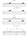
- 5A to 5C are cross-sectional views showing a method for manufacturing a template substrate.
- 5A to 5C are cross-sectional views showing a method for manufacturing a template substrate.
- 5A to 5C are cross-sectional views showing a method for manufacturing a template substrate.
- 5A to 5C are cross-sectional views showing a method for manufacturing a template substrate.
- FIG. 2 is a cross-sectional view showing a configuration of a template substrate according to the present embodiment.
- FIG. 2 is a cross-sectional view showing a configuration of a template substrate according to the present embodiment.
- FIG. 2 is a cross-sectional view showing a configuration of a template substrate according to the present embodiment.
- FIG. 2 is a cross-sectional view showing a configuration of a template substrate according to the present embodiment.
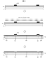
- 5A to 5C are cross-sectional views showing a method for manufacturing a template substrate.
- 5A to 5C are cross-sectional views showing a method for manufacturing a template substrate.
- 1 is a plan view showing a configuration of a semiconductor substrate according to an embodiment of the present invention.
- 1 is a cross-sectional view showing a configuration of a semiconductor substrate according to an embodiment of the present invention.
- 1 is a plan view showing a configuration of a semiconductor substrate according to an embodiment of the present invention.
- 1 is a cross-sectional view showing a configuration of a semiconductor substrate according to an embodiment of the present invention.
- 2 is a flowchart showing a method for manufacturing a semiconductor substrate according to the present embodiment.
- 1 is a block diagram showing a semiconductor substrate manufacturing apparatus according to an embodiment of the present invention; 2 is a flowchart showing a method for manufacturing a semiconductor substrate according to the present embodiment.
- 1A to 1C are cross-sectional views showing a method for manufacturing a semiconductor substrate according to an embodiment of the present invention.
- 1 is a cross-sectional view showing a configuration of a semiconductor substrate according to an embodiment of the present invention.
- 1 is a cross-sectional view showing a configuration of a semiconductor substrate according to an embodiment of the present invention.
- 1 is a cross-sectional view showing a configuration of a semiconductor substrate according to an embodiment of the present invention.
- 1A to 1C are plan views showing a method for manufacturing a semiconductor substrate according to an embodiment of the present invention.
- 1A to 1C are plan views illustrating a method for manufacturing a semiconductor substrate and a semiconductor device according to an embodiment of the present invention.
- 1A to 1C are plan views illustrating a method for manufacturing a semiconductor substrate and a semiconductor device according to an embodiment of the present invention.
- 1A to 1C are cross-sectional views showing a method for manufacturing a semiconductor substrate and a semiconductor device according to an embodiment of the present invention.
- 1 is a cross-sectional view showing an example of the configuration of an electronic device according to an embodiment of the present invention.
- 1 is a cross-sectional view showing an example of the configuration of an electronic device according to an embodiment of the present invention.
- FIG. 1 is a plan view showing the configuration of the template substrate according to this embodiment.
- FIG. 2 is a cross-sectional view showing the configuration of the template substrate according to this embodiment.
- the template substrate TS includes a main substrate 1 and an underlayer 4 located above the main substrate 1 and containing an underlayer material, and the surface of the underlayer 4 includes a growth inhibition region DA in which the underlayer material is modified and a seed region SA in which the underlayer material is not modified.
- the modification may be to change at least one of the contained elements and the crystal structure of the underlayer surface, and at least one of the contained elements and the crystal structure may be different between the growth inhibition region DA and the seed region SA.
- the growth inhibition region DA may be polycrystalline or amorphous.
- the growth inhibition region DA may have a larger occupancy rate of amorphous or polycrystalline than the seed region SA.
- the growth inhibition region DA may have a higher impurity concentration than the seed region SA, and this impurity concentration may be an oxygen concentration or an argon concentration. At least one element of oxygen (O), silicon (Si), and carbon (C) that is incorporated near the surface of the growth inhibition region DA (e.g., to a depth of about 0 to 5 nm) during the process of forming the growth inhibition region DA may enhance the growth inhibition function.
- O oxygen
- Si silicon
- C carbon
- the template substrate according to this embodiment does not include a mask pattern as in the conventional method, so that the semiconductor portion (e.g., nitride semiconductor crystal) is easily grown laterally (ELO) from above the seed area SA (the unmodified area on the surface of the underlayer 4) to above the growth inhibition area DA (the modified area on the surface of the underlayer 4), and a high-quality semiconductor portion (semiconductor layer) can be obtained.
- ELO laterally
- the impurities may segregate on the surface of the laterally grown semiconductor portion, making it difficult to form an upper layer film on the laterally grown semiconductor portion, and defects may occur at the interface with the upper layer film. If the film formation conditions for the lateral growth are restricted to avoid these problems, it may become difficult to form a semiconductor portion with a large aspect ratio (ratio of width to thickness), and the degree of freedom of the semiconductor portion shape for device design is reduced.
- a high-quality semiconductor portion e.g., nitride semiconductor crystal
- the aspect ratio of the semiconductor portion can be, for example, 5.0 or more, 10.0 or more, or 20.0 or more.
- the seed region SA may include a first region (first growth initiation region) S1 and a second region (second growth initiation region) S2, and the growth inhibition region DA may be located between the first region S1 and the second region S2.
- the first region S1 and the second region S2 may be arranged in a stripe pattern.
- the base material which is the main component of the base layer 4, may be a nitride semiconductor, and the main substrate 1 may be a heterogeneous substrate having a different lattice constant from the nitride semiconductor.
- the growth inhibition region DA and the seed region SA may be aligned in the a-axis direction of the nitride semiconductor.
- the width (length in the a-axis direction) of the growth inhibition region DA may be five times or more the width (length in the a-axis direction) of the first region S1.
- GaN-based semiconductors are semiconductors that contain gallium atoms (Ga) and nitrogen atoms (N), and typical examples include GaN, AlGaN, AlGaInN, and InGaN.
- the underlayer material may be, for example, aluminum nitride, and may include an aluminum layer (Al layer) between the main substrate 1 and the underlayer 4, which is an AlN layer.
- Al layer aluminum layer
- the heterogeneous substrate include a silicon substrate, a silicon carbide substrate, a sapphire substrate, an aluminum nitride substrate, and a ScAlMgO4 substrate.
- the underlayer material may be AlScN, ScN, ZnO, CrN, etc., including heterogeneous materials (e.g., metal elements other than group III elements) such as Sc (scandium), Zn, Cr, etc.
- the underlayer 4 may be a single layer structure or a multilayer structure. It may also be a multilayer structure including a periodic structure.
- FIG. 3 is a flowchart showing a method for manufacturing a template substrate according to this embodiment.
- the method for manufacturing a template substrate according to this embodiment includes a step S10 of forming an underlayer 4 containing an underlayer material (e.g., aluminum nitride) above a main substrate 1 (e.g., a silicon substrate), and a step S20 of forming a growth inhibition region DA obtained by subjecting the surface underlayer material to a modification treatment in the underlayer 4, and a seed region SA that has not been modified.
- FIG. 4 is a block diagram showing a template substrate manufacturing apparatus according to this embodiment.
- the template substrate manufacturing apparatus 30 includes an apparatus M10 that performs the step S10 in FIG. 3, an apparatus M20 that performs the step S20 in FIG. 3, and a control device M15 that controls the apparatus M10 and the apparatus M20.
- the apparatus M20 may be a modification treatment apparatus.
- FIG. 5 is a flowchart showing a method for manufacturing a template substrate.
- FIG. 6 is a cross-sectional view showing a method for manufacturing a template substrate.
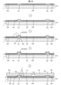
- step S20 following step S10 of forming an underlayer 4 containing an underlayer material may include step S22 of depositing a resist RZ on the underlayer 4, step S24 of patterning the resist RZ, step S26 of performing a plasma treatment on the exposed underlayer material, and step S28 of removing the resist RZ.
- the underlayer 4 may be formed by a sputtering method.
- argon plasma is irradiated onto the exposed surface 4D of the underlayer 4 to modify the surface of the irradiated area, forming a growth inhibition area DA.
- the plasma treatment can use oxygen plasma, nitrogen plasma, hydrogen plasma, or a mixture of these plasmas in addition to argon plasma.
- the growth inhibition area DA may contain argon, oxygen, nitrogen, etc. as impurities.
- the underlayer material may be aluminum nitride and the growth inhibition area DA may be aluminum oxynitride.
- the underlayer material may be AlScN (aluminum scandium nitride) and the growth inhibition area DA may be AlScON (aluminum scandium oxynitride).
- FIG. 7 is a cross-sectional view showing a method for manufacturing a template substrate. As shown in FIG. 7, the steps of patterning a resist RZ on an underlayer 4 (e.g., an AlN layer), forming a coating CM (e.g., a silicon nitride film of about 10 nm) covering the underlayer 4 and the resist RZ, removing the resist RZ (lift-off patterning of the coating CM), annealing the coating CM and the underlayer 4 (e.g., heating at 1000° C.), and removing the coating CM (e.g., removing the silicon nitride film by BHF) may be performed.
- a coating CM e.g., a silicon nitride film of about 10 nm
- a growth inhibition area DA located under the coating CM can be formed on the surface of the underlayer 4 due to the mutual diffusion phenomenon of the coating CM and the underlayer 4 during annealing.
- the surface under the coating CM can also be modified without undergoing an annealing process.
- the underlayer material may be AlScN, ScN, ZnO, CrN, etc., including a different material (e.g., a metal element other than group III) such as Sc (scandium), Zn, or Cr.
- the underlayer 4 may have a single layer structure or a multilayer structure. It may also have a multilayer structure including a periodic structure.
- FIG. 8 is a cross-sectional view showing a method for manufacturing a template substrate.
- a process of patterning and forming a resist RZ on an underlayer 4 e.g., an AlN layer
- a process of implanting impurity ions into the exposed underlayer material and a process of removing the resist RZ may be performed.
- impurities include Si (silicon), Fe (iron), and Mg (magnesium).
- impurity ions are embedded in the exposed surface 4D of the underlayer 4 to modify the surface and form a growth inhibition region DA.
- the underlayer material may be AlScN, ScN, ZnO, CrN, or the like, including a different material (e.g., a metal element other than group III) such as Sc (scandium), Zn, or Cr.
- the underlayer 4 may have a single layer structure or a multilayer structure. It may also have a multilayer structure including a periodic structure.
- FIG. 9 and 10 are cross-sectional views showing the configuration of the template substrate according to this embodiment.
- the growth inhibition region DA and the seed region SA may be flush with each other, or as shown in FIG. 9 and 10, the seed region SA (first and second regions S1 and S2) may be located above the growth inhibition region DA (planar region).
- the seed region SA first and second regions S1 and S2
- the growth inhibition region DA planar region
- the base layer 4 may be configured such that the portion including the first region S1 is thicker than the portion including the growth inhibition region DA, that is, the portion directly below the first region S1 (the portion overlapping the first region S1 in plan view) is thicker than the portion directly below the growth inhibition region DA (the portion overlapping the growth inhibition region DA in plan view).
- the main substrate 1 may have a convex portion Q protruding upward, and the first region S1 may be located on the convex portion Q.
- the underlayer material may be AlScN, ScN, ZnO, CrN, etc., including heterogeneous materials (e.g., metal elements other than group III elements) such as Sc (scandium), Zn, Cr, etc.
- the underlayer 4 may be a single layer structure or a multilayer structure. It may also be a multilayer structure including a periodic structure.
- the growth inhibition region DA formed by the surface modification process may have a thickness (t) that satisfies 0 ⁇ thickness (t) ⁇ 100 nm, or 0 ⁇ thickness (t) ⁇ 20 nm.
- the surface closer to the main substrate 1 (lower surface) may have a higher impurity concentration than the surface farther from the main substrate 1 (upper surface).
- FIG. 11 is a cross-sectional view showing the configuration of the template substrate according to this embodiment.
- the underlayer 4 may include a buffer layer 4B located on the main substrate 1 side and a seed layer 4S located on the surface side.
- a silicon substrate may be used as the main substrate 1, an Al layer as the buffer layer 4B, and an AlN layer as the seed layer 4S.
- a silicon substrate may be used as the main substrate 1, an AlN layer as the buffer layer 4B, and a GaN-based semiconductor layer as the seed layer 4S.
- FIG. 12 is a cross-sectional view showing the configuration of a template substrate according to this embodiment.
- the template substrate TS comprises a main substrate 1 and an underlayer 4 located on the main substrate 1, and includes a seed region SA located on the surface of the underlayer, and a growth inhibition region DA located on the surface of the main substrate and formed by modifying the main substrate material.
- the main substrate 1 may be a silicon substrate or a silicon carbide substrate.
- the growth inhibition region may include a silicon thermal oxide film.
- the main substrate 1 may be an AlN substrate or a sapphire substrate.
- FIG. 13 is a cross-sectional view showing a method for manufacturing a template substrate.
- a process may be performed in which an underlayer 4 (e.g., an AlN layer) is patterned on a main substrate 1 (e.g., a silicon substrate, a silicon carbide substrate) using, for example, a resist RZ, and a process may be performed in which the exposed surface of the main substrate is subjected to a thermal oxidation treatment.
- the underlayer 4 may be covered with the resist RZ during the thermal oxidation treatment.
- the exposed surface of the main substrate 1 is modified (oxidized) to form a thermal oxide film, and a growth inhibition region DA is formed.
- the growth inhibition region DA may be formed by performing a nitriding treatment instead of the thermal oxidation treatment.
- FIG. 14 is a cross-sectional view showing a method for manufacturing a template substrate.
- a step of patterning and forming an underlayer 4 e.g., an AlN layer, a GaN-based semiconductor layer
- a main substrate 1 e.g., a silicon carbide substrate, a sapphire substrate, an AlN substrate
- a plasma treatment on the exposed surface of the main substrate
- the exposed surface of the main substrate 1 is modified to form a growth inhibition region DA.
- the growth inhibition region DA may be formed by performing an implantation treatment of impurity ions.
- FIG. 15 is a plan view showing the configuration of the semiconductor substrate according to this embodiment.
- FIG. 16 is a cross-sectional view showing the configuration of the semiconductor substrate according to this embodiment.
- FIG. 17 is a plan view showing the configuration of the semiconductor substrate according to this embodiment.
- the semiconductor substrate 10 includes a template substrate TS having a growth inhibition region DA and a seed region SA (including the first and second regions S1 and S2) aligned in the first direction X1, and a first semiconductor portion 8A located above the template substrate TS and including a nitride semiconductor.
- the first semiconductor portion 8A includes a first raised portion R1 extending from the first region S1 to a position above the growth inhibition region DA (flat region), a first base portion B1 located above the first raised portion R1, and a first wing portion F1 connected to the first base portion B1, separated from the growth inhibition region DA, and located above the gap JD.
- the semiconductor substrate 10 may include a growth inhibition film 7 in contact with the first raised portion R1.
- the template substrate TS includes a main substrate 1 and an underlayer 4 located on the main substrate 1.
- the underlayer 4 may be made of a nitride semiconductor containing argon or oxygen as an impurity at 2 ⁇ 10 18 /cm 3 or more.
- the underlayer 4 can be formed by a sputtering method using argon gas.
- the direction from the main substrate 1 to the first semiconductor portion 8A is defined as "upward.” Viewing an object with a line of sight parallel to the normal direction of the semiconductor substrate 10 (including a see-through case) is sometimes called “planar view.”
- the first region S1, the first raised portion R1, and the first base portion B1 may overlap in a planar view, and the growth inhibition region DA and the first wing portion F1 may overlap in a planar view.
- the first wing portion F1 does not have to be in contact with the side of the first raised portion R1.
- the first semiconductor portion 8A contains a nitride semiconductor as a main component.
- the first semiconductor portion 8A may be doped (e.g., n-type containing a donor) or non-doped.
- a semiconductor substrate means a substrate containing a semiconductor, and the main substrate 1 of the template substrate TS may contain a semiconductor (e.g., silicon, silicon carbide) or may not contain a semiconductor.
- the first direction X1 may be the a-axis direction ( ⁇ 11-20> direction) of the first semiconductor portion 8A.
- the second direction X2 may be the m-axis direction ( ⁇ 1-100> direction) of the first semiconductor portion 8A (a nitride semiconductor such as GaN).
- the thickness direction of the first semiconductor portion 8A may be the c-axis direction ( ⁇ 0001> direction) of the first semiconductor portion 8A.
- the first semiconductor portion 8A may have two paired first wing portions F1 extending from the first base portion B1 in the first direction X1 and the opposite direction.
- the first semiconductor portion 8A can be formed by the ELO (Epitaxial Lateral Overgrowth) method, starting from the first protuberance R1 that grows from the first region S1.
- ELO Epiaxial Lateral Overgrowth
- the base portion B1 located above the first region S1 becomes a dislocation inheritance portion with many threading dislocations
- the first wing portion F1 located above the growth inhibition region DA becomes a low-defect portion with a lower threading dislocation density compared to the dislocation inheritance portion.
- the first raised portion R1 by forming the first raised portion R1, and forming the first wing portion F1 extending laterally (parallel to the first direction X1) from the first base portion B1 on the first raised portion R1 and positioned on the gap JD separated from the growth inhibition region DA, it is possible to form a wide first wing portion F1 with low defect density and high flatness.
- the first wing portion F1 may be entirely separated from the growth inhibition region DA. This allows the formation of a wide first wing portion F1 with low defect density and high flatness.
- ELO lateral overgrowth
- the semiconductor substrate 10 may include a second semiconductor portion 8C located above the template substrate TS.
- the template substrate TS has a second region S2 adjacent to the first region S1 via a growth inhibition region DA, and the second semiconductor portion 8C may have a second raised portion R2 extending from the second region S2 to a position above the growth inhibition region DA (flat region), a second base portion B2 located above the second raised portion R2, and a second wing portion F2 connected to the second base portion B2, separated from the growth inhibition region DA, and located above the gap JD.
- the first wing portion F1 and the second wing portion F2 may be aligned in the first direction X1 via a gap GP.
- first raised portion R1 and the second raised portion R2 may be collectively referred to as raised portion R
- first semiconductor portion 8A and the second semiconductor portion 8C may be collectively referred to as semiconductor portion 8
- the first wing portion F1 and the second wing portion F2 may be collectively referred to as wing portion F
- first base portion B1 and the second base portion B2 may be collectively referred to as base portion B.
- the growth inhibition film 7 may be in contact with the side surface RS of the first raised portion R1. This inhibits the growth of the semiconductor portion 8 from the side surface RS, making it easier to form the gap JD.
- the growth inhibition film 7 may be formed on at least a part of the side surface RS of the first raised portion R1, and may include a first film portion 7j in contact with the side surface RS of the first raised portion R1 and a second film portion 7i in contact with the upper surface RT of the first raised portion R1.
- the growth inhibition film 7 does not need to be a complete film, and may be a film containing one or more minute openings (a film with an incomplete shape).
- the second film portion 7i inhibits the threading dislocations propagated from the seed portion 3 to the first raised portion R1, and a new effect of improving the surface flatness and crystallinity of the first base portion B1 is obtained.
- the side surface RS of the first raised portion R1 may be a tapered surface that narrows upward. This allows the width of the gap JD facing the back surface of the first wing portion F1 to be wider than the width facing the growth inhibition area DA, making it possible to form a wide first wing portion F1 with fewer defects.
- the side surface RS which is a tapered surface, may intersect with the growth inhibition area DA.
- the growth inhibition film 7 may be in contact with the upper surface RT of the first raised portion R1.
- the second film portion 7i (the portion in contact with the upper surface RT of the first raised portion R1) located on the upper surface RT of the first raised portion R1 may be contained within the first semiconductor portion 8A. In this way, stress from the template substrate TS is alleviated.
- FIG. 18 is a cross-sectional view showing the configuration of a semiconductor substrate according to this embodiment. As shown in FIG. 18, a growth inhibition film 7 may be formed on the growth inhibition area DA.
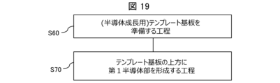
- FIG. 19 is a flowchart showing a method for manufacturing a semiconductor substrate according to this embodiment.
- the method for manufacturing a semiconductor substrate according to this embodiment includes a step S60 of preparing a template substrate for semiconductor growth, and a step S70 of forming a first semiconductor portion located above the template substrate.
- FIG. 20 is a block diagram showing an apparatus for manufacturing a semiconductor substrate according to this embodiment.
- the apparatus 80 for manufacturing a semiconductor substrate includes an apparatus M60 that performs step S60 in FIG. 19, an apparatus M70 that performs step S70 in FIG. 20, and a control device M65 that controls the apparatus M60 and the apparatus M70.
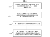
- the method for manufacturing a semiconductor substrate according to this embodiment includes a step S60 of preparing a template substrate TS including a seed region (first and second regions S1 and S2) and a growth inhibition region DA, a step S73 of forming a first raised portion R1 above the template substrate TS, the first raised portion R1 extending from the first region S1 to a position above the growth inhibition region DA, a step S75 of forming a growth inhibition film 7 in contact with the first raised portion R1, and a step S77 of forming a first base portion B1 located above the first raised portion R1 and a first wing portion F1 connected to the first base portion B1, separated from the growth inhibition region DA, and located above the gap JD.
- the first base B1 and the first wing F1 may be formed with the corner RC where the top surface RT and side surface RS of the first raised portion R1 intersect as the growth starting point PG.
- the corner RC may be used as the growth starting point PG, but is not limited to this.
- a defect e.g., a tiny opening
- the defect in the growth inhibition film 7 may be used as the growth starting point for the first base B1 and the first wing F1.
- the first protrusion R1, the growth suppression film 7, and the first base B1 and the first wing F1 may be continuously formed using an MOCVD apparatus.
- the first protrusion R1 may include a GaN-based semiconductor
- the growth suppression film 7 may be silicon nitride
- the first protrusion R1 may be formed by supplying a raw material serving as a gallium source (organic raw material such as trimethylgallium (TMG) or triethylgallium (TEG)) and a raw material serving as a nitrogen source (ammonia gas (NH 3 ))
- the growth suppression film 7 may be formed by stopping the supply of the raw material serving as a gallium source and supplying a silicon-based material (e.g., SiH 4 ) while maintaining the supply of the raw material serving as the nitrogen source.
- the first base B1 and the first wing F1 may include a GaN-based semiconductor, and the first base B1 and the first wing F1 may be formed by stopping the supply of the silicon-based material and supplying a raw material serving as a gallium source while maintaining the supply of the raw material serving as the nitrogen source. Also, the supply of a small amount of silicon-based material may be continued at a doping level.
- the film can be continuously deposited while forming the gap DJ under the wing portion F without removing it from the MOCVD apparatus, thereby reducing manufacturing time and costs.
- the gap DJ and forming the wing portion F so that it does not come into contact with the underlayer 4 (growth inhibition area DA), stresses from the main substrate 1 and underlayer 4 acting on the semiconductor portion 8 can be effectively alleviated.
- forming a gap under the wing portion may deteriorate the flatness of the underside of the wing portion (the surface facing the mask portion).
- burrs protrusions
- burrs may remain on both ends of the mask portion, and when these are overcome, the flatness of the underside of the semiconductor layer deteriorates.
- protrusions are less likely to occur because a growth inhibition area DA, which is a base modification layer, is formed, making it easier to flatten the underside of the wing portion F.
- the underside of the wing portion F is flat, since it can be used as a light extraction surface when forming a light-emitting device on the wing portion F, for example.
- the growth of the first wing portion F1 and the second wing portion F2 may be stopped before the first wing portion F1 and the second wing portion F2 growing toward the first wing portion F1 meet.
- the base layer 4 may be formed so that the portion including the first region S1 (the portion directly below the first region) is thicker than the portion including the growth inhibition region DA (the portion directly below the growth inhibition region).
- the main substrate 1 in the template substrate TS, may have a protrusion Q protruding upward, and the first region S1 may be formed on the protrusion Q.
- the first wing portion F1 of the first semiconductor portion 8A and the second wing portion F2 of the second semiconductor portion 8C may be in contact with the growth inhibition region DA.
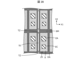
- FIGS. 26 and 29 are plan views showing the method for manufacturing a semiconductor substrate according to this embodiment.
- a functional layer (device layer) 9 may be formed on the first semiconductor portion 8A.
- the functional layer 9 of an LED, Laser, PD, Power device, etc. is formed using MOCVD, MBE, sputtering, etc.
- the active region (e.g., light-emitting region ES) of the functional layer 9 may be formed above the first wing portion F1 (device region), which is a low defect portion (low dislocation portion) (so as to overlap the first wing portion F1 in a plan view).
- electrodes EA and EC are formed on the functional layer 9, and predetermined portions of the first semiconductor portion 8A and the functional layer 9 are removed to separate the elements.
- a separation groove BM parallel to the first direction X1 is formed in the first semiconductor portion 8A and the functional layer 9, and the first semiconductor portion 8A and the functional layer 9 located on the first region S1 are removed leaving behind two paired tether portions TZ to form the element region PA.
- the two tether portions TZ are the portions of both ends of the element region PA facing each other in the second direction X2 that are connected to the first region S1.
- the element region PA (including the wing portion F, functional layer 9, and electrodes EA and EC) is separated from the template substrate TS to form a semiconductor device 25.
- a pressure member YS adheresive plate, adhesive sheet, adhesive substrate, etc.
- the two tapered portions TZ easily break and the semiconductor device 25 is separated from the template substrate TS.
- the semiconductor device 25 is peeled off from the template substrate TS while being held by the pressure member YS.
- the gap JD also functions effectively in element separation, allowing the semiconductor device 25 to be peeled off from the template substrate TS without damaging it.
- semiconductor devices 25 include light-emitting diodes (LEDs), semiconductor lasers, Schottky diodes, photodiodes, transistors (including power transistors and high electron mobility transistors), etc.
- LEDs light-emitting diodes
- semiconductor lasers semiconductor lasers
- Schottky diodes Schottky diodes
- photodiodes transistors (including power transistors and high electron mobility transistors), etc.
- FIG. 30 is a schematic diagram showing the configuration of an electronic device according to this embodiment.
- the electronic device 55 in FIG. 30 includes a semiconductor device 25 including a semiconductor portion 8, a drive substrate 23 on which the semiconductor device 25 is mounted, and a control circuit 27 that controls the drive substrate 23.
- FIG. 31 is a schematic diagram showing another configuration of the electronic device according to this embodiment.
- the element region (element portion) PA does not need to be peeled off from the template substrate TS.
- the electronic device 55 in FIG. 31 includes a semiconductor substrate 10 including the template substrate TS and the element region PA, a drive substrate 23 on which the semiconductor substrate 10 is mounted, and a control circuit 27 that controls the drive substrate 23.
- the main substrate included in the template substrate TS may be a light-transmitting substrate (e.g., a sapphire substrate).
- the electronic device 55 include a light-emitting device, a display device, a laser emission device (including a Fabry-Perot type and a surface emission type), a measuring device, a lighting device, a communication device, an information processing device, and a power control device.
Priority Applications (4)
| Application Number | Priority Date | Filing Date | Title |
|---|---|---|---|
| PCT/JP2023/012079 WO2024201629A1 (ja) | 2023-03-27 | 2023-03-27 | 半導体成長用テンプレート基板、半導体基板、半導体成長用テンプレート基板の製造方法および製造装置、並びに半導体基板の製造方法および製造装置 |
| JP2025511048A JPWO2024204391A1 (https=) | 2023-03-27 | 2024-03-27 | |
| PCT/JP2024/012324 WO2024204391A1 (ja) | 2023-03-27 | 2024-03-27 | 半導体基板、および半導体基板の製造方法 |
| CN202480020914.6A CN120958553A (zh) | 2023-03-27 | 2024-03-27 | 半导体基板以及半导体基板的制造方法 |
Applications Claiming Priority (1)
| Application Number | Priority Date | Filing Date | Title |
|---|---|---|---|
| PCT/JP2023/012079 WO2024201629A1 (ja) | 2023-03-27 | 2023-03-27 | 半導体成長用テンプレート基板、半導体基板、半導体成長用テンプレート基板の製造方法および製造装置、並びに半導体基板の製造方法および製造装置 |
Publications (1)
| Publication Number | Publication Date |
|---|---|
| WO2024201629A1 true WO2024201629A1 (ja) | 2024-10-03 |
Family
ID=92904187
Family Applications (2)
| Application Number | Title | Priority Date | Filing Date |
|---|---|---|---|
| PCT/JP2023/012079 Ceased WO2024201629A1 (ja) | 2023-03-27 | 2023-03-27 | 半導体成長用テンプレート基板、半導体基板、半導体成長用テンプレート基板の製造方法および製造装置、並びに半導体基板の製造方法および製造装置 |
| PCT/JP2024/012324 Ceased WO2024204391A1 (ja) | 2023-03-27 | 2024-03-27 | 半導体基板、および半導体基板の製造方法 |
Family Applications After (1)
| Application Number | Title | Priority Date | Filing Date |
|---|---|---|---|
| PCT/JP2024/012324 Ceased WO2024204391A1 (ja) | 2023-03-27 | 2024-03-27 | 半導体基板、および半導体基板の製造方法 |
Country Status (3)
| Country | Link |
|---|---|
| JP (1) | JPWO2024204391A1 (https=) |
| CN (1) | CN120958553A (https=) |
| WO (2) | WO2024201629A1 (https=) |
Families Citing this family (1)
| Publication number | Priority date | Publication date | Assignee | Title |
|---|---|---|---|---|
| WO2026083212A1 (ja) * | 2024-10-18 | 2026-04-23 | 株式会社半導体エネルギー研究所 | 半導体膜の形成方法、及び半導体装置の作製方法 |
Citations (11)
| Publication number | Priority date | Publication date | Assignee | Title |
|---|---|---|---|---|
| JP2000077336A (ja) * | 1998-08-28 | 2000-03-14 | Sony Corp | 半導体成長用基板およびその製造方法ならびに半導体装置 |
| JP2000357843A (ja) * | 1999-06-15 | 2000-12-26 | Nichia Chem Ind Ltd | 窒化物半導体の成長方法 |
| JP2002100579A (ja) * | 2000-07-17 | 2002-04-05 | Nichia Chem Ind Ltd | 窒化物半導体基板及びその製造方法 |
| JP2003252700A (ja) * | 2002-02-28 | 2003-09-10 | Toyoda Gosei Co Ltd | Iii族窒化物系化合物半導体 |
| JP2005276951A (ja) * | 2004-03-23 | 2005-10-06 | Univ Meijo | ヘテロエピタキシャル成長方法及び結晶薄膜 |
| JP2009177168A (ja) * | 2007-12-28 | 2009-08-06 | Sumitomo Chemical Co Ltd | 半導体基板、半導体基板の製造方法および電子デバイス |
| JP2009239270A (ja) * | 2008-03-01 | 2009-10-15 | Sumitomo Chemical Co Ltd | 半導体基板、半導体基板の製造方法および電子デバイス |
| WO2014038106A1 (ja) * | 2012-09-06 | 2014-03-13 | パナソニック株式会社 | エピタキシャルウェハ及びその製造方法、紫外発光デバイス |
| WO2017159682A1 (ja) * | 2016-03-18 | 2017-09-21 | 三菱電機株式会社 | 半導体装置および半導体装置を生産する方法 |
| WO2022220124A1 (ja) * | 2021-04-16 | 2022-10-20 | 京セラ株式会社 | 半導体基板並びにその製造方法および製造装置、GaN系結晶体、半導体デバイス、電子機器 |
| JP7255037B1 (ja) * | 2022-10-19 | 2023-04-10 | 京セラ株式会社 | 半導体基板 |
Family Cites Families (5)
| Publication number | Priority date | Publication date | Assignee | Title |
|---|---|---|---|---|
| JP3139445B2 (ja) * | 1997-03-13 | 2001-02-26 | 日本電気株式会社 | GaN系半導体の成長方法およびGaN系半導体膜 |
| JP3705142B2 (ja) * | 2001-03-27 | 2005-10-12 | ソニー株式会社 | 窒化物半導体素子及びその作製方法 |
| WO2005106977A1 (ja) * | 2004-04-27 | 2005-11-10 | Matsushita Electric Industrial Co., Ltd. | 窒化物半導体素子およびその製造方法 |
| WO2019191760A1 (en) * | 2018-03-30 | 2019-10-03 | The Regents Of The University Of California | Method of fabricating non-polar and semi-polar devices using epitaxial lateral overgrowth |
| WO2022181686A1 (ja) * | 2021-02-26 | 2022-09-01 | 京セラ株式会社 | 半導体基板並びにその製造方法および製造装置、テンプレート基板 |
-
2023
- 2023-03-27 WO PCT/JP2023/012079 patent/WO2024201629A1/ja not_active Ceased
-
2024
- 2024-03-27 JP JP2025511048A patent/JPWO2024204391A1/ja active Pending
- 2024-03-27 CN CN202480020914.6A patent/CN120958553A/zh active Pending
- 2024-03-27 WO PCT/JP2024/012324 patent/WO2024204391A1/ja not_active Ceased
Patent Citations (11)
| Publication number | Priority date | Publication date | Assignee | Title |
|---|---|---|---|---|
| JP2000077336A (ja) * | 1998-08-28 | 2000-03-14 | Sony Corp | 半導体成長用基板およびその製造方法ならびに半導体装置 |
| JP2000357843A (ja) * | 1999-06-15 | 2000-12-26 | Nichia Chem Ind Ltd | 窒化物半導体の成長方法 |
| JP2002100579A (ja) * | 2000-07-17 | 2002-04-05 | Nichia Chem Ind Ltd | 窒化物半導体基板及びその製造方法 |
| JP2003252700A (ja) * | 2002-02-28 | 2003-09-10 | Toyoda Gosei Co Ltd | Iii族窒化物系化合物半導体 |
| JP2005276951A (ja) * | 2004-03-23 | 2005-10-06 | Univ Meijo | ヘテロエピタキシャル成長方法及び結晶薄膜 |
| JP2009177168A (ja) * | 2007-12-28 | 2009-08-06 | Sumitomo Chemical Co Ltd | 半導体基板、半導体基板の製造方法および電子デバイス |
| JP2009239270A (ja) * | 2008-03-01 | 2009-10-15 | Sumitomo Chemical Co Ltd | 半導体基板、半導体基板の製造方法および電子デバイス |
| WO2014038106A1 (ja) * | 2012-09-06 | 2014-03-13 | パナソニック株式会社 | エピタキシャルウェハ及びその製造方法、紫外発光デバイス |
| WO2017159682A1 (ja) * | 2016-03-18 | 2017-09-21 | 三菱電機株式会社 | 半導体装置および半導体装置を生産する方法 |
| WO2022220124A1 (ja) * | 2021-04-16 | 2022-10-20 | 京セラ株式会社 | 半導体基板並びにその製造方法および製造装置、GaN系結晶体、半導体デバイス、電子機器 |
| JP7255037B1 (ja) * | 2022-10-19 | 2023-04-10 | 京セラ株式会社 | 半導体基板 |
Also Published As
| Publication number | Publication date |
|---|---|
| WO2024204391A1 (ja) | 2024-10-03 |
| JPWO2024204391A1 (https=) | 2024-10-03 |
| CN120958553A (zh) | 2025-11-14 |
Similar Documents
| Publication | Publication Date | Title |
|---|---|---|
| JP4229005B2 (ja) | GaN基板及びその製造方法、並びに窒化物半導体素子 | |
| KR102869418B1 (ko) | 반도체 기판 및 그 제조 방법 및 제조 장치, 템플릿 기판 | |
| EP4607572A1 (en) | Semiconductor substrate, apparatus and method for producing semiconductor substrate, and method for producing semiconductor device | |
| US7368309B2 (en) | Nitride semiconductor and fabrication method thereof | |
| WO2024204391A1 (ja) | 半導体基板、および半導体基板の製造方法 | |
| KR100639026B1 (ko) | 질화물 반도체 발광소자 및 그 제조 방법 | |
| TW202309358A (zh) | 半導體基板及其製造方法、以及其製造裝置、GaN系晶體、半導體裝置、電子機器 | |
| JP3946976B2 (ja) | 半導体素子、エピタキシャル基板、半導体素子の製造方法、及びエピタキシャル基板の製造方法 | |
| JP7703021B2 (ja) | 半導体基板並びにその製造方法および製造装置、半導体デバイスの製造方法および製造装置 | |
| JP5149093B2 (ja) | GaN基板及びその製造方法、並びに窒化物半導体素子及びその製造方法 | |
| KR100728132B1 (ko) | 전류 확산층을 이용한 발광 다이오드 | |
| EP4607573A1 (en) | Semiconductor substrate, apparatus and method for producing semiconductor substrate, and method for producing semiconductor device | |
| KR20030065884A (ko) | 발광 다이오드 및 그의 제조방법 | |
| WO2025063259A1 (ja) | テンプレート基板およびその製造方法、半導体基板およびその製造方法、テンプレート基板の製造装置並びに半導体デバイスの製造方法 | |
| TW202527725A (zh) | 半導體基板及其製造方法、半導體基板之製造裝置以及半導體元件 | |
| WO2025095087A1 (ja) | 半導体基板、半導体基板の製造方法、半導体デバイスの製造方法、半導体デバイス、発光素子 | |
| WO2025127008A1 (ja) | 半導体基板並びにその製造方法および製造装置、半導体デバイス | |
| JP2025072572A (ja) | テンプレート基板、半導体基板、半導体デバイスの製造方法 | |
| WO2024122644A1 (ja) | 半導体基板、半導体基板の製造方法および製造装置、並びに半導体デバイスの製造方法および製造装置 | |
| JP2009152491A (ja) | 窒化物半導体素子 |
Legal Events
| Date | Code | Title | Description |
|---|---|---|---|
| 121 | Ep: the epo has been informed by wipo that ep was designated in this application |
Ref document number: 23930269 Country of ref document: EP Kind code of ref document: A1 |
|
| NENP | Non-entry into the national phase |
Ref country code: DE |
|
| 122 | Ep: pct application non-entry in european phase |
Ref document number: 23930269 Country of ref document: EP Kind code of ref document: A1 |