WO2024195629A1 - 薄膜トランジスタおよび電子機器 - Google Patents
薄膜トランジスタおよび電子機器 Download PDFInfo
- Publication number
- WO2024195629A1 WO2024195629A1 PCT/JP2024/009575 JP2024009575W WO2024195629A1 WO 2024195629 A1 WO2024195629 A1 WO 2024195629A1 JP 2024009575 W JP2024009575 W JP 2024009575W WO 2024195629 A1 WO2024195629 A1 WO 2024195629A1
- Authority
- WO
- WIPO (PCT)
- Prior art keywords
- oxide semiconductor
- semiconductor layer
- film transistor
- film
- crystal
- Prior art date
- Legal status (The legal status is an assumption and is not a legal conclusion. Google has not performed a legal analysis and makes no representation as to the accuracy of the status listed.)
- Ceased
Links
Images








Classifications
-
- H—ELECTRICITY
- H10—SEMICONDUCTOR DEVICES; ELECTRIC SOLID-STATE DEVICES NOT OTHERWISE PROVIDED FOR
- H10D—INORGANIC ELECTRIC SEMICONDUCTOR DEVICES
- H10D30/00—Field-effect transistors [FET]
- H10D30/60—Insulated-gate field-effect transistors [IGFET]
- H10D30/67—Thin-film transistors [TFT]
- H10D30/674—Thin-film transistors [TFT] characterised by the active materials
- H10D30/6755—Oxide semiconductors, e.g. zinc oxide, copper aluminium oxide or cadmium stannate
-
- H—ELECTRICITY
- H10—SEMICONDUCTOR DEVICES; ELECTRIC SOLID-STATE DEVICES NOT OTHERWISE PROVIDED FOR
- H10D—INORGANIC ELECTRIC SEMICONDUCTOR DEVICES
- H10D30/00—Field-effect transistors [FET]
- H10D30/01—Manufacture or treatment
- H10D30/021—Manufacture or treatment of FETs having insulated gates [IGFET]
- H10D30/031—Manufacture or treatment of FETs having insulated gates [IGFET] of thin-film transistors [TFT]
-
- H—ELECTRICITY
- H10—SEMICONDUCTOR DEVICES; ELECTRIC SOLID-STATE DEVICES NOT OTHERWISE PROVIDED FOR
- H10D—INORGANIC ELECTRIC SEMICONDUCTOR DEVICES
- H10D30/00—Field-effect transistors [FET]
- H10D30/60—Insulated-gate field-effect transistors [IGFET]
- H10D30/67—Thin-film transistors [TFT]
- H10D30/6704—Thin-film transistors [TFT] having supplementary regions or layers in the thin films or in the insulated bulk substrates for controlling properties of the device
-
- H—ELECTRICITY
- H10—SEMICONDUCTOR DEVICES; ELECTRIC SOLID-STATE DEVICES NOT OTHERWISE PROVIDED FOR
- H10D—INORGANIC ELECTRIC SEMICONDUCTOR DEVICES
- H10D30/00—Field-effect transistors [FET]
- H10D30/60—Insulated-gate field-effect transistors [IGFET]
- H10D30/67—Thin-film transistors [TFT]
- H10D30/6704—Thin-film transistors [TFT] having supplementary regions or layers in the thin films or in the insulated bulk substrates for controlling properties of the device
- H10D30/6723—Thin-film transistors [TFT] having supplementary regions or layers in the thin films or in the insulated bulk substrates for controlling properties of the device having light shields
-
- H—ELECTRICITY
- H10—SEMICONDUCTOR DEVICES; ELECTRIC SOLID-STATE DEVICES NOT OTHERWISE PROVIDED FOR
- H10D—INORGANIC ELECTRIC SEMICONDUCTOR DEVICES
- H10D30/00—Field-effect transistors [FET]
- H10D30/60—Insulated-gate field-effect transistors [IGFET]
- H10D30/67—Thin-film transistors [TFT]
- H10D30/6729—Thin-film transistors [TFT] characterised by the electrodes
- H10D30/673—Thin-film transistors [TFT] characterised by the electrodes characterised by the shapes, relative sizes or dispositions of the gate electrodes
- H10D30/6736—Thin-film transistors [TFT] characterised by the electrodes characterised by the shapes, relative sizes or dispositions of the gate electrodes characterised by the shape of gate insulators
-
- H—ELECTRICITY
- H10—SEMICONDUCTOR DEVICES; ELECTRIC SOLID-STATE DEVICES NOT OTHERWISE PROVIDED FOR
- H10D—INORGANIC ELECTRIC SEMICONDUCTOR DEVICES
- H10D30/00—Field-effect transistors [FET]
- H10D30/60—Insulated-gate field-effect transistors [IGFET]
- H10D30/67—Thin-film transistors [TFT]
- H10D30/6757—Thin-film transistors [TFT] characterised by the structure of the channel, e.g. transverse or longitudinal shape or doping profile
-
- H—ELECTRICITY
- H10—SEMICONDUCTOR DEVICES; ELECTRIC SOLID-STATE DEVICES NOT OTHERWISE PROVIDED FOR
- H10D—INORGANIC ELECTRIC SEMICONDUCTOR DEVICES
- H10D62/00—Semiconductor bodies, or regions thereof, of devices having potential barriers
- H10D62/40—Crystalline structures
-
- H—ELECTRICITY
- H10—SEMICONDUCTOR DEVICES; ELECTRIC SOLID-STATE DEVICES NOT OTHERWISE PROVIDED FOR
- H10D—INORGANIC ELECTRIC SEMICONDUCTOR DEVICES
- H10D62/00—Semiconductor bodies, or regions thereof, of devices having potential barriers
- H10D62/80—Semiconductor bodies, or regions thereof, of devices having potential barriers characterised by the materials
- H10D62/875—Semiconductor bodies, or regions thereof, of devices having potential barriers characterised by the materials being semiconductor metal oxide, e.g. InGaZnO
Definitions
- One embodiment of the present invention relates to a thin-film transistor including an oxide semiconductor (Poly-OS) film having a polycrystalline structure.
- Another embodiment of the present invention relates to an electronic device including a thin-film transistor.
- thin-film transistors that use oxide semiconductor films as channels instead of silicon semiconductor films made of amorphous silicon, low-temperature polysilicon, and single-crystal silicon have been developed (see, for example, Patent Documents 1 to 6).
- Thin-film transistors that include such oxide semiconductor films can be formed with a simple structure and low-temperature process, similar to thin-film transistors that include amorphous silicon films.
- Thin-film transistors that include oxide semiconductor films are also known to have higher field-effect mobility than thin-film transistors that include amorphous silicon films.
- a thin film transistor includes a substrate, a metal oxide layer provided on the substrate, an oxide semiconductor layer including a plurality of crystal grains provided in contact with the metal oxide layer, a gate electrode provided on the oxide semiconductor layer, and a gate insulating layer provided between the oxide semiconductor layer and the gate electrode, and when the crystal orientation at each of a plurality of measurement points of the oxide semiconductor layer is obtained based on an electron diffraction pattern obtained by transmitting an electron beam irradiated from a direction intersecting the film thickness direction of the oxide semiconductor layer through the oxide semiconductor layer, the average value of the KAM values calculated at the plurality of measurement points is 0.6° or more.
- An electronic device includes the above-described thin-film transistor.
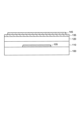
- FIG. 1 is a schematic cross-sectional view showing a configuration of a thin film transistor according to one embodiment of the present invention.
- 1 is a schematic plan view illustrating a configuration of a thin film transistor according to an embodiment of the present invention.
- FIG. 1 is a schematic diagram illustrating a TEM-ED mapping method.
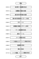
- 2 is a flowchart showing a method for manufacturing a thin film transistor according to an embodiment of the present invention.
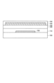
- 1A to 1C are schematic cross-sectional views showing a method for manufacturing a thin film transistor according to an embodiment of the present invention.
- 1A to 1C are schematic cross-sectional views showing a method for manufacturing a thin film transistor according to an embodiment of the present invention.
- 1A to 1C are schematic cross-sectional views showing a method for manufacturing a thin film transistor according to an embodiment of the present invention.
- 1A to 1C are schematic cross-sectional views showing a method for manufacturing a thin film transistor according to an embodiment of the present invention.
- 1A to 1C are schematic cross-sectional views showing a method for manufacturing a thin film transistor according to an embodiment of the present invention.
- 1A to 1C are schematic cross-sectional views showing a method for manufacturing a thin film transistor according to an embodiment of the present invention.
- 1A to 1C are schematic cross-sectional views showing a method for manufacturing a thin film transistor according to an embodiment of the present invention.
- 1A to 1C are schematic cross-sectional views showing a method for manufacturing a thin film transistor according to an embodiment of the present invention.
- 1 is a schematic diagram illustrating an electronic device according to an embodiment of the present invention.
- 11 is an inverse pole figure of an oxide semiconductor layer (Poly-OS film) of a sample according to an embodiment of the present invention.
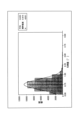
- 13 is an IPF map of an oxide semiconductor layer (Poly-OS film) of a sample according to an embodiment of the present invention. 1 shows a KAM map of an oxide semiconductor layer (Poly-OS film) of an example sample. 13 is a graph showing the distribution of KAM values of oxide semiconductor layers (Poly-OS films) of example samples. 13 is a graph showing the depth-average KAM value in oxide semiconductor layers (Poly-OS films) of example samples.
- the direction from the substrate toward the oxide semiconductor layer is referred to as “up” or “upper”. Conversely, the direction from the oxide semiconductor layer toward the substrate is referred to as “down” or “lower”.
- the terms “up” or “lower” are used in the explanation, but for example, the vertical relationship between the substrate and the oxide semiconductor layer may be arranged in a direction different from that shown in the figure.
- the expression “oxide semiconductor layer on a substrate” merely describes the vertical relationship between the substrate and the oxide semiconductor layer as described above, and other members may be arranged between the substrate and the oxide semiconductor layer.
- Up or “lower” refers to the order of stacking in a structure in which multiple layers are stacked, and when a pixel electrode is expressed above a thin film transistor, the thin film transistor and the pixel electrode may not overlap in a planar view. On the other hand, when a pixel electrode is expressed vertically above a thin film transistor, the thin film transistor and the pixel electrode overlap in a planar view.
- film and “layer” may be used interchangeably in some cases.
- the term “display device” refers to a structure that displays an image using an electro-optical layer.
- the term display device may refer to a display panel that includes an electro-optical layer, or a structure in which other optical components (e.g., polarizing components, backlights, touch panels, etc.) are attached to a display cell.
- the "electro-optical layer” may include a liquid crystal layer, an electroluminescent (EL) layer, an electrochromic (EC) layer, and an electrophoretic layer, unless a technical contradiction occurs.
- the thin film transistor 10 can be used in, for example, a display device, an integrated circuit (IC) such as a microprocessor (Micro-Processing Unit: MPU), or a memory circuit.
- IC integrated circuit
- MPU Micro-Processing Unit
- FIG. 1 is a schematic cross-sectional view showing the configuration of the thin film transistor 10 according to one embodiment of the present invention.
- Figure 2 is a schematic plan view showing the configuration of the thin film transistor according to one embodiment of the present invention.
- Figure 1 is a cross-sectional view taken along line AA' in Figure 2.
- the thin film transistor 10 includes a substrate 100, a light-shielding layer 105, a first insulating layer 110, a second insulating layer 120, a metal oxide layer 130, an oxide semiconductor layer 140, a gate insulating layer 150, a gate electrode 160, a third insulating layer 170, a fourth insulating layer 180, a source electrode 201, and a drain electrode 203.
- the light-shielding layer 105 is provided on the substrate 100.
- the first insulating layer 110 covers the upper surface and end surfaces of the light-shielding layer 105 and is provided on the substrate 100.
- the second insulating layer 120 is provided on the first insulating layer 110.
- the metal oxide layer 130 is provided on the second insulating layer 120.
- the oxide semiconductor layer 140 is provided on the metal oxide layer 130.
- the oxide semiconductor layer 140 is in contact with the metal oxide layer 130.
- the gate insulating layer 150 covers the upper surface and end surfaces of the oxide semiconductor layer 140 and the end surfaces of the metal oxide layer 130, and is provided on the second insulating layer 120.
- the gate electrode 160 overlaps the oxide semiconductor layer 140 and is provided on the gate insulating layer 150.
- the third insulating layer 170 covers the upper surface and end surfaces of the gate electrode 160 and is provided on the gate insulating layer 150.
- the fourth insulating layer 180 is provided on the third insulating layer 170.
- the gate insulating layer 150, the third insulating layer 170, and the fourth insulating layer 180 are provided with openings 171 and 173 through which a part of the upper surface of the oxide semiconductor layer 140 is exposed.
- the source electrode 201 is provided on the fourth insulating layer 180 and inside the opening 171, and is in contact with the oxide semiconductor layer 140.
- the drain electrode 203 is provided on the fourth insulating layer 180 and inside the opening 173, and is in contact with the oxide semiconductor layer 140.
- the source-drain electrode 200 when there is no particular distinction between the source electrode 201 and the drain electrode 203, they may be collectively referred to as the source-drain electrode 200.
- the oxide semiconductor layer 140 is divided into a source region S, a drain region D, and a channel region CH with respect to the gate electrode 160. That is, the oxide semiconductor layer 140 includes the channel region CH overlapping with the gate electrode 160, and the source region S and the drain region D not overlapping with the gate electrode 160. In the film thickness direction of the oxide semiconductor layer 140, the end of the channel region CH coincides with the end of the gate electrode 160.
- the channel region CH has semiconductor properties.
- Each of the source region S and the drain region D has conductor properties. Therefore, the electrical conductivity of the source region S and the drain region D is greater than the electrical conductivity of the channel region CH.
- the source electrode 201 and the drain electrode 203 are in contact with the source region S and the drain region D, respectively, and are electrically connected to the oxide semiconductor layer 140.
- the oxide semiconductor layer 140 may have a single-layer structure or a multilayer structure.
- each of the light-shielding layer 105 and the gate electrode 160 has a constant width in the D1 direction and extends in the D2 direction perpendicular to the D1 direction.
- the width of the light-shielding layer 105 is greater than the width of the gate electrode 160.
- the channel region CH completely overlaps with the light-shielding layer 105.
- the D1 direction corresponds to the direction in which a current flows from the source electrode 201 to the drain electrode 203 through the oxide semiconductor layer 140. Therefore, the length of the channel region CH in the D1 direction is the channel length L, and the width of the channel region CH in the D2 direction is the channel width W.
- the substrate 100 can support each layer constituting the thin film transistor 10.
- a rigid substrate having light transmission properties such as a glass substrate, a quartz substrate, or a sapphire substrate
- a rigid substrate having no light transmission properties such as a silicon substrate
- a flexible substrate having light transmission properties such as a polyimide resin substrate, an acrylic resin substrate, a siloxane resin substrate, or a fluororesin substrate, can also be used as the substrate.
- impurities may be introduced into the above-mentioned resin substrate.
- a substrate in which a silicon oxide film or a silicon nitride film is formed on the above-mentioned rigid substrate or flexible substrate can also be used as the substrate 100.
- the light-shielding layer 105 can reflect or absorb external light. As described above, the light-shielding layer 105 is provided with an area larger than the channel region CH of the oxide semiconductor layer 140, and therefore can block external light incident on the channel region CH. For example, aluminum (Al), copper (Cu), titanium (Ti), molybdenum (Mo), or tungsten (W), or an alloy or compound thereof, can be used as the light-shielding layer 105. In addition, if electrical conductivity is not required, the light-shielding layer 105 does not necessarily need to contain a metal. For example, a black matrix made of a black resin can be used as the light-shielding layer 105.
- the light-shielding layer 105 may have a single-layer structure or a laminated structure.
- the light-shielding layer 105 may have a laminated structure of a red color filter, a green color filter, and a blue color filter.
- the first insulating layer 110, the second insulating layer 120, the third insulating layer 170, and the fourth insulating layer 180 can prevent impurities from diffusing into the oxide semiconductor layer 140.
- the first insulating layer 110 and the second insulating layer 120 can prevent the diffusion of impurities contained in the substrate 100
- the third insulating layer 170 and the fourth insulating layer 180 can prevent the diffusion of impurities (e.g., water) entering from the outside.
- silicon oxynitride (SiO x N y ) and aluminum oxynitride (AlO x N y ) are silicon compounds and aluminum compounds, respectively, containing nitrogen (N) at a ratio (x>y) smaller than that of oxygen (O).
- Silicon oxynitride ( SiNxOy ) and aluminum oxynitride ( AlNxOy ) are silicon compounds and aluminum compounds that contain a smaller ratio of oxygen than nitrogen (x> y ).
- Each of the first insulating layer 110, the second insulating layer 120, the third insulating layer 170, and the fourth insulating layer 180 may have a single-layer structure or a multilayer structure.
- each of the first insulating layer 110, the second insulating layer 120, the third insulating layer 170, and the fourth insulating layer 180 may have a planarizing function, or may have a function of releasing oxygen by heat treatment.
- the second insulating layer 120 has a function of releasing oxygen by heat treatment, oxygen is released from the second insulating layer 120 by the heat treatment performed in the manufacturing process of the thin film transistor 10, and the released oxygen can be supplied to the oxide semiconductor layer 140.
- the gate electrode 160, the source electrode 201, and the drain electrode 203 are conductive.
- copper (Cu), aluminum (Al), titanium (Ti), chromium (Cr), cobalt (Co), nickel (Ni), molybdenum (Mo), hafnium (Hf), tantalum (Ta), tungsten (W), or bismuth (Bi), or an alloy or compound thereof can be used for each of the gate electrode 160, the source electrode 201, and the drain electrode 203.
- Each of the gate electrode 160, the source electrode 201, and the drain electrode 203 may have a single-layer structure or a multilayer structure.
- the gate insulating layer 150 includes an oxide having insulating properties. Specifically, silicon oxide (SiO x ), silicon oxynitride (SiO x N y ), aluminum oxide (AlO x ), aluminum oxynitride (AlO x N y ), or the like is used as the gate insulating layer 150.
- the gate insulating layer 150 preferably has a composition close to a stoichiometric ratio.
- the gate insulating layer 150 preferably has few defects.
- the gate insulating layer 150 may be made of an oxide in which no defects are observed when evaluated by electron spin resonance (ESR).
- the metal oxide layer 130 includes a metal oxide having insulating properties. Specifically, a metal oxide having a band gap of 4 eV or more and 10.0 eV or less is used as the metal oxide layer 130.
- a metal oxide containing one or more metal elements selected from aluminum (Al), magnesium (Mg), calcium (Ca), scandium (Sc), gallium (Ga), germanium (Ge), strontium (Sr), nickel (Ni), tantalum (Ta), yttrium (Y), zirconium (Zr), barium (Ba), hafnium (Hf), cobalt (Co), and lanthanoid elements is used.
- a metal oxide containing aluminum e.g., aluminum oxide, etc.
- a metal oxide containing aluminum has high barrier properties against gases such as oxygen or hydrogen.
- the metal oxide layer 130 can also function as a buffer layer for the oxide semiconductor layer 140. For example, by subjecting the oxide semiconductor layer 140 in contact with the metal oxide layer 130 to a heat treatment, the crystallinity of the oxide semiconductor layer 140 can be improved.
- the oxide semiconductor film contains indium (In) and at least one or more metal elements (M) other than indium.
- the composition ratio of the oxide semiconductor film is preferably such that the atomic ratio of indium and at least one or more metal elements satisfies formula (1). In other words, the ratio of indium to all metal elements in the oxide semiconductor film is preferably 50% or more.
- the crystal structure of the oxide semiconductor film preferably has a bixbyite structure. By increasing the ratio of indium, an oxide semiconductor film having a bixbyite structure can be formed.
- the metal element other than indium is not limited to one type of metal element.
- the metal element other than indium may include multiple types of metal elements.
- the oxide semiconductor film can be formed by sputtering.
- the composition of the oxide semiconductor film formed by sputtering depends on the composition of the sputtering target. With a sputtering target having the above-mentioned composition, an oxide semiconductor film without compositional deviation of metal elements can be formed by sputtering. Therefore, the composition of the metal elements (indium and other metal elements) of the oxide semiconductor film may be the same as the composition of the metal elements of the sputtering target.
- the composition of the metal elements of the oxide semiconductor film can be specified based on the composition of the metal elements of the sputtering target. Note that this is not limited to the above because the oxygen contained in the oxide semiconductor film changes depending on the process conditions of the sputtering.
- the composition of the metal elements in the oxide semiconductor film can also be determined using X-ray fluorescence analysis or Electron Probe Micro Analyzer (EPMA) analysis. Furthermore, since the oxide semiconductor film has a polycrystalline structure, the composition of the oxide semiconductor film can be determined using X-ray diffraction (XRD) method. Specifically, the composition of the metal elements in the oxide semiconductor film can be determined based on the crystal structure and lattice constant of the oxide semiconductor film obtained by XRD method.
- XRD X-ray diffraction
- the oxide semiconductor film has a polycrystalline structure including a plurality of crystal grains. Although details will be described later, by using a polycrystalline oxide semiconductor (Poly-OS) technique, an oxide semiconductor film having a novel polycrystalline structure different from a conventional one can be formed. Therefore, hereinafter, the oxide semiconductor film having a polycrystalline structure according to this embodiment may be referred to as a Poly-OS film in order to distinguish it from a conventional oxide semiconductor film having a polycrystalline structure.
- Poly-OS polycrystalline oxide semiconductor
- the crystal grains contained in the Poly-OS film may be composed of multiple crystallites.
- the crystallite diameter is not particularly limited, but is preferably 1 nm or more, more preferably 10 nm or more, and even more preferably 15 nm or more.
- the crystallite diameter can be obtained using an electron beam diffraction method, an XRD method, or the like.
- the crystal structure of the Poly-OS film is not particularly limited, but is preferably a bixbyite structure.
- the crystal structure of the Poly-OS film can be identified using the XRD method or the electron beam diffraction method.
- the multiple crystal grains may have one type of crystal structure, or may have multiple types of crystal structures.
- the Poly-OS film has multiple types of crystal structures, it is preferable that one of the multiple types of crystal structures is a bixbyite structure.
- the crystal structure of the Poly-OS film is different from that of a conventional oxide semiconductor film having a polycrystalline structure.
- the inventors have found that the crystal grains contained in the Poly-OS film have characteristics different from those of the crystal grains contained in a conventional oxide semiconductor film.
- Such characteristics of the Poly-OS film can be obtained by measuring the crystal orientation (perpendicular to the crystal plane) using an electron diffraction pattern.
- the characteristics of the Poly-OS film can be measured using a TEM-ED mapping (Transmission Electron Microscopy Electron Diffraction Mapping) method.
- the TEM-ED mapping method is sometimes called the ACOM-TEM (Automated Crystal Orientation Mapping Transmission Electron Microscopy) method. The following describes the measurement of an oxide semiconductor film using the TEM-ED mapping method.
- FIG. 3 is a schematic diagram for explaining the TEM-ED mapping method.
- the TEM-ED mapping method is an analysis method in which an electron beam is irradiated onto a measurement region of an object to be measured, an electron diffraction pattern observed after passing through the object to be measured is analyzed, and the crystal orientation in the measurement region of the object to be measured is measured. By continuously analyzing the electron diffraction pattern at a plurality of measurement points in the measurement region, information on the crystal orientation within or between crystal grains can be obtained.
- a TEM sample 500 is used as the object to be measured. Therefore, the TEM-ED mapping method can obtain information on the crystal orientation in a smaller measurement region than the EBSD (Electron Back Scattered Diffraction) method using a SEM sample.
- EBSD Electro Back Scattered Diffraction
- the TEM-ED mapping method is applied to the oxide semiconductor layer 140 of the thin-film transistor 10
- a thin-film sample including a cross section of the oxide semiconductor layer 140 of the thin-film transistor 10 is used as the TEM sample 500.
- the TEM-ED mapping method is a measurement of a microscopic region using a TEM sample, and the step interval of the measurement points at which the electron beam diffraction pattern is observed is, for example, 1 nm or more, but is not limited to this. However, in measuring the crystal orientation, it is preferable to have a large number of measurement points in the film thickness direction of the oxide semiconductor layer 140.
- the step interval is 1/5 or less of the film thickness of the oxide semiconductor layer, preferably 1/10 or less, and more preferably 1/30 or less.
- a coordinate system based on the TEM sample 500 (ND (Normal Direction), TD (Transverse Direction), and RD (Reference Direction)) is used.
- ND Normal Direction
- TD Transverse Direction
- RD Reference Direction
- the normal direction to the surface of the TEM sample 500 is ND.
- ND, TD, and RD are mutually orthogonal.
- the electron beam is irradiated from the ND to the TEM 500.
- a coordinate system (x-axis, y-axis, and z-axis) based on the thin-film transistor 10 (or the oxide semiconductor layer 140) is shown, along with a coordinate system based on the TEM sample 500.
- the film thickness direction of the oxide semiconductor layer 140 is the z-axis.
- the x-axis, y-axis, and z-axis are mutually orthogonal. Therefore, the x-axis and y-axis are in-plane directions of the oxide semiconductor layer 140.
- ND, TD, and RD in the TEM-ED mapping method correspond to the y-axis, x-axis, and z-axis of the thin-film transistor 10, respectively.
- An inverse pole figure is an image illustrating crystal orientations in a specific direction of a coordinate system based on the TEM sample 500.
- the proportion of crystal orientations in each direction of the coordinate system of the TEM sample 500 is shown according to a predetermined index.
- the proportion of crystal orientations in a specific direction is color-coded according to a color key.
- IPF Map An IPF map is an image in which crystal orientations in a specific direction of a coordinate system based on the TEM sample 500 are illustrated as a distribution of crystal orientations on the surface of the TEM sample 500.
- crystal orientations at multiple measurement points are classified according to a predetermined index indicating the crystal orientation in each direction of the coordinate system of the TEM sample 500.
- the crystal orientations are color-coded according to a color key.
- a crystal grain is a crystalline region surrounded by a crystal grain boundary. Since the TEM-ED mapping method can obtain information about the crystal orientation, the crystal grain boundary can be defined based on the crystal orientation. In general, when the difference in crystal orientation between two adjacent measurement points exceeds 5°, it is defined that a crystal grain boundary exists between the two measurement points. Therefore, the above definition is also applied to the Poly-OS film.
- the TEM-ED mapping method is a measurement in a minute measurement region.
- a thin film sample having a surface along a cross section in the film thickness direction is used as the TEM sample 500, it is difficult to define the grain size of the crystal grains spreading in the plane of the oxide semiconductor layer 140. Therefore, in this embodiment, instead of the grain size, the length of the crystal grain obtained based on the cross section of the oxide semiconductor layer 140 in the measurement region is defined as the grain length. Specifically, the distance between two grain boundaries obtained in the cross section of the oxide semiconductor layer 140 is defined as the grain length. The grain length defined in this way may be calculated to be smaller than the grain size.
- the grain size of the crystal grains contained in the Poly-OS film is significantly larger than the grain size of the crystal grains contained in a conventional oxide semiconductor film. That is, the grain length defined as above in the Poly-OS film can be obtained as a value larger than the grain size of the crystal grains contained in a conventional oxide semiconductor film. Therefore, it is possible to compare the Poly-OS film with the conventional oxide semiconductor film by using the grain length defined as above.
- the crystal grain length is 100 nm or more, preferably 300 nm or more, and more preferably 500 nm or more.
- the upper limit of the crystal grain length is not particularly limited, but is 50 ⁇ m or less.
- the crystal grain length is preferably measured at the center of the film thickness.
- the crystal grains contained in the Poly-OS film have a large crystal grain length, and one crystal grain may form part of the upper surface and part of the lower surface of the Poly-OS film.
- the crystal grain boundary between two adjacent crystal grains is formed from the upper surface to the lower surface (or from the lower surface to the upper surface), but is not formed along the film thickness direction, and the position of the upper surface and the position of the lower surface of the crystal grain boundary may be misaligned.
- two adjacent crystal grains sandwiching a crystal grain boundary overlap each other in the film thickness direction of the Poly-OS film.
- the distance between the position of the upper surface and the position of the lower surface of the crystal grain boundary in the direction perpendicular to the film thickness direction of the Poly-OS film is, for example, 10 nm or more, preferably 20 nm or more, and more preferably 30 nm or more.
- KAM Kernel Average Misorientation
- the KAM (Kernel Average Misorientation) value is the average value of the crystal orientation misorientation between one measurement point in a crystal grain and all measurement points adjacent to that measurement point. The crystal orientation misorientation between two adjacent measurement points across a grain boundary is excluded from the calculation of the KAM value.
- the KAM value is a value that represents the change in crystal orientation within a crystal grain. As mentioned above, if the difference in crystal orientation between one measurement point and another measurement point adjacent to that measurement point exceeds 5°, it is considered to be a grain boundary. Therefore, the range of KAM values calculated based on adjacent measurement points within a crystal grain is 0° or more and 5° or less. A large KAM value means that there is a large change in local crystal orientation within the crystal grain, and that the crystal grain is highly distorted.
- the KAM value is calculated at each of the multiple measurement points. Therefore, a distribution diagram of the KAM value within the crystal grain can be created. In addition, the average value and standard deviation of the KAM value can be calculated.
- the average value of the KAM value is a value that represents one of the properties of the crystal grains contained in the Poly-OS film. Since the Poly-OS film has a large change in crystal orientation and contains many crystals with large distortion, the average value of the KAM value is larger than that of a conventional oxide semiconductor film having a polycrystalline structure.
- the average value of the KAM value in the Poly-OS film is 0.6° or more, preferably 0.7° or more, and more preferably 0.8° or more.
- the standard deviation of the KAM value is also a value that represents one of the properties of the crystal grains contained in the Poly-OS film.
- the standard deviation of the KAM value is 0.3° or more, preferably 0.35° or more, and more preferably 0.4° or more.
- the average KAM value increases as the step spacing between the measurement points increases. This is due to the large change in crystal orientation within the crystal grains contained in the Poly-OS film, and the tendency for the average KAM value to increase as the step spacing increases is also one of the characteristics of the Poly-OS film.
- the average value of the KAM values described above is the total average value of the KAM values (KAM AVE(total)) calculated using the KAM values of all the measurement points in the measurement region. Unless otherwise specified in this specification, the average value of the KAM values refers to the total average value of the KAM values (KAM AVE(total) ) . On the other hand, it is also possible to calculate the average value of the KAM values using some of the measurement points in the measurement region. For example, the film thickness of the Poly-OS film can be divided, and the average value of the KAM values of the measurement points included in the divided regions can be calculated.
- the average value of the KAM values calculated using some of the measurement points is different from the total average value of the KAM values (KAM AVE(total) ).
- the average value of the KAM value calculated by dividing the thickness of the Poly-OS film depends on the distance (depth) of the thickness of the Poly-OS film. Therefore, in this specification, the average value is sometimes referred to as the depth average value of the KAM value (KAM AVE(depth) ) to be distinguished from the total average value of the KAM values (KAM AVE(total) ).
- the Poly-OS film may be formed of one crystal grain from the top surface to the bottom surface.
- the crystal orientation also changes significantly in the thickness direction of the Poly-OS film.
- the depth average value (KAM AVE(depth) ) of the KAM value is different between the top end and bottom end (near the interface, for example, within 3 nm from the interface) and the center (near the center, for example, within 5 nm equidistant from the top end and bottom end) of the Poly-OS film.
- the depth average value (KAM AVE(depth) ) of the KAM value at each of the top end and bottom end of the Poly-OS film is 0.6° or more and less than 5.0°, and preferably 0.7° or more and less than 5.0°.
- the depth average value of the KAM value (KAM AVE(depth) ) at the center of the Poly-OS film is less than 0.6°.
- the difference in the depth average value of the KAM value (KAM AVE(depth) ) between the upper or lower end and the center of the Poly-OS film is 0.1° or more, preferably 0.15° or more, and further preferably 0.2° or more.
- the upper and lower surfaces of the Poly-OS film may have unevenness.
- the number of measurement points at the upper and lower ends is reduced, and the error in the depth average value of the KAM values (KAM AVE(depth)) at the upper and lower ends is likely to be large. Therefore, the depth average value of the KAM values (KAM AVE(depth) ) at the upper and lower ends may be calculated by considering a region in which the number of measurement points included in the divided region is 90% or more of the number of measurement points in the center (or a region in which the number of measurement points is 90% or more of the maximum number of measurement points ) as a valid region.
- the depth average value of the KAM values (KAM AVE(depth) ) at the upper and lower ends can be calculated without being affected by the unevenness formed on the upper and lower surfaces.
- the TEM-ED mapping method can obtain information about the crystal orientation within the crystal grains contained in the Poly-OS film. For example, when the Poly-OS film has a bixbyite structure, the TEM-ED mapping method can be observed to show that the Poly-OS film contains crystal grains with a crystal orientation of ⁇ 001>, ⁇ 101>, or ⁇ 111>.
- the crystal orientation ⁇ 001> represents [001] and its equivalents [100] and [010].
- the crystal orientation ⁇ 101> represents [101] and its equivalents [110] and [011].
- the crystal orientation ⁇ 111> represents [111].
- "1" may be "-1", and is considered to be an axis equivalent to each orientation.
- crystal orientations such as ⁇ hk0> (h ⁇ k, h and k are natural numbers), ⁇ hhl> (h ⁇ l, h and l are natural numbers), and ⁇ hkl> (h ⁇ k ⁇ l, h, k, and l are natural numbers).
- the crystal grains contained in the Poly-OS film have a characteristic that the crystal orientation changes greatly within the crystal grain.
- the average KAM value of the Poly-OS film is 0.6° or more.
- the crystal grain size of the crystal grain becomes small.
- the crystal grain length (or crystal grain size) of the crystal grain is large.
- the Poly-OS film is less susceptible to the influence of crystal grain boundaries because it contains crystal grains with a large crystal grain length (or crystal grain size). Therefore, in the thin-film transistor 10 that includes a Poly-OS film as the channel, the channel is less susceptible to the influence of crystal grain boundaries, grain boundary scattering is suppressed, and the field-effect mobility is improved.
- the configuration of the thin film transistor 10 has been described above, but the above-mentioned thin film transistor 10 is a so-called top-gate type transistor.
- the thin film transistor 10 can be modified in various ways.
- the thin film transistor 10 may be configured such that the light-shielding layer 105 functions as a gate electrode, and the first insulating layer 110 and the second insulating layer 120 function as gate insulating layers.
- the thin film transistor 10 is a so-called dual-gate type transistor.
- the light-shielding layer 105 when the light-shielding layer 105 is conductive, the light-shielding layer 105 may be a floating electrode or may be connected to the source electrode 201.
- the thin film transistor 10 may be a so-called bottom-gate type transistor in which the light-shielding layer 105 functions as a main gate electrode.
- FIG. 4 is a flowchart showing a method for manufacturing the thin film transistor 10 according to one embodiment of the present invention.
- Fig. 5 to Fig. 12 are schematic cross-sectional views showing a method for manufacturing the thin film transistor 10 according to one embodiment of the present invention.
- the method for manufacturing the thin-film transistor 10 includes steps S1010 to S1110. Below, steps S1010 to S1110 will be described in order, but the order of the steps may be reversed in the method for manufacturing the thin-film transistor 10. In addition, the method for manufacturing the thin-film transistor 10 may include additional steps.
- a light-shielding layer 105 having a predetermined pattern is formed on the substrate 100.
- the light-shielding layer 105 is patterned using a photolithography method.
- a first insulating layer 110 and a second insulating layer 120 are formed on the light-shielding layer 105 (see FIG. 5).
- the first insulating layer 110 and the second insulating layer 120 are formed using a CVD method.
- silicon nitride and silicon oxide are formed as the first insulating layer 110 and the second insulating layer 120, respectively.
- silicon nitride is used as the first insulating layer 110
- the first insulating layer 110 can block impurities that are diffused from the substrate 100 side to the oxide semiconductor layer 140.
- silicon oxide is used as the second insulating layer 120, the second insulating layer 120 can release oxygen by heat treatment.
- a metal oxide film 135 is formed on the second insulating layer 120 (see FIG. 6).
- the metal oxide film 135 is formed by a sputtering method.
- the thickness of the metal oxide film 135 is, for example, 2 nm to 51 nm, preferably 2 nm to 31 nm, more preferably 2 nm to 21 nm, and particularly preferably 2 nm to 11 nm.
- an oxide semiconductor film 145 is formed on the metal oxide film 135 (see FIG. 6).
- the oxide semiconductor film 145 is formed by a sputtering method.
- the thickness of the oxide semiconductor film 145 is, for example, 10 nm or more and 100 nm or less, preferably 15 nm or more and 70 nm or less, and more preferably 15 nm or more and 40 nm or less.
- the oxide semiconductor film 145 in step S1020 is amorphous.
- the oxide semiconductor film 145 after film formation and before heat treatment is amorphous. Therefore, it is preferable that the film formation conditions of the oxide semiconductor film 145 are such that the oxide semiconductor film 145 immediately after film formation is not crystallized as much as possible.
- the oxide semiconductor film 145 is formed by a sputtering method, the oxide semiconductor film 145 is formed while controlling the temperature of the film formation target (the substrate 100 and the layer formed on the substrate 100) to 100° C. or less, preferably 80° C. or less, and more preferably 50° C. or less.
- the oxide semiconductor film 145 is formed under a condition of low oxygen partial pressure.
- the oxygen partial pressure is 2% or more and 20% or less, preferably 3% or more and 15% or less, and more preferably 3% or more and less than 10%.
- the oxide semiconductor film 145 is patterned (see FIG. 7).
- the oxide semiconductor film 145 is patterned using a photolithography method.
- the oxide semiconductor film 145 may be etched by wet etching or dry etching.
- an acidic etchant may be used.
- oxalic acid, PAN, sulfuric acid, hydrogen peroxide, or hydrofluoric acid may be used as the etchant.
- step S1040 a heat treatment is performed on the oxide semiconductor film 145.
- the heat treatment performed in step S1040 is referred to as "OS annealing".
- OS annealing the oxide semiconductor film 145 is held at a predetermined temperature for a predetermined time.
- the predetermined temperature is 300° C. or higher and 500° C. or lower, and preferably 350° C. or higher and 450° C. or lower.
- the predetermined time (holding time) at the temperature is 15 minutes or higher and 120 minutes or lower, and preferably 30 minutes or higher and 60 minutes or lower.
- the OS annealing crystallizes the oxide semiconductor film 145, and an oxide semiconductor layer 140 having a polycrystalline structure (i.e., an oxide semiconductor layer 140 including a Poly-OS film) is formed.
- the metal oxide film 135 is patterned to form the metal oxide layer 130 (FIG. 8).
- the metal oxide film 135 is etched using the oxide semiconductor layer 140 as a mask.
- the photolithography process can be omitted.
- the metal oxide film 135 may be etched by wet etching or dry etching. For example, diluted hydrofluoric acid (DHF) is used in wet etching.
- DHF diluted hydrofluoric acid
- the gate insulating layer 150 is formed on the oxide semiconductor layer 140 (see FIG. 9).
- the gate insulating layer 150 is formed using a CVD method.
- silicon oxide is formed as the gate insulating layer 150.
- the gate insulating layer 150 may be formed at a film formation temperature of 350° C. or higher.
- the thickness of the gate insulating layer 150 is 50 nm or more and 300 nm or less, preferably 60 nm or more and 200 nm or less, and more preferably 70 nm or more and 150 nm or less.
- step S1060 a heat treatment is performed on the oxide semiconductor layer 140.
- the heat treatment performed in step S1060 is referred to as "oxidation annealing.”
- oxidation annealing When the gate insulating layer 150 is formed on the oxide semiconductor layer 140, many oxygen defects are generated on the upper and side surfaces of the oxide semiconductor layer 140.
- oxygen is supplied from the second insulating layer 120 and the gate insulating layer 150 to the oxide semiconductor layer 140, and the oxygen defects are repaired.
- a gate electrode 160 having a predetermined pattern is formed on the gate insulating layer 150 (see FIG. 10).
- the gate electrode 160 is formed by sputtering or atomic layer deposition, and the gate electrode 160 is patterned using photolithography.
- a source region S and a drain region D are formed in the oxide semiconductor layer 140 (see FIG. 10).
- the source region S and the drain region D are formed by ion implantation.
- impurities are implanted into the oxide semiconductor layer 140 through the gate insulating layer 150 using the gate electrode 160 as a mask.
- argon (Ar), phosphorus (P), or boron (B) is used as the implanted impurity.
- oxygen vacancies are generated by the ion implantation, and hydrogen is trapped in the generated oxygen vacancies. This reduces the resistance of the source region S and the drain region D.
- impurities are not implanted, so no oxygen vacancies are generated and the resistance of the channel region CH does not decrease.
- the gate insulating layer 150 may also contain impurities such as argon (Ar), phosphorus (P), or boron (B).
- a third insulating layer 170 and a fourth insulating layer 180 are formed on the gate insulating layer 150 and the gate electrode 160 (see FIG. 11).
- the third insulating layer 170 and the fourth insulating layer 180 are formed using a CVD method.
- silicon oxide and silicon nitride are formed as the third insulating layer 170 and the fourth insulating layer 180, respectively.
- the thickness of the third insulating layer 170 is 50 nm or more and 500 nm or less.
- the thickness of the fourth insulating layer 180 is also 50 nm or more and 500 nm or less.
- openings 171 and 173 are formed in the gate insulating layer 150, the third insulating layer 170, and the fourth insulating layer 180 (see FIG. 12). By forming the openings 171 and 173, the source region S and the drain region D of the oxide semiconductor layer 140 are exposed.
- a source electrode 201 is formed on the fourth insulating layer 180 and inside the opening 171
- a drain electrode 203 is formed on the fourth insulating layer 180 and inside the opening 173.
- the source electrode 201 and the drain electrode 203 are formed as the same layer. Specifically, the source electrode 201 and the drain electrode 203 are formed by patterning a single conductive film that has been deposited. Through these steps, the thin-film transistor 10 shown in FIG. 1 is manufactured.
- the oxide semiconductor layer 140 includes a Poly-OS film having a novel crystal structure.
- the Poly-OS film has a large change in crystal orientation and includes crystal grains with a large crystal grain length (or crystal grain size). Therefore, in the thin film transistor 10 including the Poly-OS film as the channel, the channel as a whole is less susceptible to the influence of the crystal grain boundaries. It is also considered that the crystal orientation within the crystal grains changes so as to improve the lattice matching at the crystal grain boundaries, and as a result, crystal grain boundaries with fewer defects are generated. For these reasons, in the thin film transistor 10 including the Poly-OS film as the channel, grain boundary scattering is suppressed and the field effect mobility is improved.
- FIG. 13 is a schematic diagram showing an electronic device 1000 according to one embodiment of the present invention.
- FIG. 13 shows a smartphone, which is an example of the electronic device 1000.
- the electronic device 1000 includes a display device 1100 with curved sides.
- the display device 1100 includes a plurality of pixels for displaying an image, and the plurality of pixels are controlled by a pixel circuit, a drive circuit, and the like.
- the pixel circuit and drive circuit include the thin-film transistor 10 described in the first embodiment.
- the thin-film transistor 10 has high field-effect mobility, and therefore improves the responsiveness of the pixel circuit and the drive circuit, and as a result, the performance of the electronic device 1000 can be improved.
- the electronic device 1000 is not limited to a smartphone.
- the electronic device 1000 also includes electronic devices having a display device, such as a watch, a tablet, a notebook computer, a car navigation system, or a television.
- the thin-film transistor 10 described in the first embodiment can be applied to any electronic device, regardless of whether or not it has a display device.
- oxide semiconductor layer specifically, the Poly-OS film
- a thin film transistor was fabricated using the manufacturing method described in the first embodiment.
- a sputtering target in which indium is 70% in atomic ratio to all metal elements contained in the sintered body was used to form an oxide semiconductor layer with a thickness of 30 nm.
- the oxygen partial pressure during film formation was 5%, and the substrate temperature was controlled to be 100° C. or less.
- the OS annealing process the ultimate temperature was controlled between 350° C. and 450° C. in an air atmosphere, and the ultimate temperature was held for 60 minutes.
- the chemical composition of the oxide semiconductor layer after the OS annealing process was the same as that of the sputtering target.
- Example sample A TEM sample (hereinafter referred to as an "example sample”) was prepared by sampling a cross section of a region including an oxide semiconductor layer of a thin film transistor by FIB processing, and a crystal orientation analysis of a Poly-OS film included in the oxide semiconductor layer was performed by TEM-ED mapping.
- the measurement conditions for the TEM-ED mapping are shown in Table 1.
- An ASTAR manufactured by NanoMegas Corp. was used for the analysis of the crystal orientation.
- PDF powder diffraction file
- FIG. 14 is an inverse pole figure of the oxide semiconductor layer (Poly-OS film) of the example sample.
- FIG. 14 shows inverse pole figures for ND, TD, and RD.
- the proportion of the crystal orientation increases according to the value of the index shown in FIG. 14 (for example, the index may be a color key, and the proportion of the crystal orientation increases as the color changes from blue to red (the wavelength of visible light increases)).
- the index may be a color key
- the proportion of the crystal orientation increases as the color changes from blue to red (the wavelength of visible light increases)
- regions A1, A2, and A3 there are regions having large values, and it was found that there are specific crystal orientations with a large proportion.
- the proportion of the crystal orientation ⁇ 111> is larger than that of the crystal orientation ⁇ 001> and the crystal orientation ⁇ 101>.
- IPF map 15 is an IPF map of an oxide semiconductor layer (Poly-OS film) of an example sample. IPF maps for ND, TD, and RD are shown in Fig. 15. In Fig. 15, the crystal orientation ⁇ 001>, the crystal orientation ⁇ 101>, the crystal orientation ⁇ 111>, and the crystal orientation ⁇ 011> are classified according to the indexes in the figure.
- the crystal orientation changed significantly and discontinuously.
- the discontinuous change in crystal orientation corresponds to a grain boundary, and in regions B1 and B2, a grain boundary was confirmed to have formed from the top surface to the bottom surface (or from the bottom surface to the top surface) of the oxide semiconductor layer.
- the grain length of one crystal grain between the grain boundary in region B1 and the grain boundary in region B2 was 1080 nm.
- one crystal grain formed part of the top surface and part of the bottom surface of the oxide semiconductor layer. In other words, the grain length was 10 times or more the thickness of the oxide semiconductor layer.
- the crystal orientations within the grains in the IPF map corresponded to the proportion of crystal orientations in the inverse pole figures described above.
- the main crystal orientation of the grains in the RD is the crystal orientation ⁇ 111>.
- the grain boundary in region B2 was not formed along the film thickness direction of the oxide semiconductor layer, but was significantly shifted from the film thickness direction of the oxide semiconductor layer. In other words, two adjacent crystal grains sandwiching the grain boundary in region B2 overlapped each other in the film thickness direction of the oxide semiconductor layer. In the direction perpendicular to the film thickness direction of the oxide semiconductor layer, the overlap distance of two adjacent crystal grains was 34 nm.
- KAM value 16 is a KAM map of the oxide semiconductor layer (Poly-OS film) of the example sample. Specifically, in FIG. 16, the KAM values of the measurement points in the measurement region are classified according to the values of the indices shown in FIG. 16 (for example, the indices may be a color key, and the KAM value increases from 0° to 5° as the color changes from blue to red (the wavelength of visible light increases)). Note that when the crystal orientation difference between two adjacent measurement points exceeds 5°, it is regarded as a grain boundary, and therefore the upper limit of the KAM value is 5°.
- FIG. 17 is a graph showing the distribution of the KAM values of the oxide semiconductor layer (Poly-OS film) of the example sample.
- the oxide semiconductor layer has not only a region having a KAM value near 0° (corresponding to the region shown in blue in the color key, hereinafter, for convenience of explanation, it will be referred to as the "blue region"), but also a region having a KAM value other than near 0° (corresponding to the region shown in green in the color key, hereinafter, for convenience of explanation, it will be referred to as the "green region”).
- the blue region spread in the center of the oxide semiconductor layer, and the green region spread near the surface (near the upper end and the lower end) of the oxide semiconductor layer.
- the TEM-ED mapping method is a measurement in a microscopic area, but in the case of the Poly-OS film, the total average value and standard deviation of the KAM value are large even in such a microscopic area. This means that there is a large change in the crystal orientation within the crystal grains of the Poly-OS film. Although the crystal grains contained in the Poly-OS film have a large crystal grain length (or crystal grain size), there is a large change in the local crystal orientation. This is one of the characteristics of the Poly-OS film that is not seen in conventional oxide semiconductor films having a polycrystalline structure.
- FIG. 18 is a graph showing the depth average value of the KAM value in the oxide semiconductor layer (Poly-OS film) of the example sample.
- the KAM values of the measurement points were collected for each distance from the interface between the gate insulating layer and the oxide semiconductor layer (depth of the oxide semiconductor layer), and the depth average value of the KAM value (KAM AVE(depth) ) was calculated, which is the average value.
- the depth average value of the KAM value (KAM AVE(depth) ) is the average value of the KAM values of some measurement points divided according to the depth of the oxide semiconductor layer.
- a region in which the number of measurement points included in the divided region is 90% or more of the number of measurement points in the center part was set as a valid region, and the depth average value of the KAM value (KAM AVE(depth) ) of the oxide semiconductor layer was calculated.
- the depth average value of the KAM value (KAM AVE(depth) ) is plotted against the thickness direction of the oxide semiconductor layer.
- the average depth value of the KAM value (KAM AVE(depth)) was larger at the upper end portion near the interface between the oxide semiconductor layer and the gate insulating layer and at the lower end portion near the interface between the oxide semiconductor layer and the metal oxide layer than at the central portion of the oxide semiconductor layer.
- the average depth values of the KAM value (KAM AVE(depth) ) at the central portion (depth 15 nm), upper end portion (depth 0 nm), and lower end portion (depth 32 nm) were 0.554°, 0.828°, and 0.802°, respectively.
- the difference in the average depth value of the KAM value (KAM AVE(depth) ) between the upper end portion and the central portion, and the difference between the lower end portion and the central portion were 0.2° or more.
- the above results indicate that there is a large change in crystal orientation near the interface of the oxide semiconductor layer.
- the local change in crystal orientation is also large in the film thickness direction.
- the crystal grain length (or crystal grain size) is small so that the distortion in the crystal grains is relieved, and it is difficult to form the oxide semiconductor film from the top to the bottom with a single crystal grain.
- the Poly-OS film it is possible to form the oxide semiconductor film from the top to the bottom with a single crystal grain that has a large change in crystal orientation. This is one of the characteristics of the Poly-OS film that is not seen in a conventional oxide semiconductor film having a polycrystalline structure.
Landscapes
- Thin Film Transistor (AREA)
Priority Applications (5)
| Application Number | Priority Date | Filing Date | Title |
|---|---|---|---|
| KR1020257022126A KR20250117810A (ko) | 2023-03-17 | 2024-03-12 | 박막 트랜지스터 및 전자 기기 |
| CN202480006547.4A CN120570087A (zh) | 2023-03-17 | 2024-03-12 | 薄膜晶体管及电子设备 |
| JP2025508339A JPWO2024195629A1 (https=) | 2023-03-17 | 2024-03-12 | |
| DE112024000552.7T DE112024000552T5 (de) | 2023-03-17 | 2024-03-12 | Dünnschichttransistor und elektronische vorrichtung |
| US19/319,774 US20260006849A1 (en) | 2023-03-17 | 2025-09-05 | Thin film transistor and electronic device |
Applications Claiming Priority (2)
| Application Number | Priority Date | Filing Date | Title |
|---|---|---|---|
| JP2023-043065 | 2023-03-17 | ||
| JP2023043065 | 2023-03-17 |
Related Child Applications (1)
| Application Number | Title | Priority Date | Filing Date |
|---|---|---|---|
| US19/319,774 Continuation US20260006849A1 (en) | 2023-03-17 | 2025-09-05 | Thin film transistor and electronic device |
Publications (1)
| Publication Number | Publication Date |
|---|---|
| WO2024195629A1 true WO2024195629A1 (ja) | 2024-09-26 |
Family
ID=92842100
Family Applications (1)
| Application Number | Title | Priority Date | Filing Date |
|---|---|---|---|
| PCT/JP2024/009575 Ceased WO2024195629A1 (ja) | 2023-03-17 | 2024-03-12 | 薄膜トランジスタおよび電子機器 |
Country Status (7)
| Country | Link |
|---|---|
| US (1) | US20260006849A1 (https=) |
| JP (1) | JPWO2024195629A1 (https=) |
| KR (1) | KR20250117810A (https=) |
| CN (1) | CN120570087A (https=) |
| DE (1) | DE112024000552T5 (https=) |
| TW (1) | TWI899892B (https=) |
| WO (1) | WO2024195629A1 (https=) |
Citations (3)
| Publication number | Priority date | Publication date | Assignee | Title |
|---|---|---|---|---|
| JP2012253315A (ja) * | 2010-12-28 | 2012-12-20 | Idemitsu Kosan Co Ltd | 酸化物半導体薄膜層を有する積層構造及び薄膜トランジスタ |
| JP2015173259A (ja) * | 2014-02-19 | 2015-10-01 | 株式会社半導体エネルギー研究所 | 酸化物、半導体装置、モジュールおよび電子機器 |
| JP2016180178A (ja) * | 2015-03-13 | 2016-10-13 | 株式会社半導体エネルギー研究所 | 酸化物およびその作製方法 |
Family Cites Families (9)
| Publication number | Priority date | Publication date | Assignee | Title |
|---|---|---|---|---|
| JP2003273016A (ja) * | 2002-01-11 | 2003-09-26 | Sharp Corp | 半導体膜およびその形成方法、並びに、その半導体膜を用いた半導体装置、ディスプレイ装置。 |
| US8871565B2 (en) | 2010-09-13 | 2014-10-28 | Semiconductor Energy Laboratory Co., Ltd. | Method for manufacturing semiconductor device |
| EP2880690B1 (en) | 2012-08-03 | 2019-02-27 | Semiconductor Energy Laboratory Co. Ltd. | Semiconductor device with oxide semiconductor stacked film |
| TWI761605B (zh) | 2012-09-14 | 2022-04-21 | 日商半導體能源研究所股份有限公司 | 半導體裝置及其製造方法 |
| KR102220279B1 (ko) | 2012-10-19 | 2021-02-24 | 가부시키가이샤 한도오따이 에네루기 켄큐쇼 | 산화물 반도체막을 포함하는 다층막 및 반도체 장치의 제작 방법 |
| US9425217B2 (en) | 2013-09-23 | 2016-08-23 | Semiconductor Energy Laboratory Co., Ltd. | Semiconductor device |
| US9368582B2 (en) * | 2013-11-04 | 2016-06-14 | Avogy, Inc. | High power gallium nitride electronics using miscut substrates |
| CN109121438B (zh) | 2016-02-12 | 2022-02-18 | 株式会社半导体能源研究所 | 半导体装置以及包括该半导体装置的显示装置 |
| WO2022202795A1 (ja) * | 2021-03-26 | 2022-09-29 | 三菱マテリアル株式会社 | 金属板材、積層体、および、絶縁回路基板 |
-
2024
- 2024-03-12 WO PCT/JP2024/009575 patent/WO2024195629A1/ja not_active Ceased
- 2024-03-12 CN CN202480006547.4A patent/CN120570087A/zh active Pending
- 2024-03-12 JP JP2025508339A patent/JPWO2024195629A1/ja active Pending
- 2024-03-12 DE DE112024000552.7T patent/DE112024000552T5/de active Pending
- 2024-03-12 KR KR1020257022126A patent/KR20250117810A/ko active Pending
- 2024-03-15 TW TW113109602A patent/TWI899892B/zh active
-
2025
- 2025-09-05 US US19/319,774 patent/US20260006849A1/en active Pending
Patent Citations (3)
| Publication number | Priority date | Publication date | Assignee | Title |
|---|---|---|---|---|
| JP2012253315A (ja) * | 2010-12-28 | 2012-12-20 | Idemitsu Kosan Co Ltd | 酸化物半導体薄膜層を有する積層構造及び薄膜トランジスタ |
| JP2015173259A (ja) * | 2014-02-19 | 2015-10-01 | 株式会社半導体エネルギー研究所 | 酸化物、半導体装置、モジュールおよび電子機器 |
| JP2016180178A (ja) * | 2015-03-13 | 2016-10-13 | 株式会社半導体エネルギー研究所 | 酸化物およびその作製方法 |
Also Published As
| Publication number | Publication date |
|---|---|
| KR20250117810A (ko) | 2025-08-05 |
| CN120570087A (zh) | 2025-08-29 |
| TW202439617A (zh) | 2024-10-01 |
| US20260006849A1 (en) | 2026-01-01 |
| TWI899892B (zh) | 2025-10-01 |
| DE112024000552T5 (de) | 2025-12-11 |
| JPWO2024195629A1 (https=) | 2024-09-26 |
Similar Documents
| Publication | Publication Date | Title |
|---|---|---|
| US20250176237A1 (en) | Oxide semiconductor film, thin film transistor, and electronic device | |
| US20250176219A1 (en) | Thin film transistor and electronic device | |
| WO2024195629A1 (ja) | 薄膜トランジスタおよび電子機器 | |
| US20250393248A1 (en) | Thin film transistor and electronic device | |
| WO2025069956A1 (ja) | 薄膜トランジスタおよび電子機器 | |
| WO2025069957A1 (ja) | 酸化物半導体膜、薄膜トランジスタ、および電子機器 | |
| TWI914630B (zh) | 氧化物半導體膜、薄膜電晶體及電子機器 | |
| TWI899894B (zh) | 氧化物半導體膜、積層結構體、薄膜電晶體、及電子機器 | |
| US20260006848A1 (en) | Oxide semiconductor film, thin film transistor, and electronic device | |
| US20250176222A1 (en) | Oxide semiconductor film, thin film transistor, and electronic device | |
| KR102944325B1 (ko) | 박막 트랜지스터 및 전자 기기 | |
| US20250331259A1 (en) | Laminated structure, thin film transistor, and electronic device | |
| TW202610461A (zh) | 薄膜電晶體及電子機器 |
Legal Events
| Date | Code | Title | Description |
|---|---|---|---|
| 121 | Ep: the epo has been informed by wipo that ep was designated in this application |
Ref document number: 24774768 Country of ref document: EP Kind code of ref document: A1 |
|
| WWE | Wipo information: entry into national phase |
Ref document number: 1020257022126 Country of ref document: KR Ref document number: 202480006547.4 Country of ref document: CN |
|
| ENP | Entry into the national phase |
Ref document number: 2025508339 Country of ref document: JP Kind code of ref document: A |
|
| WWE | Wipo information: entry into national phase |
Ref document number: 2025508339 Country of ref document: JP |
|
| WWP | Wipo information: published in national office |
Ref document number: 1020257022126 Country of ref document: KR |
|
| WWP | Wipo information: published in national office |
Ref document number: 202480006547.4 Country of ref document: CN |
|
| WWE | Wipo information: entry into national phase |
Ref document number: 112024000552 Country of ref document: DE |
|
| WWP | Wipo information: published in national office |
Ref document number: 112024000552 Country of ref document: DE |
|
| 122 | Ep: pct application non-entry in european phase |
Ref document number: 24774768 Country of ref document: EP Kind code of ref document: A1 |