WO2024190452A1 - 半導体リレー及びこれを備えた電気部品ユニット - Google Patents
半導体リレー及びこれを備えた電気部品ユニット Download PDFInfo
- Publication number
- WO2024190452A1 WO2024190452A1 PCT/JP2024/007704 JP2024007704W WO2024190452A1 WO 2024190452 A1 WO2024190452 A1 WO 2024190452A1 JP 2024007704 W JP2024007704 W JP 2024007704W WO 2024190452 A1 WO2024190452 A1 WO 2024190452A1
- Authority
- WO
- WIPO (PCT)
- Prior art keywords
- light
- mosfet
- semiconductor relay
- source electrode
- connection conductor
- Prior art date
- Legal status (The legal status is an assumption and is not a legal conclusion. Google has not performed a legal analysis and makes no representation as to the accuracy of the status listed.)
- Ceased
Links
Images












Classifications
-
- H—ELECTRICITY
- H10—SEMICONDUCTOR DEVICES; ELECTRIC SOLID-STATE DEVICES NOT OTHERWISE PROVIDED FOR
- H10F—INORGANIC SEMICONDUCTOR DEVICES SENSITIVE TO INFRARED RADIATION, LIGHT, ELECTROMAGNETIC RADIATION OF SHORTER WAVELENGTH OR CORPUSCULAR RADIATION
- H10F55/00—Radiation-sensitive semiconductor devices covered by groups H10F10/00, H10F19/00 or H10F30/00 being structurally associated with electric light sources and electrically or optically coupled thereto
- H10F55/10—Radiation-sensitive semiconductor devices covered by groups H10F10/00, H10F19/00 or H10F30/00 being structurally associated with electric light sources and electrically or optically coupled thereto wherein the radiation-sensitive semiconductor devices control the electric light source, e.g. image converters, image amplifiers or image storage devices
- H10F55/15—Radiation-sensitive semiconductor devices covered by groups H10F10/00, H10F19/00 or H10F30/00 being structurally associated with electric light sources and electrically or optically coupled thereto wherein the radiation-sensitive semiconductor devices control the electric light source, e.g. image converters, image amplifiers or image storage devices wherein the radiation-sensitive devices and the electric light source are all semiconductor devices
-
- H—ELECTRICITY
- H03—ELECTRONIC CIRCUITRY
- H03K—PULSE TECHNIQUE
- H03K17/00—Electronic switching or gating, i.e. not by contact-making and –breaking
- H03K17/51—Electronic switching or gating, i.e. not by contact-making and –breaking characterised by the components used
- H03K17/78—Electronic switching or gating, i.e. not by contact-making and –breaking characterised by the components used using opto-electronic devices, i.e. light-emitting and photoelectric devices electrically- or optically-coupled
-
- H—ELECTRICITY
- H03—ELECTRONIC CIRCUITRY
- H03K—PULSE TECHNIQUE
- H03K17/00—Electronic switching or gating, i.e. not by contact-making and –breaking
- H03K17/51—Electronic switching or gating, i.e. not by contact-making and –breaking characterised by the components used
- H03K17/78—Electronic switching or gating, i.e. not by contact-making and –breaking characterised by the components used using opto-electronic devices, i.e. light-emitting and photoelectric devices electrically- or optically-coupled
- H03K17/785—Electronic switching or gating, i.e. not by contact-making and –breaking characterised by the components used using opto-electronic devices, i.e. light-emitting and photoelectric devices electrically- or optically-coupled controlling field-effect transistor switches
-
- H—ELECTRICITY
- H10—SEMICONDUCTOR DEVICES; ELECTRIC SOLID-STATE DEVICES NOT OTHERWISE PROVIDED FOR
- H10F—INORGANIC SEMICONDUCTOR DEVICES SENSITIVE TO INFRARED RADIATION, LIGHT, ELECTROMAGNETIC RADIATION OF SHORTER WAVELENGTH OR CORPUSCULAR RADIATION
- H10F77/00—Constructional details of devices covered by this subclass
- H10F77/93—Interconnections
-
- H—ELECTRICITY
- H10—SEMICONDUCTOR DEVICES; ELECTRIC SOLID-STATE DEVICES NOT OTHERWISE PROVIDED FOR
- H10W—GENERIC PACKAGES, INTERCONNECTIONS, CONNECTORS OR OTHER CONSTRUCTIONAL DETAILS OF DEVICES COVERED BY CLASS H10
- H10W90/00—Package configurations
Definitions
- This disclosure relates to a semiconductor relay and an electrical component unit equipped with the same.
- Patent Document 1 the configuration shown in Patent Document 1 has been proposed.
- a light-emitting element mounted on the input terminal and a light-receiving element mounted on the output terminal are arranged facing each other inside the housing. Both the input terminal and the output terminal are bent once along the middle, and their tip portions protrude outside the housing along the bottom surface of the housing.
- this semiconductor relay When this semiconductor relay is mounted on a circuit board on whose upper surface a signal line and a ground line are formed, the distance between the light receiving element and the element mounting portion of the input terminal on which the light receiving element is mounted can be increased, and the ground line or the ground plane formed on the lower surface of the circuit board.
- the ground line and ground plane are both electrically connected to the ground potential. This makes it possible to reduce the capacitance value of the parasitic capacitance generated between each mounting portion of the semiconductor relay and the ground potential, and thus reduces insertion loss.
- the semiconductor relay includes a first input terminal, a second input terminal, a light-emitting element electrically connected to the first input terminal and the second input terminal, a light-receiving driving element having a light-receiving element for receiving light output from the light-emitting element and outputting a driving signal in response to the received light, a first MOSFET (Metal-Oxide-Semiconductor Field Effect Transistor) element having a first output terminal, a second output terminal, and a first drain electrode, a second MOSFET element, and a connecting conductor.
- the first MOSFET element has a first gate electrode to which the driving signal is input, a first source electrode, and a first drain electrode electrically connected to the first output terminal.
- the second MOSFET element has a second gate electrode to which the driving signal is input, a second source electrode, and a second drain electrode electrically connected to the second output terminal.
- the connecting conductor is electrically connected to the first source electrode and the second source electrode.
- the first MOSFET element has a first surface on which the first gate electrode and the first source electrode are provided, and a first back surface opposite to the first surface.
- the second MOSFET element has a second surface on which the second gate electrode and the second source electrode are provided, and a second back surface opposite to the second surface.
- the first surface of the first MOSFET element has a first mounting portion on which the first source electrode is provided and on which the light-receiving driving element is mounted, and a first non-mounting portion on which the first gate electrode is provided and on which the light-receiving driving element is not mounted.
- the second surface of the second MOSFET element has a second mounting portion on which the second source electrode is provided and on which the light-receiving driving element is mounted, and a second non-mounting portion on which the second gate electrode is provided and on which the light-receiving driving element is not mounted.
- the first MOSFET element and the second MOSFET element are located in a first direction from the light-receiving driving element so as to face the back surface of the light-receiving driving element.
- the first MOSFET element is located in a second direction perpendicular to the first direction from the second MOSFET element.
- the connection conductor has a first connection conductor portion overlapping the first MOSFET element when viewed in the first direction, a second connection conductor portion overlapping the second MOSFET element when viewed in the first direction, and a third connection conductor portion electrically connecting the first connection conductor portion to the second connection conductor portion.
- the third connection conductor portion does not overlap the first MOSFET element and the second MOSFET element when viewed in the first direction.
- the connection conductor is provided on the back surface of the light-receiving driving element.
- the electrical component unit includes the semiconductor relay and a circuit board on which the semiconductor relay is mounted.
- the circuit board has a dielectric layer, a wiring layer formed on the dielectric layer, and a ground layer formed on the dielectric layer.
- the wiring layer has a first wiring connected to the first input terminal and the second input terminal, and a second wiring connected to the first output terminal and the second output terminal.
- This disclosure makes it possible to miniaturize semiconductor relays. It also reduces insertion loss.
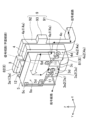
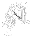
- FIG. 1 is a perspective view of a semiconductor relay according to a first embodiment.
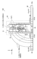
- FIG. 2 is a side view of the semiconductor relay according to the first embodiment as viewed from a direction A shown in FIG.
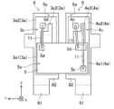
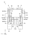
- FIG. 3 is a view showing the first input terminal of the semiconductor relay according to the first embodiment and the second input terminal on which the light emitting element is mounted, as viewed from the direction B shown in FIG. 4A is a diagram of the first output terminal and the second output terminal on which the light-receiving driving element, the first MOSFET element, and the second MOSFET element of the semiconductor relay according to the first embodiment are mounted, as viewed from the direction C shown in FIG. 2.
- FIG. 2 is a side view of the semiconductor relay according to the first embodiment as viewed from a direction A shown in FIG.
- FIG. 4B is a diagram of the light-receiving driver element, the first MOSFET element, the second MOSFET element, the first output terminal, and the second output terminal shown in FIG. 4A, viewed from above in the Z direction.
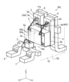
- 4C is a partial exploded perspective view of the light-receiving driving element, the first MOSFET element, the second MOSFET element, the first output terminal, and the second output terminal shown in FIG. 4A.
- FIG. 5 is a perspective view of a light emitting element of the semiconductor relay according to the first embodiment.
- FIG. 6A is a perspective view of a light-receiving driving element of the semiconductor relay according to the first embodiment.
- FIG. 6B is a perspective view of another light-receiving driving element of the semiconductor relay according to the first embodiment.
- FIG. 7 is a perspective view of a first MOSFET element of the semiconductor relay according to the first embodiment.
- FIG. 8 is a perspective view of the electric component unit according to the first embodiment.
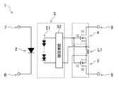
- FIG. 9 is an equivalent circuit diagram of the semiconductor relay according to the first embodiment.
- FIG. 10A is a diagram illustrating a signal path in the semiconductor relay according to the first embodiment.
- FIG. 10B is another diagram showing a signal path in the semiconductor relay according to the first embodiment.
- FIG. 10C is yet another diagram showing a signal path in the semiconductor relay according to the first embodiment.
- FIG. 11 is a view equivalent to FIG. 2 of a semiconductor relay according to a comparative example.
- FIG. 11 is a view equivalent to FIG. 2 of a semiconductor relay according to a comparative example.
- FIG. 12 is a comparison diagram of a signal path in the semiconductor relay according to the first embodiment and a signal path in a semiconductor relay according to a comparative example.
- FIG. 13 is a schematic diagram showing the distribution of parasitic capacitance in a semiconductor relay according to a comparative example.
- FIG. 14 is a schematic diagram for explaining the effect of reducing capacitive coupling between the input side and the output side of the semiconductor relay according to the first embodiment.
- FIG. 15 is a schematic diagram for explaining the effect of reducing capacitive coupling with the ground potential of the semiconductor relay according to the first embodiment.
- FIG. 16 is a perspective view of a semiconductor relay according to the second embodiment. 17 is a side view of the semiconductor relay according to the second embodiment as viewed from the direction D shown in FIG. 16.
- FIG. 18 is a view of the first input terminal and the second input terminal on which the semiconductor relay light emitting element according to the second embodiment is mounted, as viewed from the direction E shown in FIG. 19 is a diagram of the first output terminal and the second output terminal on which the semiconductor relay light-receiving driving element, the first MOSFET element, and the second MOSFET element according to the second embodiment are mounted, viewed from the direction F shown in FIG. 17.
- FIG. FIG. 20 is a schematic diagram comparing the signal path on the output side of the semiconductor relay according to the first embodiment with the signal path on the output side of the semiconductor relay according to the second embodiment.
- FIG. 21 is a diagram comparing the layout relationship between the first input terminal, the second input terminal, and the light-emitting element of the semiconductor relay in the first embodiment and the first input terminal, the second input terminal, and the light-emitting element in the second embodiment.
- FIG. 22 is a diagram corresponding to FIG. 4A and showing the first output terminal and the second output terminal on which the light-receiving driving element, the first MOSFET element, and the second MOSFET element are mounted according to the first modification.
- FIG. 23 is a diagram corresponding to FIG. 4B of the first output terminal and the second output terminal on which the light-receiving driving element, the first MOSFET element, and the second MOSFET element according to the second modification are mounted.
- FIG. 24 is a perspective view of a semiconductor relay according to the third embodiment.
- FIG. 25 is a perspective view of another semiconductor relay according to the third embodiment.
- FIG. 26 is a perspective view of still another semiconductor relay according to the third embodiment.
- FIG. 27 is a perspective view of another semiconductor relay according to the second embodiment.
- FIG. 28 is a perspective view of still another semiconductor relay according to the first embodiment.
- FIG. 29 is a perspective view of still another semiconductor relay according to the third embodiment.
- FIG. 30 is a perspective view of still another semiconductor relay according to the third embodiment.
- FIG. 31 is a perspective view of a semiconductor relay according to the fourth embodiment.
- FIG. 32 is a perspective view of another semiconductor relay according to the fourth embodiment.
- FIG. 33 is a perspective view of still another semiconductor relay according to the fourth embodiment.
- FIG. 1 shows a perspective view of the semiconductor relay according to the present embodiment
- FIG. 2 shows a side view of the semiconductor relay as viewed from the direction A shown in FIG. 1.
- FIG. 3 shows a view of the first input terminal and the second input terminal on which the light-emitting element is mounted as viewed from the direction B shown in FIG. 2
- FIG. 4A shows a view of the first output terminal and the second output terminal on which the light-receiving drive element, the first MOSFET (Metal-Oxide-Semiconductor Field Effect Transistor) element, and the second MOSFET element are mounted as viewed from the direction C shown in FIG. 2.
- FIG. 1 shows a perspective view of the semiconductor relay according to the present embodiment
- FIG. 2 shows a side view of the semiconductor relay as viewed from the direction A shown in FIG. 1.
- FIG. 3 shows a view of the first input terminal and the second input terminal on which the light-emitting element is mounted as viewed from the direction B shown in FIG. 2
- FIG. 4B shows a view of the light-receiving drive element, the first MOSFET element, the second MOSFET element, the first output terminal, and the second output terminal shown in FIG. 4A as viewed from above in the Z direction.
- FIG. 4C shows a partial exploded perspective view of the light-receiving drive element, the first MOSFET element, the second MOSFET element, the first output terminal, and the second output terminal shown in FIG. 4A.
- FIG. 5 shows a perspective view of the light-emitting element
- FIG. 6A shows a perspective view of the light-receiving driving element
- FIG. 7 shows a perspective view of the first MOSFET element.
- the direction in which the light-emitting element 2 and the light-receiving drive element 5 face each other may be referred to as the X direction.
- the direction in which the first output terminal 8 and the second output terminal 9 are aligned may be referred to as the Y direction.
- the Y direction is also the direction in which the first input terminal 6 and the second input terminal 7 are aligned.
- the direction perpendicular to both the X direction and the Y direction may be referred to as the Z direction.
- terms indicating directions such as “top”, “bottom”, “up”, “down”, and “up-down direction” indicate relative directions determined only by the relative positional relationships of the components of the semiconductor relay such as MOSFET elements and light-receiving drive elements, and do not indicate absolute directions such as the vertical direction.
- orthogonal or parallel means orthogonal or parallel, taking into account the processing tolerances and manufacturing tolerances of the components that make up the semiconductor relay 1, as well as the assembly tolerances between the components. It does not mean that the objects being compared are orthogonal or parallel in the strict sense.
- the X direction is also the direction in which the light-receiving driver element 5 is aligned with the first MOSFET element 3 and the second MOSFET element 4.
- the side on which the first MOSFET mounting portion 82 is arranged may be referred to as the top or upper side
- the side on which the first output side external terminal portion 81 is arranged may be referred to as the bottom or lower side.
- the terms "front” and “back” are defined as follows.
- the surface on which the anode electrode 2c is formed is referred to as the front surface 2a
- the surface on which the cathode electrode 2d is formed is referred to as the back surface 2b.
- the surface on which the source electrode 5c and the drain electrode 5d are formed is referred to as the front surface 5a
- the surface opposite the front surface 5a is referred to as the back surface 5b.
- the surfaces on which the first and second gate electrodes 3d, 4d and the first and second source electrodes 3e, 4e are formed are referred to as the front surfaces 3a, 4a, respectively, and the surfaces opposite the front surfaces 3a, 4a are referred to as the back surfaces 3b, 4b.
- the side on which the element is placed or the side on which the wire 11 is connected is referred to as the front surface 6a, 7a, 8a, and 9a
- the surfaces opposite the front surfaces 6a, 7a, 8a, and 9a are referred to as the back surfaces 6b, 7b, 8b, and 9b, respectively.
- the semiconductor relay 1 includes a light-emitting element 2, a light-receiving driving element 5, a first MOSFET element 3, and a second MOSFET element 4.
- the semiconductor relay 1 also includes a first input terminal 6, a second input terminal 7, a first output terminal 8, a second output terminal 9, and a housing 10.
- the light-emitting element 2 is a known LED (Light Emitting Diode) element. As shown in FIG. 5, an anode electrode 2c is formed on the front surface 2a of the light-emitting element, and a cathode electrode 2d is formed on the back surface 2b. The cathode electrode 2d is connected and fixed to the front surface 7a of the light-emitting element mounting portion 72 of the second input terminal 7 via a conductive adhesive such as silver paste. In other words, the cathode electrode 2d is electrically connected to the second input terminal 7.
- a conductive adhesive such as silver paste
- the light-receiving driving element 5 has a light-receiving element 51 and a driving circuit 52 (see FIG. 9).
- the light-receiving element 51 is, for example, a known photodiode arranged in an array.
- a source electrode 5c and a drain electrode 5d are formed on the surface 5a of the light-receiving driving element 5.
- the drain electrode 5d is provided in two locations spaced apart from each other on the surface 5a.
- the light-receiving element 51 is also formed on the surface 5a of the light-receiving driving element 5, but is not shown in the figure for ease of explanation.
- connection conductor 12 is formed on the back surface 5b of the light-receiving driving element 5.
- the connection conductor 12 is formed over the entire back surface 5b of the light-receiving driving element 5.
- the connection conductor 12 is made of one or more conductive films, and is a layered or sheet-shaped conductive member. The configuration and function of the connection conductor 12 will be described later.
- the connection conductor 12 is made of a conductive adhesive sheet that is itself adhered to the back surface 5b of the light-receiving driving element 5.
- the connection conductor 12 may be made of a conductive adhesive sheet that is adhered to the back surface 5b of the light-receiving driving element 5 and a conductive plate that is adhered to the conductive adhesive sheet.
- FIG. 6B is a perspective view of another light-receiving driving element 5 in embodiment 1.
- the light-receiving driving element 5 shown in FIG. 6B has an insulating adhesive sheet 55 provided on the back surface 5b.
- the connecting conductor 12 is provided on the back surface 5b of the light-receiving driving element 5 by being adhered to the insulating adhesive sheet 55.
- the insulating adhesive sheet 55 can increase the adhesion between the light-receiving driving element 5 and the connecting conductor 12, and increase the insulation between the light-receiving driving element 5 and the connecting conductor 12.
- the source electrode 5c of the light-receiving driving element 5 and the first source electrode 3e of the first MOSFET element 3 are electrically connected via a wire 11.
- One of the two drain electrodes 5d, 5d of the light-receiving driving element 5 is electrically connected to the first gate electrode 3d of the first MOSFET element 3 via a wire 11.
- the other of the two drain electrodes 5d, 5d is electrically connected to the second gate electrode 4d of the second MOSFET element 4 via a wire 11.
- the first MOSFET element 3 is formed by forming a known vertical MOSFET on a semiconductor substrate.
- the first MOSFET element 3 is usually composed of multiple vertical MOSFETs connected in series or in parallel. However, it may be a single vertical MOSFET.
- a first gate electrode 3d and a first source electrode 3e are formed on the front surface 3a of the first MOSFET element 3, and a first drain electrode 3f is formed on the back surface 3b.
- the first drain electrode 3f is formed over the entire back surface 3b of the first MOSFET element 3.
- the first cell region 3c is a MOSFET function cell region in which one or more vertical MOSFETs are formed.
- the MOSFET function cell region is a region in which the gate, drain, and source are formed in the semiconductor chip and are connected to the gate electrode, source electrode, and drain electrode, respectively, so that the MOSFET element functions as a MOSFET.
- the first source electrode 3e has a first electrode body portion 3e1 and a first expanded electrode portion 3e2.
- the longitudinal direction of the first electrode body portion 3e1 is the Z direction.
- the first expanded electrode portion 3e2 is formed continuous with the first electrode body portion 3e1.
- the first electrode body portion 3e1 has a portion that overlaps with the light-receiving driving element 5 (see FIGS. 4A and 4C).
- the second MOSFET element 4 has the same structure as the first MOSFET element 3 (see FIG. 7). Therefore, the arrangement and respective shapes of the second gate electrode 4d, second source electrode 4e, and second drain electrode 4f are also the same as those of the first MOSFET element 3. That is, the second source electrode 4e also has a second electrode body portion 4e1 and a second expanded electrode portion 4e2, and the shapes and arrangements of these are the same as those of the first electrode body portion 3e1 and the first expanded electrode portion 3e2, respectively. For example, when viewed along the X direction, the second electrode body portion 4e1 has a portion that overlaps with the light-receiving driving element 5 (see FIGS. 4A and 4C).
- the region on the surface 4a of the second MOSFET element 4 where the second gate electrode 4d and the second source electrode 4e are formed is sometimes called the second cell region 4c.
- the second cell region 4c is a MOSFET function cell region in which one or more vertical MOSFETs are formed, similar to the first cell region 3c.
- a first connector 13 is provided on the surface of the first electrode body 3e1 of the first source electrode 3e.
- a second connector 14 is provided on the surface of the second electrode body 4e1 of the second source electrode 4e.
- the surface 3a of the first MOSFET element 3 may be referred to as the first surface 3a
- the surface 4a of the second MOSFET element 4 may be referred to as the second surface 4a.
- the light receiving drive element 5 is placed on the first surface 3a and the second surface 4a via the first connector 13 and the second connector 14, respectively.
- the portions of the first surface 3a and the second surface 4a on which the light receiving drive element 5 is placed are sometimes referred to as the first mounting portion 3a1 and the second mounting portion 4a1, respectively, and the portions on which the light receiving drive element 5 is not placed are sometimes referred to as the first non-mounting portion 3a2 and the second non-mounting portion 4a2, respectively.
- the first mounting portion 3a1 is provided with a first electrode body portion 3e1 of the first source electrode 3e
- the second mounting portion 4a1 is provided with a second electrode body portion 4e1 of the second source electrode 4e.
- the first non-mounting portion 3a2 is provided with a first expanded electrode portion 3e2 and a first gate electrode 3d of the first source electrode 3e
- the second mounting portion 4a1 is provided with a second expanded electrode portion 4e2 and a second gate electrode 4d of the second source electrode 4e.
- the first drain electrode 3f of the first MOSFET element 3 is fixed to the surface 8a of the first MOSFET mounting portion 82 of the first output terminal 8 by a conductive adhesive such as silver paste.
- the second drain electrode 4f of the second MOSFET element 4 is fixed to the surface 9a of the second MOSFET mounting portion 92 of the second output terminal 9 by a conductive adhesive.
- the first connector 13 and the second connector 14 are each made of a conductor, such as solder.
- the material and shape of the first connector 13 and the second connector 14 are not particularly limited to this, and for example, the first connector 13 and the second connector 14 may be bump electrodes.
- a plurality of first connectors 13 are formed on the surface of the first electrode body 3e1 of the first source electrode 3e, and the first connector 13 is provided.
- a plurality of second connectors 14 may be formed on the surface of the second electrode body 4e1 of the second source electrode 4e.
- the first connector 13 and the second connector 14 are each electrically connected to a connection conductor 12 formed on the back surface 5b of the light-receiving driving element 5 (see Figures 10A to 10C). Furthermore, the first source electrode 3e of the first MOSFET element 3 and the second source electrode 4e of the second MOSFET element 4 are electrically connected via the connection conductor 12 and the first connector 13 and second connector 14.
- connection conductor 12 has first to third connection conductor parts 12a to 12c.
- the first connection conductor part 12a is a part of the connection conductor 12 that is disposed between the light-receiving driving element 5 and the first electrode body part 3e1 of the first source electrode 3e, and is electrically connected to the first connection body 13.
- the second connection conductor part 12b is a part of the connection conductor 12 that is disposed between the light-receiving driving element 5 and the second electrode body part 4e1 of the second source electrode 4e, and is electrically connected to the second connection body 14.
- the third connection conductor part 12c is a part of the connection conductor 12 that electrically connects the first connection conductor part 12a and the second connection conductor part 12b, and overlaps with the light-receiving driving element 5 when viewed along the X direction.
- connection conductor 12 i.e., the first to third connection conductor portions 12a to 12c
- the connection conductor 12 are a single continuous sheet-like conductor.
- this is not particularly limited, and the first to third connection conductor portions 12a to 12c may each have a different shape or thickness.
- the size of the connection conductor 12 is the size required to electrically connect the first connection body 13 and the second connection body 14.
- the width of the connection conductor 12 in the Y direction is the same as or wider than the distance between the first connection body 13 and the second connection body 14 along the Y direction.
- the distance may be the distance D1, D2, or D3 shown in FIG. 4B.
- the distance D1 is the distance in the Y direction between the side surface of the first connection body 13 and the side surface of the adjacent second connection body 14 facing it.
- the distance D2 is the distance in the Y direction between the center line of the first connection body 13 and the center line of the second connection body 14. These center lines are imaginary lines that pass through the centers of the first connection body 13 and the second connection body 14, respectively, and extend in the Z direction.
- Distance D3 is the distance along the Y direction between the side of the first connector 13 that is farthest from the second connector 14 along the Y direction and the side of the second connector 14 that is farthest from the first connector 13 along the Y direction
- the width of the connection conductor 12 in the Z direction is equal to or greater than the length of the first connection body 13 and the second connection body 14 in the Z direction. However, this is not limited to this, and if the connection resistance between the connection conductor 12 and the first connection body 13 and the second connection body 14 is sufficiently low, the width of the connection conductor 12 in the Z direction may be narrower than the length of the first connection body 13 and the second connection body 14 in the Z direction.
- the first input terminal 6 and the second input terminal 7 are each conductive members obtained by processing a copper plate.
- the surface of the copper plate is plated with another metal film, for example, a metal film containing nickel.
- the material of the metal film is not particularly limited to this.
- the light-emitting element 2, first MOSFET element 3, second MOSFET element 4, light-receiving driving element 5, and other components are mounted on a lead frame punched out of a copper plate, and the lead frame and each component are sealed with light-shielding resin 10a.
- the semiconductor relay 1 is then obtained, with the first input terminal 6, second input terminal 7, first output terminal 8, and second output terminal 9 being configured as part of the lead frame. Additionally, light-transmitting resin 10b is filled between the light-receiving driving element 5 and the light-emitting element 2.
- the first input terminal 6 has a first input side external terminal portion 61, a wire connection portion 62, and a branch portion 63.
- the second input terminal 7 has a second input side external terminal portion 71, a light-emitting element mounting portion 72, and branch portions 73a to 73c.
- the first input terminal 6 is arranged next to the second input terminal 7 in the Y direction, but is spaced apart from the second input terminal 7.
- each of the first input terminal 6 and the second input terminal 7 extends downward in the Z direction from one end located inside the housing 10 and is bent near the bottom surface 10L of the housing 10, and the other end extends in the X direction from the side surface of the housing 10 and further protrudes to the outside of the housing 10.
- the portions protruding to the outside of the housing 10 are the first and second input side external terminal portions 61, 71.
- one end of the wire 11 is connected to the surface of the wire connection portion 62, and the other end of the wire 11 is connected to the anode electrode 2c of the light-emitting element 2 as shown in FIG. 3.
- the branch portion 63 protrudes from the wire connection portion 62 in the Y direction different from the X direction and on the opposite side to the second input terminal 7.
- the tip of the branch portion 63 is exposed on the side of the housing 10.
- the branch portion 63 is part of the aforementioned lead frame that remains in the first input terminal 6 when the semiconductor relay 1 is separated.
- the light-emitting element 2 is placed on the surface 7a of the light-emitting element mounting portion 72 of the second input terminal 7.
- the branch portions 73a to 73c are each a part of the lead frame that remains on the second input terminal 7 when the semiconductor relay 1 is separated.
- the tips of the branch portions 73a to 73c protrude in the Y direction, which is different from the X direction, and are exposed on the side of the housing 10.
- the tips of the branch portions 73a and 73b protrude on the side opposite the input terminal 6, and the tip of the branch portion 73c protrudes in the opposite direction to the tips of the branch portions 73a and 73b.
- the parts of the branch portions 73a to 73c that are exposed on the side of the housing 10 may be coated with a resin coating or the like.
- the first output terminal 8 has a first output side external terminal portion 81, a first MOSFET mounting portion 82, and a branch portion 83.
- the second output terminal 9 has a second output side external terminal portion 91, a second MOSFET mounting portion 92, and a branch portion 93.
- each of the first output terminal 8 and the second output terminal 9 extends downward in the Z direction from one end located inside the housing 10 and is bent near the bottom surface of the housing 10, and the other end extends in the Y direction from the side surface of the housing 10 and further protrudes to the outside of the housing 10.
- the part protruding to the outside of the housing 10 is the first output side external terminal portion 81.
- the part protruding to the outside of the housing 10 is the second output side external terminal portion 91.
- the first MOSFET mounting portion 82 and the second MOSFET mounting portion 92 are each disposed inside the housing 10.
- the first MOSFET element 3 is disposed on the surface 8a of the first MOSFET mounting portion 82
- the second MOSFET element 4 is disposed on the surface 9a of the second MOSFET mounting portion 92.
- the first output terminal 8 is disposed next to the second output terminal 9 in the Y direction, but is spaced apart from the second output terminal 9.
- W1 is the distance in the X direction between the respective surfaces 8a, 9a of the first MOSFET mounting portion 82 and the second MOSFET mounting portion 92 and the surface 7a of the light-emitting element mounting portion 72 of the second input terminal 7.
- the first output side external terminal portion 81 faces the first input side external terminal portion 61 of the first input terminal 6 in the Y direction.
- the second output side external terminal portion 91 faces the second input side external terminal portion 71 of the second input terminal 7 in the Y direction.
- the housing 10 seals the first input terminal 6, the second input terminal 7, the first output terminal 8, and the second output terminal 9, and fixes their respective positions. It goes without saying that the light-emitting element 2 mounted on the second input terminal 7, the first MOSFET element 3 mounted on the first output terminal 8, the second MOSFET element 4 mounted on the second output terminal 9, and the light-receiving drive element 5 are also sealed by the housing 10, and their respective positions are fixed. As described above, the first output side external terminal portion 81, the second output side external terminal portion 91, the first input side external terminal portion 61, and the second input side external terminal portion 71 each protrude outside the housing 10.
- the housing 10 is composed of an insulating light-shielding resin 10a and a light-transmitting resin 10b.
- the light-shielding resin 10a is, for example, an epoxy resin containing a black pigment. However, it is not limited to this and may be any material that blocks light.
- the light-transmitting resin 10b is provided between the light-receiving drive element 5 and the light-emitting element 2, and is sealed with the light-shielding resin 10a.
- the light-transmitting resin 10b is, for example, a transparent silicone resin. However, it is not limited to this and may be any insulating resin that is transparent at least to the light emitted by the light-emitting element 2.
- the light-transmitting resin 10b forms an optical coupling portion that optically couples the light-receiving element 51 of the light-receiving drive element 5 and the light-emitting element 2.
- the first input terminal 6 and the second input terminal 7, and the first output terminal 8 and the second output terminal 9 are electrically insulated from each other by the housing 10. Furthermore, the light-emitting element 2 and the light-receiving drive element 5 are optically coupled.
- the semiconductor relay 1 is an input/output isolation type semiconductor relay that turns the output signal on and off by optical coupling while the input signal and the output signal are electrically isolated.
- [Configuration of Electrical Component Unit] 8 shows a perspective view of an electric component unit according to an embodiment, and the electric component unit 100 includes at least a semiconductor relay 1 and a circuit board 40.
- the circuit board 40 is a so-called printed wiring board in which first to third wirings 41, 42, and 43 are formed on the surface of a dielectric substrate 40a made of a dielectric material having a predetermined relative dielectric constant.
- a ground plane 45 (see, for example, FIG. 13) is formed on the lower surface of the dielectric substrate 40a.
- the ground plane 45 is formed over the entire back surface of the dielectric substrate 40a.
- the first to third wirings 41, 42, and 43 and the ground plane 45 are formed by applying copper plating or the like to the front or back surface of the dielectric substrate 40a.
- the first wiring 41 is composed of a pair of parallel wirings 41a, 41b spaced apart in the Y direction and each having a longitudinal direction in the X direction.
- the first wiring 41 is an input signal line for inputting an input signal to the semiconductor relay 1.
- One end of each of the pair of wirings 41a, 41b constituting the first wiring 41 is connected to the first input side external terminal portion 61 of the first input terminal 6 and the second input side external terminal portion 71 of the second input terminal 7, respectively.
- the first input side external terminal portion 61 and the second input side external terminal portion 71 are connected to the first wiring so that their respective lower surfaces are in contact with the respective surfaces of the pair of wirings 41a, 41b constituting the first wiring 41.
- the other end of each of the pair of wirings 41a, 41b constituting the first wiring 41 is an open end.
- the second wiring 42 is composed of a pair of wirings 42a, 42b arranged at an interval in the Y direction, each of which has its longitudinal direction in the Y direction.
- the second wiring 42 is an output signal line for an output signal output from the semiconductor relay 1.
- One end of each of the pair of wirings 42a, 42b constituting the second wiring 42 is connected to the first output side external terminal portion 81 of the first output terminal 8 and the second output side external terminal portion 91 of the second output terminal 9.
- the first output side external terminal portion 81 and the second output side external terminal portion 91 are connected to the second wiring 42 so that their respective lower surfaces are in contact with the respective surfaces of the pair of wirings 42a, 42b constituting the second wiring 42.
- the second wiring 42 is designed as a transmission line with impedance matching to 50 ⁇ .
- the second wiring 42 may be a pair of wirings 42a, 42b that extend elongatedly with the X direction as the longitudinal direction.
- the third wiring 43 includes two wirings 43a, 43b arranged to sandwich the ends of the pair of wirings 41a, 41b constituting the first wiring 41, and a wiring 43c arranged on the opposite side in the X direction to the two wirings 43a, 43b and the second wiring 42.
- the longitudinal direction of each of the three wirings 43a, 43b, 43c is the Y direction.
- the three wirings 43a, 43b, 43c included in the third wiring 43 are also electrically connected to the ground potential via the ground plane 45.
- the third wiring 43 is arranged to be separated from the second wiring 42, which is the output signal line, and to surround the second wiring 42, and plays a role in shielding radiation noise and the like incident on the second wiring 42.
- FIG. 8 shows an example in which only the semiconductor relay 1 is mounted on the circuit board 40, it goes without saying that other elements may also be mounted on the circuit board 40.
- Fig. 9 shows an equivalent circuit diagram of the semiconductor relay. Note that the inductance L1 shown in Fig. 9 is a parasitic inductance between the source (S) of the first MOSFET element 3 and the source (S) of the second MOSFET element 4, and is not an actual component of the semiconductor relay 1.
- the light-emitting element 2 When an input signal is input between the first input terminal 6 and the second input terminal 7, the light-emitting element 2 outputs light of a predetermined wavelength.
- the light generated by the light-emitting element 2 propagates inside the translucent resin 10b and is received by the light-receiving element 51.
- a drive signal which is a voltage signal according to the amount of light emitted by the light emitting element 2, is applied via the wire 11 to the first gate electrode 3d of the first MOSFET element 3 and the second gate electrode 4d of the second MOSFET element 4.
- the light-emitting element 2 When the input signal is no longer input between the first input terminal 6 and the second input terminal 7, the light-emitting element 2 also stops emitting light. In response, the light-receiving element 51 no longer generates a current, and the drive circuit 52 stops.
- the semiconductor relay 1 As described above, the semiconductor relay 1 according to the present embodiment is mounted on the circuit board 40 .
- the semiconductor relay 1 includes at least a light-emitting element 2, a first MOSFET element 3, a second MOSFET element 4, a light-receiving driving element 5, a first input terminal 6, a second input terminal 7, a first output terminal 8, a second output terminal 9, a housing 10, and a connecting conductor 12.
- the light-emitting element 2 is electrically connected to the first input terminal 6 and the second input terminal 7.
- the light receiving drive element 5 has a light receiving element 51 that receives the light output from the light emitting element 2 and outputs a drive signal.
- the first output terminal 8 has a first MOSFET mounting portion 82
- the second output terminal 9 has a second MOSFET mounting portion 82.
- the first MOSFET element 3 has a first gate electrode 3d, a first source electrode 3e, and a first drain electrode 3f.
- the first source electrode 3e is electrically connected to the light-receiving driving element 5, and the first drain electrode 3f is electrically connected to the first output terminal 8.
- the second MOSFET element 4 has a second gate electrode 4d, a second source electrode 4e, and a second drain electrode 4f.
- the second source electrode 4e is electrically connected to the light-receiving driving element 5, and the second drain electrode 4f is electrically connected to the second output terminal 9.
- connection conductor 12 is electrically connected to the first source electrode 3e and the second source electrode 4e.
- the first surface 3a has a first mounting portion 3a1 and a first non-mounting portion 3a2.
- a first source electrode 3e is formed on the first mounting portion 3a1, and the light-receiving driving element 5 is mounted on it.
- a first gate electrode 3d is formed on the first non-mounting portion 3a2, but the light-receiving driving element 5 is not mounted on it.
- the second MOSFET element 4 has a second surface 4a and a second back surface 4b located opposite the second surface 4a and placed on the second MOSFET mounting portion 92.
- the connection conductor 12 has a first connection conductor portion 12a, a second connection conductor portion 12b, and a third connection conductor portion 12c.
- the first connection conductor portion 12a is disposed between the light-receiving driving element 5 and the first source electrode 3e.
- the second connection conductor portion 12b is disposed between the light-receiving driving element 5 and the second source electrode 4e.
- the third connection conductor portion 12c electrically connects the first connection conductor portion 12a and the second connection conductor portion 12b, and has a portion that overlaps with the light-receiving driving element when viewed along the X direction.
- connection conductor 12 is a layer or sheet-like conductive member formed on the back surface 5b of the light-receiving driving element 5.
- FIG. 10A is a diagram showing a signal path in a semiconductor relay.
- FIG. 10B is another diagram showing a signal path in a semiconductor relay.
- FIG. 10C is yet another diagram showing a signal path in a semiconductor relay.
- FIG. 11 is a diagram equivalent to FIG. 2 of a semiconductor relay according to a comparative example.
- FIG. 12 is a comparative diagram of the signal path in the semiconductor relay according to embodiment 1 and the signal path in the semiconductor relay according to the comparative example.
- FIG. 13 is a schematic diagram showing the distribution of parasitic capacitance in the semiconductor relay according to the comparative example.
- FIGS. 10A to 10C and FIG. 12 show a case where a signal is transmitted from the second output terminal 9 to the first output terminal 8.
- FIGS. 11 to 13 and the following FIGS. 14 and 15 the same reference numerals are used for parts similar to those shown in FIGS. 1 to 8, and detailed explanations may be omitted.
- the signal path from the second source electrode 4e of the second MOSFET element 4 to the first source electrode 3e of the first MOSFET element 3 includes a connecting conductor 12.
- connection conductor 12 is a layered or sheet-like conductive member formed over the entire back surface 5b of the light-receiving drive element 5.
- the periphery of the connection conductor 12 roughly overlaps with the periphery of the back surface 5b of the light-receiving drive element 5. Therefore, the signal is transmitted in a state in which it is spread out in a plane in the connection conductor 12 (planar path in Figures 10A and 10B).
- the conventional semiconductor relay 20 shown in FIG. 11 differs from the semiconductor relay 1 of this embodiment in the following respects.
- a third element mounting portion 16 is provided above and along the Z direction, spaced apart from the first output terminal 8 and the second output terminal 9.
- a light-receiving driving element 5 is mounted on a surface 16a of the third element mounting portion 16.
- the light-receiving driving element 5 is disposed above and spaced apart from the first MOSFET element 3 and the second MOSFET element 4 along the Z direction.
- the second source electrode 4e of the second MOSFET element 4 and the first source electrode 3e of the first MOSFET element 3 are connected by two wires 11, and these two wires 11 form a signal path.
- the inductance component related to the signal path between the second source electrode 4e of the second MOSFET element 4 and the first source electrode 3e of the first MOSFET element 3 corresponds to the aforementioned L1.
- the inductance per unit length of the wire 11 along the signal path is roughly proportional to the logarithm of the inverse of the wire diameter.
- the connecting conductor 12 is considered to be a flat conductor, the width of the connecting conductor 12 in the Z direction (the width of the connecting conductor 12 in the direction intersecting the signal path) can be made larger than the width of the connecting conductor 12 in the X direction (the thickness of the flat conductor).
- the inductance per unit length of the connecting conductor 12 along the signal path is less affected by the width of the connecting conductor 12 in the X direction (the thickness of the flat conductor), and is mainly a component proportional to the logarithm of the inverse of the width in the Z direction. Since the width of the connecting conductor 12 in the Z direction is several to several tens of times larger than the wire diameter of the wire 11, the inductance per unit length along the signal path is smaller in the semiconductor relay 1 of this embodiment using the connecting conductor 12 than in the conventional semiconductor relay 20 using the wire 11.
- the semiconductor relay 1 of this embodiment can reduce the parasitic inductance component compared to the conventional semiconductor relay 20, and as a result, insertion loss can be reduced. Furthermore, by reducing the inductance along the signal path, mismatch in the characteristic impedance of the signal path can be reduced. This improves the reflection characteristics in the signal path, and ultimately reduces insertion loss.
- the effect of resonance caused by the stub can be reduced by reducing the capacitive coupling with the ground potential. This will be explained further below.
- the wire 11 connecting the source electrode 5c of the light-receiving drive element 5 and the first source electrode 3e of the first MOSFET element 3 acts as a stub in the high-frequency circuit.
- the resonant frequency fc of the resonant circuit formed by the parasitic capacitance and the wire 11 satisfies the relationship shown in formula (1).
- the second source electrode 4e of the second MOSFET element 4 and the third element mounting portion 16 are connected by a wire 11.
- the driving element 5 and the second MOSFET element 4 are electrically connected via the third element mounting portion 16.
- the wire 11 also acts as a stub.
- C includes the parasitic capacitance between the third element mounting section 16 and the ground potential.
- the light-receiving driving element 5 is disposed above and spaced apart from the first MOSFET element 3 and the second MOSFET element 4 in the Z direction. Therefore, the length of the wire 11 connecting the source electrode 5c of the light-receiving driving element 5 to the first source electrode 3e of the first MOSFET element 3 is longer than that of the wire 11 in the semiconductor relay 1 of this embodiment shown on the right side of FIG. 12. Therefore, the aforementioned inductance value L is also greater in the conventional semiconductor relay 20 than in the semiconductor relay 1 of this embodiment.
- the resonant frequency fc shown in equation (1) is lower in the conventional semiconductor relay 20 than in the semiconductor relay 1 of this embodiment.
- the semiconductor relay 1 of this embodiment has better high frequency characteristics in terms of insertion loss compared to the conventional semiconductor relay 20.
- the light-receiving drive element 5, the first MOSFET element 3, and the second MOSFET element 4 are arranged in the positional relationship shown in Figures 11 and 12.
- parasitic capacitance occurs due to capacitive coupling between the ground potential and the third element mounting section 16.
- parasitic capacitance occurs due to capacitive coupling between the first output terminal 8 and the second output terminal 9 located on the output side, and between the third element mounting section 16 and the first input terminal 6 and the second input terminal 7. Due to these parasitic capacitances, when a signal is transmitted between the first output terminal 8 and the second output terminal 9, the insertion loss described above occurs. In addition, the higher the frequency of the signal, the greater the degree of increase in insertion loss.
- the third element mounting portion 16 shown in Figs. 11 and 12 is omitted, and as shown in Figs. 1 and 2, the light-receiving driving element 5 is mounted across the first mounting portion 3a1 of the first MOSFET element 3 and the second mounting portion 4a1 of the second MOSFET element 4. This makes it possible to reduce both the capacitive coupling with the ground potential and the capacitive coupling between the input side and the output side.
- the coupling capacitance between the stub area and the ground potential can be reduced, reducing insertion loss.
- FIG. 14 is a schematic diagram for explaining the effect of reducing capacitive coupling between the input side and the output side.
- FIG. 15 is a schematic diagram for explaining the effect of reducing capacitive coupling with the ground potential.
- the height H1 in the Z direction of the semiconductor relay 1 of this embodiment can be made lower than the height H2 in the Z direction of the conventional semiconductor relay 20. In other words, a small semiconductor relay 1 with a low profile can be realized.
- the conventional semiconductor relay 20 it is also possible to reduce the size of each of the first MOSFET element 3 and the second MOSFET element 4, thereby achieving miniaturization. For example, by reducing the size in the Z direction of each of the first MOSFET element 3 and the second MOSFET element 4, the height of the semiconductor relay 20 can be reduced.
- the drain resistance contributes greatly to the on-resistance. Reducing the area of the first MOSFET element 3 or the second MOSFET element 4 reduces the drain area and increases the on-resistance. As a result, there is a risk that the high-frequency characteristics of the signal transmitted by the semiconductor relay 20 will deteriorate.
- the light-receiving drive element 5 is mounted across the first mounting portion 3a1 of the first MOSFET element 3 and the second mounting portion 4a1 of the second MOSFET element 4.
- This allows the semiconductor relay 1 to be made lower in height while each of the first MOSFET element 3 and the second MOSFET element 4 maintains a certain level of size.
- the drain area of each of the first MOSFET element 3 and the second MOSFET element 4 does not decrease significantly, an increase in the on-resistance can be suppressed, and a decrease in the high-frequency characteristics of the signal transmitted by the semiconductor relay 1 can be suppressed.
- the electrode area on the output side that contributes to the parasitic capacitance can be significantly reduced.
- the capacitive coupling between the input side and the output side is reduced, and the insertion loss is reduced.
- the distance W2 is the distance in the X direction between the surfaces 8a, 9a, 16a of the first MOSFET mounting portion 82, the second MOSFET mounting portion 92, and the third element mounting portion 16, respectively, and the surface 7a of the light-emitting element mounting portion 72 of the second input terminal 7.
- the parasitic capacitance that occurs between the third element mounting section 16 and the ground potential is eliminated, and the insertion loss caused by this parasitic capacitance is reduced.
- the semiconductor relay 1 further has a connector that connects the connection conductor 12 to the first source electrode 3e of the first MOSFET element 3 and the second source electrode 4e of the second MOSFET element 4.
- the connector includes a first connector 13 and a second connector 14.
- the first connector 13 is a conductor formed on the surface of the first source electrode 3e
- the second connector 14 is a conductor formed on the surface of the second source electrode 4e.
- connection conductor 12 can be reliably connected to the first source electrode 3e and the second source electrode 4e.
- the first connector 13 and the second connector 14 act as buffer materials, thereby reducing the pressure that the first MOSFET element 3 and the second MOSFET element 4 receive during mounting.
- the first connector 13 and the second connector 14 it is possible to avoid the above-mentioned problems and stabilize the characteristics of the first MOSFET element 3 and the second MOSFET element 4. In addition, it is possible to reduce problems during the assembly process and improve the manufacturing yield of the semiconductor relay 1.
- the connecting conductor 12 is preferably formed over the entire back surface 5b of the light receiving drive element 5.
- the width of the connecting conductor 12 in the signal path in the Z direction can be maximized.
- the parasitic inductance component can be reduced, and insertion loss can be reduced.
- the mismatch in the characteristic impedance of the signal path can be reduced, the reflection characteristics within the signal path are improved, and therefore insertion loss can be reduced.
- the width of the connection conductor 12 in the Z direction is equal to or greater than the length of the first connection body 13 and the second connection body 14 in the Z direction.
- connection conductor 12 in the Y direction may be equal to or greater than the distance in the Y direction between the first connector 13 and the second connector 14. In this way, the connection conductor 12 can be reliably electrically connected to the first connector 13 and the second connector 14.
- the first surface 3a of the first MOSFET element 3 has a first cell region 3c in which functional cells as a MOSFET are formed
- the second surface 4a of the second MOSFET element 4 has a second cell region 4c in which functional cells as a MOSFET are formed.
- the first connection conductor portion 12a of the connection conductor 12 is formed away from the first cell region 3c in the Z direction, in other words, in the longitudinal direction of the first MOSFET element 3.
- the second connection conductor portion 12b of the connection conductor 12 is formed away from the second cell region 4c in the Z direction, in other words, in the longitudinal direction of the second MOSFET element 4.
- the regions where the first cell region 3c of the first MOSFET element 3 and the second cell region 4c of the second MOSFET element 4 are not formed, i.e., the regions where no functional cells are formed, are connected and fixed to the connecting conductor 12 via the first connector 13 and the second connector 14. This makes it possible to avoid problems such as changes in the characteristics of the MOSFETs included in the first cell region 3c and the second cell region 4c when mounting the light-receiving driving element 5 on the first surface 3a of the first MOSFET element 3 and the second surface 4a of the second MOSFET element 4.
- the first mounting portion 3a1 and the first gate electrode 3d are arranged side by side in the Z direction.
- the second mounting portion 4a1 and the second gate electrode 4d are arranged side by side in the Z direction.
- the light-emitting element 2 and the light-receiving driving element 5 are arranged facing each other at a predetermined interval along the X direction.
- the light-receiving driving element 5 is arranged between the light-emitting element 2 and the first MOSFET element 3, and between the light-emitting element 2 and the second MOSFET element 4.
- the size of the semiconductor relay 1 can be prevented from increasing in the Z direction, making the semiconductor relay 1 lower-profile and more compact.
- the first input terminal 6 has a first input side external terminal portion 61 that is exposed from the housing 10 to the outside along the underside of the housing 10
- the second input terminal 7 has a second input side external terminal portion 71 that is exposed from the housing 10 to the outside along the underside of the housing 10.
- the first output terminal 8 has a first output side external terminal portion 81 that is exposed from the housing 10 to the outside along the underside of the housing 10, and the second output terminal 9 has a second output side external terminal portion 91 that is exposed from the housing 10 to the outside along the underside of the housing 10.
- a surface-mount type semiconductor relay 1 can be realized in which the underside of the housing 10 serves as the mounting surface.
- the electric component unit 100 includes at least a semiconductor relay 1 and a circuit board 40.
- the circuit board 40 has a first wiring 41, a second wiring (wiring layer) 42, and a third wiring (ground layer) 43 formed on the front surface of a dielectric substrate (dielectric layer) 40a, and a ground plane (ground layer) 45 formed on the rear surface of the dielectric substrate (dielectric layer) 40a.
- the first wiring 41 is connected to the first input terminal 6 and the second input terminal 7 of the semiconductor relay 1.
- the second wiring 42 is connected to the first output terminal 8 and the second output terminal 9 of the semiconductor relay 1.
- the first wiring 41 is an input wiring for a signal input to the semiconductor relay 1
- the second wiring 42 is an output wiring (signal line) for a signal output from the semiconductor relay 1.
- the electrical component unit 100 of this embodiment allows the passing and blocking of signals output from the semiconductor relay 1 to be performed with a simple configuration.
- a third wiring 43 is formed on the upper surface of the circuit board 40 so as to be spaced apart from the second wiring 42 and to surround the second wiring 42.
- the third wiring 43 is electrically connected to a ground plane 45 formed on the lower surface of the circuit board 40, and the ground plane 45 is electrically connected to the ground potential.
- the third wiring 43 connected to ground potential so as to surround the second wiring 42, it is possible to suppress the intrusion of radiation noise and the like into the transmission signal propagating through the second wiring 42. It is also possible to suppress the propagation of radiation noise and the like from the second wiring 42 to other electronic components mounted on the circuit board 40. It is also possible to easily configure a signal transmission circuit that transmits high-frequency signals that are passed or blocked by the semiconductor relay 1.
- Fig. 16 is a perspective view of a semiconductor relay according to embodiment 2.
- Fig. 17 is a side view of the semiconductor relay according to embodiment 2 as viewed from direction D shown in Fig. 16.
- Fig. 18 is a view of a first input terminal and a second input terminal on which a light-emitting element is placed as viewed from direction E shown in Fig. 17.
- Fig. 19 is a view of a first output terminal and a second output terminal on which a light-receiving driving element, a first MOSFET element, and a second MOSFET element are placed as viewed from direction F shown in Fig. 17.
- the semiconductor relay 30 of this embodiment differs from the semiconductor relay 1 of embodiment 1 in the following ways.
- the first mounting portion 3a1 of the first MOSFET element 3 is disposed lower in the Z direction than the first gate electrode 3d.
- the second mounting portion 4a1 of the second MOSFET element 4 is disposed lower in the Z direction than the second gate electrode 4d.
- the first mounting portion 3a1 of the first MOSFET element 3 is disposed higher in the Z direction than the first gate electrode 3d.
- the second mounting portion 4a1 of the second MOSFET element 4 is disposed higher in the Z direction than the second gate electrode 4d.
- the signal path passing through the connection conductor 12 provided on the back surface 5b of the light-receiving drive element 5 passes through a position closer to the first output terminal 8 and the second output terminal 9 than in the semiconductor relay 1 of embodiment 1.
- the signal path can be made even shorter than in the semiconductor relay 1 of embodiment 1, and the parasitic inductance component can be reduced.
- the insertion loss can be further reduced.
- the mismatch in the characteristic impedance of the signal path can be reduced.
- the reflection characteristics in the signal path are improved compared to the case shown in embodiment 1, and therefore the insertion loss can be reduced.
- the light receiving drive element 5 can be positioned closer to the bottom surface of the housing 10, which is the mounting surface for the circuit board 40, compared to the case shown in embodiment 1. This also allows the light emitting element mounting portion 72 to be positioned closer to the bottom surface of the housing 10, compared to the case shown in embodiment 1.
- the second input terminal 7 having the light-emitting element mounting portion 72 can be made low-profile, and accordingly, the first input terminal 6 can also be made low-profile.
- the areas of the portions of the first input terminal 6 and the second input terminal 7 that face the first output terminal 8 and the second output terminal 9 can be made smaller than in the case shown in the first embodiment.
- the area of the portion facing the first output terminal 8 and the second output terminal 9 can be made smaller than in the case shown in embodiment 1.
- the branch portions 73a to 73c provided on the second input terminal 7 are positioned above the light-emitting element 2 in the Z direction.
- the rigidity of the second input terminal 7 in the Z direction can be increased.
- the second input terminal 7 in this embodiment has a light-emitting element mounting portion 72 on which the light-emitting element 2 is mounted, and an exposed portion that is exposed to the outside from the housing 10.
- This exposed portion includes a second input side external terminal portion 71 and branch portions 73a to 73c.
- the second input side external terminal portion 71 is configured to be connected to the circuit board 40, and the branch portions 73a to 73c are configured not to be connected to the circuit board 40.
- the branch portions 73a and 73c are disposed above the light-emitting element 2 in the Z direction.
- the height H7 from the bottom surface 10L of the housing 10 to the top end of the input terminal 7 is lower than the height H5 from the bottom surface 10L of the housing 10 to the top end of the light-receiving drive element 5.
- FIG. 22 is a diagram corresponding to FIG. 4A and showing the first output terminal and the second output terminal on which the light-receiving driving element, the first MOSFET element, and the second MOSFET element are mounted according to the first modification.
- the semiconductor relay 31 of this modified example differs from the semiconductor relay 1 of embodiment 1 in that a single wire 11 is provided to connect the first source electrode 3e of the first MOSFET element 3 and the second source electrode 4e of the second MOSFET element 4.
- the first expanded electrode portion 3e2 of the first source electrode 3e and the second expanded electrode portion 4e2 of the second source electrode 4e are connected by one wire 11, which is the third connector 11a.
- the first expanded electrode portion 3e2 of the first source electrode 3e is formed on the first non-mounted portion 3a2 of the first MOSFET element 3
- the second expanded electrode portion 4e2 of the second source electrode 4e is formed on the second non-mounted portion 4a2 of the second MOSFET element 4.
- the third connector 11a does not overlap the light-receiving driving element 5 and the connecting conductor 12 when viewed in the X direction.
- a wire 11 connecting the first expanded electrode portion 3e2 and the second expanded electrode portion 4e2 is provided at the first output side external terminal portion 81 of the first output terminal 8 and the second output side external terminal portion 91 of the second output terminal 9, closer to the connecting conductor 12 than the connecting conductor 12.
- the inductance along the signal path can be reduced. This makes it possible to reduce insertion loss compared to the case shown in embodiment 1.
- FIG. 23 is a diagram corresponding to FIG. 4B of the first output terminal and the second output terminal on which the light-receiving driving element, the first MOSFET element, and the second MOSFET element according to the second modification are mounted.
- the semiconductor relay 32 of this modified example differs from the semiconductor relay 1 of embodiment 1 in that it has a third connector 15 as a connector that connects the connection conductor 12 to the first source electrode 3e of the first MOSFET element 3 and the second source electrode 4e of the second MOSFET element 4.
- the third connector 15 is a layer or sheet-like conductor provided on the surface of the connection conductor 12, and electrically connects the first connector 13 and the second connector 14 together with the connection conductor 12.
- the widths of the third connector 15 in the Y direction and the Z direction are approximately the same as the widths of the connection conductor 12 in the Y direction and the Z direction.
- the third connector 15 which is a conductor, is provided in parallel with the connection conductor 12, and the first source electrode 3e of the first MOSFET element 3 and the second source electrode 4e of the second MOSFET element 4 are electrically connected via the first connector 13 and the second connector 14. This makes it possible to reduce the inductance along the signal path, and therefore the insertion loss.
- the third connector 15 is layered or sheet-shaped, the connection distance between the light-receiving driver element 5 and the first and second MOSFET elements 3 and 4 in the X direction can be prevented from becoming long. This reduces the inductance along the signal path, and reduces insertion loss.
- the third connector 15 is a conductive die attach film, that is, a semiconductor adhesive film mixed with a conductive filler, but is not limited to this.
- the third connector 15 may be a metal film. If the third connector 15 is a conductive die attach film, there is no need to separately provide an adhesive or the like when connecting to the first connector 13, the second connector 14, or the connecting conductor 12.
- the third connector 15 serves as a buffer material when mounting the light-receiving driver 5 on the first MOSFET element 3 and the second MOSFET element 4, thereby reducing the effect of pressure applied to the first MOSFET element 3 and the second MOSFET element 4 during mounting.
- FIG. 24 is a perspective view of a semiconductor relay according to the third embodiment.
- a semiconductor relay 33 according to the third embodiment shown in FIG. 24 differs from the semiconductor relay 1 according to the first embodiment in the following points.
- the normal direction of the surface 8a of the first MOSFET mounting portion 82 and the surface 9a of the second MOSFET mounting portion 92 is the Z direction. Therefore, the light-receiving driving element 5 and the first MOSFET element 3 and second MOSFET element 4 are stacked along the Z direction. In addition, the normal direction of the surface 5a, which is the light-receiving surface of the light-receiving driving element 5, is also the Z direction.
- the light-receiving drive element 5 and the first and second MOSFET elements 3 and 4 are stacked along the X direction.
- the normal direction of the surface 5a which is the light-receiving surface of the light-receiving drive element 5, is also in the X direction.
- the semiconductor relay of embodiment 3 differs from embodiment 1 in that the normal direction of the surface 5a, which is the light-receiving surface of the light-receiving element, is the Z direction, while the light-emitting surface of the light-emitting element is in the X direction, and they are not arranged opposite each other.
- the respective back surfaces 8b, 9b of the first MOSFET mounting portion 82 and the second MOSFET mounting portion 92 are exposed from the rear surface of the housing 10 and serve as mounting surfaces for the circuit board 40.
- the respective back surfaces 8b, 9b of the first MOSFET mounting portion 82 and the second MOSFET mounting portion 92 correspond to the first output side external terminal portion 81 and the second output side external terminal portion 91 shown in Figures 1 to 4C.
- one branch portion 73 protrudes in the Y direction from the side surface of the light-emitting element mounting portion 72.
- the branch portion 73 is disposed above the light-emitting element 2 in the Z direction.
- the first electrode body portion 3e1 and the second electrode body portion 4e1 have portions that overlap with the light receiving drive element 5.
- the same effects as those achieved by the configuration shown in embodiment 1 can be achieved.
- the parasitic inductance component can be reduced, and as a result, insertion loss can be reduced.
- the mismatch in the characteristic impedance of the signal path can be reduced. This improves the reflection characteristics within the signal path, and ultimately reduces insertion loss.
- degradation of the high-frequency characteristics of the transmission signal can be suppressed, and impedance mismatch in the signal transmission path can be reduced.
- the length of the wire 11 connecting the source electrode 5c of the light-receiving driver element 5 and the first source electrode 3e of the first MOSFET element 3, that is, the member acting as a stub can be shortened. This reduces the characteristic impedance of the signal path, improving the reflection characteristics of the signal within the signal path and ultimately reducing insertion loss.
- insertion loss can be further reduced.
- Embodiments New embodiments can also be created by appropriately combining the components shown in the first to third embodiments and the first to third modifications.
- the third connector 15 shown in the second modification may be applied to the semiconductor relay 30 shown in the second embodiment or the semiconductor relay 33 shown in the third embodiment.
- the first MOSFET element 3 and the second MOSFET element 4 shown in the third modification may be applied to the semiconductor relays 1, 30, and 33 shown in the first to third embodiments. Examples of such combinations are described below.
- FIG. 25 is a perspective view of another semiconductor relay 34 according to embodiment 3.
- the same parts as those in the semiconductor relay 33 according to embodiment 3 shown in FIG. 24 are given the same reference numerals.
- the light-shielding resin 10a of the housing 10 is omitted in order to allow understanding of the configuration of the main parts.
- the surface 2a on which the anode electrode 2c of the light-emitting element 2 is provided and which emits light faces the surface 5a that receives the light of the light-receiving driving element 5 in the Z direction.
- FIG. 26 is a perspective view of yet another semiconductor relay 35 according to embodiment 3.
- the same parts as those in the semiconductor relay 34 shown in FIG. 25 are given the same reference numerals.
- the light-shielding resin 10a of the housing 10 is omitted in order to allow understanding of the configuration of the main parts.
- the semiconductor relay 35 the anode electrode 2c of the light-emitting element 2 is provided, and the surface 2a that emits light faces the X direction, and the surface 5a of the light-receiving driving element 5 that receives light faces the Z direction perpendicular to the X direction.
- the surface 2a of the light-emitting element 2 is perpendicular to the surface 5a of the light-receiving driving element 5, and the light emitted from the surface 2a of the light-emitting element 2 is guided by the light-transmitting resin 10b and received by the surface 5a of the light-receiving driving element 5.
- FIG. 27 is a perspective view of another semiconductor relay 36 according to embodiment 2.
- the same parts as those in the semiconductor relay 30 according to embodiment 2 shown in FIG. 16 are given the same reference numerals.
- the light-shielding resin 10a of the housing 10 is omitted in order to allow understanding of the configuration of the main parts.
- the terminal of the light-receiving driving element 5 connected to the source electrode of the second MOSFET element 4 is located at the upper end of the surface 5a and is connected to the source electrode of the second MOSFET element 4 by the wire 11.
- the wire 11 connecting the light-receiving driving element 5 and the source electrode of the MOSFET element 4 can be shortened, and the frequency of the resonance generated by the stub can be shifted to the higher frequency side.
- FIG. 28 is a perspective view of yet another semiconductor relay 37 according to embodiment 1.
- the same parts as those in the semiconductor relay 1 of embodiment 1 shown in FIG. 1 are given the same reference numerals.
- the light-shielding resin 10a of the housing 10 is omitted in order to allow understanding of the configuration of the main parts.
- the terminal of the light-receiving driving element 5 connected to the source electrode of the second MOSFET element 4 is located at the lower end of the surface 5a, and is connected to the source electrode of the second MOSFET element 4 by the wire 11.
- FIG. 29 is a perspective view of yet another semiconductor relay 38 according to the third embodiment.
- the same parts as those in the semiconductor relay 34 shown in FIG. 25 are given the same reference numerals.
- the light-shielding resin 10a of the housing 10 is omitted in order to allow understanding of the configuration of the main parts.
- the semiconductor relay 38 the surface 2a on which the anode electrode 2c of the light-emitting element 2 is provided and emits light faces the surface 5a of the light-receiving driving element 5 that receives light in the Z direction.
- the output terminals 8, 9 and the MOSFET elements 3, 4 have a shape that is elongated in the X direction. With this configuration, the wire 11 connecting the light-receiving driving element 5 and the source electrode of the MOSFET element 4 can be shortened, and the frequency of the resonance generated by the stub can be shifted to the high frequency side.
- FIG. 30 is a perspective view of yet another semiconductor relay 39 according to the third embodiment.
- the same reference numerals are used for the same parts as those in the semiconductor relay 35 shown in FIG. 26.
- the light-shielding resin 10a of the housing 10 is omitted in order to understand the configuration of the main parts.
- the semiconductor relay 39 the anode electrode 2c of the light-emitting element 2 is provided, and the surface 2a that emits light faces the X direction, and the surface 5a of the light-receiving driving element 5 that receives light faces the Z direction perpendicular to the X direction.
- the surface 2a of the light-emitting element 2 is perpendicular to the surface 5a of the light-receiving driving element 5, and the light emitted from the surface 2a of the light-emitting element 2 is guided by the light-transmitting resin 10b and received by the surface 5a of the light-receiving driving element 5.
- the output terminals 8, 9 and the MOSFET elements 3, 4 have a shape that is elongated in the X direction.
- the mismatch of the characteristic impedance of the signal path can be reduced. This improves the reflection characteristics in the signal path, and thus the insertion loss can be reduced. Furthermore, the deterioration of the high-frequency characteristics of the transmission signal can be suppressed, and the impedance mismatch in the signal transmission path can be reduced.
- the length of the wire 11 connecting the source electrode of the light receiving drive element 5 and the first source electrode of the first MOSFET element 3, that is, the member acting as a stub can be shortened. This reduces the characteristic impedance of the signal path, improving the reflection characteristics of the signal in the signal path, and thus the insertion loss can be reduced.
- the insertion loss can be further reduced. Furthermore, with this configuration, the wire 11 connecting the light receiving drive element 5 and the source electrode of the MOSFET element 4 can be shortened, and the frequency of the resonance generated by the stub can be shifted to the high frequency side.
- the first electrode body 3e1 of the first MOSFET element 3 and the second electrode body 4e1 of the second MOSFET element 4 each have a portion that overlaps with the light-receiving driving element 5 when viewed along the normal direction of the surface 5a of the light-receiving driving element 5.
- the light-receiving driving element 5 overlaps with the first MOSFET element 3 in a planar view.
- the light-receiving driving element 5 overlaps with the second MOSFET element 4 in a planar view.
- the normal N2a of the surface 2a of the light-emitting element 2 intersects with the normal N5a of the surface 5a of the light-receiving drive element 5.
- the normal N2a of the surface 2a of the light-emitting element 2 is non-parallel to the normal N5a of the surface 5a of the light-receiving drive element 5, and is perpendicular to it in this embodiment.
- the surface 5a of the light receiving drive element 5 is parallel to the bottom surface 10L of the housing 10.
- FIG. 32 is a perspective view of another semiconductor relay 30b according to embodiment 4.
- the same parts as those in the semiconductor relay shown in FIG. 1 to FIG. 31 are given the same reference numerals.
- a connecting conductor 12 is provided on the back surface 5b of the light-receiving driving element 5. Specifically, in the semiconductor relay 30b, the first expanded electrode portion 3e2 of the first source electrode 3e and the second expanded electrode portion 4e2 of the second source electrode 4e are connected by the connecting conductor 12.
- the surface 2a of the light-emitting element 2 is parallel to the bottom surface 10L of the housing 10.
- FIG. 33 is a perspective view of yet another semiconductor relay 30c according to embodiment 4.
- the same parts as those in the semiconductor relay shown in FIG. 32 are given the same reference numerals.
- No connecting conductor is provided on the back surface 5b of the light-receiving driving element 5.
- the semiconductor relay 30c the first expanded electrode portion 3e2 of the first source electrode 3e and the second expanded electrode portion 4e2 of the second source electrode 4e are connected by a third connector 11a, which is a single wire.
- the surface 5a of the light receiving drive element 5 is parallel to the bottom surface 10L of the housing 10.
- the semiconductor relays 30a to 30c according to embodiment 4 can reduce the capacitive coupling between the input and output sides, and can reduce insertion loss. Furthermore, the input terminals 6 and 7 of the semiconductor relays 30a to 30c can be made shorter than those of the semiconductor relay according to embodiment 2, and ripples on the input side can be further suppressed.
- a semiconductor relay 1 comprises a first input terminal 6, a second input terminal 7, a light-emitting element 2 electrically connected to the first input terminal 6 and the second input terminal 7, a light-receiving element 5 having a light-receiving element 51 that receives light output from the light-emitting element 2 and outputs a drive signal in response to the received light, a first output terminal 8, a second output terminal 9, a first MOSFET element 3 having a first gate electrode 3d to which the drive signal is input, a first source electrode 3e electrically connected to the light-receiving element, and a first drain electrode 3f electrically connected to the first output terminal 8, a second MOSFET element 4 having a second gate electrode 4d to which the drive signal is input, a second source electrode 4e electrically connected to the light-receiving element, and a second drain electrode 4f electrically connected to the second output terminal 9, and a connecting conductor 12 electrically connected to the first source electrode 3e and
- the first MOSFET element 3 has a first surface 3a on which the first gate electrode 3d and the first source electrode 3e are provided, and a first back surface 3b opposite the first surface 3a.
- the second MOSFET element 4 has a second surface 4a on which the second gate electrode 4d and the second source electrode 4e are provided, and a second back surface 4b opposite the second surface 4a.
- the first surface 3a of the first MOSFET element 3 has a first mounting portion 3a1 on which the first source electrode 3e is provided and on which the light-receiving driving element 5 is mounted, and a first non-mounting portion 3a2 on which the first gate electrode 3d is provided and on which the light-receiving driving element 5 is not mounted.
- the second surface 4a of the second MOSFET element 4 has a second mounting portion 4a1 on which the second source electrode 4e is provided and on which the light-receiving driving element 5 is mounted, and a second non-mounting portion 4a2 on which the second gate electrode 4d is provided and on which the light-receiving driving element 5 is not mounted.
- the first MOSFET element 3 and the second MOSFET element 4 are located in a first direction (X direction) from the light-receiving driving element 5 so as to face a back surface 5b of the light-receiving driving element 5.
- the first MOSFET element 3 is located in a second direction (Y direction) from the second MOSFET element 4 that is perpendicular to the first direction (X direction).
- the connection conductor 12 has a first connection conductor portion 12a that overlaps with the first MOSFET element 3 when viewed in the first direction (X direction), a second connection conductor portion 12b that overlaps with the second MOSFET element 4 when viewed in the first direction (X direction), and a third connection conductor portion 12c that electrically connects the first connection conductor portion 12a to the second connection conductor portion 12b and does not overlap with the first MOSFET element 3 and the second MOSFET element 4 when viewed in the first direction (X direction).
- the connection conductor 12 is provided on the back surface 5b of the light-receiving driving element 5.
- connection conductor 12 may be provided over the entire back surface 5b of the light receiving drive element 5.
- the light-receiving driving element 5 may have an insulating adhesive sheet 55 provided on the back surface 5b of the light-receiving driving element 5 to adhere the connection conductor 12 to the back surface 5b of the light-receiving driving element 5.
- the semiconductor relay includes a first connector 13 provided on a surface of the first source electrode 3e, a second connector 14 provided on a surface of the second source electrode 4e,
- the first connection body 13 electrically connects the first source electrode 3e to the first connection conductor portion 12a of the connection conductor 12.
- the second connection body 14 electrically connects the second source electrode 4e to the second connection conductor portion 12b of the connection conductor 12.
- the first connector 13 and the second connector 14 may be aligned along the second direction (Y direction).
- the width of the connection conductor 12 in the second direction (Y direction) is equal to or greater than the distance between the first connector 13 and the second connector 14 in the second direction (Y direction).
- the first MOSFET element 3 may have a first MOSFET functional cell (first cell region 3c).
- the second MOSFET element 4 may have a second MOSFET functional cell.
- the first connector 13 does not overlap the first MOSFET functional cell (first cell region 3c) when viewed in the first direction (X direction).
- the second connector 14 does not overlap the second MOSFET functional cell (second cell region 4c) when viewed in the first direction (X direction).
- the semiconductor relay may further include a third connection body 11a that is connected to the first source electrode 3e and the second source electrode 4e and does not overlap the light receiving drive element 5 and the connection conductor 12 when viewed in the first direction (X direction).
- the semiconductor relay may further include a housing 10 that accommodates the first input terminal 6, the second input terminal 7, the light-emitting element 2, the light-receiving driving element 5, the first output terminal 8, the second output terminal 9, the first MOSFET element 3, the second MOSFET element 4, and the connecting conductor 12.
- the first direction (X direction), the second direction (Y direction), and the up-down direction (Z direction) are perpendicular to each other.
- the first input terminal 6 has a first input side external terminal portion 61 exposed to the outside of the housing 10 along the lower surface of the housing 10.
- the second input terminal 7 has a second input side external terminal portion 71 exposed to the outside of the housing 10 along the lower surface of the housing 10.
- the first output terminal 8 has a first output side external terminal portion 81 exposed to the outside of the housing 10 along the lower surface of the housing 10, and a first MOSFET mounting portion 82 on which the first MOSFET element 3 is mounted.
- the second output terminal 9 has a second output side external terminal portion 91 exposed to the outside of the housing 10 along the lower surface of the housing 10, and a second MOSFET mounting portion 92 on which the second MOSFET element 4 is mounted.
- the first input side external terminal portion 61, the second input side external terminal portion 71, the first output side external terminal portion 81, and the second output side external terminal portion 91 are located below the light receiving drive element 5.
- the first mounting portion 3a1 of the first surface 3a of the first MOSFET element 3 may be located below the first gate electrode 3d.
- the second mounting portion 4a1 of the second surface 4a of the second MOSFET element 4 may be located below the second gate electrode 4d.
- the second input terminal 7 may further have a light-emitting element mounting portion 72 on which the light-emitting element 2 is mounted, and a branch portion 73 exposed to the outside from the housing 10 and located above the second input side external terminal portion 71.
- the branch portion 73 is exposed from the housing 10 in a direction different from the first direction (X direction).
- the light-emitting element 2 and the light-receiving driving element 5 may face each other at a distance along the first direction (X direction).
- the light-receiving driving element 5 is disposed between the light-emitting element 2 and the first MOSFET element 3 and between the light-emitting element and the second MOSFET element.
- the semiconductor relay disclosed herein can be made compact and has reduced insertion loss, making it useful as an element for passing and blocking high-frequency signals.
Landscapes
- Photo Coupler, Interrupter, Optical-To-Optical Conversion Devices (AREA)
- Electronic Switches (AREA)
Priority Applications (3)
| Application Number | Priority Date | Filing Date | Title |
|---|---|---|---|
| EP24770563.5A EP4682960A1 (en) | 2023-03-14 | 2024-03-01 | Semiconductor relay and electric component unit comprising same |
| JP2025506707A JPWO2024190452A1 (https=) | 2023-03-14 | 2024-03-01 | |
| CN202480016276.0A CN120883754A (zh) | 2023-03-14 | 2024-03-01 | 半导体继电器和具备该半导体继电器的电气部件单元 |
Applications Claiming Priority (2)
| Application Number | Priority Date | Filing Date | Title |
|---|---|---|---|
| JP2023-039857 | 2023-03-14 | ||
| JP2023039857 | 2023-03-14 |
Publications (1)
| Publication Number | Publication Date |
|---|---|
| WO2024190452A1 true WO2024190452A1 (ja) | 2024-09-19 |
Family
ID=92755016
Family Applications (1)
| Application Number | Title | Priority Date | Filing Date |
|---|---|---|---|
| PCT/JP2024/007704 Ceased WO2024190452A1 (ja) | 2023-03-14 | 2024-03-01 | 半導体リレー及びこれを備えた電気部品ユニット |
Country Status (5)
| Country | Link |
|---|---|
| EP (1) | EP4682960A1 (https=) |
| JP (1) | JPWO2024190452A1 (https=) |
| CN (1) | CN120883754A (https=) |
| TW (1) | TWI885766B (https=) |
| WO (1) | WO2024190452A1 (https=) |
Citations (5)
| Publication number | Priority date | Publication date | Assignee | Title |
|---|---|---|---|---|
| JP2011166077A (ja) * | 2010-02-15 | 2011-08-25 | Panasonic Electric Works Co Ltd | 半導体リレー |
| JP2015050281A (ja) * | 2013-08-30 | 2015-03-16 | 株式会社東芝 | 光結合装置 |
| JP2020088091A (ja) * | 2018-11-21 | 2020-06-04 | 株式会社東芝 | 光結合装置 |
| JP2020096105A (ja) * | 2018-12-13 | 2020-06-18 | 株式会社東芝 | 光結合装置およびその実装部材 |
| JP2021125670A (ja) * | 2020-02-10 | 2021-08-30 | 株式会社東芝 | 光結合装置 |
Family Cites Families (6)
| Publication number | Priority date | Publication date | Assignee | Title |
|---|---|---|---|---|
| JPH11163394A (ja) * | 1997-11-28 | 1999-06-18 | Matsushita Electric Works Ltd | 半導体リレー |
| JP2005347373A (ja) * | 2004-06-01 | 2005-12-15 | Nec Compound Semiconductor Devices Ltd | 半導体リレー、半導体装置及びその製造方法 |
| JP2008244972A (ja) * | 2007-03-28 | 2008-10-09 | Advantest Corp | 半導体リレー |
| TWM564290U (zh) * | 2018-04-25 | 2018-07-21 | 睿宇興業有限公司 | 光繼電器 |
| JP7273701B2 (ja) * | 2019-12-04 | 2023-05-15 | 株式会社東芝 | フォトリレー |
| JP7724469B2 (ja) * | 2020-08-05 | 2025-08-18 | パナソニックIpマネジメント株式会社 | 半導体リレーモジュール |
-
2024
- 2024-03-01 JP JP2025506707A patent/JPWO2024190452A1/ja active Pending
- 2024-03-01 EP EP24770563.5A patent/EP4682960A1/en active Pending
- 2024-03-01 WO PCT/JP2024/007704 patent/WO2024190452A1/ja not_active Ceased
- 2024-03-01 CN CN202480016276.0A patent/CN120883754A/zh active Pending
- 2024-03-01 TW TW113107462A patent/TWI885766B/zh active
Patent Citations (6)
| Publication number | Priority date | Publication date | Assignee | Title |
|---|---|---|---|---|
| JP2011166077A (ja) * | 2010-02-15 | 2011-08-25 | Panasonic Electric Works Co Ltd | 半導体リレー |
| JP5491894B2 (ja) | 2010-02-15 | 2014-05-14 | パナソニック株式会社 | 半導体リレー |
| JP2015050281A (ja) * | 2013-08-30 | 2015-03-16 | 株式会社東芝 | 光結合装置 |
| JP2020088091A (ja) * | 2018-11-21 | 2020-06-04 | 株式会社東芝 | 光結合装置 |
| JP2020096105A (ja) * | 2018-12-13 | 2020-06-18 | 株式会社東芝 | 光結合装置およびその実装部材 |
| JP2021125670A (ja) * | 2020-02-10 | 2021-08-30 | 株式会社東芝 | 光結合装置 |
Non-Patent Citations (1)
| Title |
|---|
| See also references of EP4682960A1 |
Also Published As
| Publication number | Publication date |
|---|---|
| TW202504122A (zh) | 2025-01-16 |
| TWI885766B (zh) | 2025-06-01 |
| JPWO2024190452A1 (https=) | 2024-09-19 |
| CN120883754A (zh) | 2025-10-31 |
| EP4682960A1 (en) | 2026-01-21 |
Similar Documents
| Publication | Publication Date | Title |
|---|---|---|
| US6807065B2 (en) | Multilayer printed circuit board | |
| JP7502983B2 (ja) | 光モジュール | |
| CN112183396A (zh) | 显示组件和显示装置 | |
| JP7063695B2 (ja) | 光モジュール | |
| US12342452B2 (en) | Circuit board and electronic device | |
| JP4828103B2 (ja) | 光送受信モジュール | |
| CN113013262B (zh) | 光模块 | |
| JP7435751B2 (ja) | 多層基板 | |
| WO2024190452A1 (ja) | 半導体リレー及びこれを備えた電気部品ユニット | |
| CN112491479B (zh) | 光接收装置 | |
| CN107251659A (zh) | 柔性基板、带柔性基板的部件以及带柔性基板的部件的制造方法 | |
| EP4439683A1 (en) | Semiconductor relay and electric circuit comprising same | |
| CN220456625U (zh) | 电路基板 | |
| JP2023180383A (ja) | 半導体リレー及びそれを備えた半導体リレーモジュール | |
| WO2023189918A1 (ja) | 半導体リレー及びそれを備えた半導体リレーモジュール | |
| JP2019186379A (ja) | 光モジュール | |
| US20250309208A1 (en) | Semiconductor device | |
| CN215641961U (zh) | 迷你光发射组件和光模块 | |
| JP4127652B2 (ja) | 光モジュール | |
| JP7633841B2 (ja) | 半導体発光装置および光サブアセンブリ | |
| JP2026045791A (ja) | 半導体装置 | |
| WO2025057711A1 (ja) | 半導体リレー | |
| JP5515769B2 (ja) | 光伝送モジュール及び筐体 | |
| JP2023176187A (ja) | 半導体装置 |
Legal Events
| Date | Code | Title | Description |
|---|---|---|---|
| 121 | Ep: the epo has been informed by wipo that ep was designated in this application |
Ref document number: 24770563 Country of ref document: EP Kind code of ref document: A1 |
|
| WWE | Wipo information: entry into national phase |
Ref document number: 2025506707 Country of ref document: JP |
|
| WWE | Wipo information: entry into national phase |
Ref document number: 202480016276.0 Country of ref document: CN |
|
| WWE | Wipo information: entry into national phase |
Ref document number: 2024770563 Country of ref document: EP |
|
| NENP | Non-entry into the national phase |
Ref country code: DE |
|
| WWP | Wipo information: published in national office |
Ref document number: 202480016276.0 Country of ref document: CN |
|
| ENP | Entry into the national phase |
Ref document number: 2024770563 Country of ref document: EP Effective date: 20251014 |
|
| ENP | Entry into the national phase |
Ref document number: 2024770563 Country of ref document: EP Effective date: 20251014 |
|
| ENP | Entry into the national phase |
Ref document number: 2024770563 Country of ref document: EP Effective date: 20251014 |
|
| ENP | Entry into the national phase |
Ref document number: 2024770563 Country of ref document: EP Effective date: 20251014 |
|
| ENP | Entry into the national phase |
Ref document number: 2024770563 Country of ref document: EP Effective date: 20251014 |