WO2024190344A1 - 半導体装置 - Google Patents
半導体装置 Download PDFInfo
- Publication number
- WO2024190344A1 WO2024190344A1 PCT/JP2024/006344 JP2024006344W WO2024190344A1 WO 2024190344 A1 WO2024190344 A1 WO 2024190344A1 JP 2024006344 W JP2024006344 W JP 2024006344W WO 2024190344 A1 WO2024190344 A1 WO 2024190344A1
- Authority
- WO
- WIPO (PCT)
- Prior art keywords
- well
- trench
- electrode
- region
- semiconductor device
- Prior art date
- Legal status (The legal status is an assumption and is not a legal conclusion. Google has not performed a legal analysis and makes no representation as to the accuracy of the status listed.)
- Ceased
Links
Images








Classifications
-
- H—ELECTRICITY
- H10—SEMICONDUCTOR DEVICES; ELECTRIC SOLID-STATE DEVICES NOT OTHERWISE PROVIDED FOR
- H10D—INORGANIC ELECTRIC SEMICONDUCTOR DEVICES
- H10D12/00—Bipolar devices controlled by the field effect, e.g. insulated-gate bipolar transistors [IGBT]
- H10D12/211—Gated diodes
- H10D12/212—Gated diodes having PN junction gates, e.g. field controlled diodes
-
- H—ELECTRICITY
- H10—SEMICONDUCTOR DEVICES; ELECTRIC SOLID-STATE DEVICES NOT OTHERWISE PROVIDED FOR
- H10D—INORGANIC ELECTRIC SEMICONDUCTOR DEVICES
- H10D8/00—Diodes
- H10D8/60—Schottky-barrier diodes
- H10D8/605—Schottky-barrier diodes of the trench conductor-insulator-semiconductor barrier type, e.g. trench MOS barrier Schottky rectifiers [TMBS]
-
- H—ELECTRICITY
- H10—SEMICONDUCTOR DEVICES; ELECTRIC SOLID-STATE DEVICES NOT OTHERWISE PROVIDED FOR
- H10D—INORGANIC ELECTRIC SEMICONDUCTOR DEVICES
- H10D62/00—Semiconductor bodies, or regions thereof, of devices having potential barriers
- H10D62/10—Shapes, relative sizes or dispositions of the regions of the semiconductor bodies; Shapes of the semiconductor bodies
- H10D62/102—Constructional design considerations for preventing surface leakage or controlling electric field concentration
- H10D62/103—Constructional design considerations for preventing surface leakage or controlling electric field concentration for increasing or controlling the breakdown voltage of reverse-biased devices
-
- H—ELECTRICITY
- H10—SEMICONDUCTOR DEVICES; ELECTRIC SOLID-STATE DEVICES NOT OTHERWISE PROVIDED FOR
- H10D—INORGANIC ELECTRIC SEMICONDUCTOR DEVICES
- H10D62/00—Semiconductor bodies, or regions thereof, of devices having potential barriers
- H10D62/10—Shapes, relative sizes or dispositions of the regions of the semiconductor bodies; Shapes of the semiconductor bodies
- H10D62/102—Constructional design considerations for preventing surface leakage or controlling electric field concentration
- H10D62/103—Constructional design considerations for preventing surface leakage or controlling electric field concentration for increasing or controlling the breakdown voltage of reverse-biased devices
- H10D62/105—Constructional design considerations for preventing surface leakage or controlling electric field concentration for increasing or controlling the breakdown voltage of reverse-biased devices by having particular doping profiles, shapes or arrangements of PN junctions; by having supplementary regions, e.g. junction termination extension [JTE]
- H10D62/106—Constructional design considerations for preventing surface leakage or controlling electric field concentration for increasing or controlling the breakdown voltage of reverse-biased devices by having particular doping profiles, shapes or arrangements of PN junctions; by having supplementary regions, e.g. junction termination extension [JTE] having supplementary regions doped oppositely to or in rectifying contact with regions of the semiconductor bodies, e.g. guard rings with PN or Schottky junctions
-
- H—ELECTRICITY
- H10—SEMICONDUCTOR DEVICES; ELECTRIC SOLID-STATE DEVICES NOT OTHERWISE PROVIDED FOR
- H10D—INORGANIC ELECTRIC SEMICONDUCTOR DEVICES
- H10D62/00—Semiconductor bodies, or regions thereof, of devices having potential barriers
- H10D62/10—Shapes, relative sizes or dispositions of the regions of the semiconductor bodies; Shapes of the semiconductor bodies
- H10D62/124—Shapes, relative sizes or dispositions of the regions of semiconductor bodies or of junctions between the regions
- H10D62/126—Top-view geometrical layouts of the regions or the junctions
-
- H—ELECTRICITY
- H10—SEMICONDUCTOR DEVICES; ELECTRIC SOLID-STATE DEVICES NOT OTHERWISE PROVIDED FOR
- H10D—INORGANIC ELECTRIC SEMICONDUCTOR DEVICES
- H10D8/00—Diodes
- H10D8/01—Manufacture or treatment
- H10D8/051—Manufacture or treatment of Schottky diodes
-
- H—ELECTRICITY
- H10—SEMICONDUCTOR DEVICES; ELECTRIC SOLID-STATE DEVICES NOT OTHERWISE PROVIDED FOR
- H10D—INORGANIC ELECTRIC SEMICONDUCTOR DEVICES
- H10D8/00—Diodes
- H10D8/60—Schottky-barrier diodes
-
- H—ELECTRICITY
- H10—SEMICONDUCTOR DEVICES; ELECTRIC SOLID-STATE DEVICES NOT OTHERWISE PROVIDED FOR
- H10W—GENERIC PACKAGES, INTERCONNECTIONS, CONNECTORS OR OTHER CONSTRUCTIONAL DETAILS OF DEVICES COVERED BY CLASS H10
- H10W10/00—Isolation regions in semiconductor bodies between components of integrated devices
-
- H—ELECTRICITY
- H10—SEMICONDUCTOR DEVICES; ELECTRIC SOLID-STATE DEVICES NOT OTHERWISE PROVIDED FOR
- H10W—GENERIC PACKAGES, INTERCONNECTIONS, CONNECTORS OR OTHER CONSTRUCTIONAL DETAILS OF DEVICES COVERED BY CLASS H10
- H10W10/00—Isolation regions in semiconductor bodies between components of integrated devices
- H10W10/01—Manufacture or treatment
-
- H—ELECTRICITY
- H10—SEMICONDUCTOR DEVICES; ELECTRIC SOLID-STATE DEVICES NOT OTHERWISE PROVIDED FOR
- H10W—GENERIC PACKAGES, INTERCONNECTIONS, CONNECTORS OR OTHER CONSTRUCTIONAL DETAILS OF DEVICES COVERED BY CLASS H10
- H10W10/00—Isolation regions in semiconductor bodies between components of integrated devices
- H10W10/01—Manufacture or treatment
- H10W10/011—Manufacture or treatment of isolation regions comprising dielectric materials
-
- H—ELECTRICITY
- H10—SEMICONDUCTOR DEVICES; ELECTRIC SOLID-STATE DEVICES NOT OTHERWISE PROVIDED FOR
- H10W—GENERIC PACKAGES, INTERCONNECTIONS, CONNECTORS OR OTHER CONSTRUCTIONAL DETAILS OF DEVICES COVERED BY CLASS H10
- H10W10/00—Isolation regions in semiconductor bodies between components of integrated devices
- H10W10/10—Isolation regions comprising dielectric materials
-
- H—ELECTRICITY
- H10—SEMICONDUCTOR DEVICES; ELECTRIC SOLID-STATE DEVICES NOT OTHERWISE PROVIDED FOR
- H10D—INORGANIC ELECTRIC SEMICONDUCTOR DEVICES
- H10D12/00—Bipolar devices controlled by the field effect, e.g. insulated-gate bipolar transistors [IGBT]
- H10D12/01—Manufacture or treatment
- H10D12/021—Manufacture or treatment of gated diodes, e.g. field-controlled diodes [FCD]
-
- H—ELECTRICITY
- H10—SEMICONDUCTOR DEVICES; ELECTRIC SOLID-STATE DEVICES NOT OTHERWISE PROVIDED FOR
- H10D—INORGANIC ELECTRIC SEMICONDUCTOR DEVICES
- H10D62/00—Semiconductor bodies, or regions thereof, of devices having potential barriers
- H10D62/80—Semiconductor bodies, or regions thereof, of devices having potential barriers characterised by the materials
- H10D62/83—Semiconductor bodies, or regions thereof, of devices having potential barriers characterised by the materials being Group IV materials, e.g. B-doped Si or undoped Ge
- H10D62/832—Semiconductor bodies, or regions thereof, of devices having potential barriers characterised by the materials being Group IV materials, e.g. B-doped Si or undoped Ge being Group IV materials comprising two or more elements, e.g. SiGe
- H10D62/8325—Silicon carbide
Definitions
- the present invention relates to a semiconductor device.
- a semiconductor device includes a semiconductor substrate, a semiconductor layer formed on the semiconductor substrate, an anode electrode formed on the semiconductor layer, and a cathode electrode formed on the semiconductor substrate on the side opposite the semiconductor layer (see, for example, Patent Document 1).
- a semiconductor device includes a semiconductor substrate having a first conductivity type semiconductor substrate surface and a substrate back surface opposite to the substrate surface, a semiconductor layer of a first conductivity type formed on the substrate surface and having a surface, a first electrode formed on the surface of the semiconductor layer, a second electrode formed on the substrate back surface, a plurality of trenches extending from the surface of the semiconductor layer in a thickness direction of the semiconductor layer and in a first direction perpendicular to the thickness direction of the semiconductor layer, and spaced apart in a second direction perpendicular to the thickness direction of the semiconductor layer and the first direction, an insulating layer provided to cover the bottom wall and side wall of each of the trenches, and a third electrode formed in the insulating layer and in contact with the first electrode.
- the well region extending in a direction intersecting the first direction and being one of a plurality of well regions spaced apart in the first direction, the well region having a well surface forming a portion of the surface of the semiconductor layer and a well end portion contacting the insulating layer of the trench, the well surface being one of a plurality of well surfaces, the surface of the semiconductor layer forming an ohmic contact with the first electrode at the well surface, and the surface of the semiconductor layer forming a Schottky contact with the first electrode at an exposed surface located between the plurality of well surfaces.
- the semiconductor device disclosed herein can easily adjust the characteristics of reducing the forward voltage drop and suppressing the leakage current.
- FIG. 1 is a schematic plan view of a semiconductor device according to an embodiment.
- FIG. 2 is a schematic plan view of a semiconductor layer of the semiconductor device of FIG.
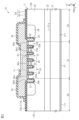
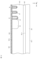
- FIG. 3 is a schematic cross-sectional view of the semiconductor device taken along line F3-F3 in FIG.
- FIG. 4 is a schematic cross-sectional view showing an enlarged view of the periphery of the trench in FIG.
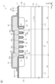
- FIG. 5 is a schematic cross-sectional view of the semiconductor device taken along line F5-F5 in FIG.
- FIG. 6 is a schematic cross-sectional view of the semiconductor device taken along line F6-F6 in FIG.
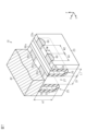
- FIG. 7 is a schematic cross-sectional perspective view showing the surface of a semiconductor layer and the shape of a trench in the semiconductor device of FIG.
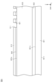
- FIG. 8A to 8C are schematic cross-sectional views showing a manufacturing process of a semiconductor device.
- FIG. 9 is a schematic cross-sectional view showing a manufacturing process subsequent to FIG.
- FIG. 10 is a schematic cross-sectional view showing a manufacturing process subsequent to FIG.
- FIG. 11 is a schematic cross-sectional view showing a manufacturing process subsequent to FIG.
- FIG. 12 is a schematic cross-sectional view showing a manufacturing process subsequent to FIG.
- FIG. 13 is a schematic cross-sectional view showing a manufacturing process subsequent to FIG.
- FIG. 14 is a schematic cross-sectional view showing a manufacturing process subsequent to FIG.
- FIG. 15 is a schematic cross-sectional view showing a manufacturing process subsequent to FIG.
- FIG. 16 is a schematic cross-sectional view showing a manufacturing process subsequent to FIG.
- FIG. 17 is a schematic cross-sectional view showing a manufacturing process subsequent to FIG.
- FIG. 18 is a schematic plan view of a semiconductor layer showing the arrangement of well regions
- FIG. 1 shows a schematic planar structure of the semiconductor device 10.
- Figure 2 shows a schematic planar structure of a semiconductor chip 11, described later, of the semiconductor device 10 of Figure 1.
- Figure 3 shows a schematic cross-sectional structure taken along line F3-F3 in Figure 2.
- Figure 4 is an enlarged cross-sectional view of the range indicated by arrow F4 in Figure 3.
- the surface protection layer 70 described below is indicated with cross-hatched lines.
- the surface insulating layer 60, the anode electrode 42, and the surface protection layer 70 described below are omitted, and the isolation trench 24 and the trench 25 described below are indicated with cross-hatched lines.
- FIG. 3 and FIG. 4 for convenience, some of the hatched lines of the semiconductor device 10 are omitted.
- planar view refers to viewing the semiconductor device 10 in the Z-axis direction of the mutually orthogonal XYZ axes shown in FIG. 1.
- the +Z direction is defined as up, the -Z direction as down, the +X direction as right, and the -X direction as left.
- planear view refers to viewing the semiconductor device 10 from above along the Z-axis.
- the semiconductor device 10 is a semiconductor rectifier. As shown in FIG. 1, the semiconductor device 10 includes a semiconductor chip 11.
- the semiconductor chip 11 is formed of a material containing, for example, silicon (Si).
- the material constituting the semiconductor chip 11 is not limited to Si and is arbitrary.
- the semiconductor chip 11 is formed in a flat plate shape.
- the semiconductor chip 11 includes a chip front surface 11s and a chip back surface 11r (see FIG. 3). Furthermore, the semiconductor chip 11 includes first to fourth chip side surfaces 12A to 12D that connect the chip front surface 11s and the chip back surface 11r.
- the shape of the semiconductor chip 11 in a plan view is rectangular.
- the first chip side 12A and the second chip side 12B extend along the X-axis direction
- the third chip side 12C and the fourth chip side 12D extend along the Y-axis direction.
- the first chip side 12A and the second chip side 12B are arranged to face the Y-axis direction
- the third chip side 12C and the fourth chip side 12D are arranged to face the X-axis direction.
- the semiconductor device 10 includes a semiconductor substrate 21 formed on the semiconductor chip 11 near the chip back surface 11r.
- the semiconductor substrate 21 has a substrate surface 21s and a substrate back surface 21r opposite the substrate surface 21s.
- the substrate surface 21s faces the same side as the chip surface 11s, and the substrate back surface 21r faces the same side as the chip back surface 11r.
- the semiconductor substrate 21 has an electrical resistivity of, for example, 0.5 m ⁇ cm or more and 3 m ⁇ cm or less.
- the semiconductor substrate 21 has an n-type impurity concentration of, for example, 1 ⁇ 10 18 cm ⁇ 3 or more and 1 ⁇ 10 21 cm ⁇ 3 or less.
- the semiconductor substrate 21 has a thickness of 5 ⁇ m or more and 300 ⁇ m or less. In one example, the thickness of the semiconductor substrate 21 is 50 ⁇ m or more and 300 ⁇ m or less.
- the semiconductor substrate 21 is formed of an n-type semiconductor substrate.
- a Si substrate is used as the semiconductor substrate 21, for example.
- the constituent material of the semiconductor substrate 21 is not limited to Si and is arbitrary. In one example, the constituent material of the semiconductor substrate 21 may be silicon carbide (SiC).
- the semiconductor device 10 includes a cathode electrode 41 formed on the substrate back surface 21r of the semiconductor substrate 21.
- the cathode electrode 41 is formed over the entire substrate back surface 21r.
- the cathode electrode 41 is electrically connected to the semiconductor substrate 21.
- the cathode electrode 41 forms an ohmic contact with the semiconductor substrate 21 (substrate back surface 21r).
- the cathode electrode 41 constitutes the chip back surface 11r.
- the cathode electrode 41 corresponds to the "second electrode.”
- the cathode electrode 41 has a laminated structure of multiple metal films.
- the cathode electrode 41 has a structure in which a first metal film, a second metal film, and a third metal film are laminated in this order from the rear surface 21r of the substrate.
- the first metal film is formed, for example, from a material containing titanium (Ti).
- the first metal film has a thickness of, for example, 500 ⁇ or more and 2000 ⁇ or less.
- the second metal film is formed, for example, from a material containing nickel (Ni).
- Ni nickel
- the second metal film is thicker than the first metal film.
- the second metal film has a thickness of, for example, 2000 ⁇ or more and 6000 ⁇ or less.
- the third metal film is formed, for example, from a material containing gold (Au).
- the third metal film is thinner than the second metal film.
- the third metal film is thinner than the first metal film.
- the third metal film has a thickness of, for example, 100 ⁇ or more and 1000 ⁇ or less.
- Combinations of the first metal film, second metal film, and third metal film include, for example, Ti/Ni/Au and Ti/Ni/silver (Ag).
- the cathode electrode 41 may have a fourth metal film interposed between the second metal film and the third metal film.
- the fourth metal film is formed of a material containing, for example, palladium (Pd).
- the cathode electrode 41 may have the first metal film and the second metal film, and the third metal film may be omitted.
- an example of the combination of the first metal film and the second metal film (first metal film/second metal film) is Ti/Ni. Note that the materials forming each of the above metal films of the cathode electrode 41 are not limited to the above materials.
- the semiconductor device 10 includes an n-type buffer layer 22 formed on a semiconductor substrate 21, and an n-type drift layer 23 formed on the buffer layer 22.
- the drift layer 23 is formed on the semiconductor substrate 21 via the buffer layer 22. Therefore, it can be said that the drift layer 23 is formed on the semiconductor substrate 21.
- the drift layer 23 corresponds to the "semiconductor layer”
- the n-type corresponds to the "first conductivity type”.
- the buffer layer 22 is in contact with the substrate surface 21s of the semiconductor substrate 21.
- the buffer layer 22 is formed over the entire substrate surface 21s.
- the buffer layer 22 has a concentration gradient in which the n-type impurity concentration decreases upward from the semiconductor substrate 21.
- the buffer layer 22 has a thickness of 1 ⁇ m or more and 10 ⁇ m or less.
- the buffer layer 22 is formed of an n-type epitaxial layer (Si epitaxial layer).
- the drift layer 23 is in contact with the buffer layer 22.
- the drift layer 23 has a surface 23s facing the same side as the chip surface 11s. In this embodiment, the surface 23s of the drift layer 23 constitutes the chip surface 11s.
- the drift layer 23 is formed over the entire buffer layer 22 in a plan view.
- the drift layer 23 has an n-type impurity concentration lower than that of the semiconductor substrate 21.
- the n-type impurity concentration of the drift layer 23 is, for example, 1 ⁇ 10 15 cm ⁇ 3 or more and 1 ⁇ 10 16 cm ⁇ 3 or less.
- the drift layer 23 has an electrical resistivity of, for example, 1.0 ⁇ cm or more and 4.0 ⁇ cm or less.
- the drift layer 23 has a thickness of 6 ⁇ m or more and 20 ⁇ m or less.
- the drift layer 23 is formed by an n-type epitaxial layer (Si epitaxial layer).
- the semiconductor device 10 includes an isolation trench 24 extending in the Z-axis direction from the surface 23s of the drift layer 23.
- the isolation trench 24 is located inward from the first to fourth chip side surfaces 12A to 12D in a plan view.
- the isolation trench 24 is formed in a ring shape in a plan view.
- the shape of the isolation trench 24 in a plan view is a substantially rectangular frame shape.
- the isolation trench 24 divides an active region 51, which is an inner region of the isolation trench 24, and a peripheral region 52, which is an outer region of the isolation trench 24 in a plan view.
- the shape of the isolation trench 24 in a plan view can be changed as desired.
- the active region 51 is a region in which diodes are formed.
- the active region 51 is formed in a rectangular shape in a plan view.
- the peripheral region 52 is a region in which diodes are not formed. In the peripheral region 52, for example, a termination structure for improving breakdown voltage is formed. In a plan view, the peripheral region 52 is formed in a ring shape surrounding the active region 51.
- the separation trench 24 includes a pair of side walls 24a and a bottom wall 24b connecting the pair of side walls 24a.
- the separation trench 24 is provided in the drift layer 23.
- the bottom wall 24b of the separation trench 24 is located above the buffer layer 22.
- the bottom wall 24b is formed in a curved shape that is convex toward the buffer layer 22. The shape of the bottom wall 24b can be changed as desired.
- the depth of the isolation trench 24 may be, for example, 1 ⁇ m or more and 5 ⁇ m or less.
- the depth of the isolation trench 24 may be, for example, 1.5 ⁇ m or more and 3 ⁇ m or less.
- the isolation trench 24 is formed at a distance of 1 ⁇ m or more (preferably 3 ⁇ m or more) from the bottom of the drift layer 23 (buffer layer 22).
- the width of the isolation trench 24 may be, for example, 0.5 ⁇ m or more and 3 ⁇ m or less.
- the width of the isolation trench 24 may be, for example, 0.8 ⁇ m or more and 1.5 ⁇ m or less.
- the width of the isolation trench 24 is the size in a direction perpendicular to the direction in which the isolation trench 24 extends in a plan view.
- the semiconductor device 10 includes an isolation insulating film 31 and an isolation electrode 32 provided in the isolation trench 24 .
- the isolation insulating film 31 is formed along a pair of side walls 24a and a bottom wall 24b of the isolation trench 24.
- the isolation insulating film 31 is formed of a material containing, for example, silicon oxide (SiO 2 ).
- the isolation insulating film 31 has a thickness of, for example, 0.05 ⁇ m or more and 0.5 ⁇ m or less.
- the thickness of the isolation insulating film 31 may be 0.1 ⁇ m or more and 0.4 ⁇ m or less.
- the isolation insulating film 31 defines a recess space in the isolation trench 24.
- the isolation electrode 32 is formed so as to fill the recess space in the isolation trench 24. In other words, the isolation electrode 32 is embedded in the isolation trench 24 with the isolation insulating film 31 in between.
- the isolation electrode 32 includes, for example, conductive polysilicon. Note that the conductive polysilicon may be n-type polysilicon or p-type polysilicon.
- a plurality of trenches 25 are formed in the active region 51. That is, the semiconductor device 10 includes trenches 25. Each trench 25 extends from the surface 23s of the drift layer 23 in the Z-axis direction and in the Y-axis direction. In this embodiment, the shape of each trench 25 in a plan view is a straight line extending in the Y-axis direction. The trenches 25 are formed spaced apart from each other in the X-axis direction. In a plan view, the trenches 25 can also be said to be formed in a stripe shape. Each trench 25 communicates with the separation trench 24 in the Y-axis direction.
- each trench 25 and the separation trench 24 may be spaced apart from each other. That is, each trench 25 and the separation trench 24 may not communicate with each other.
- the trench 25 includes a pair of side walls 25a and a bottom wall 25b connecting the pair of side walls 25a.
- the trench 25 is provided in the drift layer 23.
- the bottom wall 25b of the trench 25 is located above the buffer layer 22.
- the bottom wall 25b is formed in a curved shape that is convex toward the buffer layer 22. The shape of the bottom wall 25b can be changed as desired.
- the depth dimension HT of trench 25 is shallower than the depth of isolation trench 24. In other words, the depth of isolation trench 24 is deeper than the depth dimension HT of trench 25. Note that the depth dimension HT of trench 25 may be equal to the depth of isolation trench 24.
- the depth dimension HT of the trench 25 may be, for example, 1 ⁇ m or more and 5 ⁇ m or less.
- the depth dimension HT of the trench 25 may be, for example, 0.8 ⁇ m or more and 2 ⁇ m or less.
- the trench 25 is formed at a distance of 1 ⁇ m or more (preferably 3 ⁇ m or more) from the bottom of the drift layer 23 (buffer layer 22).
- the width L1 of the trench 25 is smaller than the width of the isolation trench 24. In other words, the width of the isolation trench 24 is larger than the width L1 of the trench 25.
- the width L1 of the trench 25 may be, for example, 0.1 ⁇ m or more and 2 ⁇ m or less.
- the width L1 of the trench 25 may be, for example, 0.4 ⁇ m or more and 1.2 ⁇ m or less.
- the width L1 of the trench 25 is the size in the direction perpendicular to the direction in which the trench 25 extends in a planar view. In this embodiment, since the trench 25 extends in the Y-axis direction in a planar view, the width of the trench 25 is the size in the X-axis direction of the trench 25 in a planar view (the second direction length).
- the distance D1 between two adjacent trenches 25 in the X-axis direction may be, for example, 1 ⁇ m or more and 5 ⁇ m or less.
- the distance D1 between two adjacent trenches 25 in the X-axis direction may be 2 ⁇ m or more and 4 ⁇ m or less.
- the distance between the trenches 25 located at both ends in the X-axis direction and the separation trench 24 adjacent to the trench 25 in the X-axis direction is approximately equal to the distance D1 between two adjacent trenches 25 in the X-axis direction.
- the semiconductor device 10 includes an insulating layer 33 and a buried electrode 34 provided in each trench 25.
- the buried electrode 34 corresponds to a "third electrode.” 4
- the insulating layer 33 is formed along a pair of sidewalls 25a and a bottom wall 25b of the trench 25. More specifically, the insulating layer 33 has two first portions 33a formed along the sidewalls 25a of the trench 25 and a second portion 33b formed along the bottom wall 25b of the trench 25.
- the first portions 33a are in contact with the drift layer 23 and a well end portion 80e of a well region 80 described later.
- the second portion 33b is located between the two first portions 33a and in contact with the drift layer 23.
- the insulating layer 33 is connected to the isolation insulating film 31 at the portion of the trench 25 communicating with the isolation trench 24.
- the insulating layer 33 is formed of a material containing, for example, SiO 2.
- the insulating layer 33 has a thickness of, for example, 0.05 ⁇ m or more and 0.5 ⁇ m or less.
- the thickness of the insulating layer 33 may be 0.1 ⁇ m or more and 0.4 ⁇ m or less.
- the thickness of the isolation insulating film 31 is, for example, equal to or more than the thickness of the insulating layer 33.
- the insulating layer 33 defines a recess space in the trench 25.
- the embedded electrode 34 is formed so as to fill the recess space in the trench 25. In other words, the embedded electrode 34 is embedded in the trench 25 with the insulating layer 33 sandwiched therebetween. The embedded electrode 34 is connected to the separation electrode 32 at the communicating portion of the trench 25 with the separation trench 24.
- the embedded electrode 34 includes, for example, conductive polysilicon. Note that the conductive polysilicon may be n-type polysilicon or p-type polysilicon.
- the semiconductor device 10 includes a p-type peripheral well region 26 formed in the surface layer of the drift layer 23 along the isolation trench 24 in the peripheral region 52.
- the p-type corresponds to the "second conductivity type.”
- the peripheral well region 26 is formed on the surface 23s of the drift layer 23. As shown in FIG. 2, the peripheral well region 26 is formed in an annular shape in a plan view. The peripheral well region 26 is an example of a termination structure, and is formed in an electrically floating state. That is, the peripheral well region 26 is formed electrically isolated from the separation electrode 32 and the buried electrode 34.
- the peripheral well region 26 has a p-type impurity concentration of 1 ⁇ 10 17 cm ⁇ 3 or more and 1 ⁇ 10 19 cm ⁇ 3 or less. As shown in FIG. 3, the p-type impurity concentration of the peripheral well region 26 has a concentration gradient that gradually decreases from the surface 23s of the drift layer 23 toward the bottom (buffer layer 22) of the drift layer 23.
- the peripheral well region 26 is provided adjacent to the isolation trench 24 in a plan view.
- the peripheral well region 26 contacts the sidewall 24a of the isolation trench 24.
- the thickness of the peripheral well region 26 is thicker than the depth of the isolation trench 24.
- the thickness of the peripheral well region 26 is thicker than the depth of the trench 25.
- the bottom of the peripheral well region 26 is formed with a space from the bottom of the drift layer 23 (buffer layer 22).
- the thickness of the peripheral well region 26 may be 1 ⁇ m or more and 5 ⁇ m or less.
- the thickness of the peripheral well region 26 can be changed arbitrarily.
- the peripheral well region 26 may be thinner than the depth of the isolation trench 24.
- the peripheral well region 26 may be formed to cover a part of the bottom wall 24b of the isolation trench 24.
- the width of the peripheral well region 26 is greater than the width of the isolation trench 24.
- the width of the peripheral well region 26 is greater than the width L1 of the trench 25.
- the width of the peripheral well region 26 is greater than the thickness of the peripheral well region 26.
- the width of the peripheral well region 26 may be greater than or equal to 2 ⁇ m and less than or equal to 20 ⁇ m.
- the width of the peripheral well region 26 may be greater than or equal to 5 ⁇ m and less than or equal to 15 ⁇ m.
- the width of the peripheral well region 26 can be defined by the size in a direction perpendicular to the direction in which the peripheral well region 26 extends in a planar view.
- the semiconductor device 10 includes a surface insulating layer 60 that covers the surface 23s of the drift layer 23 in the peripheral region 52.
- the surface insulating layer 60 is formed in a ring shape corresponding to the shape of the peripheral region 52 in a plan view. That is, as shown in Figure 3, the surface insulating layer 60 has a through hole 60A that exposes the active region 51.
- the inner edge of the surface insulating layer 60 is formed at a position that overlaps with a part of the separation electrode 32 in a plan view. That is, the surface insulating layer 60 covers a part of the upper surface of the separation electrode 32.
- the surface insulating layer 60 covers the entire peripheral well region 26. As a result, the peripheral well region 26 is insulated from the outside.
- the surface insulating layer 60 has a laminated structure including a first insulating film 61 and a second insulating film 62 .
- the first insulating film 61 is in contact with the surface 23s of the drift layer 23.
- the first insulating film 61 is formed of a material containing, for example, SiO 2.
- the first insulating film 61 is formed of a field oxide film containing an oxide of the drift layer 23.
- the second insulating film 62 is formed on the first insulating film 61.
- the second insulating film 62 includes a silicon oxide film having properties different from those of the first insulating film 61.
- the second insulating film 62 may include at least one of a PSG (Phosphorus Silicate Glass) film and a USG (Undoped Silicate Glass) film.
- PSG is a silicon oxide film containing P
- the USG film is a silicon oxide film without added impurities.
- the second insulating film 62 may also be a laminated structure of a PSG film and a USG film.
- the first insulating film 61 has a thickness of 1000 ⁇ or more and 5000 ⁇ or less.
- the thickness of the first insulating film 61 may be 1500 ⁇ or more and 3500 ⁇ or less.
- the second insulating film 62 has a thickness of 1000 ⁇ or more and 6000 ⁇ or less.
- the thickness of the second insulating film 62 may be 2500 ⁇ or more and 4500 ⁇ or less.
- the semiconductor device 10 includes an anode electrode 42 formed on a surface 23s of the drift layer 23.
- the anode electrode 42 corresponds to a "first electrode.”
- the anode electrode 42 is formed across both the active region 51 and the outer circumferential region 52. More specifically, the anode electrode 42 is formed across the entire active region 51. Meanwhile, as shown in Fig. 1, the anode electrode 42 is formed in the outer circumferential region 52, further inward than the first to fourth chip side faces 12A to 12D, in a plan view. In other words, the anode electrode 42 is formed on the inner periphery of the outer circumferential region 52.
- the shape of the anode electrode 42 is rectangular in a plan view.
- the anode electrode 42 is in contact with both the separated electrode 32 and the buried electrode 34. More specifically, the anode electrode 42 forms ohmic contact with both the separated electrode 32 and the buried electrode 34. As a result, the anode electrode 42 is electrically connected to both the separated electrode 32 and the buried electrode 34.
- the anode electrode 42 is formed on the surface insulating layer 60. Therefore, in the peripheral region 52, the anode electrode 42 is insulated from the drift layer 23 and the peripheral well region 26. In this embodiment, the peripheral edge of the anode electrode 42 is located outward from the peripheral well region 26.
- the anode electrode 42 has a laminated structure including, for example, a first electrode film 42A, a second electrode film 42B, and a third electrode film 42C.
- the first electrode film 42A is in contact with the surface 23s of the drift layer 23.
- the second electrode film 42B is formed on the first electrode film 42A
- the third electrode film 42C is formed on the second electrode film 42B.
- the second electrode film 42B is thicker than the first electrode film 42A.
- the third electrode film 42C is thicker than the first electrode film 42A and the second electrode film 42B.
- the thickness of the first electrode film 42A may be, for example, 50 ⁇ or more and 1000 ⁇ or less.
- the thickness of the first electrode film 42A may be, for example, 250 ⁇ or more and 500 ⁇ or less.
- the thickness of the second electrode film 42B may be 500 ⁇ or more and 5000 ⁇ or less.
- the thickness of the second electrode film 42B may be 1500 ⁇ or more and 4500 ⁇ or less.
- the thickness of the third electrode film 42C may be 0.5 ⁇ m or more and 10 ⁇ m or less.
- the thickness of the third electrode film 42C may be 2.5 ⁇ m or more and 7.5 ⁇ m or less.
- the electrode material of the first electrode film 42A may include at least one of magnesium (Mg), aluminum (Al), titanium (Ti), vanadium (V), chromium (Cr), manganese (Mn), cobalt (Co), nickel (Ni), copper (Cu), zirconium (Zr), niobium (Nb), molybdenum (Mo), palladium (Pd), silver (Ag), indium (In), tin (Sn), tantalum (Ta), tungsten (W), platinum (Pt), and gold (Au).
- the first electrode film 42A may be formed of a single film or may be formed of a laminated structure of multiple films. The multiple films may be formed of different electrode materials.
- the first electrode film 42A may include, for example, Mo.
- the second electrode film 42B is a metal barrier film and is formed, for example, from a Ti-based metal film.
- the electrode material of the second electrode film 42B may contain at least one of Ti and titanium nitride (TiN).
- TiN titanium nitride
- the second electrode film 42B may be formed from a single film formed from Ti or TiN.
- the second electrode film 42B may be formed from a stacked structure of Ti films or TiN films. In this embodiment, the second electrode film 42B is formed from a material containing TiN.
- the third electrode film 42C constitutes an electrode pad and is formed, for example, from a material containing at least one of Cu and Al.
- the electrode material of the third electrode film 42C may contain at least one of Cu, Al, an aluminum copper alloy (AlCu), an aluminum silicon alloy (AlSi), and an aluminum silicon copper alloy (AlSiCu).
- the third electrode film 42C is formed from a material containing Al.
- the semiconductor device 10 includes a surface protection layer 70 formed on the surface insulating layer 60 so as to cover the anode electrode 42 .
- the outer peripheral edge of the surface protective layer 70 is formed at a position spaced from the first to fourth chip side surfaces 12A to 12D.
- the surface protective layer 70 is formed continuously from the top surface to the side surface of the anode electrode 42.
- the surface protective layer 70 is formed outward beyond the anode electrode 42.
- the surface protective layer 70 has an opening 71 that exposes the center of the anode electrode 42.
- the portion of the anode electrode 42 exposed from the opening 71 constitutes an electrode pad to which a connecting member such as a wire is joined.
- the surface protective layer 70 has a single-layer structure formed of an inorganic insulating film.
- the surface protective layer 70 is formed of an insulator different from the surface insulating layer 60.
- the surface protective layer 70 may contain at least one of SiN and silicon oxynitride (SiON), for example.
- the thickness of the surface protective layer 70 may be, for example, 0.2 ⁇ m or more and 1.5 ⁇ m or less.
- the thickness of the surface protective layer 70 may be, for example, 0.6 ⁇ m or more and 1.2 ⁇ m or less.
- the surface protective layer 70 may be formed of an organic insulating film such as polyimide.
- the semiconductor device 10 includes a p-type well region 80 formed in a surface layer portion of the drift layer 23 in the active region 51.
- the p-type corresponds to a "second conductivity type.”
- the well region 80 is formed on the surface 23s of the drift layer 23 located in the active region 51.
- the well region 80 is formed in a region between two adjacent trenches 25 in the X-axis direction in the drift layer 23 (hereinafter, referred to as the inter-trench region 27).
- the well region 80 may also be formed in a region between an isolation trench 24 and a trench 25 adjacent in the X-axis direction in the drift layer 23 (hereinafter, referred to as the trench side region 28).
- the well region 80 is provided in both the inter-trench region 27 and the trench side region 28.
- the well region 80 provided in the trench side region 28 may be omitted.
- the well region 80 may also be provided in only one of the two trench side regions 28.
- the well regions 80 extend in the X-axis direction and are formed in a plurality of well regions 80 spaced apart in the Y-axis direction in the inter-trench region 27 and the trench side region 28.
- the well regions 80 are formed in a plurality of well regions 80 spaced apart at equal intervals in the Y-axis direction.
- the well regions 80 formed in each of the inter-trench regions 27 and the trench side regions 28 are arranged so as to be aligned in a direction perpendicular to the Y-axis direction (the X-axis direction) across the trench 25. Therefore, the well regions 80 extend in the X-axis direction across the trench 25. In other words, the multiple well regions 80 spaced apart in the Y-axis direction are arranged in stripes that extend in the X-axis direction across the trench 25 and are spaced apart in the Y-axis direction.
- the well region 80 is formed across the entire inter-trench region 27 in the X-axis direction.
- the well region 80 may also be formed across the entire inter-trench region 27 and trench side region 28 in the X-axis direction.
- the direction in which the well regions 80 are arranged across the trenches 25 is not limited to the direction perpendicular to the Y-axis direction (X-axis direction).
- the direction in which the well regions 80 are arranged across the trenches 25 may be a direction that intersects the X-axis direction and the Y-axis direction.
- the well region 80 has a well surface 80s exposed to the surface 23s of the drift layer 23.
- the well surface 80s constitutes a part of the surface 23s of the drift layer 23.
- the well surface 80s contacts the anode electrode 42 in the active region 51. More specifically, the well surface 80s forms an ohmic contact with the anode electrode 42 in the active region 51.
- the well region 80 has well ends 80e located at both ends in the X-axis direction, which is the direction in which the well region 80 extends.
- Each well end 80e of the well region 80 located in the trench-to-trench region 27 contacts the insulating layer 33 of the trench 25. Therefore, the well region 80 located in the trench-to-trench region 27 contacts each of the two trenches 25 that sandwich the well region 80 in the X-axis direction.
- the well end 80e of the well region 80 located in the trench side region 28 contacts the isolation insulating film 31 of the isolation trench 24 and the insulating layer 33 of the trench 25. Therefore, the well region 80 located in the trench side region 28 contacts each of the isolation trenches 24 and trenches 25 that sandwich the well region 80 in the X-axis direction.
- the well region 80 is formed in a semicircular shape when viewed from the X-axis direction. More specifically, the well region 80 is formed so that its width (dimension in the Y-axis direction) is maximum at the well surface 80s and the width (dimension in the Y-axis direction) gradually decreases with increasing distance from the well surface 80s.
- the maximum value of the width of the well region 80 i.e., the width dimension W1 of the well surface 80s, is equal to twice the maximum value of the thickness dimension HW of the well region 80. Details of the width dimension W1 and the thickness dimension HW will be described later.
- the surface 23s of the drift layer 23 located in the inter-trench region 27 and the trench side region 28 has an exposed surface 90s located between the well surfaces 80s of two adjacent well regions 80.
- the exposed surface 90s contacts the anode electrode 42 in the active region 51. More specifically, the exposed surface 90s forms a Schottky contact with the anode electrode 42 in the active region 51.
- the portions 91s of the surface 23s of the drift layer 23 located between the well surfaces 80s of the well regions 80 located at both ends in the Y-axis direction and the isolation trench 24 are not included in the exposed surface 90s.
- the surface 23s of the drift layer 23 located in the inter-trench region 27 and the trench side region 28 includes a portion constituted by the well surface 80s and a portion constituted by the exposed surface 90s.
- the surface 23s of the drift layer 23 located in the inter-trench region 27 and the trench side region 28 forms ohmic contact with the anode electrode 42 at the well surface 80s and also forms a Schottky contact with the anode electrode 42 at the exposed surface 90s.
- the anode electrode 42 forms ohmic contact with the well surface 80s in the active region 51 and also forms a Schottky contact with the exposed surface 90s.
- the width dimension W1 (first direction length W1) of the well surface 80s in the Y-axis direction may be, for example, 0.1 ⁇ m or more and 10 mm or less.
- the width dimension W1 may be in the range described below.
- the sum of the width dimensions in the Y-axis direction of each of the well surfaces 80s and exposed surfaces 90s arranged in the Y-axis direction is the total width dimension Wt.
- the width dimension W1 may be, for example, 0.00001 Wt or more and 0.99999 Wt or less.
- the total width dimension Wt may be, for example, 0.1 mm or more and 10 mm or less.
- the width dimension W1 of the well surfaces 80s may be the same for all well surfaces 80s, or may be different for one or more well surfaces 80s.
- An example of the width dimension W1 of the well surface 80s is shorter than the distance D1 between two trenches 25 adjacent in the X-axis direction.
- An example of the width dimension W1 of the well surface 80s is longer than the distance D1 between two trenches 25 adjacent in the X-axis direction.
- An example of the width dimension W1 of the well surface 80s is the same as the distance D1 between two trenches 25 adjacent in the X-axis direction.
- An example of the width dimension W1 of the well surface 80s is longer than the width L1 of the trench 25.
- An example of the width dimension W1 of the well surface 80s is shorter than the width L1 of the trench 25.
- An example of the width dimension W1 of the well surface 80s is the same as the width L1 of the trench 25.
- the thickness dimension HW of the well region 80 in the Z-axis direction may be, for example, 0.01 ⁇ m or more and 5 ⁇ m or less.
- An example of the thickness dimension HW of the well region 80 is thinner than the depth dimension HT of the trench 25.
- the thickness dimension HW of the well region 80 is 1 ⁇ 2 or less of the depth dimension HT.
- the thickness dimension HW may be 1 ⁇ 3 or less of the depth dimension HT.
- the thickness dimension HW of the well region 80 may be the same in all well regions 80, or may be different in one or more well regions 80. Note that the thickness dimension HW of the well region 80 here means the maximum thickness dimension of the well region 80.
- the width dimension W2 of the exposed surface 90s in the Y-axis direction may be, for example, 0.1 ⁇ m or more and 10 mm or less.
- the width dimension W2 may also be, for example, 0.00001 Wt or more and 0.99999 Wt or less (see FIG. 2).
- the width dimension W2 can also be said to be the distance between two well regions 80 adjacent in the Y-axis direction.
- the width dimension W2 of the exposed surface 90s may be the same for all exposed surfaces 90s, or may be different for one or more exposed surfaces 90s. Note that when multiple well regions 80 are formed at equal intervals in the Y-axis direction, the width dimension W2 of all exposed surfaces 90s is the same.
- the sum of the areas of the well surfaces 80s located in each inter-trench region 27 and each trench side region 28 is defined as total area S1
- the sum of the areas of the exposed surfaces 90s located in each inter-trench region 27 and each trench side region 28 is defined as total area S2.
- the total area S1 is the sum of the areas of the well surfaces 80s within the range surrounded by the dashed line shown in FIG. 2.
- the total area S2 is the sum of the areas of the exposed surfaces 90s within the range surrounded by the dashed line shown in FIG. 2.
- the area ratio (S1/S2) of the total area S1 of the well surfaces 80s to the total area S2 of the exposed surfaces 90s is, for example, a value that satisfies 0 ⁇ S1/S2 ⁇ 100.
- the area ratio (S1/S2) is, for example, 0.00001 or more or 0.0001 or more.
- the total area S1 of the well surfaces 80s is greater than the total area S2 of the exposed surfaces 90s.
- the area ratio (S1/S2) of the total area S1 of the well surfaces 80s to the total area S2 of the exposed surfaces 90s is, for example, a value that satisfies 1 ⁇ S1/S2 ⁇ 100.
- the total area S1 of the well surfaces 80s is smaller than the total area S2 of the exposed surfaces 90s.
- the area ratio (S1/S2) of the total area S1 of the well surfaces 80s to the total area S2 of the exposed surfaces 90s is, for example, a value that satisfies 0 ⁇ S1/S2 ⁇ 1.
- the total area S1 of the well surfaces 80s and the total area S2 of the exposed surfaces 90s can be adjusted, for example, by changing the width dimension W1 of the well surfaces 80s and the width dimension W2 of the exposed surfaces 90s.
- the width dimension W1 of the well surfaces 80s and the width dimension W2 of the exposed surfaces 90s can be changed arbitrarily.
- the width dimension W1 of the well surfaces 80s may be longer than the width dimension W2 of the exposed surfaces 90s.
- the width dimension W1 of the well surfaces 80s may be shorter than the width dimension W2 of the exposed surfaces 90s.
- the width dimension W1 of the well surfaces 80s may be the same as the width dimension W2 of the exposed surfaces 90s.
- the width dimension W1 of one or more of the multiple well surfaces 80s may be made different.
- the width dimension W2 of one or more of the multiple exposed surfaces 90s may be made different.
- the width dimension W1 of the well surfaces 80s may be made different.
- FIG. 18 shows a case where well surfaces 80s1 with a relatively long width dimension W1 and well surfaces 80s2 with a relatively short width dimension W1 are arranged alternately in the Y-axis direction, and the width dimension W2 of the multiple exposed surfaces 90s is constant.
- the p-type impurity concentration of well region 80 is, for example, not less than 1 ⁇ 10 16 cm ⁇ 3 and not more than 1 ⁇ 10 18 cm ⁇ 3 .
- the n-type impurity concentration of drift layer 23 is lower than the p-type impurity concentration of well region 80.
- Figures 8 to 17 are cross-sectional views showing enlarged views of a portion of the active region 51 and the peripheral region 52 for explaining the method for manufacturing the semiconductor device 10.
- a semiconductor wafer 821 is prepared as the base of the semiconductor substrate 21.
- the semiconductor wafer 821 includes a wafer front surface 821s and a wafer back surface 821r opposite the wafer front surface 821s.
- An example of the semiconductor wafer 821 is a Si wafer.
- the semiconductor wafer 821 corresponds to the "semiconductor substrate" in the manufacturing method of a semiconductor device
- the wafer front surface 821s corresponds to the "substrate front surface”
- the wafer back surface 821r corresponds to the "substrate back surface”.
- the drift layer 823 corresponds to the "semiconductor layer" in the manufacturing method of a semiconductor device.
- a mask 900 is formed on the surface 823s of the drift layer 823.
- the mask 900 is formed of a SiO2 film.
- the mask 900 may be formed by at least one of a chemical vapor deposition (CVD) method and a thermal oxidation method. In this embodiment, the mask 900 is formed by a thermal oxidation method.
- a first resist mask 910 having a predetermined pattern is formed on the mask 900.
- the first resist mask 910 has a number of openings 911 that correspond to the areas of the surface 823s of the drift layer 823 where the isolation trench 24 and the multiple trenches 25 (both see FIG. 3) are to be formed.
- openings 901 are formed in the portions of the mask 900 exposed by the openings 911 by an etching method using the first resist mask 910.
- the openings 901, 911 expose the areas of the surface 823s of the drift layer 823 where the isolation trench 24 and the trenches 25 are to be formed.
- the first resist mask 910 is removed.
- an etching method using a mask 900 is used to remove an area of the surface 823s of the drift layer 823 in which the isolation trench 24 and the multiple trenches 25 are to be formed. This forms the isolation trench 24 and the multiple trenches 25.
- the isolation trench 24 extends in the Z-axis direction from the surface 823s of the drift layer 823 and is formed in a rectangular frame shape in a plan view.
- Each trench 25 extends in the Z-axis direction from the surface 823s of the drift layer 823 and also in the Y-axis direction.
- Each trench 25 is connected to the isolation trench 24.
- the multiple trenches 25 are spaced apart from each other in the X-axis direction.
- the isolation trench 24 also defines the active region 51 and the peripheral region 52.
- the etching method may be at least one of a wet etching method and a dry etching method. In this embodiment, a dry etching method is used. The dry etching method may be, for example, a reactive ion etching (RIE) method.
- RIE reactive ion etching
- a first base insulating film 850 is formed on the surface 823s of the drift layer 823, the inner wall of the isolation trench 24, and the inner wall of the plurality of trenches 25 by at least one of the CVD method and the thermal oxidation method.
- the first base insulating film 850 is formed by the thermal oxidation method.
- the first base insulating film 850 is a field oxide film.
- the first base insulating film 850 is formed by a SiO 2 film.
- the first base insulating film 850 becomes the base of the isolation insulating film 31, the insulating layer 33 of the trench 25, and the first insulating film 61 (see FIG. 3 for all).
- the first base insulating film 850 grows while absorbing n-type impurities in the vicinity of the drift layer 823. Therefore, the first base insulating film 850 contains the n-type impurities of the drift layer 823.
- the first base insulating film 850 corresponds to the "insulating layer" in the manufacturing method of the semiconductor device.
- a first base electrode film 830 is formed on a first base insulating film 850 by a CVD method.
- the first base electrode film 830 becomes the base of the isolation electrode 32 and the buried electrode 34 (both see FIG. 3).
- the first base electrode film 830 fills both the first recess space formed by the first base insulating film 850 in the isolation trench 24 and the second recess space formed by the first base insulating film 850 in the trench 25, and is formed over the entire surface 823s of the drift layer 823.
- the first base electrode film 830 is formed, for example, from a conductive polysilicon film.
- the first base electrode film 830 is removed by etching except for the portions filled in the first and second recess spaces. This results in the formation of the separated electrode 32 and the buried electrode 34.
- the etching method for example, at least one of a wet etching method and a dry etching method is used.
- the buried electrode 34 corresponds to the "third electrode" in the method of manufacturing a semiconductor device.
- a second resist mask 920 having a predetermined pattern is formed on the first base insulating film 850.
- the second resist mask 920 has an opening 921 that exposes an area in the surface 823s of the drift layer 823 where the peripheral well region 26 is to be formed.
- p-type impurities are implanted into the surface 823s of the drift layer 823 by ion implantation via the second resist mask 920.
- the p-type impurities are implanted into the surface portion of the drift layer 823 via the first base insulating film 850.
- the p-type impurities implanted into the surface portion of the drift layer 823 are diffused in the width direction (X-axis direction) and depth direction (Z-axis direction) of the drift layer 823 by a drive-in process.
- the peripheral well region 26 is formed.
- the second resist mask 920 is removed.
- a second base insulating film 860 is formed on the first base insulating film 850, the isolation electrode 32, and the buried electrode 34 by a CVD method.
- the second base insulating film 860 serves as a base for the second insulating film 62.
- the second base insulating film 860 is formed of an insulating material different from that of the first base insulating film 850. More specifically, the second base insulating film 860 is formed of a SiO2 film having properties different from those of the first base insulating film 850.
- the second base insulating film 860 includes at least one of a PSG film and a USG film, for example.
- a third resist mask 930 having a predetermined pattern is formed on the second base insulating film 860.
- the third resist mask 930 has an opening 931 that exposes a region of the second base insulating film 860 where the through hole 60A of the surface insulating layer 60 is to be formed. Then, the portion of the second base insulating film 860 exposed by the opening 931 is removed by etching via the third resist mask 930. At least one of a wet etching method and a dry etching method is used as the etching method. In this embodiment, a dry etching method (for example, an RIE method) is used. As a result, a through hole 861 is formed in the second base insulating film 860.
- a dry etching method for example, an RIE method
- the portions of the first base insulating film 850 exposed by the openings 931 and the through holes 861 are removed by etching through the third resist mask 930.
- At least one of wet etching and dry etching is used as the etching method.
- dry etching for example, RIE
- the first base insulating film 850 is separated into the isolation insulating film 31, the insulating layer 33, and the first insulating film 61.
- the second base insulating film 860 becomes the second insulating film 62.
- the surface insulating layer 60 having a stacked structure of the first insulating film 61 and the second insulating film 62 is formed on the surface 823s of the drift layer 823.
- the third resist mask 930 is removed.
- a fourth resist mask 940 having a predetermined pattern is formed on the surface insulating layer 60.
- the fourth resist mask 940 has openings 941 that expose parts of the inter-trench region 27 and the trench side region 28 of the surface 823s of the drift layer 823.
- the openings 941 of the fourth resist mask 940 are formed for each inter-trench region 27 and each trench side region 28.
- the fourth resist mask 940 exposes the parts of the inter-trench region 27 and the trench side region 28 that will become the well surface 80s through the openings 941, and covers the entire parts that will not become the well surface 80s in the inter-trench region 27 and the trench side region 28.
- p-type impurities are implanted into the surface 823s of the drift layer 823 by ion implantation through the fourth resist mask 940. That is, the p-type impurities are implanted into the trench inter-region 27 and the trench side region 28 through the opening 941. The p-type impurities are implanted into the surface layer of the drift layer 823. Then, the p-type impurities implanted into the surface layer of the drift layer 823 are diffused in the width direction (X-axis direction) and depth direction (Z-axis direction) of the drift layer 823 by a drive-in process.
- the well region 80 is formed, and an exposed surface 90s (not shown) is formed between the well regions 80 adjacent to each other in the Y direction. After the well region 80 is formed, the fourth resist mask 940 is removed.
- the number of times that p-type impurities are injected by ion implantation through the fourth resist mask 940 is, for example, one time.
- the number of times that p-type impurities are injected by ion implantation through the fourth resist mask 940 may be, for example, multiple times. The more times that p-type impurities are injected, the larger the thickness dimension HW of the well region 80 becomes. Note that the ratio of the width of the opening 941 to the width of the inter-trench region 27 and the trench side region 28 and the number of injections can be changed as desired depending on the shape of the well region 80.
- a second base electrode film 840 is formed by CVD on the well surface 80s of the well region 80, on the exposed surface 90s (not shown), on the separation electrode 32, on the buried electrode 34, and on the surface insulating layer 60.
- the second base electrode film 840 forms ohmic contact with each of the well surface 80s of the well region 80, the separation electrode 32, and the buried electrode 34.
- the second base electrode film 840 is electrically connected to the separation electrode 32 and the buried electrode 34.
- the second base electrode film 840 is insulated from the peripheral well region 26.
- the second base electrode film 840 corresponds to the "first electrode" in the manufacturing method of a semiconductor device.
- the second base electrode film 840 has a laminated structure of a first electrode film (not shown), a second electrode film (not shown), and a third electrode film (not shown).
- the first electrode film is formed so as to contact the well surface 80s of the well region 80, the exposed surface 90s (not shown), the separation electrode 32, the embedded electrode 34, and the surface insulating layer 60.
- the first electrode film is formed of a material containing, for example, Ti.
- the second electrode film is formed on the first electrode film.
- the second electrode film is formed of a material containing, for example, TiN.
- the third electrode film is formed on the second electrode film.
- the third electrode film is formed of a material containing Al.
- Each of the first electrode film, the second electrode film, and the third electrode film may be formed by at least one of, for example, a sputtering method, a vapor deposition method, and a plating method.
- each of the first electrode film, the second electrode film, and the third electrode film is formed by a sputtering method.
- a sixth resist mask is formed on the second base electrode film 840.
- the sixth resist mask does not cover the outer peripheral portion of the second base electrode film 840.
- the outer peripheral portion of the second base electrode film 840 is removed by an etching method via the sixth resist mask. This forms the anode electrode 42.
- the method for manufacturing the semiconductor device 10 further includes forming a surface protection layer 70, forming a cathode electrode 41, and singulating.
- the surface protection layer 70 is formed after the second base electrode film 840 is formed.
- the surface protection layer 70 is formed on the surface insulating layer 60 and the second base electrode film 840 by a CVD method.
- the cathode electrode 41 is formed on the wafer back surface 821r of the semiconductor wafer 821 by a sputtering method.
- the cathode electrode 41 forms an ohmic contact with the wafer back surface 821r of the semiconductor wafer 821.
- the individualization is performed after the surface protection layer 70 is formed.
- a dicing blade is used to cut the surface protection layer 70, the drift layer 823, the buffer layer 822, and the cathode electrode 41 along the cutting lines CL shown by the dashed lines in FIG. 17.
- the semiconductor device 10 is manufactured.
- a p-type well region 80 is partially provided on a surface 23s of the n-type drift layer 23 located in the inter-trench region 27. Therefore, a well surface 80s formed by the p-type well region 80 and an exposed surface 90s formed by the n-type drift layer 23 are provided on the surface 23s of the drift layer 23.
- the surface 23s of the drift layer 23 forms an ohmic contact with the anode electrode 42 at the well surface 80s, and also forms a Schottky contact with the anode electrode 42 at the exposed surface 90s.
- a well region 80 is formed over the entire surface 23s of the drift layer 23 in the inter-trench region 27 and the trench side region 28.
- the entire surface 23s of the drift layer 23 in the first region R1 is composed of a well surface 80s, and forms ohmic contact with the anode electrode 42.
- the well surface 80s that forms ohmic contact with the anode electrode 42 is adjacent to the sidewall 25a of the trench 25.
- the entire surface 23s of the drift layer 23 between adjacent trenches 25 is formed by the n-type drift layer 23.
- the entire surface 23s of the drift layer 23 in the second region R2 is composed of an exposed surface 90s, and forms a Schottky contact with the anode electrode 42.
- the exposed surface 90s that forms a Schottky contact with the anode electrode 42 is adjacent to the sidewall 25a of the trench 25.
- both the first region R1 that forms ohmic contact with the anode electrode 42 and the second region R2 that forms Schottky contact with the anode electrode 42 are adjacent to the common sidewall 25a of the trench 25.
- the first region R1 that forms ohmic contact with the anode electrode 42 has a characteristic of suppressing leakage current.
- the second region R2 that forms Schottky contact with the anode electrode 42 has a characteristic of reducing the forward voltage drop VF.
- the configuration in which the second region R2 is provided adjacent to the sidewall 25a of the trench 25 enhances the characteristic of reducing the forward voltage drop VF.
- the characteristic of reducing the forward voltage drop VF and the characteristic of suppressing the leakage current can be easily adjusted by adjusting the total area S1 of the well surfaces 80s of the well region 80.
- the well region 80 is formed so that the total area S1 of the well surfaces 80s is reduced.
- the total area S2 of the exposed surfaces 90s increases relatively.
- the exposed surface 90s increases, the second region R2 that forms Schottky contact with the anode electrode 42 becomes larger, and the first region R1 that forms ohmic contact with the anode electrode 42 becomes smaller.
- the characteristic of reducing the forward voltage drop VF is strengthened, and the characteristic of suppressing the leakage current is weakened.
- the well region 80 is formed so that the total area S1 of the well surface 80s is increased.
- the first region R1 that forms ohmic contact with the anode electrode 42 becomes larger, and the second region R2 that forms Schottky contact with the anode electrode 42 becomes smaller.
- the characteristic of suppressing leakage current is strengthened, and the characteristic of reducing the forward voltage drop VF is weakened.
- the semiconductor device 10 includes a first conductivity type semiconductor substrate 21 having a substrate front surface 21s and a substrate rear surface 21r, a first conductivity type drift layer 23 formed on the substrate front surface 21s, an anode electrode 42 formed on a front surface 23s of the drift layer 23, a cathode electrode 41 formed on the substrate rear surface 21r, a plurality of trenches 25 extending in a first direction perpendicular to the thickness direction of the drift layer 23 and formed at intervals in a second direction perpendicular to the thickness direction of the drift layer 23 and the first direction, an insulating layer 33 provided to cover a bottom wall 25b and a side wall 25a of the trench 25, a buried electrode 34 formed in the insulating layer 33 and in contact with the anode electrode 42, and a second conductivity type well region 80 formed in a part of the front surface 23s of the drift layer 23.
- the well regions 80 extend in a direction intersecting the first direction and are formed at intervals in the first direction.
- the well region 80 has a well surface 80s forming a part of the surface 23s of the drift layer 23, and a well end 80e in contact with the insulating layer 33 of the trench 25.
- the surface 23s of the drift layer 23 forms an ohmic contact with the anode electrode 42 at the well surface 80s, and forms a Schottky contact with the anode electrode 42 at an exposed surface 90s located between the multiple well surfaces 80s.
- the characteristic of reducing the forward voltage drop VF can be strengthened. Also, by forming the well region 80 so that the total area S1 of the well surfaces 80s is large, the characteristic of suppressing the leakage current can be strengthened. Therefore, by adjusting the total area S1 of the well surfaces 80s of the well region 80, the characteristic of reducing the forward voltage drop VF and the characteristic of suppressing the leakage current can be easily adjusted.
- the well region 80 extends across the trench 25 in a direction intersecting the first direction.
- a first region R1 that forms ohmic contact with the anode electrode 42 and a second region R2 that forms Schottky contact with the anode electrode 42 can be formed adjacent to both sides of a common trench 25 in the X direction. This makes it possible to achieve the effect of (1) above more significantly.
- the well region 80 extends in the second direction, i.e., in a direction perpendicular to the trench 25.
- a well surface 80s that forms ohmic contact with the anode electrode 42 and an exposed surface 90s that forms Schottky contact with the anode electrode 42 from being formed in one inter-trench region 27.
- the characteristic of suppressing leakage current is more pronounced in the first region R1 that forms ohmic contact with the anode electrode 42.
- the multiple well regions 80 are formed at equal intervals in the first direction.
- the total area S1 of the well surface 80s can be easily adjusted by changing the first-direction length W1 of the well surface 80s.
- the p-type regions may be made into n-type regions
- the n-type regions may be made into p-type regions.
- the shape and arrangement of the well region 80 can be changed as desired.
- the arrangement of the well region 80 is not limited to being aligned in a specific direction across the trench 25.
- the well surface 80s and the exposed surface 90s may be arranged alternately in two inter-trench regions 27 adjacent to each other in the X-axis direction.
- the width dimension W1 of the well surface 80s may be constant within the range of the inter-trench region 27, or may vary partially or entirely.
- the thickness dimension HW of the well region 80 may be constant within the range of the inter-trench region 27, or may vary partially or entirely.
- the cross-sectional shape of the well region 80 as viewed from the X-axis direction is not limited to a semicircular shape.
- the well region 80 may have a cross-sectional shape defined as the inner region of an arc with both ends located on the well surface 80s.
- One well region 80 has two well ends 80e located at both ends. Of these two well ends 80e, at least one well end 80e needs to be in contact with the insulating layer 33 of the trench 25. A configuration in which one well end 80e is in contact with the insulating layer 33 of the trench 25 and the other well end 80e is not in contact with the insulating layer 33 of the trench 25 may also be used.
- the trenches 25 may be formed in a lattice shape so that the trenches 25 extend in the Y-axis direction in a plan view and two adjacent trenches 25 in the X-axis direction communicate with each other. Each trench 25 may have a portion extending in the Y-axis direction.
- the separation trench 24 may have any shape in plan view as long as it is formed in a ring shape surrounding the multiple trenches 25.
- the separation trench 24 may have a curved shape in plan view at the portion that connects two adjacent trenches 25 in the X-axis direction.
- a first layer is formed on a second layer is intended to mean that in some embodiments, the first layer may be in contact with the second layer and disposed directly on the second layer, while in other embodiments, the first layer may be disposed above the second layer without contacting the second layer.
- the term “on” does not exclude a structure in which another layer is formed between the first and second layers.
- the Z-axis direction used in this disclosure does not necessarily have to be the vertical direction, nor does it have to be perfectly aligned with the vertical direction. Therefore, various structures according to this disclosure (for example, the structure shown in FIG. 1) are not limited to the "up” and “down” in the Z-axis direction described in this specification being "up” and “down” in the vertical direction.
- the X-axis direction may be the vertical direction
- the Y-axis direction may be the vertical direction.
- the insulating layer (33) in the trench (25) is a plurality of first portions (33a) contacting the well edge (80e) of the well region (80);
- [Appendix 16] Preparing a semiconductor substrate (21) of a first conductivity type having a substrate surface (21s) and a substrate back surface (21r) opposite to the substrate surface (21s); forming a semiconductor layer (23) of a first conductivity type having a surface (23s) on the substrate surface (21s); forming a first electrode (42) on the surface (23s) of the semiconductor layer (23); forming a second electrode (41) on the rear surface (21r) of the substrate; forming a plurality of trenches (25) extending from the surface (23s) of the semiconductor layer (23) in a thickness direction (Z-axis direction) of the semiconductor layer (23) and in a first direction (Y-axis direction) perpendicular to the thickness direction (Z-axis direction) of the semiconductor layer (23) and spaced apart from each other in a second direction (X-axis direction) perpendicular to the thickness direction (Z-axis direction) of the semiconductor layer (23) and the first direction (Y-axis direction);
Landscapes
- Electrodes Of Semiconductors (AREA)
Priority Applications (3)
| Application Number | Priority Date | Filing Date | Title |
|---|---|---|---|
| JP2025506643A JPWO2024190344A1 (https=) | 2023-03-16 | 2024-02-21 | |
| CN202480017803.XA CN120814351A (zh) | 2023-03-16 | 2024-02-21 | 半导体器件 |
| US19/323,503 US20260013160A1 (en) | 2023-03-16 | 2025-09-09 | Semiconductor device |
Applications Claiming Priority (2)
| Application Number | Priority Date | Filing Date | Title |
|---|---|---|---|
| JP2023-042200 | 2023-03-16 | ||
| JP2023042200 | 2023-03-16 |
Related Child Applications (1)
| Application Number | Title | Priority Date | Filing Date |
|---|---|---|---|
| US19/323,503 Continuation US20260013160A1 (en) | 2023-03-16 | 2025-09-09 | Semiconductor device |
Publications (1)
| Publication Number | Publication Date |
|---|---|
| WO2024190344A1 true WO2024190344A1 (ja) | 2024-09-19 |
Family
ID=92755408
Family Applications (1)
| Application Number | Title | Priority Date | Filing Date |
|---|---|---|---|
| PCT/JP2024/006344 Ceased WO2024190344A1 (ja) | 2023-03-16 | 2024-02-21 | 半導体装置 |
Country Status (4)
| Country | Link |
|---|---|
| US (1) | US20260013160A1 (https=) |
| JP (1) | JPWO2024190344A1 (https=) |
| CN (1) | CN120814351A (https=) |
| WO (1) | WO2024190344A1 (https=) |
Citations (5)
| Publication number | Priority date | Publication date | Assignee | Title |
|---|---|---|---|---|
| JPH118399A (ja) * | 1997-06-18 | 1999-01-12 | Mitsubishi Electric Corp | 半導体装置およびその製造方法 |
| JP2008306095A (ja) * | 2007-06-11 | 2008-12-18 | Rohm Co Ltd | 半導体装置 |
| WO2015050262A1 (ja) * | 2013-10-04 | 2015-04-09 | 富士電機株式会社 | 半導体装置 |
| JP2021034726A (ja) * | 2019-08-13 | 2021-03-01 | 富士電機株式会社 | 半導体装置および半導体装置の製造方法 |
| WO2021246361A1 (ja) * | 2020-06-05 | 2021-12-09 | ローム株式会社 | 半導体装置 |
-
2024
- 2024-02-21 WO PCT/JP2024/006344 patent/WO2024190344A1/ja not_active Ceased
- 2024-02-21 JP JP2025506643A patent/JPWO2024190344A1/ja active Pending
- 2024-02-21 CN CN202480017803.XA patent/CN120814351A/zh active Pending
-
2025
- 2025-09-09 US US19/323,503 patent/US20260013160A1/en active Pending
Patent Citations (5)
| Publication number | Priority date | Publication date | Assignee | Title |
|---|---|---|---|---|
| JPH118399A (ja) * | 1997-06-18 | 1999-01-12 | Mitsubishi Electric Corp | 半導体装置およびその製造方法 |
| JP2008306095A (ja) * | 2007-06-11 | 2008-12-18 | Rohm Co Ltd | 半導体装置 |
| WO2015050262A1 (ja) * | 2013-10-04 | 2015-04-09 | 富士電機株式会社 | 半導体装置 |
| JP2021034726A (ja) * | 2019-08-13 | 2021-03-01 | 富士電機株式会社 | 半導体装置および半導体装置の製造方法 |
| WO2021246361A1 (ja) * | 2020-06-05 | 2021-12-09 | ローム株式会社 | 半導体装置 |
Also Published As
| Publication number | Publication date |
|---|---|
| CN120814351A (zh) | 2025-10-17 |
| JPWO2024190344A1 (https=) | 2024-09-19 |
| US20260013160A1 (en) | 2026-01-08 |
Similar Documents
| Publication | Publication Date | Title |
|---|---|---|
| US10559658B2 (en) | Schottky barrier diode | |
| JP6296445B2 (ja) | ショットキーバリアダイオード | |
| JP7786512B2 (ja) | 半導体装置 | |
| JP7052330B2 (ja) | 絶縁ゲート型半導体装置及びその製造方法 | |
| US8735906B2 (en) | Semiconductor device and method of manufacturing semiconductor device | |
| JP6411258B2 (ja) | 半導体装置 | |
| WO2019069580A1 (ja) | 半導体装置 | |
| JP2019207957A (ja) | 半導体装置 | |
| JP7446119B2 (ja) | 半導体装置 | |
| JP6484304B2 (ja) | ショットキバリアダイオード | |
| JP2021044287A (ja) | 半導体装置およびその製造方法 | |
| WO2023157422A1 (ja) | 半導体装置 | |
| JP2024011076A (ja) | 炭化珪素半導体装置および炭化珪素半導体装置の製造方法 | |
| WO2024190344A1 (ja) | 半導体装置 | |
| JP7777525B2 (ja) | 半導体装置 | |
| JP6554614B1 (ja) | ワイドギャップ半導体装置 | |
| WO2023176932A1 (ja) | 半導体装置および半導体装置の製造方法 | |
| JP7777412B2 (ja) | 半導体装置およびその製造方法 | |
| JP2025058875A (ja) | 半導体装置および半導体装置の製造方法 | |
| WO2026014345A1 (ja) | 半導体装置 | |
| WO2024180973A1 (ja) | Rc-igbtおよびrc-igbtの製造方法 | |
| JP2024176415A (ja) | 半導体装置、および半導体装置の製造方法 | |
| JP2025064051A (ja) | 半導体装置 | |
| JP2016054324A (ja) | 半導体装置 | |
| KR20260028443A (ko) | 반도체 장치 및 그의 제조 방법 |
Legal Events
| Date | Code | Title | Description |
|---|---|---|---|
| 121 | Ep: the epo has been informed by wipo that ep was designated in this application |
Ref document number: 24770457 Country of ref document: EP Kind code of ref document: A1 |
|
| ENP | Entry into the national phase |
Ref document number: 2025506643 Country of ref document: JP Kind code of ref document: A |
|
| WWE | Wipo information: entry into national phase |
Ref document number: 2025506643 Country of ref document: JP Ref document number: 202480017803.X Country of ref document: CN |
|
| NENP | Non-entry into the national phase |
Ref country code: DE |
|
| WWP | Wipo information: published in national office |
Ref document number: 202480017803.X Country of ref document: CN |
|
| 122 | Ep: pct application non-entry in european phase |
Ref document number: 24770457 Country of ref document: EP Kind code of ref document: A1 |