WO2024190112A1 - スイッチング電源装置 - Google Patents
スイッチング電源装置 Download PDFInfo
- Publication number
- WO2024190112A1 WO2024190112A1 PCT/JP2024/002401 JP2024002401W WO2024190112A1 WO 2024190112 A1 WO2024190112 A1 WO 2024190112A1 JP 2024002401 W JP2024002401 W JP 2024002401W WO 2024190112 A1 WO2024190112 A1 WO 2024190112A1
- Authority
- WO
- WIPO (PCT)
- Prior art keywords
- inductor
- winding
- terminal
- wiring pattern
- power supply
- Prior art date
- Legal status (The legal status is an assumption and is not a legal conclusion. Google has not performed a legal analysis and makes no representation as to the accuracy of the status listed.)
- Ceased
Links
Images







Classifications
-
- H—ELECTRICITY
- H02—GENERATION; CONVERSION OR DISTRIBUTION OF ELECTRIC POWER
- H02M—APPARATUS FOR CONVERSION BETWEEN AC AND AC, BETWEEN AC AND DC, OR BETWEEN DC AND DC, AND FOR USE WITH MAINS OR SIMILAR POWER SUPPLY SYSTEMS; CONVERSION OF DC OR AC INPUT POWER INTO SURGE OUTPUT POWER; CONTROL OR REGULATION THEREOF
- H02M1/00—Details of apparatus for conversion
- H02M1/44—Circuits or arrangements for compensating for electromagnetic interference in converters or inverters
-
- H—ELECTRICITY
- H02—GENERATION; CONVERSION OR DISTRIBUTION OF ELECTRIC POWER
- H02M—APPARATUS FOR CONVERSION BETWEEN AC AND AC, BETWEEN AC AND DC, OR BETWEEN DC AND DC, AND FOR USE WITH MAINS OR SIMILAR POWER SUPPLY SYSTEMS; CONVERSION OF DC OR AC INPUT POWER INTO SURGE OUTPUT POWER; CONTROL OR REGULATION THEREOF
- H02M3/00—Conversion of DC power input into DC power output
- H02M3/02—Conversion of DC power input into DC power output without intermediate conversion into AC
- H02M3/04—Conversion of DC power input into DC power output without intermediate conversion into AC by static converters
- H02M3/10—Conversion of DC power input into DC power output without intermediate conversion into AC by static converters using discharge tubes with control electrode or semiconductor devices with control electrode
- H02M3/145—Conversion of DC power input into DC power output without intermediate conversion into AC by static converters using discharge tubes with control electrode or semiconductor devices with control electrode using devices of a triode or transistor type requiring continuous application of a control signal
- H02M3/155—Conversion of DC power input into DC power output without intermediate conversion into AC by static converters using discharge tubes with control electrode or semiconductor devices with control electrode using devices of a triode or transistor type requiring continuous application of a control signal using semiconductor devices only
-
- H—ELECTRICITY
- H02—GENERATION; CONVERSION OR DISTRIBUTION OF ELECTRIC POWER
- H02M—APPARATUS FOR CONVERSION BETWEEN AC AND AC, BETWEEN AC AND DC, OR BETWEEN DC AND DC, AND FOR USE WITH MAINS OR SIMILAR POWER SUPPLY SYSTEMS; CONVERSION OF DC OR AC INPUT POWER INTO SURGE OUTPUT POWER; CONTROL OR REGULATION THEREOF
- H02M1/00—Details of apparatus for conversion
- H02M1/0064—Magnetic structures combining different functions, e.g. storage, filtering or transformation
-
- H—ELECTRICITY
- H05—ELECTRIC TECHNIQUES NOT OTHERWISE PROVIDED FOR
- H05K—PRINTED CIRCUITS; CASINGS OR CONSTRUCTIONAL DETAILS OF ELECTRIC APPARATUS; MANUFACTURE OF ASSEMBLAGES OF ELECTRICAL COMPONENTS
- H05K1/00—Printed circuits
- H05K1/18—Printed circuits structurally associated with non-printed electric components
- H05K1/181—Printed circuits structurally associated with non-printed electric components associated with surface mounted components
-
- H—ELECTRICITY
- H02—GENERATION; CONVERSION OR DISTRIBUTION OF ELECTRIC POWER
- H02M—APPARATUS FOR CONVERSION BETWEEN AC AND AC, BETWEEN AC AND DC, OR BETWEEN DC AND DC, AND FOR USE WITH MAINS OR SIMILAR POWER SUPPLY SYSTEMS; CONVERSION OF DC OR AC INPUT POWER INTO SURGE OUTPUT POWER; CONTROL OR REGULATION THEREOF
- H02M3/00—Conversion of DC power input into DC power output
- H02M3/003—Constructional details, e.g. physical layout, assembly, wiring or busbar connections
-
- H—ELECTRICITY
- H05—ELECTRIC TECHNIQUES NOT OTHERWISE PROVIDED FOR
- H05K—PRINTED CIRCUITS; CASINGS OR CONSTRUCTIONAL DETAILS OF ELECTRIC APPARATUS; MANUFACTURE OF ASSEMBLAGES OF ELECTRICAL COMPONENTS
- H05K2201/00—Indexing scheme relating to printed circuits covered by H05K1/00
- H05K2201/10—Details of components or other objects attached to or integrated in a printed circuit board
- H05K2201/10007—Types of components
- H05K2201/10015—Non-printed capacitor
-
- H—ELECTRICITY
- H05—ELECTRIC TECHNIQUES NOT OTHERWISE PROVIDED FOR
- H05K—PRINTED CIRCUITS; CASINGS OR CONSTRUCTIONAL DETAILS OF ELECTRIC APPARATUS; MANUFACTURE OF ASSEMBLAGES OF ELECTRICAL COMPONENTS
- H05K2201/00—Indexing scheme relating to printed circuits covered by H05K1/00
- H05K2201/10—Details of components or other objects attached to or integrated in a printed circuit board
- H05K2201/10007—Types of components
- H05K2201/1003—Non-printed inductor
-
- H—ELECTRICITY
- H05—ELECTRIC TECHNIQUES NOT OTHERWISE PROVIDED FOR
- H05K—PRINTED CIRCUITS; CASINGS OR CONSTRUCTIONAL DETAILS OF ELECTRIC APPARATUS; MANUFACTURE OF ASSEMBLAGES OF ELECTRICAL COMPONENTS
- H05K2201/00—Indexing scheme relating to printed circuits covered by H05K1/00
- H05K2201/10—Details of components or other objects attached to or integrated in a printed circuit board
- H05K2201/10007—Types of components
- H05K2201/10166—Transistor
Definitions
- the present invention relates to a switching power supply device equipped with a switching element for power conversion.
- Patent Document 1 describes a DC-DC converter.
- the DC-DC converter in Patent Document 1 includes a switching element and an inductor connected to the output side of the switching element.
- the DC-DC converter in Patent Document 1 also includes a shielding member.
- the switching element, inductor, and shielding material are mounted on a substrate.
- the shielding material is placed on the substrate so as to cover the inductor.
- the object of the present invention is therefore to provide a highly efficient, compact switching power supply device that suppresses the radiation of switching noise.
- the switching power supply of the present invention comprises an input capacitor, a first switching element and a second switching element electrically connected to the input capacitor, an inductor having a winding conductor and a magnetic core and having a first terminal electrically connected to one end of the winding and a second terminal electrically connected to the other end of the winding conductor, an output capacitor, and a circuit board on which the input capacitor, the first switching element, the second switching element, the inductor, and the output capacitor are mounted.
- the circuit board has a first wiring pattern that electrically connects the connection node of the first switching element and the second switching element to the first terminal, a second wiring pattern that electrically connects the second terminal to the output capacitor, and a reference potential pattern.
- the area of the first wiring pattern is smaller than the area of the second wiring pattern.
- the inductor has an internal parasitic capacitance between the first terminal and the second terminal due to the structure of the winding conductor and the magnetic core.
- the internal parasitic capacitance of the inductor is larger than the external parasitic capacitance between the magnetic core and the chassis at the switching frequency that operates the first switching element and the second switching element, and a noise balancing circuit is formed consisting of an electrical closed circuit made up of the internal parasitic capacitance of the inductor, the second wiring pattern, the output capacitor, the reference potential pattern of the circuit board, the input capacitor, and the first wiring pattern.
- the noise balancing circuit cancels out the electromagnetic noise caused by the switching operations of the first switching element and the second switching element, and suppresses the generation of common mode noise caused by switching noise radiated or conducted from the inductor.
- This invention makes it possible to configure a noise balancing circuit without using noise reduction components, and to form a highly efficient and compact switching power supply device that cancels out the generation of electromagnetic noise caused by switching operations and suppresses the radiation or conduction of switching noise and the common mode noise caused by this conduction.
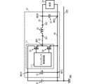
- FIG. 1 is a circuit diagram showing a schematic configuration of a switching power supply device according to a first embodiment of the present invention.
- FIG. 2 is an equivalent circuit diagram of the inductor according to the first embodiment of the present invention.
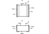
- FIG. 3A is a plan view of the inductor according to the first embodiment of the present invention, and
- FIG. 3B is a side view of the inductor.
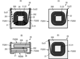
- FIG. 4(A) is a planar perspective view showing the configuration of a winding conductor of an inductor according to a first embodiment of the present invention
- FIG. 4(B) is a side perspective view showing the configuration of the winding conductor of this inductor
- FIGS. 4(C) and 4(D) are planar perspective views of each winding conductor.
- FIG. 4(A) is a planar perspective view showing the configuration of a winding conductor of an inductor according to a first embodiment of the present invention
- FIG. 4(B) is a side perspective view showing the configuration of the wind
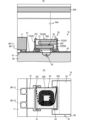
- FIG. 5A is a side cross-sectional view showing a configuration including a mounting portion of an inductor in a switching power supply device according to a first embodiment of the present invention
- FIG. 5B is a plan view of the mounting portion.
- FIG. 6 is a diagram illustrating a schematic flow of EMI noise in the switching power supply device according to the first embodiment of the present invention.
- FIG. 7 is a diagram illustrating the schematic flow of EMI noise in a switching power supply device of a comparative configuration.
- FIG. 8A is a graph showing the levels of conducted noise in the configuration of the present invention and the comparative configuration
- FIG. 8B is a graph showing the levels of radiated noise in the configuration of the present invention and the comparative configuration.
- FIG. 9 is a side cross-sectional view of a configuration including a mounting portion of an inductor in a switching power supply device according to a second embodiment of the present invention.
- FIG. 10 is a side cross-sectional view of a configuration including a mounting portion of an inductor in a switching power supply device according to a third embodiment of the present invention.
- FIG. 11 is a side cross-sectional view of a configuration including a mounting portion of an inductor in a switching power supply device according to a fourth embodiment of the present invention.
- FIG. 12 is a side perspective view showing the configuration of a winding conductor of an inductor according to a fifth embodiment of the present invention.
- FIG. 13 is a side perspective view showing the configuration of a winding conductor of an inductor according to a sixth embodiment of the present invention.
- 14A and 14B are planar perspective views showing each winding conductor of an inductor according to a seventh embodiment of the present invention.
- FIG. 15 is a side perspective view showing the configuration of a winding conductor of an inductor according to an eighth embodiment of the present invention.
- FIG. 16(A) is a side view showing the configuration of an inductor according to a ninth embodiment of the present invention
- FIG. 16(B) is a conceptual diagram showing the state in which a conductor pattern is wound around a magnetic core in this inductor.
- FIG. 17 is a circuit diagram showing a schematic configuration of a switching power supply device according to a tenth embodiment of the present invention.
- FIG. 1 is a circuit diagram showing a schematic configuration of a switching power supply device according to a first embodiment of the present invention.
- the switching power supply device 10 includes a switching IC 11, an inductor 20, an input capacitor 31, and an output capacitor 32.
- the switching IC 11 includes a switching control circuit 111, a switching element Q1, and a switching element Q2.
- the switching element Q1 corresponds to the "first switching element”
- the switching element Q2 corresponds to the "second switching element.”
- the switching elements Q1 and Q2 are power semiconductor elements and are formed, for example, by N-type MOS-FETs.
- the switching power supply device 10 is electrically connected to a DC power supply 81. More specifically, the input capacitor 31 is electrically connected in parallel to the DC power supply 81.
- the connection point between the positive electrode of the DC power supply 81 and the input capacitor 31 is node ND1H, and the connection point between the negative electrode of the DC power supply 81 and the input capacitor 31 is node ND1L.
- Switching element Q1 and switching element Q2 are electrically connected in series. More specifically, the source of switching element Q1 and the drain of switching element Q2 are electrically connected. The connection point between switching element Q1 and switching element Q2 is node ND0.
- Switching element Q1 and switching element Q2 are electrically connected to input capacitor 31. More specifically, the drain of switching element Q1 is connected to node ND1H on the Hi side of input capacitor 31. The source of switching element Q2 is connected to node ND1L on the Low side of input capacitor 31.
- switching element Q1 and the gate of switching element Q2 are electrically connected to a switching control circuit 111.
- Switching element Q1 and switching element Q2 electrically connect or disconnect the drain-source path according to a switching control signal from the switching control circuit 111.
- the inductor 20 has a first terminal 201 and a second terminal 202. Note that the specific electrical and physical configuration of the inductor 20 and the specific wiring pattern connected to the inductor 20 will be described later and will not be described here.
- the first terminal 201 of the inductor 20 is connected to the node ND0 of the switching IC 11 through the wiring pattern 41.
- the second terminal 202 of the inductor 20 is connected to one terminal (Hi side terminal) of the output capacitor 32 through the wiring pattern 42.
- the connection point between the second terminal 202 of the inductor 20 and one terminal of the output capacitor 32 is the node ND2H.
- the other terminal (low side terminal) of the output capacitor 32 is connected to the reference potential side wiring pattern 50.
- the connection point between the other terminal of the output capacitor 32 and the reference potential side wiring pattern 50 is node ND2L.
- the reference potential side wiring pattern 50 is connected to node ND1L (the connection point between the negative electrode of the DC power supply 81 and the input capacitor 31).
- the reference potential side wiring pattern 50 corresponds to the "reference potential pattern.”
- the switching power supply device 10 realizes a non-isolated step-down DC-DC converter (power conversion circuit).
- the load 82 is electrically connected in parallel to the output capacitor 32. More specifically, one terminal of the load 82 is connected to the node ND2H, and the other terminal of the load 82 is connected to the node ND2L.
- node ND1L of the switching power supply device 10 (the connection point between the negative electrode of the DC power supply 81 and the input capacitor 31) is electrically connected to a chassis CHS of a vehicle or the like on which the switching power supply device 10, the DC power supply 81, and the load 82 are mounted.
- the chassis CHS is connected to a ground potential as appropriate.
- the switching IC 11, inductor 20, input capacitor 31, and output capacitor 32 are realized by mounted electronic components. Furthermore, the wiring pattern that realizes the above-mentioned circuit configuration of the switching power supply device 10 is formed on a circuit board 60 (see FIG. 5(B) and the like described below). The switching power supply device 10 is realized by mounting the switching IC 11, inductor 20, input capacitor 31, and output capacitor 32 on the circuit board 60. This circuit board 60 is then physically and electrically connected to the chassis CHS.
- the inductor 20 includes a first winding 21, a second winding 22, a magnetic core 200, a first terminal 201, and a second terminal 202.
- the first winding 21 and the second winding 22 are connected in series between the first terminal 201 and the second terminal 202.
- the inductor 20 also has a parasitic capacitor 29 connected between the first terminal 201 and the second terminal 202.
- the inductor 20 has a parasitic capacitor 29 connected in parallel to the series circuit of the first winding 21 and the second winding 22.
- the capacitance of the parasitic capacitor 29 is determined by the structures of the first winding 21, the second winding 22, and the magnetic core 200.
- the parasitic capacitor 29 corresponds to the "internal parasitic capacitance of the inductor.”
- the inductor 20 has a resistance component due to the magnetic core 200 between the first terminal 201 and the second terminal 202.
- Fig. 3(A) is a plan view of the inductor according to the first embodiment of the present invention
- Fig. 3(B) is a side view of the inductor
- Fig. 4(A) is a plan perspective view showing the configuration of the winding conductor of the inductor according to the first embodiment of the present invention
- Fig. 4(B) is a side perspective view showing the configuration of the winding conductor of the inductor
- Figs. 4(C) and 4(D) are plan perspective views of each winding conductor.
- the inductor 20 comprises a first winding 21, a second winding 22, a magnetic core 200, a first terminal 201, and a second terminal 202.
- the magnetic core 200 is a substantially rectangular parallelepiped shape and has a top surface FU200, a bottom surface FB200, a side surface FS201, a side surface FS202, and two other side surfaces.
- Side surface FS201 and side surface FS202 face each other.
- the other two side surfaces face each other, are perpendicular to side surface FS201 and side surface FS202, and are connected to each other.
- Side surface FS201 corresponds to the "first side surface”
- side surface FS202 corresponds to the "second side surface”.
- the first winding 21 and the second winding 22 are winding conductors wound around a flat conductor.
- the first winding 21 is wound in a plan view and has a predetermined height.
- the height of the first winding 21 is greater than the thickness of the first winding 21 and the flat conductor in a plan view.
- the first winding 21 has a wound inner end Ei21 and an outer end Eo21.
- the second winding 22 has a configuration similar to that of the first winding 21.
- the second winding 22 has a wound inner end Ei22 and an outer end Eo22.
- the first winding 21 and the second winding 22 are built into the magnetic core 200 so that they are wound when viewed in a plane.
- the magnetic core 200 covers the first winding 21 and the second winding 22, and also fills the inside of the central opening of the winding shape of the first winding 21 and the second winding 22.
- the first winding 21 and the second winding 22 are stacked in the height direction of the magnetic core 200.
- the first winding 21 is arranged closer to the bottom surface FB200 than the second winding 22.
- the first winding 21 and the second winding 22 are arranged in this order from the bottom surface FB200 toward the top surface FU200 of the magnetic core 200.
- the first winding 21 and the second winding 22 are capacitively coupled to form a parasitic capacitor 29 (the internal parasitic capacitance of the inductor 20).
- This configuration also forms a resistance component due to the magnetic core 200.
- the inner end Ei21 of the first winding 21 and the inner end Ei22 of the second winding 22 are connected by a connecting conductor 28.
- the outer end Eo21 of the first winding 21 is exposed to the side surface FS201 of the magnetic core 200.
- the outer end Eo22 of the second winding 22 is exposed to the side surface FS202 of the magnetic core 200.
- a first terminal 201 made of a conductor is formed from the side surface FS201 to the bottom surface FB200 of the magnetic core 200. As a result, the outer end Eo21 of the first winding 21 is electrically connected to the first terminal 201.
- a second terminal 202 made of a conductor is formed from the side surface FS202 to the bottom surface FB200 of the magnetic core 200. As a result, the outer end Eo22 of the second winding 22 is electrically connected to the second terminal 202.
- the inductor 20 realizes the equivalent circuit configuration shown in Figure 2.
- FIG. 5(A) is a side cross-sectional view showing a configuration including an inductor mounting portion in a switching power supply device according to a first embodiment of the present invention
- Fig. 5(B) is a plan view of the mounting portion.
- Fig. 5(A) and Fig. 5(B) show a first winding 21 and a second winding 22 inside the inductor 20 so that the wiring inside the inductor 20 can be seen.
- the circuit symbol of a parasitic capacitor is also included for ease of explanation.
- the circuit board 60 comprises an insulating substrate and various conductor patterns formed on the insulating substrate.
- the circuit board 60 comprises a surface 61. Schematically, the switching IC 11, the inductor 20, the input capacitor 31, and the output capacitor 32 are mounted on the surface 61 of the circuit board 60.
- the various conductor patterns include the wiring pattern 41, the wiring pattern 42, and the reference potential side wiring pattern 50, and are formed on the circuit board 60 together with the switching IC 11, the inductor 20, the input capacitor 31, and the output capacitor 32 to realize the circuit configuration of the switching power supply device 10 shown in FIG. 1.
- the circuit board 60 is physically fixed to the chassis CHS by a fixing structure not shown.
- the ground potential of the circuit board 60 is electrically connected (grounded) to the chassis CHS by an electrical connection structure not shown.
- the specific structure of the mounting portion of the inductor 20 is as follows:
- wiring patterns 41 and 42 are formed on the surface 61 of the circuit board 60.
- a land on which the source terminal of the switching element Q1 of the switching IC 11 is mounted, and a land on which the drain terminal of the switching element Q2 of the switching IC 11 is mounted are formed.
- the source terminal of the switching element Q1 and the drain terminal of the switching element Q2 are mounted on the land by bumps BP111 and BP112, respectively. Therefore, one end of the wiring pattern 41 corresponds to the node ND0.
- a first land for the inductor is formed at the other end of the wiring pattern 41.
- the first terminal 201 of the inductor 20 is mounted on the first land for the inductor by solder or the like. As a result, the first terminal 201 of the inductor 20 is electrically and physically connected to the wiring pattern 41.
- One end of the wiring pattern 42 is spaced from the other end of the wiring pattern 41 by a distance according to the planar shape of the inductor 20.
- a second land for the inductor is formed at one end of the wiring pattern 42.
- the second terminal 202 of the inductor 20 is mounted on the second land for the inductor by solder or the like. As a result, the second terminal 202 of the inductor 20 is electrically and physically connected to the wiring pattern 42.
- one terminal (Hi side terminal) of the output capacitor 32 and one terminal of the load 82 are electrically and physically connected to predetermined positions of the wiring pattern 42.
- the inductor 20 is mounted on the circuit board 60 so that the spatial distance between the magnetic core 200 and the chassis CHS is long. More specifically, when the magnetic core 200 and the chassis CHS are arranged with a space between them, a parasitic capacitor Cpm is generated between the magnetic core 200 and the chassis CHS.
- the parasitic capacitor Cpm corresponds to the "external parasitic capacitance of the inductor.”
- the inductor 20 is mounted on the circuit board 60 at a position where the impedance Z29 due to the parasitic capacitor 29 (the internal parasitic capacitance of the inductor 20) is smaller than the impedance Zcpm due to the parasitic capacitor Cpm (the external parasitic capacitance of the inductor 20) at the switching frequency of the switching element Q1 and the switching element Q2.
- the inductor 20 is mounted on the circuit board 60 at a position where the relationship Z29 ⁇ Zcpm is satisfied.
- Z ⁇ Zcpm and furthermore, at the frequencies of the various harmonics of the switching frequency, it is preferable that Z29 ⁇ Zcpm and Z ⁇ Zcpm.
- the impedance Z29 due to such parasitic capacitor 29 and the impedance Zcpm due to parasitic capacitor Cpm can be measured by a device or system capable of measuring the impedance of an electrical circuit, such as an impedance analyzer or network analyzer.
- the switching power supply 10 forms an electrical closed circuit against switching noise (electromagnetic noise) as shown below, realizing a noise balancing circuit.
- FIG. 6 is a diagram showing the schematic flow of EMI noise in a switching power supply device according to the first embodiment of the present invention.
- the inductor 20 includes a parasitic capacitor 29, which is connected between the first terminal 201 and the second terminal 202.
- the impedance Z29 due to the parasitic capacitor 29 is smaller than the impedance Zcpm due to the parasitic capacitor Cpm (the external parasitic capacitance of the inductor 20).
- switching noise from node ND0 of switching IC 11 returns to switching IC 11 through wiring pattern 41, parasitic capacitor 29 of inductor 20, wiring pattern 42, output capacitor 32, reference potential side wiring pattern 50, input capacitor 31, and input side Hi potential pattern.
- the input side Hi potential pattern is a wiring pattern that connects the Hi side terminal of input capacitor 31 and the Hi side input terminal of switching IC 11 (the terminal connected to the drain terminal of switching element Q1).
- the propagation (leakage) of the switching noise from the magnetic core 200 of the inductor 20 to the chassis CHS is suppressed.
- the switching power supply device 10 has an electrical closed circuit for switching noise, which is made up of the switching IC 11, wiring pattern 41, parasitic capacitor 29 of the inductor 20, wiring pattern 42, output capacitor 32, reference potential side wiring pattern 50, input capacitor 31, and input side Hi potential pattern.
- the switching noise generated by the switching IC 11 is trapped by this closed electrical circuit. Furthermore, the switching noise radiated from the first winding 21 is guided to this closed electrical circuit by the second winding 22. And because the phase of the continuously generated switching noise is not constant, it is trapped in the closed electrical circuit and cancels out each other. In other words, this closed electrical circuit functions as a noise balancing circuit that balances the switching noise and suppresses the generation of common mode noise. In other words, the switching power supply 10 is equipped with a noise balancing circuit.
- the switching power supply device 10 can suppress the generation and conduction of common mode noise by suppressing the radiation or conduction of switching noise to the chassis CHS and the outside, and can suppress the level of switching noise by the noise balancing circuit. In other words, the switching power supply device 10 can more effectively suppress the radiation and conduction of switching noise and the generation and conduction of common mode noise. Furthermore, by suppressing the superposition of switching noise onto the chassis CHS and suppressing the generation of common mode noise caused by switching noise and its conduction at the chassis CHS, the switching power supply device 10 can suppress the adverse effects of switching noise on various electronic devices in a vehicle equipped with the chassis CHS.
- the switching power supply device 10 does not require separate components (shielding members) for suppressing the radiation and conduction of switching noise and for suppressing the generation and conduction of common mode noise, so a simple configuration and compact size can be achieved.
- FIG. 7 is a diagram that shows the schematic flow of EMI noise in a switching power supply device of a comparative configuration. If the configuration and mounting mode of the inductor 20 as in the switching power supply device 10 of the present application is not adopted, as shown in FIG. 7, the capacitance of the parasitic capacitor Cpm formed by the magnetic core 200 of the inductor 20 and the chassis CHS will be larger than the capacitance of the parasitic capacitor 29 of the inductor 20.
- parasitic capacitor Cpm (external parasitic capacitance of inductor 20) becomes more dominant than parasitic capacitor 29 (internal parasitic capacitance of inductor 20) in terms of switching noise transmission.
- parasitic capacitor Cpm external parasitic capacitance of inductor 20
- parasitic capacitor 29 internal parasitic capacitance of inductor 20
- the switching power supply device 10 of this embodiment can suppress the generation and conduction of common mode noise caused by switching noise coupling to the chassis CHS.
- FIG. 8(A) is a graph showing the levels of conducted noise in the present configuration and the comparative configuration
- FIG. 8(B) is a graph showing the levels of radiated noise in the present configuration and the comparative configuration. Note that FIG. 8(A) shows some frequency bands, but similar noise is distributed in wider frequency bands as well.
- the solid line shows the noise level of the present invention
- the dashed line shows the noise level of the comparative configuration. Furthermore, where the noise level of the present invention and the noise level of the comparative configuration overlap, the noise level of the present invention is illustrated as if it were overwriting the noise level of the comparative configuration.
- the conducted noise level in each frequency band can be suppressed to a low level.
- the radiated noise level in each frequency band can be suppressed to a low level.
- the radiated noise level in the 10 MHz band which is greater than 10 dBuV/m in the comparative configuration, can be suppressed to less than 10 dBuV/m.
- the inductor 20 has a laminated structure of a first winding 21 and a second winding 22.
- the first winding 21 and the second winding 22 are close to each other in the thickness direction of the magnetic core 200. This makes it easier for the inductor 20 to increase the capacitance of the parasitic capacitor 29. Therefore, by having the configuration of the inductor 20, the switching power supply device 10 can more reliably realize a noise balancing circuit consisting of the above-mentioned electric closed circuit against switching noise.
- the inductor 20 is mounted on the surface 61 of the circuit board 60 so that the bottom surface FB200 is closer to the surface 61 of the circuit board 60 than the top surface FU200, and so that the bottom surface FB200 faces the surface 61.
- the first winding 21 is disposed closer to the circuit board 60 than the second winding 22.
- the second winding 22 is disposed further outward than the first winding 21 in a direction perpendicular to the surface 61 of the circuit board 60.
- the first winding 21 is disposed between the second winding 22 and the surface 61 of the circuit board 60.
- One end of the wiring pattern 41 corresponds to node ND0 of switching element Q1 and switching element Q2. Therefore, noise caused by the switching operation of switching elements Q1 and Q2 flows through the wiring pattern 41.
- the wiring pattern 41 can be said to be a switching node pattern.
- the other end of the wiring pattern 41 is connected to the first winding 21. Therefore, switching noise flows into the first winding 21.
- one end of the second winding 22 is not directly connected to the node ND0 of the switching elements Q1 and Q2, but is connected to the node ND0 through the first winding 21. Furthermore, the other end of the second winding 22 is connected to the wiring pattern 42.
- the wiring pattern 42 is connected to the output capacitor 32, and has a stable potential. In other words, the wiring pattern 42 can be said to be a stable potential pattern.
- the second winding 22 connected to the stable potential pattern is disposed outside the first winding 21 connected to the switching node pattern, with the surface 61 of the circuit board 60 as the reference. Therefore, even if switching noise is radiated from the first winding 21, the second winding 22 prevents this switching noise from radiating outside the switching power supply device 10.
- the switching power supply device 10 has the following configuration.
- the area of the wiring pattern 41 is smaller than the area of the wiring pattern 42. In other words, the area of the switching node pattern is smaller than the area of the stable potential pattern. Therefore, the radiation of switching noise from the wiring pattern 41, which is the radiation source of the switching noise, to the outside of the switching power supply device 10 and to the chassis CHS is suppressed.
- the length is shortened without narrowing the width as much as possible. This reduces the resistance component of the wiring pattern 41. This allows the switching power supply device 10 to suppress losses due to current and achieve highly efficient power conversion. In particular, the switching power supply device 10 can achieve more efficient power conversion when a large current is required.
- the area of the wiring pattern 41 is smaller than the area of the inductor 20 projected onto the surface 61 of the circuit board 60 (the projected area of the inductor 20). This allows the switching power supply device 10 to suppress radiation and conduction of switching noise to the outside and to the chassis CHS, as well as the resulting generation and conduction of common mode noise.
- the area of the wiring pattern 42 is approximately the same as or larger than the projected area of the inductor 20. This makes the surface area of a relatively stable potential larger than the overall area of the switching power supply device 10 when viewed in a plan view. This makes it possible to suppress the effects of switching noise on the outside of the switching power supply device 10 and on the chassis CHS.
- the switching power supply 10 constitutes a step-down DC-DC converter, and the voltage (rectified and smoothed voltage) across the inductor 20 is lower than the voltage of the DC power supply 81. In such a case, the above-mentioned configuration is more effective. Furthermore, if, instead of the DC power supply 81, a commercial AC power supply is converted to DC via, for example, an inverter circuit and the input is received, the voltage across the inductor 20 (rectified and smoothed voltage) is lower than the commercial AC voltage. In this case as well, the above-mentioned configuration is more effective.
- Fig. 9 is a side cross-sectional view of a configuration including a mounting portion of an inductor in the switching power supply device according to the second embodiment of the present invention.
- the switching power supply device 10A according to the second embodiment differs from the switching power supply device 10 according to the first embodiment in the wiring pattern of the reference potential side wiring pattern 50.
- the other configuration of the switching power supply device 10A is the same as that of the switching power supply device 10, and a description of similar parts will be omitted.
- the switching power supply device 10A is formed by a circuit board 60A.
- the circuit board 60A has a reference potential side wiring pattern 50 made of a conductor pattern.
- the reference potential side wiring pattern 50 is formed inside the circuit board 60A. In plan view (viewed in a direction perpendicular to the surface 61), the reference potential side wiring pattern 50 overlaps the inductor 20 (the mounting area of the inductor 20) and the wiring pattern 41.
- a parasitic capacitor is formed between the inductor 20 and the wiring pattern 41, and the reference potential side wiring pattern 50. This parasitic capacitor does not carry the main current for power conversion, but rather allows switching noise with a higher frequency to flow.
- the internal parasitic capacitance that constitutes the electrical closed circuit can be made larger than the external parasitic capacitance with respect to the chassis CHS. This allows the switching noise to be more effectively confined to the noise balancing circuit, and the generation of common mode noise to be more effectively suppressed.
- the switching power supply device 10A can more effectively suppress external radiation and conduction of switching noise, as well as the generation and conduction of common mode noise.
- the reference potential side wiring pattern 50 only needs to overlap a portion of at least one of the inductor 20 and the wiring pattern 41, but it is preferable that it overlaps both the inductor 20 and the wiring pattern 41.
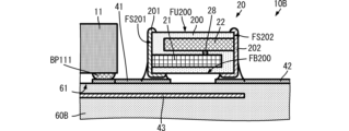
- FIG. 10 is a side cross-sectional view of a configuration including a mounting portion of an inductor in the switching power supply device according to the third embodiment of the present invention.
- the switching power supply device 10B according to the third embodiment differs from the switching power supply device 10 according to the first embodiment in the wiring pattern of the input side Hi potential pattern 43.
- the input side Hi potential pattern 43 corresponds to the "input wiring pattern.”
- the other configuration of the switching power supply device 10B is the same as that of the switching power supply device 10, and a description of similar parts will be omitted.
- the input side Hi potential pattern 43 is a wiring pattern that connects the node ND1H on the Hi potential side of the input capacitor 31 to the switching IC 11.
- the switching power supply device 10B is formed by a circuit board 60B.
- the circuit board 60B has an input side Hi potential pattern 43 made of a conductor pattern.
- the input side high potential pattern 43 is formed inside the circuit board 60B.
- the input side high potential pattern 43 overlaps the inductor 20 and the wiring pattern 41 in a plan view.
- a parasitic capacitor is formed between the inductor 20 and the wiring pattern 41 and the input side Hi potential pattern 43. This parasitic capacitor does not carry the main current for power conversion, but rather allows switching noise with a higher frequency to flow.
- the internal parasitic capacitance that constitutes the electrical closed circuit can be made larger than the external parasitic capacitance with respect to the chassis CHS. This allows the switching noise to be more effectively confined to the noise balancing circuit, and the generation of common mode noise to be more effectively suppressed.
- the switching power supply device 10B can more effectively suppress external radiation and conduction of switching noise, and the generation and conduction of common mode noise.
- the input side Hi potential pattern 43 only needs to overlap a portion of at least one of the inductor 20 and the wiring pattern 41, but it is preferable that it overlaps both the inductor 20 and the wiring pattern 41.
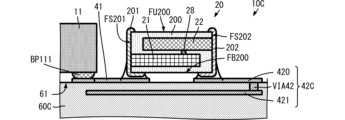
- FIG. 11 is a side cross-sectional view of a configuration including a mounting portion of an inductor in the switching power supply device according to the fourth embodiment of the present invention.
- the switching power supply device 10C according to the fourth embodiment differs from the switching power supply device 10 according to the first embodiment in the wiring pattern 42C.
- the other configuration of the switching power supply device 10C is the same as that of the switching power supply device 10, and a description of the similar parts will be omitted.
- the switching power supply device 10C is formed by a circuit board 60C.
- the circuit board 60C has a wiring pattern 42C made of a conductor pattern.
- the wiring pattern 42C includes a wiring pattern 420, a wiring pattern 421, and a connecting conductor VIA 42.
- the wiring pattern 420 is formed on the surface 61 of the circuit board 60C.
- the wiring pattern 420 includes a land for the inductor 20.
- the wiring pattern 421 is formed inside the circuit board 60C.
- the wiring pattern 421 is connected to the wiring pattern 420 through the connecting conductor VIA 42.
- the wiring pattern 421 overlaps the inductor 20 and the wiring pattern 41 in a planar view.
- a parasitic capacitor is formed between the inductor 20 and the wiring pattern 41, and the wiring pattern 421.
- This parasitic capacitor does not carry the main current for power conversion, but rather allows switching noise with a higher frequency to flow.
- the internal parasitic capacitance that constitutes the electrical closed circuit can be made larger than the external parasitic capacitance with respect to the chassis CHS. This allows the switching noise to be more effectively confined to the noise balancing circuit, and the generation of common mode noise to be more effectively suppressed.
- the switching power supply device 10C can more effectively suppress external radiation and conduction of switching noise, including common mode noise, and the generation and conduction of common mode noise.
- the wiring pattern 421 only needs to overlap a portion of at least one of the inductor 20 and the wiring pattern 41, but it is preferable that it overlaps both the inductor 20 and the wiring pattern 41.
- FIG. 12 is a side perspective view showing the configuration of a winding conductor of an inductor according to the fifth embodiment of the present invention.
- the switching power supply device according to the fifth embodiment differs from the switching power supply device 10 according to the first embodiment in the inductor 20D.
- the other configuration of the switching power supply device according to the fifth embodiment is similar to that of the switching power supply device 10, and a description of similar parts will be omitted.
- the inductor 20D has a first terminal 201D and a second terminal 202D.
- the first terminal 201D is formed across the side surface FS201 and the bottom surface FB200 of the magnetic core 200.
- the second terminal 202D is formed across the side surface FS202 and the bottom surface FB200 of the magnetic core 200.
- the height H201D of the first terminal 201D is smaller than the height H202D of the second terminal 202D.
- the first terminal 201D is formed across the entire width of the side surface FS201.
- the second terminal 202D is formed across the entire width of the side surface FS202.
- the area in which the first terminal 201D is formed on the side surface FS201 is smaller than the area in which the second terminal 202D is formed on the side surface FS202.
- This configuration suppresses the radiation of switching noise from the first terminal 201D.
- Fig. 13 is a side perspective view showing the configuration of a winding conductor of an inductor according to the sixth embodiment of the present invention.
- the switching power supply device according to the sixth embodiment differs from the switching power supply device 10 according to the first embodiment in the inductor 20E.
- the other configuration of the switching power supply device according to the sixth embodiment is similar to that of the switching power supply device 10, and a description of similar parts will be omitted.
- the inductor 20E has a first terminal 201E and a second terminal 202E.
- the first terminal 201E is formed on the bottom surface FB200 of the magnetic core 200, but not on the side surface FS201.
- the second terminal 202E is formed across the side surface FS202 and the bottom surface FB200 of the magnetic core 200.
- This configuration suppresses the radiation of switching noise from the first terminal 201E.
- FIGS. 14(A) and 14(B) are planar perspective views showing the winding conductors of an inductor according to the seventh embodiment of the present invention.
- the switching power supply device according to the seventh embodiment differs from the switching power supply device 10 according to the first embodiment in the inductor 20F.
- the other configuration of the switching power supply device according to the seventh embodiment is similar to that of the switching power supply device 10, and a description of similar parts will be omitted.
- the inductor 20F includes a first winding 21F and a second winding 22F.
- the number of turns of the second winding 22F is greater than the number of turns of the first winding 21F, and in a plan view, the area S22F of the outer shape of the second winding 22F is greater than the area S21F of the outer shape of the first winding 21F.
- the wound portion of the second winding 22F overlaps with the wound portion of the first winding 21F.
- the second winding 22F can more effectively suppress radiation of switching noise from the first winding 21F to the chassis CHS and the outside.
- FIG. 15 is a side perspective view showing the configuration of a winding conductor of an inductor according to the eighth embodiment of the present invention.
- the switching power supply device according to the eighth embodiment differs from the switching power supply device 10 according to the first embodiment in the inductor 20G.
- the other configuration of the switching power supply device according to the eighth embodiment is similar to that of the switching power supply device 10, and a description of similar parts will be omitted.
- the inductor 20G includes a first winding 21G, a second winding 22G, and a third winding 23G.
- the first winding 21G, the second winding 22G, and the third winding 23G are winding conductors, similar to the first winding 21 and the second winding 22 described above.
- the first winding 21G, the second winding 22G, and the third winding 23G are arranged in the following order from the bottom surface FB200 of the magnetic core 200 toward the top surface FU200: the first winding 21G, the third winding 23G, and the second winding 22G.
- the inner end Ei21 of the first winding 21G is connected to a portion (bottom surface portion) of the first terminal 201G formed on the bottom surface of the magnetic core 200 through the connecting conductor 281. More specifically, the inner end of the first winding 21G is connected to a position close to the center of the bottom surface portion of the first terminal 201G when viewed from above.
- the first terminal 201G may be formed only on the bottom surface of the magnetic core 200.
- the outer end Eo21 of the first winding 21G is connected to the outer end Eo23 of the third winding 23G through the connecting conductor 282.
- the inner end Ei23 of the third winding 23G is connected to the inner end Ei22 of the second winding 22G through the connecting conductor 283.
- the outer end Eo22 of the second winding 22G is connected to the second terminal 202G.
- the inductor used in the switching power supply device may be composed of three or more layers of winding conductors.
- the first winding 21G that is closest to the switching node pattern and first terminal 201G in terms of the electrical circuit is connected to the first terminal 201G and the switching node pattern through the inner end Ei21.
- the area with a high noise level is the center part when the inductor 20G is viewed in a plan view. Therefore, noise radiation from inductor 20G to chassis CHS and the outside is more effectively suppressed.
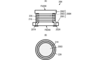
- FIG. 16(A) is a side view showing the configuration of an inductor according to the ninth embodiment of the present invention
- Fig. 16(B) is a conceptual diagram showing the state in which a conductor pattern is wound around a magnetic core in this inductor.
- the switching power supply device according to the ninth embodiment differs from the switching power supply device 10 according to the first embodiment in the inductor 20H.
- the other configuration of the switching power supply device according to the ninth embodiment is similar to that of the switching power supply device 10, and a description of similar parts will be omitted.
- the inductor 20H includes a magnetic core 200H, a fourth winding 21H, a fifth winding 22H, a first terminal 201H, and a second terminal 202H.
- the magnetic core 200H includes a bottom plate 2001, a top plate 2002, and a support pillar 2003.
- the support pillar 2003 is disposed between the bottom plate 2001 and the top plate 2002, and is connected to the bottom plate 2001 and the top plate 2002.
- the fourth winding 21H is a winding conductor wound around the support 2003. One end of the fourth winding 21H is connected to the first terminal 201H formed on the bottom plate 2001.
- the fifth winding 22H is a winding conductor wound around the support 2003 with the fourth winding 21H sandwiched between them. In other words, the fifth winding 22H is disposed outside the fourth winding 21H with the support 2003 as the reference. One end of the fifth winding 22H is connected to the other end of the fourth winding 21H. The other end of the fifth winding 22H is connected to the second terminal 202H formed on the bottom plate 2001.
- the first terminal 201H is connected to the wiring pattern 41, which is a switching node pattern.
- the second terminal 202H is connected to the wiring pattern 42, which is a stable potential pattern.
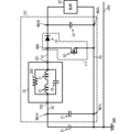
- FIG. 17 is a circuit diagram showing a schematic configuration of a switching power supply device according to the tenth embodiment of the present invention.
- the switching power supply 10 according to the first embodiment is a step-down DC-DC converter
- the switching power supply 10I according to the tenth embodiment is a step-up DC-DC converter.
- the configuration of the inductor 20 and the shapes of the wiring pattern 41 and wiring pattern 42 in the switching power supply 10I are the same as those in the switching power supply 10.
- the switching power supply device 10I includes a switching IC 11I, an inductor 20, an input capacitor 31, and an output capacitor 32.
- the switching IC 11I includes a switching control circuit (not shown), a switching element D1, and a switching element Q2.
- the switching element D1 corresponds to the "first switching element”
- the switching element Q2 corresponds to the "second switching element.”
- the switching elements D1 and Q2 are power semiconductor elements.
- the switching power supply device 10I is electrically connected to a DC power supply 81. More specifically, the input capacitor 31 is electrically connected in parallel to the DC power supply 81.
- the connection point between the positive electrode of the DC power supply 81 and the input capacitor 31 is node ND1H, and the connection point between the negative electrode of the DC power supply 81 and the input capacitor 31 is node ND1L.
- Switching element D1 and switching element Q2 are electrically connected in series. More specifically, the anode of switching element D1 and the drain of switching element Q2 are electrically connected. The connection point between switching element D1 and switching element Q2 is node ND0.
- a wiring pattern 42 is connected to the node ND1L.
- a second terminal 202 of the inductor 20 is connected to the wiring pattern 42.
- a first terminal 201 of the inductor 20 is connected to the wiring pattern 41, which is connected to the node ND0.
- One terminal (Hi side terminal) of the output capacitor 32 is connected to the cathode of the switching element D1.
- the connection point between the cathode of the switching element D1 and one terminal of the output capacitor 32 is the node ND2H.
- the other terminal (low side terminal) of the output capacitor 32 is connected to the reference potential side wiring pattern 50.
- the connection point between the other terminal of the output capacitor 32 and the reference potential side wiring pattern 50 is node ND2L.
- the reference potential side wiring pattern 50 is connected to node ND1L (the connection point between the negative electrode of the DC power supply 81 and the input capacitor 31).
- the switching power supply device 10I can realize a noise balancing circuit including the wiring pattern 41, the inductor 20, the wiring pattern 42, the input capacitor 31, the reference potential side wiring pattern 50, and the output capacitor 32.
- the switching power supply device 10I can suppress the external radiation of switching noise and the generation, conduction, and external radiation of common mode noise, and can suppress the noise level by the noise balancing circuit. Therefore, the switching power supply device 10I can more effectively suppress the radiation, conduction, and external radiation of switching noise to the chassis CHS, as well as the generation and conduction of common mode noise.
- the effect of suppressing common mode noise can be confirmed, for example, as follows.
- a delta-type LISN is connected to the wiring patterns on the positive and negative sides of the DC power supply 81, and a spectrum analyzer is connected to the delta-type LISN.
- the output voltage of the delta-type LISN is measured using the spectrum analyzer, allowing the common-mode noise suppression effect to be confirmed.
- a current sensor (current probe) is installed on the wiring pattern on the positive and negative sides of the DC power supply 81, and a spectrum analyzer is connected to the current sensor.
- the output current of the current sensor can be measured with the spectrum analyzer to confirm the effect of suppressing common mode noise.
- an LISN is connected to the wiring pattern on the negative side of the DC power supply 81, and this LISN is then connected to the chassis CHS.
- a current sensor current probe
- a spectrum analyzer is connected to the current sensor. The common mode noise suppression effect can be confirmed by measuring the output current of the current sensor with the spectrum analyzer.
- the winding conductor includes a first winding and a second winding arranged to be spaced apart from each other in a thickness direction of the magnetic core,
- the switching power supply device according to ⁇ 1>, wherein the internal parasitic capacitance is formed by the first winding and the second winding.
- the second winding is disposed at a position farther from the circuit board than the first winding,
- the switching power supply device of ⁇ 1> or ⁇ 2> wherein, in a plan view of the inductor, an outer shape of the second winding is smaller than an outer shape of the first winding, and the second winding overlaps the first winding.
- ⁇ 4> The inductor, at least one third winding electrically connected between the first winding and the first winding; an inner end of the first winding electrically connected to the first terminal;
- the switching power supply device according to any one of ⁇ 1> to ⁇ 3>, wherein an outer end of the second winding is electrically connected to the second terminal.
- ⁇ 5> A switching power supply device according to any one of ⁇ 1> to ⁇ 4>, wherein the reference potential pattern is formed in an area that overlaps the mounting area of the inductor when the circuit board is viewed in a plan view.
- the circuit board has an input wiring pattern electrically connected to the input capacitor,
- the switching power supply device according to any one of ⁇ 1> to ⁇ 5>, wherein the input wiring pattern is formed in an area overlapping a mounting area of the inductor in a plan view of the circuit board.
- a switching power supply device according to any one of ⁇ 1> to ⁇ 6>, in which a portion of the second wiring pattern is formed in an area that overlaps with the mounting area of the inductor when the circuit board is viewed in a plan view.
- the magnetic core has a bottom surface, a first side surface, and a second side surface, the first terminal is formed across the bottom surface and the first side surface, The second terminal is formed across the bottom surface and the second side surface,
- the switching power supply device according to any one of ⁇ 1> to ⁇ 7>, wherein an area of the first terminal formed on the first side surface is smaller than an area of the second terminal formed on the second side surface.
- the magnetic core has a bottom surface, a first side surface, and a second side surface, the first terminal is formed only on the bottom surface,
- the switching power supply device according to any one of ⁇ 1> to ⁇ 8>, wherein the second terminal is formed across the bottom surface and the second side surface.
- a switching power supply device according to any one of ⁇ 1> to ⁇ 9>, wherein the area of the first wiring pattern is smaller than the area of the inductor in a plan view.
- the first switching element, the second switching element, and the inductor configure a non-isolated power conversion circuit,
- the switching power supply device according to any one of ⁇ 1> to ⁇ 10>, wherein the rectified and smoothed voltage applied to the inductor is less than the rectified and smoothed voltage of a commercial AC voltage.
- An input capacitor an inductor including a winding conductor and a magnetic core, the inductor having a first terminal electrically connected to one end of the winding conductor and a second terminal electrically connected to the other end of the winding conductor; a first switching element and a second switching element electrically connected to the inductor;
Landscapes
- Engineering & Computer Science (AREA)
- Power Engineering (AREA)
- Microelectronics & Electronic Packaging (AREA)
- Physics & Mathematics (AREA)
- Electromagnetism (AREA)
- Dc-Dc Converters (AREA)
Priority Applications (3)
| Application Number | Priority Date | Filing Date | Title |
|---|---|---|---|
| DE112024000223.4T DE112024000223T5 (de) | 2023-03-13 | 2024-01-26 | Schaltnetzteil |
| JP2025506534A JP7878555B2 (ja) | 2023-03-13 | 2024-01-26 | スイッチング電源装置 |
| US19/311,059 US20250392212A1 (en) | 2023-03-13 | 2025-08-27 | Switching power supply |
Applications Claiming Priority (2)
| Application Number | Priority Date | Filing Date | Title |
|---|---|---|---|
| JP2023038590 | 2023-03-13 | ||
| JP2023-038590 | 2023-03-13 |
Related Child Applications (1)
| Application Number | Title | Priority Date | Filing Date |
|---|---|---|---|
| US19/311,059 Continuation US20250392212A1 (en) | 2023-03-13 | 2025-08-27 | Switching power supply |
Publications (1)
| Publication Number | Publication Date |
|---|---|
| WO2024190112A1 true WO2024190112A1 (ja) | 2024-09-19 |
Family
ID=92754549
Family Applications (1)
| Application Number | Title | Priority Date | Filing Date |
|---|---|---|---|
| PCT/JP2024/002401 Ceased WO2024190112A1 (ja) | 2023-03-13 | 2024-01-26 | スイッチング電源装置 |
Country Status (4)
| Country | Link |
|---|---|
| US (1) | US20250392212A1 (cg-RX-API-DMAC7.html) |
| JP (1) | JP7878555B2 (cg-RX-API-DMAC7.html) |
| DE (1) | DE112024000223T5 (cg-RX-API-DMAC7.html) |
| WO (1) | WO2024190112A1 (cg-RX-API-DMAC7.html) |
Citations (4)
| Publication number | Priority date | Publication date | Assignee | Title |
|---|---|---|---|---|
| JP2013099086A (ja) * | 2011-10-31 | 2013-05-20 | Cosel Co Ltd | スイッチング電源装置 |
| WO2017208420A1 (ja) * | 2016-06-02 | 2017-12-07 | 日産自動車株式会社 | 電力変換装置 |
| JP2019197836A (ja) * | 2018-05-10 | 2019-11-14 | 株式会社豊田中央研究所 | リアクトルおよびコンバータ回路 |
| JP2019220876A (ja) * | 2018-06-21 | 2019-12-26 | 株式会社デンソー | ブラシレスモータ制御装置 |
Family Cites Families (2)
| Publication number | Priority date | Publication date | Assignee | Title |
|---|---|---|---|---|
| JP6558354B2 (ja) * | 2016-12-09 | 2019-08-14 | 株式会社村田製作所 | シールド、電子回路、及び、dc−dcコンバータ |
| WO2023276797A1 (ja) | 2021-06-28 | 2023-01-05 | 株式会社村田製作所 | スイッチング電源装置 |
-
2024
- 2024-01-26 JP JP2025506534A patent/JP7878555B2/ja active Active
- 2024-01-26 DE DE112024000223.4T patent/DE112024000223T5/de active Pending
- 2024-01-26 WO PCT/JP2024/002401 patent/WO2024190112A1/ja not_active Ceased
-
2025
- 2025-08-27 US US19/311,059 patent/US20250392212A1/en active Pending
Patent Citations (4)
| Publication number | Priority date | Publication date | Assignee | Title |
|---|---|---|---|---|
| JP2013099086A (ja) * | 2011-10-31 | 2013-05-20 | Cosel Co Ltd | スイッチング電源装置 |
| WO2017208420A1 (ja) * | 2016-06-02 | 2017-12-07 | 日産自動車株式会社 | 電力変換装置 |
| JP2019197836A (ja) * | 2018-05-10 | 2019-11-14 | 株式会社豊田中央研究所 | リアクトルおよびコンバータ回路 |
| JP2019220876A (ja) * | 2018-06-21 | 2019-12-26 | 株式会社デンソー | ブラシレスモータ制御装置 |
Also Published As
| Publication number | Publication date |
|---|---|
| JP7878555B2 (ja) | 2026-06-23 |
| US20250392212A1 (en) | 2025-12-25 |
| JPWO2024190112A1 (cg-RX-API-DMAC7.html) | 2024-09-19 |
| DE112024000223T5 (de) | 2025-08-21 |
Similar Documents
| Publication | Publication Date | Title |
|---|---|---|
| CN103891116B (zh) | 电子装置 | |
| US5966294A (en) | Printed circuit board for prevention of unintentional electromagnetic interference | |
| JP5327289B2 (ja) | 電力変換装置 | |
| CN108235672B (zh) | 屏蔽体、电子电路以及dc-dc转换器 | |
| US20250392210A1 (en) | Switching power supply | |
| US12609615B2 (en) | Switching power supply device for reducing common mode noise generated by a switching element | |
| WO2010016367A1 (ja) | 複合電子部品 | |
| JP6935851B2 (ja) | 電力変換回路モジュール | |
| CN117253700A (zh) | 变压器 | |
| JP5951163B1 (ja) | ノイズフィルタ | |
| US20250096673A1 (en) | Switching power supply device | |
| US20250392212A1 (en) | Switching power supply | |
| KR101675401B1 (ko) | 전자파 장해 필터용 리액터 및 그것을 이용한 전자파 장해 필터 | |
| WO2024190018A1 (ja) | インダクタ部品およびスイッチング電源装置 | |
| JP7301120B1 (ja) | 電力変換装置 | |
| WO2026014107A1 (ja) | スイッチング電源装置 | |
| JP3823322B2 (ja) | 分布定数構造 | |
| JP3698206B2 (ja) | スイッチング電源装置 | |
| JP6699758B2 (ja) | モジュール部品 | |
| JP2024129404A (ja) | スイッチング電源装置 | |
| US20250096675A1 (en) | Switching power supply device | |
| JP7764950B2 (ja) | ノイズ低減機能部品を備えたスイッチング電源装置 | |
| JPWO2024190112A5 (cg-RX-API-DMAC7.html) | ||
| JP2001326439A (ja) | プリント回路の製造方法及び携帯通信機器 | |
| JP2024168986A (ja) | モータ制御装置 |
Legal Events
| Date | Code | Title | Description |
|---|---|---|---|
| 121 | Ep: the epo has been informed by wipo that ep was designated in this application |
Ref document number: 24770232 Country of ref document: EP Kind code of ref document: A1 |
|
| WWE | Wipo information: entry into national phase |
Ref document number: 2025506534 Country of ref document: JP |
|
| WWE | Wipo information: entry into national phase |
Ref document number: 112024000223 Country of ref document: DE |
|
| WWP | Wipo information: published in national office |
Ref document number: 112024000223 Country of ref document: DE |
|
| 122 | Ep: pct application non-entry in european phase |
Ref document number: 24770232 Country of ref document: EP Kind code of ref document: A1 |