WO2024181157A1 - 固体撮像素子 - Google Patents
固体撮像素子 Download PDFInfo
- Publication number
- WO2024181157A1 WO2024181157A1 PCT/JP2024/005330 JP2024005330W WO2024181157A1 WO 2024181157 A1 WO2024181157 A1 WO 2024181157A1 JP 2024005330 W JP2024005330 W JP 2024005330W WO 2024181157 A1 WO2024181157 A1 WO 2024181157A1
- Authority
- WO
- WIPO (PCT)
- Prior art keywords
- solid
- state imaging
- color filter
- blue
- imaging device
- Prior art date
- Legal status (The legal status is an assumption and is not a legal conclusion. Google has not performed a legal analysis and makes no representation as to the accuracy of the status listed.)
- Ceased
Links
Images


Classifications
-
- H—ELECTRICITY
- H10—SEMICONDUCTOR DEVICES; ELECTRIC SOLID-STATE DEVICES NOT OTHERWISE PROVIDED FOR
- H10F—INORGANIC SEMICONDUCTOR DEVICES SENSITIVE TO INFRARED RADIATION, LIGHT, ELECTROMAGNETIC RADIATION OF SHORTER WAVELENGTH OR CORPUSCULAR RADIATION
- H10F39/00—Integrated devices, or assemblies of multiple devices, comprising at least one element covered by group H10F30/00, e.g. radiation detectors comprising photodiode arrays
- H10F39/80—Constructional details of image sensors
- H10F39/806—Optical elements or arrangements associated with the image sensors
- H10F39/8063—Microlenses
-
- G—PHYSICS
- G02—OPTICS
- G02B—OPTICAL ELEMENTS, SYSTEMS OR APPARATUS
- G02B5/00—Optical elements other than lenses
- G02B5/20—Filters
-
- H—ELECTRICITY
- H10—SEMICONDUCTOR DEVICES; ELECTRIC SOLID-STATE DEVICES NOT OTHERWISE PROVIDED FOR
- H10F—INORGANIC SEMICONDUCTOR DEVICES SENSITIVE TO INFRARED RADIATION, LIGHT, ELECTROMAGNETIC RADIATION OF SHORTER WAVELENGTH OR CORPUSCULAR RADIATION
- H10F39/00—Integrated devices, or assemblies of multiple devices, comprising at least one element covered by group H10F30/00, e.g. radiation detectors comprising photodiode arrays
- H10F39/80—Constructional details of image sensors
- H10F39/805—Coatings
- H10F39/8053—Colour filters
-
- H—ELECTRICITY
- H10—SEMICONDUCTOR DEVICES; ELECTRIC SOLID-STATE DEVICES NOT OTHERWISE PROVIDED FOR
- H10F—INORGANIC SEMICONDUCTOR DEVICES SENSITIVE TO INFRARED RADIATION, LIGHT, ELECTROMAGNETIC RADIATION OF SHORTER WAVELENGTH OR CORPUSCULAR RADIATION
- H10F39/00—Integrated devices, or assemblies of multiple devices, comprising at least one element covered by group H10F30/00, e.g. radiation detectors comprising photodiode arrays
- H10F39/80—Constructional details of image sensors
- H10F39/805—Coatings
- H10F39/8057—Optical shielding
Definitions
- the present invention relates to solid-state imaging devices such as charge-coupled devices and complementary metal-oxide semiconductors.
- Digital still cameras and digital video cameras use solid-state imaging devices such as charge-coupled devices (CCDs) and complementary metal-oxide semiconductors (CMOSs) that use photoelectric conversion elements such as photodiodes.
- CCDs charge-coupled devices
- CMOSs complementary metal-oxide semiconductors
- incident light is collected by a microlens and sent to the photoelectric conversion element via a color filter.
- the microlenses are provided on the color filters, so if the refractive index of the color filters is greater than the refractive index of the microlenses, there is a risk that the efficiency of focusing light onto the photoelectric conversion element will decrease.
- the present invention aims to provide a solid-state imaging element that can prevent a decrease in the efficiency of light collection on the photoelectric conversion element.
- the solid-state imaging element of the present invention includes a semiconductor substrate having a plurality of photoelectric conversion elements, a microlens layer having a plurality of microlenses that respectively direct light to the photoelectric conversion elements of the semiconductor substrate, and a color filter disposed between the semiconductor substrate and the microlens layer, the color filter being characterized in that the transmittance of the color filter exhibits a maximum value between wavelengths of 400 nm and 500 nm and exhibits 50% between wavelengths of 460 nm and 490 nm, and the refractive index is smaller than that of the microlens at the wavelength where the transmittance exhibits the maximum value.
- the color filter in the above-mentioned solid-state imaging device contains a blue pigment and a blue-violet dye.
- the color filter further contains a blue-violet pigment in the above-mentioned solid-state imaging device.
- the ratio of the blue-violet pigment to the blue-violet dye in the color filter is 0.1 or more and 10 or less.
- the ratio of the total amount of the blue-violet dye and the blue-violet pigment to the blue pigment in the color filter is 0.1 or more and 1 or less.
- the color filter contains the blue pigment, the blue-violet dye, and the blue-violet pigment in a range of 30% by mass or more and 70% by mass or less with respect to the total mass of the solid contents.
- the refractive index of the color filter in the above-mentioned solid-state imaging device is 1.5 or more and less than 1.6 at the wavelength of the transmittance at the maximum value.
- the thickness of the color filter in the above-mentioned solid-state imaging device is 0.3 ⁇ m or more and 1.0 ⁇ m or less.
- the refractive index of the microlens is 1.60 or more and 1.65 or less within the wavelength range of 400 nm or more and 500 nm or less.
- the height of the microlenses is 0.3 ⁇ m or more and 1.0 ⁇ m or less.
- the transmittance of the color filter is maximum between wavelengths of 400 nm and 500 nm, and is 50% between wavelengths of 460 nm and 490 nm.
- the refractive index of the color filter is smaller than that of the microlens at the wavelengths where the transmittance is maximum. This prevents a decrease in the efficiency of focusing blue light from the microlens to the photoelectric conversion element, improving the light focusing performance and improving the peak sensitivity between wavelengths of 400 nm and 500 nm.
- 1 is a cross-sectional view illustrating a schematic structure of a main part of a main embodiment of a solid-state imaging device according to the present invention.
- 1 is a graph showing the relationship between wavelength and transmittance of a test sample and a comparative sample color filter.
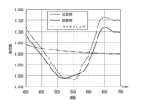
- 1 is a graph showing the relationship between wavelength and refractive index of a color filter and a microlens of a test sample and a comparative sample.
- photoelectric conversion elements 12 such as photodiodes that convert light into electrical signals
- Such semiconductor substrates 11 usually have a protective layer (not shown) on the top surface for the purpose of protecting and flattening the surface (light incident surface).
- the semiconductor substrate 11 is made of a material that transmits visible light and can withstand temperatures of about 300° C.
- materials include Si, oxides such as SiO2 , nitrides such as SiN, mixtures of these, and materials containing Si.
- a light-shielding layer 13 is disposed on the semiconductor substrate 11, blocking a portion of the incident light corresponding to the light-receiving region of the photoelectric conversion element 12.
- a plurality of color filters 14A-14C of different colors are disposed on the light-shielding layer 13 so as to correspond to each photoelectric conversion element 12.
- the color filters 14A-14C are arranged in a predetermined pattern, and correspond to the colors that separate the incident light.
- color filters 14A-14C are arranged in a Bayer array, which is a regular pattern that is preset to correspond to each of the multiple photoelectric conversion elements 12 according to the pixel position. Note that the color filters 14A-14C are not necessarily limited to a Bayer array, and other arrays are also possible.
- partitions 15 are disposed between adjacent color filters 14A-14C. It is also possible to omit the partitions 15.
- a microlens layer 16 is disposed on the color filters 14A-14C.
- the microlens layer 16 has a plurality of protruding hemispherical microlenses 17 that allow light to enter the color filters 14A-14C in correspondence with each photoelectric conversion element 12. In other words, the color filters 14A-14C are disposed between the semiconductor substrate 11 and the microlens layer 16.
- the refractive index of the microlens 17 is between 1.60 and 1.65 inclusive within the wavelength range of 400 nm to 500 nm.
- An example of a material for the microlens 17 with such a refractive index is "TMR P15 (product number)" manufactured by Tokyo Ohka Kogyo Co., Ltd.
- the microlens 17 can also contain a hollow silica filler or other filler.
- the height (T1) of the microlens 17, which is the shortest distance between its bottom and top, is preferably 0.3 ⁇ m or more and 1.0 ⁇ m or less, and more preferably 0.4 ⁇ m or more and 0.7 ⁇ m or less. If it is less than 0.3 ⁇ m, the light-gathering ability decreases, which is undesirable, and if it exceeds 1.0 ⁇ m, patterning by photolithography becomes difficult, which is undesirable.
- the color filters 14A-14C are made of a colorless and transparent resin material to which a colorant of a specific color and various additives have been added.
- resin materials for the color filters 14A-14C include acrylic resin and epoxy resin.
- the color filter 14A is mixed with a green pigment (GP) such as C.I. Pigment Green 7, 10, 36, 37, or 58 as a coloring material, or a zinc phthalocyanine pigment as described in JP-A-2008-19383, JP-A-2007-320986, or JP-A-2004-70342, or an aluminum phthalocyanine pigment as described in JP-A-4893859, etc.
- GP green pigment
- the color filter 14B contains, as a coloring material, for example, C.I. Pigment Red 7, 14, 41, 48:1, 48:2, 48:3, 48:4, 57:1, 81, 81:1, 81:2, 81:3, 81:4, 122, 146, 149, 166, 168, 169, 176, 177, 178, 179, 184, 185, 187, 200, 202, 208, 210, 221, 224, 242, 246, 254, 255, 26 4,268,269,270,272,273,274,276,277,278,279,280,281,282,283,284,285,286,287, diketopyrrolopyrrole pigments described in JP-T-2011-523433, and naphthol azo pigments described in JP-A-2013-161025 are mixed with red pigments (RP).
- RP red pigments
- the color filter 14C contains, as coloring materials, blue pigments (BP) such as C.I. Pigment Blue 1, 1:2, 9, 14, 15, 15:1, 15:2, 15:3, 15:4, 15:6, 16, 22, 60, 64 and copper phthalocyanine pigments described in JP-A-2004-333817 and JP-A-4893859, C.I. Acid Red 50, 51, 52, 87, 91, 92, 94, 289, 388, C.I. Acid Violet 9, 30, 102, C.I. Basic Red 1 (Rhodamine 6G), 2, 3, 4, 8, 10, 11, C.I. Basic Violet 10 (Rhodamine B), 11, C.I. At least a blue-violet dye (VD) such as Solvent Red 218, C.I.
- BP blue pigments
- Mordant Red 27, C.I. Reactive Red 36 (Rose Bengal B), Sulforhodamine G, or a xanthene dye or cyanine dye described in JP-A-2010-32999 and JP-A-4492760 is mixed with the color filter 14C. It is preferable that the color filter 14C further contains a blue-violet pigment (VP) such as a dioxazine pigment such as C.I. Pigment Violet 1, 19, 23, 29, 32, 36, or 38.
- VP blue-violet pigment
- the above-mentioned additives include sensitizers, antioxidants, dissolved oxygen reducers, leveling agents, storage stabilizers, adhesion improvers, dispersion aids, etc.
- the green pigment (GP) is contained in the range of 30% by mass to 65% by mass, and more preferably in the range of 50% by mass to 65% by mass, based on the mass of the total solid content (TS). If it is less than 50% by mass, it is difficult to fully exert the function as a color filter, which is undesirable, and if it exceeds 65% by mass, it is undesirable that the photosensitive component is easily insufficient, making it difficult to form a pattern.
- the red pigment (RP) is preferably contained in the range of 30% by mass to 65% by mass, and more preferably in the range of 50% by mass to 65% by mass, relative to the mass of the total solid content (TS). If it is less than 50% by mass, it is difficult to fully exert the function as a color filter, which is undesirable, and if it exceeds 65% by mass, the photosensitive component tends to be insufficient, making it difficult to form a pattern, which is undesirable.
- the ratio (VP/VD) of the blue-violet pigment (VP) to the blue-violet dye (VD) is preferably 0.1 or more and 10 or less, and more preferably 0.1 or more and 1 or less. If it is less than 0.1, the light resistance is likely to decrease, which is undesirable, and if it exceeds 10, the color characteristics are likely to decrease, which is undesirable.
- the ratio (VDP/BP) of the total amount (VDP) of the blue-violet dye (VD) and blue-violet pigment (VP) to the blue pigment (BP) is preferably 0.1 or more and 1 or less, and more preferably 0.1 or more and 0.5 or less. If it is less than 0.1, crosstalk with Green tends to increase and color reproducibility tends to decrease, which is undesirable, and if it exceeds 1, floating tends to occur on the long wavelength side of the spectrum and color purity tends to decrease, which is undesirable.
- the blue pigment (BP), the blue-violet dye (VD), and the blue-violet pigment (VP) are preferably contained in the range of 30% by mass to 70% by mass, and more preferably in the range of 45% by mass to 55% by mass, relative to the mass of the total solid content (TS). If it is less than 30% by mass, it becomes difficult to fully exhibit the function as a color filter, which is undesirable, and if it exceeds 70% by mass, it leads to a decrease in light transmittance, which is undesirable.
- the color filter 14C has a maximum transmittance within a wavelength range of 400 nm to 500 nm, i.e., the maximum transmittance is between 400 nm and 500 nm (see FIG. 2).
- the color filter 14C has a transmittance of 50% within a wavelength range of 460 nm to 490 nm, i.e., the maximum transmittance is between 460 nm and 490 nm (see FIG. 2).
- the color filter 14C also has a refractive index that is smaller than that of the microlens 17 (1.5 or more and less than 1.6) at the wavelength where the transmittance is at the maximum (see FIG. 3).
- the color filters 14A-14C preferably have a thickness T2 in the light transmission direction of 0.3 ⁇ m or more and 1.0 ⁇ m or less, and more preferably 0.4 ⁇ m or more and 0.7 ⁇ m or less. If it is less than 0.3 ⁇ m, it is difficult to fully exert the function as a color filter, which is undesirable, and if it exceeds 1.0 ⁇ m, it is difficult for light to reach the bottom of the film during exposure due to absorption by the coloring material, which is undesirable as it is likely to cause a decrease in patterning properties.
- the solid-state imaging element 10 according to the present embodiment described above can be manufactured by applying a known method. That is, a light-shielding layer 13 is provided on a semiconductor substrate 11 on which photoelectric conversion elements 12 are provided, color filters 14A-14C and partition walls 15 are provided on the light-shielding layer 13, and then a microlens layer 16 is further provided, and microlenses 17 are formed in the microlens layer 16 by etching or the like.
- the solid-state imaging element 10 when light ⁇ enters the microlens 17, the light ⁇ is collected by the microlens 17, color-separated by the color filters 14A-14C, and sent to each photoelectric conversion element 12 via the light-shielding layer 13.
- the transmittance of color filter 14C has a maximum value in the wavelength range of 400 nm to 500 nm and is 50% in the wavelength range of 460 nm to 490 nm, and the refractive index is a value (1.5 or more and less than 1.6) smaller than that of microlens 17 (1.60 or more and 1.65 or less) at the wavelength of the transmittance at the maximum value. Therefore, it is possible to prevent a decrease in the efficiency of focusing blue light from microlens 17 to photoelectric conversion element 12, and to improve the focusing performance.
- the solid-state imaging element 10 can prevent a decrease in light collection efficiency and improve light collection performance, thereby improving peak sensitivity in the wavelength range of 400 nm or more and 500 nm or less.
- substituents that contribute to the refractive index of the resin material that constitutes the microlens or color filter generally, firstly, there are those containing a benzene ring, -SC 6 H 5 > -COC 6 H 5 > -OC 6 H 5 > -C 6 H 5 , followed by -NH 2 > -NO 2 > -OH > -CN > -OCH 3 and heavy halogens (-I) > -Br > -Cl, etc.
- pyridine structures and alkyl groups do not change the refractive index very much, while -F has the effect of significantly reducing the refractive index due to its small polarizability.
- test specimen of the solid-state imaging element 10 shown in FIG. 1 and described in the above embodiment was prepared under the following conditions, and a conventional comparison specimen for comparison was also prepared under the following conditions.
- Micro Lens 17 Resin material: phenolic resin Height: 0.5 ⁇ m Refractive index: see Figure 3
- the transmittance of both the test and comparison color filters is maximum at a wavelength of 450 nm.
- the refractive index of the comparison color filter at a wavelength of 450 nm (1.625) is equal to the refractive index of the microlens.
- the refractive index of the test color filter (1.59) is smaller than the refractive index of the microlens (1.625).
- the peak sensitivity at a wavelength of 450 nm was 3.2% higher for the test specimen than for the comparative specimen. This is greater than the difference (2.1%) between the transmittance at a wavelength of 450 nm of the above color filter of the test specimen (83.7%) and the transmittance at a wavelength of 450 nm of the above color filter of the comparative specimen (81.6%), and is therefore considered to be due to the improved light collection efficiency and improved light collection performance.
- Example 1-10 color filters were created as in Example 1-10, with the above VP/VD, VDP/BP, and BVPD/TS values changed, and the peak transmittance was determined.
- the peak transmittance difference which is the difference from the transmittance (81.6%) of the above comparative color filter at a wavelength of 450 nm, was then calculated (the value obtained by subtracting the comparative body value from each value of Example 1-10). The results are shown in Table 1 below.
- the solid-state imaging device can improve peak sensitivity in the wavelength range from 400 nm to 500 nm, making it highly effective for use in a variety of industries.
Landscapes
- Physics & Mathematics (AREA)
- General Physics & Mathematics (AREA)
- Optics & Photonics (AREA)
- Solid State Image Pick-Up Elements (AREA)
- Optical Filters (AREA)
- Transforming Light Signals Into Electric Signals (AREA)
Priority Applications (4)
| Application Number | Priority Date | Filing Date | Title |
|---|---|---|---|
| JP2025503770A JPWO2024181157A1 (https=) | 2023-03-02 | 2024-02-15 | |
| CN202480015819.7A CN120814355A (zh) | 2023-03-02 | 2024-02-15 | 固体拍摄元件 |
| EP24763640.0A EP4675685A1 (en) | 2023-03-02 | 2024-02-15 | Solid-state imaging element |
| US19/316,330 US20260006931A1 (en) | 2023-03-02 | 2025-09-02 | Solid-state imaging element having a plurality of microlenses |
Applications Claiming Priority (2)
| Application Number | Priority Date | Filing Date | Title |
|---|---|---|---|
| JP2023-032130 | 2023-03-02 | ||
| JP2023032130 | 2023-03-02 |
Related Child Applications (1)
| Application Number | Title | Priority Date | Filing Date |
|---|---|---|---|
| US19/316,330 Continuation US20260006931A1 (en) | 2023-03-02 | 2025-09-02 | Solid-state imaging element having a plurality of microlenses |
Publications (1)
| Publication Number | Publication Date |
|---|---|
| WO2024181157A1 true WO2024181157A1 (ja) | 2024-09-06 |
Family
ID=92589784
Family Applications (1)
| Application Number | Title | Priority Date | Filing Date |
|---|---|---|---|
| PCT/JP2024/005330 Ceased WO2024181157A1 (ja) | 2023-03-02 | 2024-02-15 | 固体撮像素子 |
Country Status (6)
| Country | Link |
|---|---|
| US (1) | US20260006931A1 (https=) |
| EP (1) | EP4675685A1 (https=) |
| JP (1) | JPWO2024181157A1 (https=) |
| CN (1) | CN120814355A (https=) |
| TW (1) | TW202507340A (https=) |
| WO (1) | WO2024181157A1 (https=) |
Citations (14)
| Publication number | Priority date | Publication date | Assignee | Title |
|---|---|---|---|---|
| JP2004070342A (ja) | 2002-07-24 | 2004-03-04 | Dainippon Printing Co Ltd | カラーフィルター用緑色顔料、緑色顔料分散体、感光性着色組成物、カラーフィルター、及び、液晶パネル |
| JP2004333817A (ja) | 2003-05-07 | 2004-11-25 | Fujifilm Arch Co Ltd | Lcd用硬化性緑色組成物およびカラーフィルタ |
| JP2004335598A (ja) * | 2003-05-02 | 2004-11-25 | Toppan Printing Co Ltd | 固体撮像素子及びその製造方法 |
| WO2006134740A1 (ja) * | 2005-06-17 | 2006-12-21 | Toppan Printing Co., Ltd. | 撮像素子 |
| JP2007320986A (ja) | 2006-05-30 | 2007-12-13 | Dainippon Ink & Chem Inc | ポリハロゲン化亜鉛フタロシアニン顔料組成物及びカラーフィルタ |
| JP2008019383A (ja) | 2006-07-14 | 2008-01-31 | Dainippon Ink & Chem Inc | ポリハロゲン化亜鉛フタロシアニン、感光性組成物およびカラーフィルター |
| JP2010032999A (ja) | 2008-07-01 | 2010-02-12 | Sumitomo Chemical Co Ltd | 着色感光性樹脂組成物 |
| JP4492760B1 (ja) | 2009-12-01 | 2010-06-30 | 東洋インキ製造株式会社 | カラーフィルタ用青色着色組成物、およびカラーフィルタ |
| US20100237247A1 (en) * | 2009-03-18 | 2010-09-23 | Hui-Hsuan Chen | IR sensing device |
| JP2011523433A (ja) | 2008-05-28 | 2011-08-11 | ビーエーエスエフ ソシエタス・ヨーロピア | 改良された赤色フィルター組成物 |
| JP4893859B1 (ja) | 2011-01-28 | 2012-03-07 | 東洋インキScホールディングス株式会社 | カラーフィルタ用着色組成物、およびカラーフィルタ |
| JP2013015817A (ja) | 2011-06-06 | 2013-01-24 | Fujifilm Corp | カラーフィルタ、ccdセンサ、cmosセンサ、有機cmosセンサ、および固体撮像素子 |
| JP2013161025A (ja) | 2012-02-08 | 2013-08-19 | Yazaki Corp | ヘッドアップディスプレイ装置 |
| JP2019056758A (ja) * | 2017-09-20 | 2019-04-11 | Agc株式会社 | 光学装置および光学部材 |
-
2024
- 2024-02-15 JP JP2025503770A patent/JPWO2024181157A1/ja active Pending
- 2024-02-15 EP EP24763640.0A patent/EP4675685A1/en active Pending
- 2024-02-15 CN CN202480015819.7A patent/CN120814355A/zh active Pending
- 2024-02-15 WO PCT/JP2024/005330 patent/WO2024181157A1/ja not_active Ceased
- 2024-03-01 TW TW113107410A patent/TW202507340A/zh unknown
-
2025
- 2025-09-02 US US19/316,330 patent/US20260006931A1/en active Pending
Patent Citations (14)
| Publication number | Priority date | Publication date | Assignee | Title |
|---|---|---|---|---|
| JP2004070342A (ja) | 2002-07-24 | 2004-03-04 | Dainippon Printing Co Ltd | カラーフィルター用緑色顔料、緑色顔料分散体、感光性着色組成物、カラーフィルター、及び、液晶パネル |
| JP2004335598A (ja) * | 2003-05-02 | 2004-11-25 | Toppan Printing Co Ltd | 固体撮像素子及びその製造方法 |
| JP2004333817A (ja) | 2003-05-07 | 2004-11-25 | Fujifilm Arch Co Ltd | Lcd用硬化性緑色組成物およびカラーフィルタ |
| WO2006134740A1 (ja) * | 2005-06-17 | 2006-12-21 | Toppan Printing Co., Ltd. | 撮像素子 |
| JP2007320986A (ja) | 2006-05-30 | 2007-12-13 | Dainippon Ink & Chem Inc | ポリハロゲン化亜鉛フタロシアニン顔料組成物及びカラーフィルタ |
| JP2008019383A (ja) | 2006-07-14 | 2008-01-31 | Dainippon Ink & Chem Inc | ポリハロゲン化亜鉛フタロシアニン、感光性組成物およびカラーフィルター |
| JP2011523433A (ja) | 2008-05-28 | 2011-08-11 | ビーエーエスエフ ソシエタス・ヨーロピア | 改良された赤色フィルター組成物 |
| JP2010032999A (ja) | 2008-07-01 | 2010-02-12 | Sumitomo Chemical Co Ltd | 着色感光性樹脂組成物 |
| US20100237247A1 (en) * | 2009-03-18 | 2010-09-23 | Hui-Hsuan Chen | IR sensing device |
| JP4492760B1 (ja) | 2009-12-01 | 2010-06-30 | 東洋インキ製造株式会社 | カラーフィルタ用青色着色組成物、およびカラーフィルタ |
| JP4893859B1 (ja) | 2011-01-28 | 2012-03-07 | 東洋インキScホールディングス株式会社 | カラーフィルタ用着色組成物、およびカラーフィルタ |
| JP2013015817A (ja) | 2011-06-06 | 2013-01-24 | Fujifilm Corp | カラーフィルタ、ccdセンサ、cmosセンサ、有機cmosセンサ、および固体撮像素子 |
| JP2013161025A (ja) | 2012-02-08 | 2013-08-19 | Yazaki Corp | ヘッドアップディスプレイ装置 |
| JP2019056758A (ja) * | 2017-09-20 | 2019-04-11 | Agc株式会社 | 光学装置および光学部材 |
Non-Patent Citations (1)
| Title |
|---|
| See also references of EP4675685A1 |
Also Published As
| Publication number | Publication date |
|---|---|
| TW202507340A (zh) | 2025-02-16 |
| EP4675685A1 (en) | 2026-01-07 |
| CN120814355A (zh) | 2025-10-17 |
| US20260006931A1 (en) | 2026-01-01 |
| JPWO2024181157A1 (https=) | 2024-09-06 |
Similar Documents
| Publication | Publication Date | Title |
|---|---|---|
| KR101852804B1 (ko) | 적외선 센서, 근적외선 흡수 조성물, 감광성 수지 조성물, 화합물, 근적외선 흡수 필터 및 촬상 장치 | |
| KR102261468B1 (ko) | 구조체, 근적외선 투과 필터층 형성용 조성물 및 광센서 | |
| TWI819187B (zh) | 固態攝影元件用濾光片、及固態攝影元件 | |
| US20070187794A1 (en) | Imaging device | |
| JP2009111225A (ja) | 固体撮像素子及びその製造方法 | |
| KR20210039503A (ko) | 착색 감광성 조성물, 경화막, 컬러 필터, 차광막, 고체 촬상 소자, 화상 표시 장치, 및 경화막의 제조 방법 | |
| AU2003248253A1 (en) | Solid-state imaging device and production method therefor | |
| JP2004200360A (ja) | 固体撮像素子及びその製造方法 | |
| US12237352B2 (en) | Solid-state imaging element having partition wall disposed between optical filters | |
| KR20200031054A (ko) | 촬상 장치, 및 적외 흡수막 | |
| JP2023029378A (ja) | 構造体、固体撮像素子および画像表示装置 | |
| US8395699B2 (en) | Solid-state imaging device, camera, electronic apparatus, and method for manufacturing solid-state imaging device | |
| JP2000180621A (ja) | オンチップカラーフィルタ及びこれを用いた固体撮像素子 | |
| US20050045805A1 (en) | Solid-state image sensor and a manufacturing method thereof | |
| WO2024181157A1 (ja) | 固体撮像素子 | |
| JP7615570B2 (ja) | 固体撮像素子 | |
| JP2000294758A (ja) | 固体撮像素子 | |
| JP2003222719A (ja) | 有機顔料を用いたカラーフィルタ | |
| JP2010078680A (ja) | カラーフィルタ及び固体撮像素子 | |
| KR20240107130A (ko) | 구조체 및 고체 촬상 소자 | |
| US20050186489A1 (en) | Color filter materials, color filters, manufacturing method and image sensor | |
| JP2024137208A (ja) | カラーフィルタ及び固体撮像素子 | |
| JP2024036168A (ja) | カラーフィルタ及び固体撮像素子 | |
| JP2005093659A (ja) | 固体撮像素子 | |
| JP2023119416A (ja) | 赤外光パスフィルター、着色組成物、固体撮像素子用フィルター、および、固体撮像素子 |
Legal Events
| Date | Code | Title | Description |
|---|---|---|---|
| 121 | Ep: the epo has been informed by wipo that ep was designated in this application |
Ref document number: 24763640 Country of ref document: EP Kind code of ref document: A1 |
|
| WWE | Wipo information: entry into national phase |
Ref document number: 2025503770 Country of ref document: JP |
|
| WWE | Wipo information: entry into national phase |
Ref document number: 202480015819.7 Country of ref document: CN |
|
| WWE | Wipo information: entry into national phase |
Ref document number: 2024763640 Country of ref document: EP |
|
| NENP | Non-entry into the national phase |
Ref country code: DE |
|
| WWP | Wipo information: published in national office |
Ref document number: 202480015819.7 Country of ref document: CN |
|
| ENP | Entry into the national phase |
Ref document number: 2024763640 Country of ref document: EP Effective date: 20251002 |
|
| ENP | Entry into the national phase |
Ref document number: 2024763640 Country of ref document: EP Effective date: 20251002 |
|
| ENP | Entry into the national phase |
Ref document number: 2024763640 Country of ref document: EP Effective date: 20251002 |
|
| WWP | Wipo information: published in national office |
Ref document number: 2024763640 Country of ref document: EP |