WO2024176989A1 - 半導体装置 - Google Patents
半導体装置 Download PDFInfo
- Publication number
- WO2024176989A1 WO2024176989A1 PCT/JP2024/005656 JP2024005656W WO2024176989A1 WO 2024176989 A1 WO2024176989 A1 WO 2024176989A1 JP 2024005656 W JP2024005656 W JP 2024005656W WO 2024176989 A1 WO2024176989 A1 WO 2024176989A1
- Authority
- WO
- WIPO (PCT)
- Prior art keywords
- resin
- semiconductor device
- external connection
- connection terminal
- electrically connected
- Prior art date
- Legal status (The legal status is an assumption and is not a legal conclusion. Google has not performed a legal analysis and makes no representation as to the accuracy of the status listed.)
- Ceased
Links
Images


Classifications
-
- H—ELECTRICITY
- H10—SEMICONDUCTOR DEVICES; ELECTRIC SOLID-STATE DEVICES NOT OTHERWISE PROVIDED FOR
- H10W—GENERIC PACKAGES, INTERCONNECTIONS, CONNECTORS OR OTHER CONSTRUCTIONAL DETAILS OF DEVICES COVERED BY CLASS H10
- H10W72/00—Interconnections or connectors in packages
- H10W72/50—Bond wires
-
- H—ELECTRICITY
- H10—SEMICONDUCTOR DEVICES; ELECTRIC SOLID-STATE DEVICES NOT OTHERWISE PROVIDED FOR
- H10W—GENERIC PACKAGES, INTERCONNECTIONS, CONNECTORS OR OTHER CONSTRUCTIONAL DETAILS OF DEVICES COVERED BY CLASS H10
- H10W20/00—Interconnections in chips, wafers or substrates
- H10W20/40—Interconnections external to wafers or substrates, e.g. back-end-of-line [BEOL] metallisations or vias connecting to gate electrodes
- H10W20/41—Interconnections external to wafers or substrates, e.g. back-end-of-line [BEOL] metallisations or vias connecting to gate electrodes characterised by their conductive parts
- H10W20/435—Cross-sectional shapes or dispositions of interconnections
-
- H—ELECTRICITY
- H10—SEMICONDUCTOR DEVICES; ELECTRIC SOLID-STATE DEVICES NOT OTHERWISE PROVIDED FOR
- H10W—GENERIC PACKAGES, INTERCONNECTIONS, CONNECTORS OR OTHER CONSTRUCTIONAL DETAILS OF DEVICES COVERED BY CLASS H10
- H10W70/00—Package substrates; Interposers; Redistribution layers [RDL]
- H10W70/60—Insulating or insulated package substrates; Interposers; Redistribution layers
- H10W70/611—Insulating or insulated package substrates; Interposers; Redistribution layers for connecting multiple chips together
- H10W70/614—Insulating or insulated package substrates; Interposers; Redistribution layers for connecting multiple chips together the multiple chips being integrally enclosed
-
- H—ELECTRICITY
- H10—SEMICONDUCTOR DEVICES; ELECTRIC SOLID-STATE DEVICES NOT OTHERWISE PROVIDED FOR
- H10W—GENERIC PACKAGES, INTERCONNECTIONS, CONNECTORS OR OTHER CONSTRUCTIONAL DETAILS OF DEVICES COVERED BY CLASS H10
- H10W70/00—Package substrates; Interposers; Redistribution layers [RDL]
- H10W70/60—Insulating or insulated package substrates; Interposers; Redistribution layers
- H10W70/62—Insulating or insulated package substrates; Interposers; Redistribution layers characterised by their interconnections
- H10W70/65—Shapes or dispositions of interconnections
-
- H—ELECTRICITY
- H10—SEMICONDUCTOR DEVICES; ELECTRIC SOLID-STATE DEVICES NOT OTHERWISE PROVIDED FOR
- H10W—GENERIC PACKAGES, INTERCONNECTIONS, CONNECTORS OR OTHER CONSTRUCTIONAL DETAILS OF DEVICES COVERED BY CLASS H10
- H10W74/00—Encapsulations, e.g. protective coatings
- H10W74/10—Encapsulations, e.g. protective coatings characterised by their shape or disposition
- H10W74/111—Encapsulations, e.g. protective coatings characterised by their shape or disposition the semiconductor body being completely enclosed
- H10W74/114—Encapsulations, e.g. protective coatings characterised by their shape or disposition the semiconductor body being completely enclosed by a substrate and the encapsulations
-
- H—ELECTRICITY
- H10—SEMICONDUCTOR DEVICES; ELECTRIC SOLID-STATE DEVICES NOT OTHERWISE PROVIDED FOR
- H10W—GENERIC PACKAGES, INTERCONNECTIONS, CONNECTORS OR OTHER CONSTRUCTIONAL DETAILS OF DEVICES COVERED BY CLASS H10
- H10W90/00—Package configurations
-
- H—ELECTRICITY
- H10—SEMICONDUCTOR DEVICES; ELECTRIC SOLID-STATE DEVICES NOT OTHERWISE PROVIDED FOR
- H10W—GENERIC PACKAGES, INTERCONNECTIONS, CONNECTORS OR OTHER CONSTRUCTIONAL DETAILS OF DEVICES COVERED BY CLASS H10
- H10W72/00—Interconnections or connectors in packages
- H10W72/30—Die-attach connectors
-
- H—ELECTRICITY
- H10—SEMICONDUCTOR DEVICES; ELECTRIC SOLID-STATE DEVICES NOT OTHERWISE PROVIDED FOR
- H10W—GENERIC PACKAGES, INTERCONNECTIONS, CONNECTORS OR OTHER CONSTRUCTIONAL DETAILS OF DEVICES COVERED BY CLASS H10
- H10W72/00—Interconnections or connectors in packages
- H10W72/851—Dispositions of multiple connectors or interconnections
- H10W72/853—On the same surface
- H10W72/865—Die-attach connectors and bond wires
-
- H—ELECTRICITY
- H10—SEMICONDUCTOR DEVICES; ELECTRIC SOLID-STATE DEVICES NOT OTHERWISE PROVIDED FOR
- H10W—GENERIC PACKAGES, INTERCONNECTIONS, CONNECTORS OR OTHER CONSTRUCTIONAL DETAILS OF DEVICES COVERED BY CLASS H10
- H10W90/00—Package configurations
- H10W90/701—Package configurations characterised by the relative positions of pads or connectors relative to package parts
- H10W90/731—Package configurations characterised by the relative positions of pads or connectors relative to package parts of die-attach connectors
- H10W90/736—Package configurations characterised by the relative positions of pads or connectors relative to package parts of die-attach connectors between a chip and a stacked lead frame, conducting package substrate or heat sink
-
- H—ELECTRICITY
- H10—SEMICONDUCTOR DEVICES; ELECTRIC SOLID-STATE DEVICES NOT OTHERWISE PROVIDED FOR
- H10W—GENERIC PACKAGES, INTERCONNECTIONS, CONNECTORS OR OTHER CONSTRUCTIONAL DETAILS OF DEVICES COVERED BY CLASS H10
- H10W90/00—Package configurations
- H10W90/701—Package configurations characterised by the relative positions of pads or connectors relative to package parts
- H10W90/751—Package configurations characterised by the relative positions of pads or connectors relative to package parts of bond wires
- H10W90/756—Package configurations characterised by the relative positions of pads or connectors relative to package parts of bond wires between a chip and a stacked lead frame, conducting package substrate or heat sink
Definitions
- This disclosure relates to a semiconductor device.
- semiconductor devices include a transformer used to transmit signals and power.
- the transformer includes a pair of coils arranged opposite each other in the vertical direction (see, for example, Patent Document 1).
- a semiconductor device includes a semiconductor element including an element front surface and an element back surface facing opposite each other in the thickness direction, an element insulating layer including an insulating surface constituting the element front surface, and a first conductor provided within the element insulating layer, a second conductor arranged at a distance from the first conductor in the thickness direction, and a sealing resin in contact with the element insulating layer and sealing the semiconductor element and the second conductor, the first conductor and the second conductor facing each other in the thickness direction with the element insulating layer and the sealing resin in between.
- the semiconductor device according to one aspect of the present disclosure can improve the dielectric strength voltage.
- FIG. 1 is a circuit diagram showing a schematic configuration of a signal transmission device including a semiconductor device according to a first embodiment.
- FIG. 2 is a perspective view showing a schematic diagram of the signal transmission device of FIG.
- FIG. 3 is a schematic perspective view showing the semiconductor device of FIG.
- FIG. 4 is a schematic perspective view of the semiconductor device of FIG. 3 as viewed from a different direction.
- FIG. 5 is a schematic plan view showing the configuration of the semiconductor device of FIG.
- FIG. 6 is a schematic plan view showing the configuration of a semiconductor element included in the semiconductor device of FIG.
- FIG. 7 is a schematic plan view showing a configuration related to the second coil of the semiconductor device of FIG.
- FIG. 8 is a schematic cross-sectional view taken along line 8-8 in FIG.
- FIG. 1 is a circuit diagram showing a schematic configuration of a signal transmission device including a semiconductor device according to a first embodiment.
- FIG. 2 is a perspective view showing a schematic diagram of the signal transmission device of FIG.
- FIG. 9 is a schematic cross-sectional view taken along line 9-9 in FIG.
- FIG. 10 is a schematic perspective view showing a semiconductor device according to a modified example.
- FIG. 11 is a schematic perspective view of the semiconductor device of FIG. 10 as viewed from a different direction.
- FIG. 12 is a schematic cross-sectional view of the semiconductor device of FIG.
- FIG. 13 is a schematic perspective view showing a semiconductor device according to the second embodiment.
- FIG. 14 is a schematic perspective view of the semiconductor device of FIG. 13 as viewed from a different direction.
- FIG. 15 is a schematic plan view showing the configuration of the semiconductor device of FIG.
- FIG. 16 is a schematic plan view showing a configuration related to the second coil of the semiconductor device of FIG. FIG.
- FIG. 17 is a schematic cross-sectional view taken along line 17-17 in FIG.
- FIG. 18 is a schematic cross-sectional view taken along line 18-18 in FIG.
- FIG. 19 is a schematic perspective view showing a semiconductor device according to a modified example.
- FIG. 20 is a schematic perspective view of the semiconductor device of FIG. 19 viewed from a different direction.
- 21 is a schematic bottom view of the semiconductor device of FIG.
- FIG. 22 is a schematic cross-sectional view of the semiconductor device of FIG.
- FIG. 23 is a schematic perspective view showing a semiconductor device according to the third embodiment.
- FIG. 24 is a schematic perspective view of the semiconductor device of FIG. 23 viewed from a different direction.
- FIG. 25 is a schematic plan view showing the configuration of the semiconductor device of FIG. FIG.
- FIG. 26 is a schematic plan view showing a configuration related to the second coil of the semiconductor device of FIG. 23.
- FIG. 27 is a schematic cross-sectional view taken along line 27-27 in FIG.
- FIG. 28 is a schematic cross-sectional view taken along line 28-28 in FIG.
- FIG. 29 is a schematic bottom view showing a semiconductor device according to a modified example.
- FIG. 30 is a schematic cross-sectional view of the semiconductor device of FIG.
- FIG. 31 is a schematic plan view showing a semiconductor device according to a modified example.
- FIG. 32 is a schematic cross-sectional view of FIG.
- FIG. 33 is a schematic plan view showing a semiconductor device according to a modified example.
- FIG. 34 is a schematic cross-sectional view of the semiconductor device of FIG.
- At least one means “one or more” of the desired options.
- at least one means “only one option” or “both of two options” if the number of options is two.
- at least one means “only one option” or “any combination of two or more options” if the number of options is three or more.
- Figure 1 shows a simplified example of the circuit configuration of the signal transmission device 900.
- Figure 2 is a perspective view showing the signal transmission device 900.
- the signal transmission device 900 is a device that transmits a pulse signal while electrically isolating a first terminal 901 and a second terminal 902.
- the signal transmission device 900 is, for example, a digital isolator.
- the signal transmission device 900 includes a first circuit 911 electrically connected to the first terminal 901, a second circuit 912 electrically connected to the second terminal 902, and a transformer 913 that electrically isolates the first circuit 911 and the second circuit 912.
- the first circuit 911 is a circuit configured to operate when a first voltage V1 is applied.
- the first circuit 911 is electrically connected to, for example, an external control device (not shown).
- the first circuit 911 includes a transmission circuit 911A.
- the second circuit 912 is a circuit configured to operate when a second voltage V2 different from the first voltage V1 is applied.
- the second voltage V2 is, for example, higher than the first voltage V1.
- the first voltage V1 and the second voltage V2 are DC voltages.
- the second circuit 912 is electrically connected to, for example, a drive circuit that is controlled by the control device.
- An example of a drive circuit is a switching circuit.
- the second circuit 912 includes a reception circuit 912A.
- the ground of the first circuit 911 and the ground of the second circuit 912 are provided independently of each other.
- the transformer 913 is connected between the transmitting circuit 911A and the receiving circuit 912A.
- the transformer 913 includes two coils 913A and 913B.
- the coil 913A is connected to the transmitting circuit 911A, and the coil 913B is connected to the receiving circuit 912A.
- a control signal from a control device is input to the transmitting circuit 911A of the first circuit 911 through the first terminal 901.
- the control signal passes from the transmitting circuit 911A of the first circuit 911 through the transformer 913 and is received by the receiving circuit 912A of the second circuit 912.
- the signal transmitted to the second circuit 912 is output from the second circuit 912 to the drive circuit through the second terminal 902.
- the first terminal 901 can be considered an input terminal that inputs a signal to the signal transmission device 900.
- the second terminal 902 can be considered an output terminal from which a signal is output from the signal transmission device 900.
- the first circuit 911 and the second circuit 912 are electrically insulated by the transformer 913. More specifically, the transformer 913 regulates the transmission of DC voltage between the first circuit 911 and the second circuit 912. Furthermore, the transformer 913 allows the transmission of pulse signals between the first circuit 911 and the second circuit 912.
- the state in which the first circuit 911 and the second circuit 912 are insulated means a state in which the transmission of DC voltage between the first circuit 911 and the second circuit 912 is blocked, while the transmission of a pulse signal from the first circuit 911 to the second circuit 912 is permitted.
- the second circuit 912 is configured to receive a signal from the first circuit 911.
- the signal transmission device 900 includes a substrate 920 and a plurality of semiconductor devices 931 , 932 , and 10 .
- the substrate 920 is formed, for example, in a quadrangular plate shape.
- the substrate 920 includes a substrate front surface 921 and a substrate back surface 922 facing the opposite side to the substrate front surface 921.
- the substrate front surface 921 and the substrate back surface 922 are, for example, rectangular in shape.
- a plurality of first terminals 941 and a plurality of second terminals 942 are formed on the substrate surface 921.
- the plurality of first terminals 941 and the plurality of second terminals 942 are formed of a material containing, for example, Cu (copper).
- the plurality of first terminals 941 are disposed at a first end 923 of the substrate 920.
- the plurality of second terminals 942 are disposed at a second end 924 of the substrate 920 opposite the first end 923.
- the multiple first terminals 941 include a power supply terminal that supplies the first voltage V1 shown in FIG. 1, a ground terminal that is connected to the ground of the first circuit 911, and the first terminal 901.
- the multiple second terminals 942 include a power supply terminal that supplies the second voltage V2 shown in FIG. 1, a ground terminal that is connected to the ground of the second circuit 912, and the second terminal 902.
- the semiconductor devices 931, 932, and 10 are mounted on a substrate surface 921 of the substrate 920.
- the semiconductor devices 931, 932, and 10 are connected to pads (not shown) formed on the substrate surface 921.
- the pads are connected to a first terminal 941 and a second terminal 942 by wiring (not shown).
- the substrate 920 may be, for example, a semiconductor substrate, an insulating substrate formed from a material containing epoxy resin or the like, an insulating substrate formed from a material containing glass, an insulating substrate formed from a material containing ceramics such as alumina, or the like.
- Semiconductor device 931 includes a first circuit 911 shown in FIG. 1.
- Semiconductor device 932 includes a second circuit 912 shown in FIG. 1.
- Semiconductor device 10 includes a transformer 913 shown in FIG. 1.
- Semiconductor devices 931, 932, and 10 can be referred to as semiconductor chips.
- Signal transmission device 900 can be referred to as a semiconductor module.
- Signal transmission device 900 can also be referred to as a multi-chip module including multiple semiconductor chips.
- the semiconductor device 10 including the transformer 913 can be said to be an insulating chip that provides insulation between the semiconductor device 931 including the first circuit 911 and the semiconductor device 932 including the second circuit 912.
- the semiconductor devices 931, 932, and 10 are arranged in the order of the semiconductor device 931 including the first circuit 911, the semiconductor device 10 including the transformer 913, and the semiconductor device 932 including the second circuit 912 from the first terminal 941 to the second terminal 942.
- the signal transmission device 900 may include a sealing member that seals the multiple semiconductor devices 931, 932, and 10 mounted on the substrate surface 921.
- the sealing member may be, for example, a case that houses the substrate 920 and the multiple semiconductor devices 931, 932, and 10.
- the case may be filled with a resin such as silicone resin.
- the sealing member may be a sealing resin that covers at least the multiple semiconductor devices 931, 932, and 10.
- the sealing resin may be, for example, a molded resin containing epoxy resin or the like.
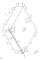
- FIGS. 3 and 4 are perspective views showing the appearance of the semiconductor device 10, where FIG. 3 is a perspective view of the semiconductor device 10 seen from the top side, and FIG. 4 is a perspective view of the semiconductor device 10 seen from the bottom side.
- FIG. 5 is a plan view of the semiconductor device 10 seen from the bottom side. Note that FIG. 5 shows the sealing resin 80 and the element insulating layer 22 in a see-through manner.
- FIG. 6 is a plan view showing the semiconductor element 20. Note that FIG. 6 shows the element insulating layer 22 in a see-through manner.
- FIG. 7 is a plan view showing the conductive part 40. Note that FIG.
- FIG. 7 shows the sealing resin 80 in a see-through manner. Note that FIG. 7 shows the outline of the semiconductor element 20 by a dashed line.
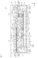
- FIG. 8 is a schematic cross-sectional view of the semiconductor device 10 cut along line 8-8 in FIG. 5.
- FIG. 9 is a schematic cross-sectional view of the semiconductor device 10 cut along line 9-9 in FIG. Note that, for convenience, in FIGS. 8 and 9, members that are not on the line showing the cross-sectional position may be shown, or the positions and sizes of members may differ from those in FIGS. 5 to 7.
- the semiconductor device 10 is, for example, a rectangular parallelepiped.
- the thickness direction of the semiconductor device 10 is defined as the z direction.
- the direction perpendicular to the z direction is defined as the x direction, and the direction perpendicular to the z direction and the x direction is defined as the y direction. Viewing an object from the z direction is referred to as viewing it in a planar view.
- the semiconductor device 10 includes a device top surface 10S, a device bottom surface 10R, and multiple device side surfaces 11, 12, 13, and 14.
- the device top surface 10S and the device bottom surface 10R face in opposite directions from each other in the z direction.
- the multiple device side surfaces 11, 12, 13, and 14 intersect the device top surface 10S and the device bottom surface 10R.
- the device side surfaces 11 and 12 face in opposite directions from each other in the x direction.
- the device side surfaces 13 and 14 face in opposite directions from each other in the y direction.
- the semiconductor device 10 includes a semiconductor element 20, a conductive portion 40, a joint portion SD, and a sealing resin 80.
- the semiconductor element 20 includes a first coil 26.
- the conductive portion 40 includes a second coil 43 and external connection terminals 51A, 51B, 61A, and 61B.
- the first coil 26 and the second coil 43 correspond to the coils 913A and 913B shown in FIG. 1.
- the semiconductor element 20 is mounted on the conductive portion 40, and the first coil 26 of the semiconductor element 20 faces the second coil 43 of the conductive portion 40 in the z direction.
- the external connection terminals 51A, 51B, 61A, and 61B are exposed from the resin bottom surface 80R of the sealing resin 80.
- the semiconductor device 10 is mounted on the substrate 920 shown in FIG. 2 by the external connection terminals 51A, 51B, 61A, and 61B.
- the semiconductor element 20 includes an element front surface 20S, an element rear surface 20R, and element side surfaces 201, 202, 203, and 204.
- the element front surface 20S and the element rear surface 20R face in opposite directions in the z direction.
- the element front surface 20S faces the same direction as the resin lower surface 80R.
- the semiconductor element 20 is arranged so that the element front surface 20S faces in the same direction as the resin lower surface.
- the element side surfaces 201, 202, 203, and 204 intersect with the element front surface 20S and the element rear surface 20R.
- the element side surfaces 201, 202, 203, and 204 are perpendicular to the element front surface 20S and the element rear surface 20R.
- the element side surfaces 201 and 202 face in opposite directions in the x direction.
- the element side surfaces 203 and 204 face in opposite directions in the y direction.
- the semiconductor element 20 includes an element substrate 21.
- the element substrate 21 is a semiconductor substrate, and is formed of a material that includes, for example, silicon (Si).
- the element substrate 21 is a Si substrate.
- the element substrate 21 has a substrate main surface 21S, a substrate back surface 21R, and multiple substrate side surfaces 211, 212, 213, and 214.
- the substrate main surface 21S and the substrate back surface 21R face opposite each other in the Z direction.
- the substrate side surfaces 211 and 212 face opposite each other in the X direction.
- the substrate side surfaces 213 and 214 face opposite each other in the Y direction.
- the substrate main surface 21S faces the element connection portions 53A and 53B, dummy element connection portions 53C and 53D, and second coil 43 of the conductive portion 40.
- the substrate back surface 21R faces the same direction as the resin top surface 80S.
- the element insulating layer 22 is formed to cover the substrate main surface 21S.
- the element insulating layer 22 includes an insulating front surface 22S, an insulating back surface 22R, and multiple insulating side surfaces 221, 222, 223, and 224.
- the insulating front surface 22S of the element insulating layer 22 faces the same direction as the substrate main surface 21S.
- the insulating back surface 22R of the element insulating layer 22 faces the opposite side to the insulating front surface 22S of the element insulating layer 22.
- the insulating back surface 22R of the element insulating layer 22 faces the substrate main surface 21S side and contacts the substrate main surface 21S.
- Each of the insulating side surfaces 221, 222, 223, and 224 of the element insulating layer 22 faces the same direction as each of the element side surfaces 201, 202, 203, and 204.
- the insulating front surface 22S of the element insulating layer 22 constitutes the element front surface 20S of the semiconductor element 20.
- the substrate rear surface 21R of the element substrate 21 constitutes the element rear surface 20R of the semiconductor element 20.
- the substrate side surfaces 211-214 of the element substrate 21 and the insulating side surfaces 221-224 of the element insulating layer 22 constitute the element side surfaces 201-204 of the semiconductor element 20.
- the semiconductor element 20 includes a first coil 26.
- the first coil 26 corresponds to a "first conductor.”
- the first coil 26 is formed in a spiral shape in a plan view.
- the first coil 26 includes an outer first end 26A and an inner second end 26B.
- the first end 26A corresponds to an "outer end.”
- the second end 26B corresponds to an "inner end.”
- the first coil 26 is provided in the element insulating layer 22.
- the element insulating layer 22 includes three insulating layers 23, 24, and 25.
- the insulating layers 23, 24, and 25 are stacked in this order from the substrate main surface 21S of the element substrate 21.
- the first coil 26 is formed on the surface 24S of the second insulating layer 24.
- the first coil 26 and the surface 24S of the second insulating layer 24 are covered by the third insulating layer 25.
- the element insulating layer 22 has insulating properties.
- the first insulating layer 23 and the second insulating layer 24 are made of a material containing, for example, Si (silicon).
- the first insulating layer 23 and the second insulating layer 24 are made of, for example, SiO 2 (silicon oxide), SiN (silicon nitride), or the like.
- the third insulating layer 25 is made of a resin having insulating properties, such as polyimide resin, phenolic resin, or epoxy resin.
- the third insulating layer 25 may be made of a material containing, for example, Si.
- the semiconductor element 20 includes a plurality of connection pads 27A, 27B, 27C, and 27D.
- the plurality of connection pads 27A to 27D are arranged in the same position as the first coil 26 in the z direction.
- the plurality of connection pads 27A to 27D are provided on the surface 24S of the second insulating layer 24.
- the third insulating layer 25 is formed so as to cover the periphery of the connection pads 27A to 27D.
- the third insulating layer 25 includes an opening 25X that exposes a portion of the connection pads 27A to 27D.
- connection pad 27A is electrically connected to first end 26A of first coil 26.
- Connection pad 27B is electrically connected to second end 26B of first coil 26 by element wiring 28.
- first coil 26 is connected between connection pad 27A and connection pad 27B.
- first coil 26 is not electrically connected to connection pad 27C and connection pad 27D. Connection pads 27C and 27D that are not electrically connected to first coil 26 in this manner correspond to "dummy connection pads.”
- the element wiring 28 is formed on the surface 23S of the first insulating layer 23.
- the element wiring 28 is formed of a material including, for example, Cu, Al (aluminum), etc.
- a first end 28A of the element wiring 28 is electrically connected to the first coil 26 by a via 29A.
- a second end 28B of the element wiring 28 is electrically connected to the connection pad 27B by a via 29B.
- the vias 29A and 29B penetrate the second insulating layer 24.
- the vias 29A and 29B are formed of a material including, for example, Cu, Al, W (tungsten), etc.
- the semiconductor element 20 includes element electrodes 31A, 31B, 31C, and 31D electrically connected to a plurality of connection pads 27A, 27B, 27C, and 27D.
- the element electrodes 31A, 31B, 31C, and 31D are electrically connected to the connection pads 27A, 27B, 27C, and 27D, respectively, by connection wiring 30.
- the element electrodes 31A to 31D are arranged so as to overlap the connection pads 27A to 27D in a plan view.
- connection pads 27A, 27B are electrically connected to the first coil 26. Therefore, element electrodes 31A, 31B electrically connected to connection pads 27A, 27B are electrically connected to the first coil 26. On the other hand, connection pads 27C, 27D are not electrically connected to the first coil 26. Therefore, element electrodes 31C, 31D electrically connected to connection pads 27C, 27D are not electrically connected to the first coil 26. In this way, element electrodes 31C, 31D that are not electrically connected to the first coil 26 correspond to "dummy element electrodes.”
- the element electrodes 31A to 31D include a conductive layer 32 and a barrier layer 33.
- the conductive layer 32 is made of a material containing Cu, for example.
- the conductive layer 32 may be made of multiple metal layers.
- the conductive layer 32 may include a seed layer.
- the seed layer is made of, for example, Ti (titanium)/Cu.
- the barrier layer 33 is made of a material containing Ni.
- the barrier layer 33 may be made of multiple metal layers.
- the barrier layer 33 is made of, for example, Ni (nickel), Pd (palladium), Au (gold), an alloy containing two or more of these metals, etc.
- the conductive portion 40 includes a first wiring member 41 , a second wiring member 42 , and a second coil 43 .
- the first wiring member 41 includes a first external connection terminal 51A, a second external connection terminal 51B, a first element connection portion 53A, a second element connection portion 53B, a first connection wiring 54A, and a second connection wiring 54B.
- the second wiring member 42 includes a third external connection terminal 61A, a fourth external connection terminal 61B, and a third connection wiring 64.
- the third connection wiring 64 corresponds to the "second lead-out wiring.”
- the first external connection terminal 51A, the second external connection terminal 51B, the third external connection terminal 61A, and the fourth external connection terminal 61B are formed in a rectangular shape in a plan view.
- the shapes of the first external connection terminal 51A, the second external connection terminal 51B, the third external connection terminal 61A, and the fourth external connection terminal 61B can be changed to any shape, such as a circle or a polygon, in a plan view.
- the first external connection terminal 51A, the second external connection terminal 51B, the third external connection terminal 61A, and the fourth external connection terminal 61B are exposed from the resin bottom surface 80R of the sealing resin 80.
- the first external connection terminal 51A and the second external connection terminal 51B are arranged along the device side surface 12 of the semiconductor device 10, in one example.
- the first external connection terminal 51A and the second external connection terminal 51B are arranged at a distance in the y direction.
- the first external connection terminal 51A and the second external connection terminal 51B are arranged side by side in the y direction in a plan view.
- the first external connection terminal 51A is arranged at a corner portion formed by the device side surface 12 and the device side surface 13 of the semiconductor device 10.
- the second external connection terminal 51B is arranged at a corner portion formed by the device side surface 12 and the device side surface 14 of the semiconductor device 10.
- the first external connection terminal 51A includes a connecting portion 52A.
- the connecting portion 52A extends toward the device side surface 12 and is exposed from the device side surface 12.
- the second external connection terminal 51B includes a connecting portion 52B.
- the connecting portion 52B extends toward the device side surface 12 and is exposed from the device side surface 12.
- the first element connection portion 53A and the second element connection portion 53B are arranged at positions overlapping the semiconductor element 20 in a plan view.
- the first element connection portion 53A and the second element connection portion 53B are arranged at positions overlapping the element electrodes 31A, 31B of the semiconductor element 20 in the z direction.
- the first element connection portion 53A and the second element connection portion 53B are formed in a rectangular shape when viewed in a plane. Note that the shape of the first element connection portion 53A and the second element connection portion 53B can be changed to any shape, such as a circle or a polygon, when viewed in a plane.
- the first element connection portion 53A is electrically connected to the first external connection terminal 51A by a first connection wiring 54A.
- the second element connection portion 53B is electrically connected to the second external connection terminal 51B by a second connection wiring 54B.
- the third external connection terminal 61A is arranged on the side of the device side 11 of the semiconductor device 10.
- the third external connection terminal 61A is arranged in the center of the device side 11 in the y direction in a plan view.
- the arrangement position of the third external connection terminal 61A can be changed arbitrarily.
- the third external connection terminal 61A may be arranged in a corner formed by the device side 11 and device side 13 of the semiconductor device 10, or in a corner formed by the device side 11 and device side 14.
- the third external connection terminal 61A includes a connecting portion 62A.
- the connecting portion 62A extends toward the device side 11 and is exposed from the device side 11.
- the fourth external connection terminal 61B is disposed in the center of the semiconductor device 10 in a plan view.
- the third external connection terminal 61A is disposed in the same position as the fourth external connection terminal 61B in the y direction in a plan view.
- the third external connection terminal 61A and the fourth external connection terminal 61B are disposed side by side in the x direction in a plan view.
- the second coil 43 is formed in a spiral shape in a plan view.
- the second coil 43 includes an outer first end 43A and an inner second end 43B.
- the first end 43A corresponds to the "outer end”.
- the second end 43B corresponds to the "inner end”.
- the first end 43A of the second coil 43 is electrically connected to the third external connection terminal 61A via the third connection wiring 64.
- the second end 43B of the second coil 43 is electrically connected to the fourth external connection terminal 61B.
- the conductive portion 40 includes dummy element connection portions 53C and 53D.
- the dummy element connection portions 53C and 53D are arranged at positions overlapping the semiconductor element 20 in a plan view.
- the dummy element connection portions 53C and 53D are arranged at positions overlapping the element electrodes 31C and 31D of the semiconductor element 20 in the z direction.
- the dummy element connection portions 53C and 53D are connected to, for example, the third connection wiring 64, the third external connection terminal 61A, etc. by connection leads not shown.
- the dummy element connection portions 53C and 53D are arranged at the same positions as the element connection portions 53A and 53B in the z direction.
- the dummy element connection portions 53C and 53D are also held at the same positions as the element connection portions 53A and 53B in the z direction by the connection leads.
- the second coil 43, element connection parts 53A, 53B, dummy element connection parts 53C, 53D, and connection wirings 54A, 54B, and 64 included in the conductive part 40 are arranged at the same position in the z direction.
- the upper surfaces of the second coil 43, element connection parts 53A, 53B, dummy element connection parts 53C, 53D, and connection wirings 54A, 54B, and 64 are arranged at the same position in the z direction as the upper surfaces 51S, 61S of the external connection terminals 51A, 51B, 61A, and 61B.
- the conductive portion 40 is configured by a lead frame.
- the lead frame is formed from a material containing Cu.
- the conductive portion 40 is connected to a frame formed, for example, by etching a Cu plate. After the process of forming the sealing resin 80, the conductive portion 40 is separated from the frame at the connecting portions 52A, 52B, and 62A.
- the thickness T12 in the z direction of the second coil 43 formed by the lead frame is greater than the thickness T11 of the first coil 26 formed by a semiconductor process.
- the width W1 of the first coil 26 in a direction parallel to the element surface 20S is defined as, for example, the width in the x direction.
- the width W2 of the second coil 43 in a direction parallel to the element surface 20S is defined as, for example, the width in the x direction.
- the width W1 of the first coil 26 corresponds to the "first width dimension”
- the width W2 of the second coil 43 corresponds to the "second width dimension".
- the width W1 of the first coil 26 is equal to the width W2 of the second coil 43.
- the width W1 of the first coil 26 may be smaller than the width W2 of the second coil 43.
- the width W1 of the first coil 26 may be larger than the width W2 of the second coil 43.
- the element electrodes 31A, 31B of the semiconductor element 20 are electrically connected to the element connection parts 53A, 53B by joints SD.
- the element electrodes 31C, 31D of the semiconductor element 20 are electrically connected to the dummy element connection parts 53C, 53D by joints SD.
- the joints SD are, for example, solder layers.
- the solder layers are made of a material containing Sn (tin).
- the solder layers are made of Sn, Sn-Ag (silver) based alloys, Sn-Sb (antimony) based alloys, etc.
- the semiconductor element 20 is connected to the element connection parts 53A, 53B and the dummy element connection parts 53C, 53D by joints SD.
- the element surface 20S of the semiconductor element 20 is spaced apart in the z direction from the upper surfaces of the element connection parts 53A, 53B and the dummy element connection parts 53C, 53D. Therefore, the element surface 20S of the semiconductor element 20 is spaced apart in the z direction from the second coil 43, which is disposed in the same position as the element connection parts 53A, 53B and the dummy element connection parts 53C, 53D.
- the sealing resin 80 seals the semiconductor element 20, the conductive portion 40, and the joint portion SD. As shown in FIGS. 3 and 4 , the sealing resin 80 constitutes the outer surface of the semiconductor device 10 .
- the sealing resin 80 includes a resin upper surface 80S, a resin lower surface 80R, and multiple resin side surfaces 81, 82, 83, and 84.
- the resin upper surface 80S and the resin lower surface 80R face in opposite directions in the z direction.
- the resin side surfaces 81, 82, 83, and 84 are perpendicular to the resin upper surface 80S and the resin lower surface 80R.
- the resin side surfaces 81 and 82 face in opposite directions in the x direction.
- the resin side surfaces 83 and 84 face in opposite directions in the y direction.
- the sealing resin 80 is made of, for example, a resin having electrical insulation properties.
- a synthetic resin containing an epoxy resin as a main component can be used.
- a synthetic resin containing a filler can be used.
- the filler is made of, for example, SiO2 .
- the sealing resin 80 is colored, for example, black. Note that the material and shape of the sealing resin 80 are not limited.
- the sealing resin 80 contacts the element front surface 20S, element back surface 20R, and multiple element side surfaces 201-204 of the semiconductor element 20. Furthermore, the sealing resin 80 contacts the surface of the conductive portion 40. Therefore, the sealing resin 80 seals the semiconductor element 20 and the second coil 43. The second coil 43 is separated from the element front surface 20S of the semiconductor element 20. Therefore, the sealing resin 80 includes a resin portion 85 between the element front surface 20S of the semiconductor element 20 and the second coil 43.
- the thickness T22 of the resin portion 85 is greater than the thickness of the third insulating layer 25 covering the first coil 26 of the semiconductor element 20. More specifically, the thickness T22 of the resin portion 85 is greater than the thickness T21 of the element resin portion 25A of the third insulating layer 25 from the first coil 26 to the element surface 20S.
- the thickness T22 of the resin portion 85 of the sealing resin 80 corresponds to the thickness of the sealing resin 80 interposed between the first coil 26 and the second coil 43.
- the thickness T21 of the element resin portion 25A of the third insulating layer 25 corresponds to the thickness of the element insulating layer 22 interposed between the first coil 26 and the second coil 43.
- the sum of the thickness T22 of the sealing resin 80 and the thickness T21 of the element insulating layer 22 corresponds to the distance D12 between the first coil 26 and the second coil 43 in the z direction.
- the distance D12 between the first coil 26 and the second coil 43 can be, for example, 50 ⁇ m or more and 100 ⁇ m or less.
- the semiconductor device 10 includes a semiconductor element 20, a second coil 43, and a sealing resin 80.
- the semiconductor element 20 includes an element front surface 20S and an element back surface 20R facing opposite each other in the z direction, an element insulating layer 22 including an insulating surface 22S constituting the element front surface 20S, and a first coil 26 provided in the element insulating layer 22.
- the second coil 43 is disposed apart from the first coil 26 in the z direction.
- the sealing resin 80 contacts the element insulating layer 22 and seals the semiconductor element 20 and the second coil 43.
- the first coil 26 and the second coil 43 face each other in the thickness direction with the element insulating layer 22 and the sealing resin 80 sandwiched therebetween.
- the dielectric strength of the semiconductor device 10 is determined by the distance D12 between the first coil 26 and the second coil 43 in the z direction. Between the first coil 26 and the second coil 43, the element insulating layer 22 and the sealing resin 80 are interposed. Therefore, by increasing the thickness of the element insulating layer 22 and the sealing resin 80 between the first coil 26 and the second coil 43, the dielectric strength of the semiconductor device 10 can be improved.
- the sealing resin 80 is formed by, for example, molding, and therefore, compared to the case where, for example, SiN, SiO2, or the like formed by the CVD method is used, it is possible to easily form the insulator between the first coil 26 and the second coil 43.
- the semiconductor element 20 includes connection pads 27A, 27B electrically connected to the first coil 26.
- the connection pads 27A, 27B are electrically connected to element electrodes 31A, 31B.
- the element electrodes 31A, 31B are electrically connected to element connection portions 53A, 53B of the conductive portion 40 by joints SD.
- the joints SD are, for example, solder layers. Therefore, the semiconductor element 20 can be electrically connected to the conductive portion 40 more easily than when a bonding wire or the like is used.
- the semiconductor element 20 includes a first element electrode 31A and a second element electrode 31B electrically connected to the first coil 26.
- the semiconductor element 20 is arranged so that the element surface 20S on which the element electrodes 31A and 31B are provided faces the conductive portion 40 including the second coil 43. Therefore, the semiconductor device 10 can easily arrange the first coil 26 opposite the second coil 43.
- the semiconductor device 10 includes a first external connection terminal 51A and a second external connection terminal 51B electrically connected to the first coil 26, and a third external connection terminal 61A and a fourth external connection terminal 61B electrically connected to the second coil 43.
- the first external connection terminal 51A, the second external connection terminal 51B, the third external connection terminal 61A, and the fourth external connection terminal 61B are exposed from the resin bottom surface 80R of the sealing resin 80.
- the semiconductor device 10 is mounted on the substrate 920 shown in FIG. 2 by the first external connection terminal 51A, the second external connection terminal 51B, the third external connection terminal 61A, and the fourth external connection terminal 61B exposed from the resin bottom surface 80R of the sealing resin 80. In this way, the semiconductor device 10 can be easily mounted on the substrate 920.
- the element electrodes 31A, 31B connected to the first coil 26 are connected to the element connection parts 53A, 53B of the conductive part 40 by the joint SD.
- the element electrodes 31C, 31D not connected to the first coil 26 are connected to the dummy element connection parts 53C, 53D of the conductive part 40 by the joint SD.
- the dummy element connection parts 53C, 53D are arranged in the same position as the element connection parts 53A, 53B in the z direction. Therefore, the element electrodes 31A, 31B, 31C, 31D of the semiconductor element 20 are arranged in the same position as each other in the z direction.
- the second coil 43 of the conductive part 40 is arranged in the same position as the element connection parts 53A, 53B and the dummy element connection parts 53C, 53D. Therefore, the insulating surface 22S of the element insulating layer 22 of the semiconductor element 20 can be opposed to the upper surface 43S of the second coil 43 in the z direction. The first coil 26 provided in the element insulating layer 22 of the semiconductor element 20 can then be made to face the second coil 43 in the z direction.
- the semiconductor device 10 includes a semiconductor element 20, a second coil 43, and a sealing resin 80.
- the semiconductor element 20 includes an element front surface 20S and an element back surface 20R facing opposite each other in the z direction, an element insulating layer 22 including an insulating surface 22S constituting the element front surface 20S, and a first coil 26 provided in the element insulating layer 22.
- the second coil 43 is disposed apart from the first coil 26 in the z direction.
- the sealing resin 80 contacts the element insulating layer 22 and seals the semiconductor element 20 and the second coil 43.
- the first coil 26 and the second coil 43 face each other in the thickness direction with the element insulating layer 22 and the sealing resin 80 sandwiched therebetween.
- the dielectric strength of the semiconductor device 10 is determined by the distance D12 between the first coil 26 and the second coil 43 in the z direction. Between the first coil 26 and the second coil 43, the element insulating layer 22 and the sealing resin 80 are interposed. Therefore, by increasing the thickness of the element insulating layer 22 and the sealing resin 80 between the first coil 26 and the second coil 43, the dielectric strength of the semiconductor device 10 can be improved.
- the sealing resin 80 is formed, for example, by molding. Therefore, compared to the case where SiN, SiO2 , or the like formed by the CVD method is used, the insulator between the first coil 26 and the second coil 43 can be easily formed.
- the semiconductor element 20 includes connection pads 27A, 27B electrically connected to the first coil 26.
- the connection pads 27A, 27B are electrically connected to the element electrodes 31A, 31B.
- the element electrodes 31A, 31B are electrically connected to the element connection portions 53A, 53B of the conductive portion 40 by joints SD.
- the joints SD are, for example, solder layers. Therefore, the semiconductor element 20 can be electrically connected to the conductive portion 40 more easily than when a bonding wire or the like is used.
- the semiconductor element 20 includes a first element electrode 31A and a second element electrode 31B electrically connected to the first coil 26.
- the semiconductor element 20 is arranged so that the element surface 20S on which the element electrodes 31A and 31B are provided faces the conductive part 40 including the second coil 43. Therefore, the semiconductor device 10 can easily arrange the first coil 26 opposite the second coil 43.
- the semiconductor device 10 includes a first external connection terminal 51A and a second external connection terminal 51B electrically connected to the first coil 26, and a third external connection terminal 61A and a fourth external connection terminal 61B electrically connected to the second coil 43.
- the first external connection terminal 51A, the second external connection terminal 51B, the third external connection terminal 61A, and the fourth external connection terminal 61B are exposed from the resin lower surface 80R of the sealing resin 80.
- the semiconductor device 10 is mounted on the substrate 920 of the signal transmission device 900 by the first external connection terminal 51A, the second external connection terminal 51B, the third external connection terminal 61A, and the fourth external connection terminal 61B exposed from the resin lower surface 80R of the sealing resin 80. In this way, the semiconductor device 10 can be easily mounted on the substrate 920.
- the element electrodes 31A, 31B connected to the first coil 26 are connected to the element connection parts 53A, 53B of the conductive part 40 by the joint SD.
- the element electrodes 31C, 31D not connected to the first coil 26 are connected to the dummy element connection parts 53C, 53D of the conductive part 40 by the joint SD.
- the dummy element connection parts 53C, 53D are arranged in the same position as the element connection parts 53A, 53B in the z direction. Therefore, the element electrodes 31A, 31B, 31C, 31D of the semiconductor element 20 are arranged in the same position as each other in the z direction.
- the second coil 43 of the conductive part 40 is arranged in the same position as the element connection parts 53A, 53B and the dummy element connection parts 53C, 53D. Therefore, the insulating surface 22S of the element insulating layer 22 of the semiconductor element 20 can be opposed to the upper surface 43S of the second coil 43 in the z direction. The first coil 26 provided in the element insulating layer 22 of the semiconductor element 20 can then be made to face the second coil 43 in the z direction.
- the surfaces of the external connection terminals 51A, 51B, 61A exposed from the sealing resin 80 may be covered with an external conductive film.
- the external conductive film is, for example, composed of multiple metal layers stacked on top of each other.
- the metal layers are, for example, Ni layers, Pd layers, and Au layers.
- the material of the external conductive film is not limited, but may be, for example, a stack of Ni layers and Au layers, or it may be Sn.
- the semiconductor device 110 includes a sealing resin 180.
- the resin side surfaces 81, 82 of the sealing resin 180 include first side surfaces 81A, 82A and second side surfaces 82B, 82B, respectively.
- the first side surfaces 81A, 82A are disposed closer to the resin upper surface 80S than the resin lower surface 80R in the z direction.
- the second side surfaces 81B, 82B are disposed closer to the resin lower surface 80R than the resin upper surface 80S in the z direction.
- the second side surfaces 81B, 82B are located on the inside of the sealing resin 180 relative to the first side surfaces 81A, 82A in a plan view.
- the sealing resin is formed so that the side of the resin upper surface 80S is larger than the side of the resin lower surface 80R in the z direction.
- the first side surfaces 81A, 82A are perpendicular to the resin upper surface 80S.
- the second side surfaces 81B, 82B are perpendicular to the resin lower surface 80R.
- the sealing resin 180 has a step 183 that is recessed toward the inside of the sealing resin 180 in a plan view due to the positions of the first side surfaces 81A, 82A and the second side surfaces 81B, 82B of the resin side surfaces 81, 82.
- the step 183 may be provided on the resin side surfaces 81 to 84.
- the first external connection terminal 51A is exposed from the second side surface 82B of the resin side surface 82 in the x direction. That is, the first external connection terminal 51A is exposed from the resin lower surface 80R of the sealing resin 180 and the second side surface 82B of the resin side surface 82.
- the first external connection terminal 51A includes a lower surface 51A1 and a side surface 51A2 exposed from the sealing resin 180.
- the lower surface 51A1 and the side surface 51A2 of the first external connection terminal 51A may be covered by an external conductive film.
- the second external connection terminal 51B is exposed from the second side surface 82B of the resin side surface 82 in the x direction. That is, the second external connection terminal 51B is exposed to the resin lower surface 80R of the sealing resin 180 and the second side surface 82B of the resin side surface 82.
- the second external connection terminal 51B includes a lower surface 51B1 and a side surface 51B2 exposed from the sealing resin 180.
- the lower surface 51B1 and the side surface 51B2 of the second external connection terminal 51B may be covered by an external conductive film.
- the third external connection terminal 61A is exposed from the second side surface 81B of the resin side surface 81 in the x direction. That is, the third external connection terminal 61A is exposed from the resin lower surface 80R of the sealing resin 180 and the second side surface 81B of the resin side surface 81.
- the third external connection terminal 61A includes a lower surface 61A1 and a side surface 61A2 exposed from the sealing resin 180.
- the lower surface 61A1 and the side surface 61A2 of the third external connection terminal 61A may be covered by an external conductive film.
- the semiconductor device 110 of the modified example is mounted on the substrate 920 shown in FIG. 2.
- the solder connecting each of the external connection terminals 51A, 51B, 61A, 61B to the mounting pads of the substrate 920 adheres to the lower surfaces 51A1, 51B1, 61A1 and the side surfaces 51A2, 51B2, 61A2 of the external connection terminals 51A, 51B, 61A.
- the liquid-phase solder creeps up the side surfaces 51A2, 51B2, 61A2 of the external connection terminals 51A, 51B, 61A, and forms solder fillets between the side surfaces 51A2, 51B2, 61A2 and the mounting pads.
- the solder fillets are easily formed in the semiconductor device 110.
- the solder fillets increase the solder joint area and increase the connection strength.
- the solder fillets also make it easier to check the soldering state of the semiconductor device 110.
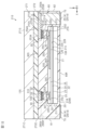
- Second Embodiment The configuration of a semiconductor device 210 of the second embodiment will be described with reference to Figures 13 to 18.
- the semiconductor device 210 is mounted on a substrate 920 in place of the semiconductor device 10 shown in Figure 2.
- the semiconductor device 210 of the second embodiment is different from the semiconductor device 10 of the first embodiment in the structure of a conductive portion 240 to which a semiconductor element 20 is connected.
- components common to the first embodiment are denoted by the same reference numerals, and description thereof will be omitted.
- FIGS. 13 and 14 are perspective views showing the external appearance of the semiconductor device 210, with FIG. 13 being a perspective view of the semiconductor device 210 seen from the top, and FIG. 14 being a perspective view of the semiconductor device 210 seen from the bottom.
- FIG. 15 is a plan view of the semiconductor device 210 seen from the bottom. Note that FIG. 15 shows the sealing resin 280 through the view.
- FIG. 16 is a plan view showing the conductive portion 240.
- FIG. 17 is a schematic cross-sectional view of the semiconductor device 210 taken along line 17-17 in FIG. 15.
- FIG. 18 is a schematic cross-sectional view of the semiconductor device 210 taken along line 18-18 in FIG. 15. Note that for the sake of convenience, FIGS. 17 and 18 may show components that are not on the line indicating the cross-sectional position, or the positions and sizes of components may differ from those in FIGS. 15 and 16.
- the semiconductor device 210 has, for example, a rectangular parallelepiped shape. As shown in FIGS. 13 to 18 , the semiconductor device 210 includes a substrate 271 , a substrate insulating film 272 , a semiconductor element 20 , a conductive portion 240 , and a sealing resin 280 .
- the conductive portion 240 includes a second coil 243 and external connection terminals 251A, 251B, 261A, and 261B.
- the semiconductor element 20 is mounted on the conductive portion 240.
- the first coil 26 of the semiconductor element 20 faces the second coil 243 of the conductive portion 240 in the z-direction.
- the first coil 26 and the second coil 243 correspond to the coils 913A and 913B shown in FIG. 1.
- the semiconductor device 210 includes an external conductive film 70 that covers the external connection terminals 251A, 251B, 261A, and 261B.
- the semiconductor device 210 includes a device top surface 10S, a device bottom surface 10R, and a number of device side surfaces 11, 12, 13, and 14.
- the substrate 271 is formed in a rectangular plate shape in a plan view.
- the substrate 271 may have insulating properties.
- the substrate 271 may be a semiconductor substrate, for example.
- the substrate 271 is formed of a material containing Si, for example.
- the substrate 271 includes an upper surface 271S, a lower surface 271R, and multiple side surfaces 271C.
- the upper surface 271S and the lower surface 271R face opposite each other in the z direction.
- the multiple side surfaces 271C intersect with the upper surface 271S and the lower surface 271R.
- the multiple side surfaces 271C face either in the x direction or the y direction.
- the upper surface 271S of the substrate 271 constitutes the device upper surface 10S of the semiconductor device 210.
- the multiple side surfaces 271C constitute device side surfaces 11 to 14 of the semiconductor device 210.
- the substrate insulating film 272 is provided on a lower surface 271R of the substrate 271.
- the substrate insulating film 272 is formed to have the same size as the substrate 271 in a plan view.
- the substrate insulating film 272 includes an upper surface 272S, a lower surface 272R, and multiple side surfaces 272C.
- the upper surface 272S and the lower surface 272R face in opposite directions in the z direction.
- the multiple side surfaces 272C intersect with the upper surface 272S and the lower surface 272R.
- the multiple side surfaces 272C face in either the x direction or the y direction.
- the upper surface 272S of the substrate insulating film 272 contacts the lower surface 272R of the substrate 271.
- the multiple side surfaces 272C constitute device side surfaces 11 to 14 of the semiconductor device 210.
- the substrate insulating film 272 is formed of, for example, a material containing Si.
- the substrate insulating film 272 is made of SiO 2 , SiN, etc.
- the substrate insulating film 272 may be made of a plurality of insulating films.
- the sealing resin 280 is provided on the lower surface 272R of the substrate insulating film 272.
- the sealing resin 280 is formed to have the same size as the substrate 271 and the substrate insulating film 272 in a plan view.
- the sealing resin 280 includes a resin upper surface 80S, a resin lower surface 80R, and multiple resin side surfaces 81-84.
- the resin upper surface 80S of the sealing resin 280 contacts the lower surface 272R of the substrate insulating film 272. It can be said that the semiconductor device 210 includes the substrate 271, the substrate insulating film 272 laminated on the lower surface 271R of the substrate 271, and the sealing resin 280.
- the sealing resin 280 seals the semiconductor element 20, the conductive portion 240, and the joint portion SD.
- the sealing resin 280 covers the element front surface 20S, the element back surface 20R, and the element side surfaces 201 to 204 of the semiconductor element 20. Therefore, it can be said that the semiconductor element 20 is embedded in the sealing resin 280.
- the semiconductor element 20 is disposed in the sealing resin 280 so that the element front surface 20S faces the same direction as the resin upper surface 80S of the sealing resin 280. Therefore, the element front surface 20S of the semiconductor element 20 faces the lower surface 272R of the substrate insulating film 272.
- the sealing resin 280 is made of, for example, a resin having electrical insulation properties.
- a synthetic resin containing an epoxy resin as a main component can be used.
- a synthetic resin containing a filler can be used.
- the filler is made of, for example, SiO2 .
- the sealing resin 280 is colored, for example, black. Note that the material and shape of the sealing resin 280 are not limited.
- the conductive portion 240 includes a first wiring member 241, a second wiring member 242, and a second coil 243.
- the conductive portion 240 may be formed of, for example, a plating layer.
- the conductive portion 240 is formed of, for example, a material containing Cu.
- the first wiring member 241 includes a first external connection terminal 251A, a second external connection terminal 251B, a first element connection portion 253A, a second element connection portion 253B, a first connection wiring 254A, a second connection wiring 254B, a first terminal connection portion 255A, and a second terminal connection portion 255B.
- the first element connection portion 253A, the second element connection portion 253B, the first connection wiring 254A, the second connection wiring 254B, the first terminal connection portion 255A, and the second terminal connection portion 255B configure a "first lead-out wiring.”
- the first element connection portion 253A, the first connection wiring 254A, and the first terminal connection portion 255A are formed on the lower surface 272R of the substrate insulating film 272.
- the first element connection portion 253A is electrically connected to the first terminal connection portion 255A by the first connection wiring 254A.
- the first element connection portion 253A, the first connection wiring 254A, and the first terminal connection portion 255A may be an integrally formed one piece.
- the second element connection portion 253B, the second connection wiring 254B, and the second terminal connection portion 255B are formed on the lower surface 272R of the substrate insulating film 272.
- the second element connection portion 253B is electrically connected to the second terminal connection portion 255B by the second connection wiring 254B.
- the second element connection portion 253B, the second connection wiring 254B, and the second terminal connection portion 255B may be an integrally formed one piece.
- the first element connection portion 253A and the second element connection portion 253B are arranged at positions overlapping the semiconductor element 20 in a plan view.
- the first element connection portion 253A and the second element connection portion 253B are arranged at positions overlapping the element electrodes 31A, 31B of the semiconductor element 20 in the z direction.
- the first element connection portion 253A and the second element connection portion 253B are formed in a rectangular shape when viewed in a plane. Note that the shape of the first element connection portion 253A and the second element connection portion 253B can be changed to any shape, such as a circle or a polygon, when viewed in a plane.
- the first element connection portion 253A is electrically connected to the first element electrode 31A of the semiconductor element 20 via a joint SD.
- the second element connection portion 253B is electrically connected to the second element electrode 31B of the semiconductor element 20 via a joint SD.
- the first external connection terminal 251A is provided on the lower surface 255R of the first terminal connection portion 255A.
- the first external connection terminal 251A is electrically connected to the first terminal connection portion 255A.
- the first external connection terminal 251A extends from the first terminal connection portion 255A toward the resin lower surface 80R of the sealing resin 280.
- the lower surface 251A1 of the first external connection terminal 251A is exposed from the resin lower surface 80R of the sealing resin 280.
- the second external connection terminal 251B is provided on the lower surface 255R of the second terminal connection portion 255B.
- the second external connection terminal 251B is electrically connected to the second terminal connection portion 255B.
- the second external connection terminal 251B extends from the second terminal connection portion 255B toward the resin lower surface 80R of the sealing resin 280.
- the lower surface 251B1 of the second external connection terminal 251B is exposed from the resin lower surface 80R of the sealing resin 280.
- the first external connection terminal 251A and the second external connection terminal 251B are formed in a rectangular shape when viewed in a plane. Note that the shape of the first external connection terminal 251A and the second external connection terminal 251B can be changed to any shape, such as a circle or a polygon, when viewed in a plane.
- the first external connection terminal 251A and the second external connection terminal 251B are arranged along the device side surface 12 of the semiconductor device 210, in one example.
- the first external connection terminal 251A and the second external connection terminal 251B are arranged at a distance in the y direction.
- the first external connection terminal 251A and the second external connection terminal 251B are arranged side by side in the y direction in a plan view.
- the first external connection terminal 251A is arranged at a corner portion formed by the device side surface 12 and the device side surface 14 of the semiconductor device 210.
- the second external connection terminal 251B is arranged at a corner portion formed by the device side surface 12 and the device side surface 13 of the semiconductor device 210.
- the second coil 243 is formed on the lower surface 272R of the substrate insulating film 272. As shown in Fig. 15 and Fig. 16, the second coil 243 is formed in a spiral shape in a plan view. As shown in Fig. 15, the second coil 243 is disposed so as to overlap with the first coil 26 of the semiconductor element 20 in a plan view.
- the second wiring member 242 includes a third external connection terminal 261A, a fourth external connection terminal 261B, a third connection wiring 264A, a fourth connection wiring 264B, a third terminal connection portion 265A, a fourth terminal connection portion 265B, and an end connection portion 266.
- the third connection wiring 264A, the fourth connection wiring 264B, the third terminal connection portion 265A, and the fourth terminal connection portion 265B configure a "second lead-out wiring.”
- the second coil 243 is formed in a spiral shape in a plan view.
- the second coil 243 includes an outer first end 243A and an inner second end 243B.
- the first end 243A corresponds to the "outer end”.
- the second end 243B corresponds to the "inner end”.
- the end connection portion 266 is disposed inside the second coil 243.
- the end connection portion 266 is electrically connected to the second end 243B of the second coil 243.
- the first end 243A of the second coil 243 is electrically connected to the third terminal connection portion 265A by the third connection wiring 264A.
- the second coil 243, the end connection portion 266, the third connection wiring 264A, and the third terminal connection portion 265A may be an integrally formed one piece.
- the end connection portion 266 is electrically connected to the fourth terminal connection portion 265B by the fourth connection wiring 264B.
- the fourth connection wiring 264B is embedded in the substrate insulating film 272.
- the fourth connection wiring 264B includes an embedded wiring 267 and vias 268A and 268B. A first end of the embedded wiring 267 is electrically connected to the end connection portion 266 by the via 268A. A second end of the embedded wiring 267 is electrically connected to the fourth terminal connection portion 265B by the via 268B.
- the third external connection terminal 261A is provided on the lower surface 265R of the third terminal connection portion 265A.
- the third external connection terminal 261A is electrically connected to the third terminal connection portion 265A.
- the third external connection terminal 261A extends from the third terminal connection portion 265A toward the resin lower surface 80R of the sealing resin 280.
- the lower surface 261A1 of the third external connection terminal 261A is exposed from the sealing resin 280.
- the fourth external connection terminal 261B is provided on the lower surface 265R of the fourth terminal connection portion 265B.
- the fourth external connection terminal 261B is electrically connected to the fourth terminal connection portion 265B.
- the fourth external connection terminal 261B extends from the fourth terminal connection portion 265B toward the resin lower surface 80R of the sealing resin 280.
- the lower surface 261B1 of the fourth external connection terminal 261B is exposed from the sealing resin 280.
- the third and fourth external connection terminals 261A and 261B are formed in a rectangular shape in a plan view. Note that the shape of the third and fourth external connection terminals 261A and 261B can be changed to any shape, such as a circular shape or a polygonal shape, in a plan view.
- the third external connection terminal 261A and the fourth external connection terminal 261B are arranged along the device side surface 11 of the semiconductor device 210, in one example.
- the third external connection terminal 261A and the fourth external connection terminal 261B are arranged at a distance in the y direction.
- the first external connection terminal 251A and the second external connection terminal 251B are arranged side by side in the y direction in a plan view.
- the third external connection terminal 261A is arranged at a corner portion formed by the device side surface 11 and the device side surface 14 of the semiconductor device 210.
- the fourth external connection terminal 261B is arranged at a corner portion formed by the device side surface 11 and the device side surface 13 of the semiconductor device 210.
- the external conductive film 70 is formed so as to cover the lower surfaces 251A1, 251B1, 261A1, and 261B1 of the external connection terminals 251A, 251B, 261A, and 261B, respectively.
- the external conductive film 70 is composed of, for example, a plurality of metal layers stacked on top of each other.
- the metal layers are, for example, Ni layers, Pd layers, and Au layers.
- the material of the external conductive film is not limited, but may be, for example, Ni layers and Au layers stacked on top of each other, or Sn.
- the conductive portion 240 is formed, for example, by a plating layer.
- This semiconductor device 210 can be made smaller than the semiconductor device 10 in which the conductive portion 40 is formed by a lead frame.
- the semiconductor device 310 includes a sealing resin 380.
- the resin side surfaces 81, 82 of the sealing resin 380 include first side surfaces 81A, 82A and second side surfaces 81B, 82B, respectively.
- the first side surfaces 81A, 82A are disposed closer to the resin upper surface 80S than the resin lower surface 80R in the z direction.
- the second side surfaces 81B, 82B are disposed closer to the resin lower surface 80R than the resin upper surface 80S in the z direction.
- the second side surfaces 81B, 82B of the resin side surfaces 81, 82 are located inside the sealing resin 380 with respect to the first side surfaces 81A, 82A of the resin side surfaces 81, 82 in a plan view.
- the sealing resin is formed so that the side of the resin upper surface 80S is larger than the side of the resin lower surface 80R in the z direction.
- the first side surfaces 81A, 82A of the resin side surfaces 81, 82 are perpendicular to the resin upper surface 80S.
- the second side surfaces 81B, 82B of the resin side surfaces 81, 82 are perpendicular to the resin lower surface 80R.
- the sealing resin 380 has a step 383 that is recessed toward the inside of the sealing resin 380 in a plan view due to the positions of the first side surfaces 81A, 82A and the second side surfaces 81B, 82B of the resin side surfaces 81, 82.
- the first external connection terminal 251A is exposed from the second side surface 82B of the resin side surface 82 in the x direction. That is, the first external connection terminal 251A is exposed to the resin lower surface 80R of the sealing resin 380 and the second side surface 82B of the resin side surface 82.
- the first external connection terminal 251A includes a lower surface 251A1 and a side surface 251A2 exposed from the sealing resin 380.
- the lower surface 251A1 and the side surface 251A2 of the first external connection terminal 251A are covered by an external conductive film 70.
- the external conductive film 70 includes a first conductive film 70A covering the lower surface 251A1 of the first external connection terminal 251A and a second conductive film 70B covering the side surface 251A2 of the first external connection terminal 251A.
- the second external connection terminal 251B is exposed from the second side surface 82B of the resin side surface 82 in the x direction. That is, the second external connection terminal 251B is exposed to the resin lower surface 80R of the sealing resin 380 and the second side surface 82B of the resin side surface 82.
- the second external connection terminal 251B includes a lower surface 251B1 and a side surface 251B2 exposed from the sealing resin 380.
- the lower surface 251B1 and the side surface 251B2 of the second external connection terminal 251B are covered by an external conductive film 70.
- the external conductive film 70 includes a first conductive film 70A covering the lower surface 251B1 of the second external connection terminal 251B and a second conductive film 70B covering the side surface 251B2 of the first external connection terminal 251A.
- the third external connection terminal 261A is exposed from the second side surface 81B of the resin side surface 81 in the x direction. That is, the third external connection terminal 261A is exposed to the resin lower surface 80R of the sealing resin 380 and the second side surface 81B of the resin side surface 81.
- the third external connection terminal 261A includes a lower surface 261A1 and a side surface 261A2 exposed from the sealing resin 380.
- the lower surface 261A1 and the side surface 261A2 of the third external connection terminal 261A are covered by an external conductive film 70.
- the external conductive film 70 includes a first conductive film 70A covering the lower surface 261A1 of the third external connection terminal 261A and a second conductive film 70B covering the side surface 261A2 of the first external connection terminal 251A.
- the fourth external connection terminal 261B is exposed from the second side surface 81B of the resin side surface 81 in the x direction. That is, the fourth external connection terminal 261B is exposed to the resin lower surface 80R of the sealing resin 380 and the second side surface 81B of the resin side surface 81.
- the fourth external connection terminal 261B includes a lower surface 261B1 and a side surface 261B2 exposed from the sealing resin 380.
- the lower surface 261B1 and the side surface 261B2 of the fourth external connection terminal 261B are covered by an external conductive film 70.
- the external conductive film 70 includes a first conductive film 70A covering the lower surface 261B1 of the fourth external connection terminal 261B and a second conductive film 70B covering the side surface 261B2 of the first external connection terminal 251A.
- the modified semiconductor device 310 is mounted on the substrate 920 shown in FIG. 2.
- the solder connecting the external connection terminals 251A, 251B, 261A, and 261B to the mounting pads of the substrate 920 adheres to the first conductive film 70A and the second conductive film 70B that cover the external conductive film 70.
- the liquid-phase solder creeps up the second conductive film 70B and forms a solder fillet between the second conductive film 70B and the mounting pad.
- the solder fillet is easily formed in the semiconductor device 310.
- This solder fillet increases the solder joint area and increases the connection strength.
- the solder fillet also makes it easier to check the soldering state of the semiconductor device 310.
- the step 383 may be provided on each of the resin side surfaces 81 to 84.
- the external connection terminal may be exposed from the second side surface that constitutes the step provided on each of the resin side surfaces 81 to 84.
- the side surface of the external connection terminal that is exposed from the second side surface may be covered with an external conductive film.
- the configuration of a semiconductor device 410 of the third embodiment will be described with reference to Figures 23 to 28.
- the semiconductor device 410 is mounted on a substrate 920 instead of the semiconductor device 10 shown in Figure 2.
- the semiconductor device 410 of the third embodiment is different from the semiconductor devices 10 and 210 in the structure of a conductive part 440 to which a semiconductor element 20 is connected.
- components common to the first and second embodiments are denoted by the same reference numerals, and description thereof will be omitted.
- FIGS. 23 and 24 are perspective views showing the external appearance of the semiconductor device 410, where FIG. 23 is a perspective view of the semiconductor device 410 seen from the top, and FIG. 24 is a perspective view of the semiconductor device 410 seen from the bottom.
- FIG. 25 is a plan view of the semiconductor device 410 seen from the bottom. Note that in FIGS. 25 and 26, the sealing resin 480 is shown through the view.
- FIG. 26 is a plan view showing the conductive portion 440.
- FIG. 27 is a schematic cross-sectional view of the semiconductor device 410 taken along line 27-27 in FIG. 25.
- FIG. 28 is a schematic cross-sectional view of the semiconductor device 410 taken along line 28-28 in FIG. 15. Note that for the sake of convenience, in FIGS. 27 and 28, members that are not on the line indicating the cross-sectional position may be shown, or the positions and sizes of members may differ from those in FIGS. 25 and 26.
- the semiconductor device 410 has, for example, a rectangular parallelepiped shape. As shown in FIGS. 23 to 28 , a semiconductor device 410 includes a semiconductor element 20 , a conductive portion 440 , a sealing resin 480 , and a resin layer 470 .
- the conductive portion 440 includes a second coil 443 and external connection terminals 451A, 451B, 461A, and 461B.
- the semiconductor element 20 is mounted on the conductive portion 440.
- the first coil 26 of the semiconductor element 20 faces the second coil 443 of the conductive portion 440 in the z-direction.
- the first coil 26 and the second coil 443 correspond to the coils 913A and 913B shown in FIG. 1.
- the semiconductor device 410 includes an external conductive film 70 that covers the external connection terminals 451A, 451B, 461A, and 461B.
- the semiconductor device 410 includes a device top surface 10S, a device bottom surface 10R, and a number of device side surfaces 11, 12, 13, and 14.
- the sealing resin 480 is formed in a rectangular plate shape.
- the sealing resin 480 includes a resin upper surface 80S, a resin lower surface 80R, and a plurality of resin side surfaces 81 to 84.
- the resin upper surface 80S of the sealing resin 480 constitutes the device upper surface 10S of the semiconductor device 410.
- the sealing resin 480 seals the semiconductor element 20, the conductive portion 440, and the joint portion SD.
- the sealing resin 480 covers the element front surface 20S, the element rear surface 20R, and the element side surfaces 201 to 204 of the semiconductor element 20. Therefore, it can be said that the semiconductor element 20 is embedded in the sealing resin 480.
- the semiconductor element 20 is disposed in the sealing resin 480 so that the element front surface 20S faces in the same direction as the resin bottom surface 80R of the sealing resin 480.
- the sealing resin 480 is made of, for example, a resin having electrical insulation properties.
- a synthetic resin containing an epoxy resin as a main component can be used.
- a synthetic resin containing a filler can be used.
- the filler is made of, for example, SiO2 .
- the sealing resin 480 is colored, for example, black. Note that the material and shape of the sealing resin 480 are not limited.
- the resin layer 470 is formed in a rectangular plate shape in a plan view, and is formed to have the same size as the sealing resin 480 in a plan view.
- the resin layer 470 has insulating properties.
- the resin layer 470 is the base member of the semiconductor device 410.
- the semiconductor element 20 is mounted on the resin layer 470.
- the resin layer 470 can be said to be a support member that supports the semiconductor element 20.
- the resin layer 470 includes an upper surface 470S, a lower surface 470R, and multiple side surfaces 471, 472, 473, and 474.
- the upper surface 470S and the lower surface 470R face opposite each other in the z direction.
- the upper surface 470S of the resin layer 470 contacts the resin lower surface 80R of the sealing resin 480.
- the lower surface 470R of the resin layer 470 faces the same direction as the resin lower surface 80R of the sealing resin 480.
- the side surfaces 471 to 474 of the resin layer 470 intersect with the upper surface 470S and the lower surface 470R of the resin layer 470.
- the side surfaces 471, 472 of the resin layer 470 face opposite each other in the x direction.
- the side surfaces 473, 474 of the resin layer 470 face opposite each other in the y direction.
- the bottom surface 470R of the resin layer 470 constitutes the device bottom surface 10R of the semiconductor device 410.
- the resin side surfaces 81-84 of the sealing resin 480 and the side surfaces 471-474 of the resin layer 470 constitute the device side surfaces 11-14 of the semiconductor device 410.
- the resin layer 470 is made of, for example, a resin having electrical insulation properties.
- a synthetic resin mainly composed of an epoxy resin can be used.
- a synthetic resin containing a filler can be used for the resin layer 470.
- the filler is made of, for example, SiO 2.
- the resin layer 470 is colored, for example, black.
- the material and shape of the resin layer 470 are not limited.
- the resin layer 470 may be made of the same material as the sealing resin 480.
- the interface between the sealing resin 480 and the resin layer 470 (the resin lower surface 80R of the sealing resin 480 and the upper surface 470S of the resin layer 470) may not be formed when the resin layer 470 and the sealing resin 480 are made of the same material.
- the conductive portion 440 includes a first wiring member 441, a second wiring member 442, and a second coil 443.
- the conductive portion 440 may be formed of, for example, a plating layer.
- the conductive portion 240 is formed of, for example, a material containing Cu.
- the first wiring member 441 includes a first external connection terminal 451A, a second external connection terminal 451B, a first element connection portion 453A, a second element connection portion 453B, a first connection wiring 454A, a second connection wiring 454B, a first terminal connection portion 455A, and a second terminal connection portion 455B.
- the first element connection portion 453A, the second element connection portion 453B, the first connection wiring 454A, the second connection wiring 454B, the first terminal connection portion 455A, and the second terminal connection portion 455B configure a "first lead-out wiring.”
- the first element connection portion 453A, the first connection wiring 454A, and the first terminal connection portion 455A are formed on the upper surface 470S of the resin layer 470.
- the first element connection portion 453A is electrically connected to the first terminal connection portion 455A by the first connection wiring 454A.
- the first element connection portion 453A, the first connection wiring 454A, and the first terminal connection portion 455A may be an integrally formed one piece.
- the second element connection portion 453B, the second connection wiring 454B, and the second terminal connection portion 455B are formed on the upper surface 470S of the resin layer 470.
- the second element connection portion 453B is electrically connected to the second terminal connection portion 455B by the second connection wiring 454B.
- the second element connection portion 453B, the second connection wiring 454B, and the second terminal connection portion 455B may be an integrally formed one piece.
- the first element connection portion 453A and the second element connection portion 453B are arranged at positions overlapping the semiconductor element 20 in a plan view.
- the first element connection portion 453A and the second element connection portion 453B are arranged at positions overlapping the element electrodes 31A, 31B of the semiconductor element 20 in the z direction.
- the first element connection portion 453A and the second element connection portion 453B are formed in a rectangular shape in a plan view. Note that the shape of the first element connection portion 453A and the second element connection portion 453B can be changed to any shape, such as a circle or a polygon, in a plan view.
- a barrier layer 47 is formed on the first element connection portion 453A.
- the first element connection portion 453A is electrically connected to the first element electrode 31A of the semiconductor element 20 by the barrier layer 47 and a joint SD.
- a barrier layer 47 is formed on the second element connection portion 453B.
- the second element connection portion 453B is electrically connected to the second element electrode 31B of the semiconductor element 20 by the barrier layer 47 and a joint SD.
- the first external connection terminal 451A is electrically connected to the first terminal connection portion 455A.
- the first external connection terminal 451A extends from the first terminal connection portion 455A toward the resin lower surface 80R of the sealing resin 480.
- the lower surface 451A1 of the first external connection terminal 451A is exposed from the lower surface 470R of the resin layer 470.
- the second external connection terminal 451B is electrically connected to the second terminal connection portion 455B.
- the second external connection terminal 451B extends from the second terminal connection portion 455B toward the resin lower surface 80R of the sealing resin 480.
- the lower surface 451B1 of the second external connection terminal 451B is exposed from the lower surface 470R of the resin layer 470.
- the first external connection terminal 451A and the second external connection terminal 451B are formed in a rectangular shape when viewed in a plane.
- the shape of the first external connection terminal 451A and the second external connection terminal 451B can be changed to any shape, such as a circular shape or a polygonal shape, when viewed in a plane.
- the first external connection terminal 451A and the second external connection terminal 451B are arranged along the device side surface 12 of the semiconductor device 410, in one example.
- the first external connection terminal 451A and the second external connection terminal 451B are arranged at a distance in the y direction.
- the first external connection terminal 451A and the second external connection terminal 451B are arranged side by side in the y direction in a plan view.
- the first external connection terminal 451A is arranged at a corner portion formed by the device side surface 12 and the device side surface 13 of the semiconductor device 410.
- the second external connection terminal 451B is arranged at a corner portion formed by the device side surface 12 and the device side surface 14 of the semiconductor device 410.
- the second wiring member 442 includes a third external connection terminal 461A, a fourth external connection terminal 461B, a third connection wiring 464A, a fourth connection wiring 464B, a third terminal connection portion 465A, a fourth terminal connection portion 465B, and an end connection portion 466.
- the third connection wiring 464A, the fourth connection wiring 464B, the third terminal connection portion 465A, the fourth terminal connection portion 465B, and the end connection portion 466 configure a "second lead-out wiring.”
- the second coil 443 is formed on the upper surface 470S of the resin layer 470. As shown in FIG. 25 and FIG. 26, the second coil 443 is formed in a spiral shape in a planar view. As shown in FIG. 25, the second coil 443 is arranged so as to overlap with the first coil 26 of the semiconductor element 20 in a planar view.
- the second coil 443 includes an outer first end 443A and an inner second end 443B.
- the first end 443A corresponds to the "outer end”.
- the second end 443B corresponds to the "inner end”.
- the end connection portion 466 is disposed inside the second coil 443.
- the end connection portion 466 is electrically connected to the second end 443B of the second coil 443.
- the first end 443A of the second coil 443 is electrically connected to the third terminal connection portion 465A by the third connection wiring 464A.
- the second coil 443, the end connection portion 466, the third connection wiring 464A, and the third terminal connection portion 465A may be an integrally formed one piece.
- the end connection portion 466 is electrically connected to the fourth terminal connection portion 465B by the fourth connection wiring 464B.
- the fourth connection wiring 464B is embedded in a resin layer 470.
- the fourth connection wiring 464B includes an embedded wiring 467 and vias 468A connected to both ends of the embedded wiring 467. A first end of the embedded wiring 467 is electrically connected to the end connection portion 466 by the via 468A. A second end of the embedded wiring 467 is electrically connected to the fourth terminal connection portion 465B (see FIG. 26) by the via 468A.
- the third external connection terminal 461A is provided on the lower surface 465R of the third terminal connection portion 465A.
- the third external connection terminal 461A is electrically connected to the third terminal connection portion 465A.
- the third external connection terminal 461A extends from the third terminal connection portion 465A toward the lower surface 470R of the resin layer 470.
- the lower surface 461A1 of the third external connection terminal 461A is exposed from the lower surface 470R of the resin layer 470.
- the fourth external connection terminal 461B is provided on the lower surface 465R of the fourth terminal connection portion 465B.
- the fourth external connection terminal 461B is electrically connected to the fourth terminal connection portion 465B.
- the fourth external connection terminal 461B extends from the fourth terminal connection portion 465B toward the lower surface 470R of the resin layer 470.
- the lower surface 461B1 of the fourth external connection terminal 461B is exposed from the lower surface 470R of the resin layer 470.
- the third external connection terminal 461A and the fourth external connection terminal 461B are formed in a rectangular shape in a plan view. Note that the shape of the third external connection terminal 461A and the fourth external connection terminal 461B can be changed to any shape, such as a circular shape or a polygonal shape, in a plan view.
- the third external connection terminal 461A and the fourth external connection terminal 461B are arranged along the device side surface 11 of the semiconductor device 410, in one example.
- the third external connection terminal 461A and the fourth external connection terminal 461B are arranged at a distance in the y direction.
- the first external connection terminal 451A and the second external connection terminal 451B are arranged side by side in the y direction in a plan view.
- the third external connection terminal 461A is arranged at a corner portion formed by the device side surface 11 and the device side surface 13 of the semiconductor device 410.
- the fourth external connection terminal 461B is arranged at a corner portion formed by the device side surface 11 and the device side surface 14 of the semiconductor device 410.
- the semiconductor device 410 includes external connection terminals 451A, 451B, 461A, and 461B that penetrate the resin layer 470.
- the device top surface 10S of the semiconductor device 410 is formed by the resin top surface 80S of the sealing resin 480 that seals the semiconductor element 20. Therefore, it is possible to achieve a smaller size (lower profile) than the semiconductor device 210 that includes the substrate 271 and substrate insulating film 272.
- the semiconductor device 510 includes a sealing resin 580.
- the resin side surfaces 83 and 84 of the sealing resin 580 include first side surfaces 83A and 84A and second side surfaces 83B and 84B, respectively.
- the first side surfaces 83A and 84A are disposed closer to the resin upper surface 80S than the resin lower surface 80R in the z direction.
- the second side surfaces 83B and 84B are disposed closer to the resin lower surface 80R than the resin upper surface 80S in the z direction.
- the second side surfaces 83B and 84B of the resin side surfaces 83 and 84 are located inside the sealing resin 580 with respect to the first side surfaces 83A and 84A of the resin side surfaces 83 and 84 in a plan view.
- the sealing resin is formed so that the side of the resin upper surface 80S is larger than the side of the resin lower surface 80R in the z direction.
- the first side surfaces 83A, 84A of the resin side surfaces 83, 84 are perpendicular to the resin upper surface 80S.
- the second side surfaces 83B, 84B of the resin side surfaces 83, 84 are perpendicular to the resin lower surface 80R.
- the sealing resin 580 has a step 583 that is recessed toward the inside of the sealing resin 580 in a plan view due to the positions of the first side surfaces 83A, 84A and the second side surfaces 83B, 84B of the resin side surfaces 83, 84.
- the step 583 may be provided on the resin side surfaces 81 to 84.
- the resin layer 470 When viewed from the z direction, the resin layer 470 is formed to have the same size as the resin underside 80R of the sealing resin 580. Therefore, when viewed from the z direction, the side surfaces 473, 474 of the resin layer 470 facing the y direction are located inside the resin layer 470 relative to the first side surfaces 83A, 84A of the sealing resin 580. If the step 583 is provided on the resin side surfaces 81, 82, the positions of the side surfaces 471, 472 are changed accordingly.
- the first external connection terminal 551A is exposed from the side surface 473 of the resin layer 470 in the y direction. That is, the first external connection terminal 551A is exposed from the lower surface 470R and the side surface 473 of the resin layer 470.
- the first external connection terminal 551A includes a lower surface 551A1 and a side surface 551A2 exposed from the resin layer 470.
- the lower surface 551A1 and the side surface 551A2 of the first external connection terminal 551A are covered by an external conductive film 70.
- the external conductive film 70 includes a first conductive film 70A covering the lower surface 551A1 of the first external connection terminal 551A and a second conductive film 70B covering the side surface 551A2 of the first external connection terminal 551A.
- the second external connection terminal 551B is exposed from the side surface 474 of the resin layer 470 in the y direction. That is, the second external connection terminal 551B is exposed from the lower surface 470R and the side surface 474 of the resin layer 470.
- the second external connection terminal 551B includes a lower surface 551B1 and a side surface 551B2 exposed from the resin layer 470.
- the lower surface 551B1 and the side surface 551B2 of the second external connection terminal 551B are covered by an external conductive film 70.
- the external conductive film 70 includes a first conductive film 70A covering the lower surface 551B1 of the second external connection terminal 551B and a second conductive film 70B covering the side surface 551B2 of the first external connection terminal 551A.
- the third external connection terminal 561A is exposed from the side surface 473 of the resin layer 470 in the y direction. That is, the third external connection terminal 561A is exposed from the lower surface 470R and the side surface 473 of the resin layer 470.
- the third external connection terminal 561A includes a lower surface 561A1 and a side surface 561A2 exposed from the resin layer 470.
- the lower surface 561A1 and the side surface 561A2 of the third external connection terminal 561A are covered by an external conductive film 70.
- the external conductive film 70 includes a first conductive film 70A covering the lower surface 561A1 of the third external connection terminal 561A and a second conductive film 70B covering the side surface 561A2 of the first external connection terminal 551A.
- the fourth external connection terminal 561B is exposed from the side surface 474 of the resin layer 470 in the y direction. That is, the fourth external connection terminal 561B is exposed from the lower surface 470R and the side surface 474 of the resin layer 470.
- the fourth external connection terminal 561B includes a lower surface 561B1 and a side surface 561B2 exposed from the resin layer 470.
- the lower surface 561B1 and the side surface 561B2 of the fourth external connection terminal 561B are covered by an external conductive film 70.
- the external conductive film 70 includes a first conductive film 70A covering the lower surface 561B1 of the fourth external connection terminal 561B and a second conductive film 70B covering the side surface 561B2 of the first external connection terminal 551A.
- the semiconductor device 510 of the modified example is mounted on the substrate 920 shown in FIG. 2.
- the solder connecting each of the external connection terminals 551A, 551B, 561A, and 561B to the mounting pads of the substrate 920 adheres to the first conductive film 70A and the second conductive film 70B covering the external connection terminals 551A, 551B, 561A, and 561B.
- the liquid-phase solder creeps up the second conductive film 70B and forms a solder fillet between the second conductive film 70B and the mounting pad.
- the solder fillet is easily formed in the semiconductor device 510.
- This solder fillet increases the solder joint area and increases the connection strength.
- the solder fillet also makes it easier to check the soldering state of the semiconductor device 510.
- 29 and 30 show a case where the external connection terminals 551A and 561A are exposed on the side surface 473 of the resin layer 470, and the external connection terminals 551B and 561B are exposed on the side surface 474 of the resin layer 470.
- the side surface to which the external connection terminals 551A, 551B, 561A, and 561B are exposed can be changed as desired.
- the external connection terminals 551A and 551B can be exposed on the side surface 472 of the resin layer 470, and the external connection terminals 561A and 561B can be exposed on the side surface 471 of the resin layer 470.
- the external connection terminal 551A can also be exposed on two adjacent side surfaces, such as the side surface 472 and the side surface 473 of the resin layer 470. Similarly, the external connection terminals 551B, 561A, and 561B can also be exposed on two adjacent side surfaces.
- Figs. 31 and 32 The overall shape, the arrangement and shape of the terminals, etc., of the semiconductor devices 10, 110, 210, 310, 410, and 510 of the above-mentioned embodiments and modifications can be arbitrarily modified.
- a modification of the semiconductor device 410 of the third embodiment is shown in Figs. 31 and 32.
- Fig. 31 is a plan view of the semiconductor device 610 of the modification, viewed from the bottom side.
- Fig. 32 is a schematic cross-sectional view showing the external connection terminals 451A and 451B connected to the semiconductor element 620 in the semiconductor device 610 of the modification.
- connection wiring 630 is electrically connected to the connection pads 27A, 27B exposed from the opening 25X of the third insulating layer 25 of the element insulating layer 22.
- the connection wiring 630 extends from the connection pads 27A, 27B to the insulating surface 22S of the element insulating layer 22.
- the connection wiring 630 is sometimes called a redistribution layer.
- the element electrodes 31A, 31B are electrically connected to the portion of the connection wiring 630 arranged on the insulating surface 22S of the element insulating layer 22.
- the element electrodes 31C and 31D are arranged so as to overlap the connection pads 27C and 27D in a plan view. As with the element electrodes 31A and 31B, these element electrodes 31C and 31D may also be arranged so as not to overlap the connection pads 27C and 27D.
- a semiconductor element capacitor chip that uses a capacitor to provide insulation between the first circuit 911 and the second circuit 912 can be used.
- a capacitor chip that includes a capacitor is an example of a semiconductor device that includes an insulated configuration.
- FIG. 33 is a schematic plan view of a semiconductor device 710 including a capacitor
- FIG. 34 shows a schematic cross-sectional view of the semiconductor device 710 of FIG.
- the semiconductor device 710 includes a semiconductor element 720.
- the semiconductor element 720 includes a first electrode plate 726.
- the first electrode plate 726 is electrically connected to an element electrode 31B by an element wiring 728.
- a first end 728A of the element wiring 728 is electrically connected to the first electrode plate 726 by a via 729A.
- a second end 728B of the element wiring 728 is electrically connected to a connection pad 27B by a via 729B.
- the element electrode 31B is connected to the connection pad 27B.
- a second electrode plate 743 is disposed on the upper surface 470S of the resin layer 470 of the semiconductor device 710.
- the conductive portion 740 includes a first wiring member 741, a second wiring member 742, and a second electrode plate 743.
- the first wiring member 741 includes an external connection terminal 451A, a second external connection terminal 451B, a first element connection portion 453A, a second element connection portion 453B, a second connection wiring 454B, a first terminal connection portion 455A, and a second terminal connection portion 455B.
- the second wiring member 742 includes a third external connection terminal 461A, a fourth external connection terminal 461B, a third connection wiring 464A, a third terminal connection portion 465A, and a fourth terminal connection portion 465B.
- the first electrode plate 726 and the second electrode plate 743 face each other in the z direction.
- the first electrode plate 726 and the second electrode plate 743 form a capacitor.
- the semiconductor device is a capacitor chip that includes a capacitor.
- the first electrode plate 726 corresponds to the "first conductor.”
- the second electrode plate 743 corresponds to the "second conductor.”
- the element electrode 31B is electrically connected to the second external connection terminal 451B through the second element connection portion 453B, the second connection wiring 454B, and the second terminal connection portion 455B that constitute the first wiring member 741 of the conductive portion 740.
- the second electrode plate 743 is electrically connected to the third external connection terminal 461A through the third connection wiring 464A and the third terminal connection portion 465A that constitute the second wiring member 742 of the conductive portion 740. Note that the external connection terminal to which the first electrode plate 726 and the second electrode plate 743 are connected can be changed as desired.
- the semiconductor device 710 of this modified example can also provide the same effects as those of the semiconductor device 10 of the first embodiment.
- the semiconductor devices may be used for other purposes, such as a direct current voltage conversion circuit (DC-DC converter), a digital isolator, an isolated AD conversion circuit, etc.
- DC-DC converter direct current voltage conversion circuit
- AD conversion circuit an isolated AD conversion circuit
- a first layer is formed on a second layer is intended to mean that in some embodiments, the first layer may be in contact with the second layer and disposed directly on the second layer, while in other embodiments, the first layer may be disposed above the second layer without contacting the second layer.
- the term “on” does not exclude a structure in which another layer is formed between the first and second layers.
- the Z-axis direction used in this disclosure does not necessarily have to be vertical, nor does it have to be perfectly aligned with the vertical direction. Therefore, various structures according to this disclosure (for example, the structure shown in FIG. 1) are not limited to the "up” and “down” in the Z-axis direction described in this specification being "up” and “down” in the vertical direction.
- the X-axis direction may be vertical, or the Y-axis direction may be vertical.
- Semiconductor device including an element front surface (20S) and an element back surface (20R) facing opposite each other in a thickness direction (z), an element insulating layer (22) including an insulating surface (22S) constituting the element front surface (20S), and a first conductor (26) provided in the
- the semiconductor element (20) includes a plurality of element side surfaces (201-204) intersecting the element front surface (20S) and the element rear surface (20R),
- the sealing resin (80) covers the element rear surface (20R) and the plurality of element side surfaces (201 to 204). 2.
- the thickness of the sealing resin (80) is greater than the thickness of the element insulating layer (22). 3.
- the sealing resin (80) includes a resin lower surface (80R) facing in the same direction as the element surface (20S), a first wiring member (41) electrically connected to the first conductor (26) and exposed from the resin lower surface (80R); a second wiring member (42) electrically connected to the second conductor (43) and exposed from the resin lower surface (80R); Including, 5.
- the semiconductor device according to claim 1
- the semiconductor element (20) includes element electrodes (31A, 31B) electrically connected to the first conductor (26),
- the first wiring member (41) is a first lead-out wiring (253A, 253B, 254A, 254B, 255A, 255B) embedded in the sealing resin (80) and electrically connected to the element electrodes (31A, 31B); a first external connection terminal electrically connected to the first lead wiring (253A, 253B, 254A, 254B, 255A, 255B) and exposed from the resin lower surface (80R); Including, 6.
- the first lead-out wiring (253A, 253B, 254A, 254B, 255A, 255B) includes an element connection portion (53A, 53B) to which the element electrodes (31A, 31B) are connected, and a connection wiring that electrically connects the element connection portion (53A, 53B) and the first external connection terminal, 7.
- the first external connection terminal is disposed at a position where at least a portion does not overlap the semiconductor element (20) when viewed from the thickness direction (z).
- the second wiring member (42) is a second lead wiring (64) embedded in the sealing resin (80) and electrically connected to the second conductor (43); a second external connection terminal electrically connected to the second lead wiring (64) and exposed from the resin lower surface (80R); Including, 9.
- the second wiring member (42) is electrically connected to an outer end of the second conductor (43), a third external connection terminal electrically connected to an inner end of the second conductor (43) and exposed from the resin lower surface (80R); 11.
- the second conductor (43) and the second wiring member (42) are formed of a lead frame. 12.
- the semiconductor element (20) includes dummy element electrodes (31C, 31D) (31A, 31B) electrically insulated from the first conductor (26), the lead frame includes dummy element connection portions (53A, 53B) (53C, 53D) connected to the dummy element electrodes (31C, 31D) (31A, 31B); 13.
- the sealing resin (80) includes a resin lower surface (80R) facing in the same direction as the lower surface of the substrate, a first wiring member (41) electrically connected to the first conductor (26) and exposed from the resin lower surface (80R); a second wiring member (42) electrically connected to the second conductor (43) and exposed from the resin lower surface (80R); Including, 15.
- the semiconductor element (20) includes element electrodes (31A, 31B) electrically connected to the first conductor (26),
- the first wiring member (41) is a first lead-out wiring (253A, 253B, 254A, 254B, 255A, 255B) provided on a lower surface of the substrate insulating film and electrically connected to the element electrodes (31A, 31B); a first external connection terminal electrically connected to the first lead wiring (253A, 253B, 254A, 254B, 255A, 255B), penetrating the sealing resin (80) in the thickness direction (z) and exposed from the resin lower surface (80R); Including, 16.
- the first lead-out wiring (253A, 253B, 254A, 254B, 255A, 255B) includes an element connection portion (53A, 53B) to which the element electrodes (31A, 31B) are connected, a terminal connection portion connected to the first external connection terminal, and a connection wiring that electrically connects the element connection portion (53A, 53B) and the terminal connection portion. 17.
- the first external connection terminal is disposed at a position not overlapping with the semiconductor element (20) when viewed from the thickness direction (z). 18.
- the second wiring member (42) is a second lead-out wiring (264A, 264B, 265A, 265B) provided on the lower surface of the substrate insulating film and electrically connected to the second conductor (43); a second external connection terminal electrically connected to the second lead wiring (264A, 264B, 265A, 265B), penetrating the sealing resin (80) in the thickness direction (z) and exposed from the resin lower surface (80R); Including, 19.
- the second lead-out wiring includes a terminal connection portion (265A, 265B) connected to the second external connection terminal, and a connection wiring (264A, 264B) electrically connecting the second conductor (43) and the terminal connection portion.
- the second external connection terminal is disposed at a position not overlapping with the semiconductor element (20) when viewed from the thickness direction (z). 21.
- the semiconductor element (20) includes dummy element electrodes (31C, 31D) (31A, 31B) electrically insulated from the first conductor (26), a dummy element connection portion (53A, 53B) (53C, 53D) provided on a lower surface of the substrate insulating film and connected to the dummy element electrode (31C, 31D) (31A, 31B); 22.
- the sealing resin (80) has a resin lower surface (80R) facing in the same direction as the element surface (20S), A resin layer including an upper surface in contact with the resin lower surface (80R), The second conductor (43) is provided on the upper surface of the resin layer. 5.
- the semiconductor device according to claim 1
- the resin layer includes a lower surface facing the same direction as the element surface (20S), a first wiring member (41) electrically connected to the first conductor (26) and exposed from the lower surface of the resin layer; a second wiring member (42) electrically connected to the second conductor (43) and exposed from the lower surface of the resin layer; Including, 24.
- the semiconductor device of claim 23 includes a lower surface facing the same direction as the element surface (20S), a first wiring member (41) electrically connected to the first conductor (26) and exposed from the lower surface of the resin layer; a second wiring member (42) electrically connected to the second conductor (43) and exposed from the lower surface of the resin layer; Including, 24.
- the semiconductor device of claim 23 includes a lower surface facing the same direction as the element surface (20S), a first wiring member (41) electrically connected to the first conductor (26) and exposed from the lower surface of the resin layer; a second wiring member (42) electrically connected to the second conductor (43) and exposed from the lower surface of the resin layer; Including, 24.
- the semiconductor element (20) includes element electrodes (31A, 31B) electrically connected to the first conductor (26),
- the first wiring member (41) is a first lead-out wiring (253A, 253B, 254A, 254B, 255A, 255B) provided on the upper surface of the sealing resin (80) and electrically connected to the element electrodes (31A, 31B); a first external connection terminal electrically connected to the first lead wiring (253A, 253B, 254A, 254B, 255A, 255B), penetrating the resin layer in the thickness direction (z) and exposed from the lower surface of the resin layer; Including, 25.
- the semiconductor device of claim 24 is a first lead-out wiring (253A, 253B, 254A, 254B, 255A, 255B) provided on the upper surface of the sealing resin (80) and electrically connected to the element electrodes (31A, 31B); a first external connection terminal electrically connected to the first lead wiring (253A, 253B, 25
- the first lead-out wiring (253A, 253B, 254A, 254B, 255A, 255B) includes an element connection portion (53A, 53B) to which the element electrodes (31A, 31B) are connected, a terminal connection portion connected to the first external connection terminal, and a connection wiring that electrically connects the element connection portion (53A, 53B) and the terminal connection portion.
- the first external connection terminal is disposed at a position not overlapping with the semiconductor element (20) when viewed from the thickness direction (z). 27.
- the second wiring member (42) is A second lead wire provided on the lower surface of the sealing resin (80) and electrically connected to the second conductor (43); a second external connection terminal electrically connected to the second lead wiring, penetrating the resin layer in the thickness direction (z) and exposed from the upper surface; Including, 28.
- the second lead-out wiring includes a terminal connection portion connected to the second external connection terminal, and a connection wiring that electrically connects the second conductor (43) and the terminal connection portion. 29.
- the second external connection terminal is disposed at a position not overlapping with the semiconductor element (20) when viewed from the thickness direction (z). 30.
- the semiconductor element (20) includes dummy element electrodes (31C, 31D) (31A, 31B) electrically insulated from the first conductor (26), a dummy element connection portion (53A, 53B) (53C, 53D) provided on the lower surface of the resin layer and connected to the dummy element electrode (31C, 31D) (31A, 31B), 31.
- the first conductor (26) includes a first coil formed in a spiral shape when viewed from the thickness direction (z)
- the second conductor (43) includes a second coil formed in a spiral shape when viewed from the thickness direction (z).
- a second width dimension of the second coil in a direction parallel to the element surface (20S) is larger than a first width dimension of the first coil in a direction parallel to the element surface (20S). 33.
- the first conductor (26) includes a first electrode plate extending parallel to the element surface (20S);
- the second conductor (43) is a second electrode plate extending parallel to the element surface (20S), the first electrode plate and the second electrode plate form a capacitor; 32.
- the semiconductor device according to claim 1
- a semiconductor element (20) including: an element front surface (20S) and an element back surface (20R) facing opposite directions in a thickness direction (z); a plurality of element side surfaces (201-204) intersecting the element front surface (20S) and the element back surface (20R); a first coil (26) formed in a spiral shape when viewed from the thickness direction (z); and element electrodes (31A, 31B) electrically connected to the first coil (26); a conductive portion including a first wiring member (41) electrically connected to the element electrodes (31A, 31B) by a joint, a second coil (43) facing the first coil (26), and a second wiring member (42) electrically connected to the second coil (43); a sealing resin (80) that includes a resin lower surface (80R) facing in the same direction as the element surface (20S) and seals the semiconductor element (20) and the conductive portion; Including, The first wiring member (41) and the second wiring member (42) include external connection terminals exposed from the resin lower surface (80R).
- a semiconductor element (20) including: an element front surface (20S) and an element back surface (20R) facing opposite directions in a thickness direction (z); a plurality of element side surfaces (201-204) intersecting the element front surface (20S) and the element back surface (20R); a first coil (26) formed in a spiral shape when viewed from the thickness direction (z); and element electrodes (31A, 31B) electrically connected to the first coil (26);
- a semiconductor substrate including a lower surface facing the element surface (20S);
- a sealing resin (80) that includes a lower surface facing the same direction as the element back surface (20R
- a semiconductor element (20) including: an element front surface (20S) and an element back surface (20R) facing opposite directions in a thickness direction (z); a plurality of element side surfaces (201-204) intersecting the element front surface (20S) and the element back surface (20R); a first coil (26) formed in a spiral shape when viewed from the thickness direction (z); and element electrodes (31A, 31B) electrically connected to the first coil (26);
- a resin layer including a lower surface facing the element surface (20S) in the thickness direction (z) and an upper surface facing the opposite side to the lower surface; a first external connection terminal formed through the resin layer; a second external connection terminal formed through the resin layer; a conductive portion formed on the upper surface of the resin layer, the conductive portion including a first wiring member (41) electrically connected to the first external connection terminal, a second wiring member (42) electrically connected to the second external connection terminal, and a second coil (443) facing the first coil (26) and electrically connected to the second wiring member (42); a joint portion
Landscapes
- Semiconductor Integrated Circuits (AREA)
- Physics & Mathematics (AREA)
- Geometry (AREA)
- Engineering & Computer Science (AREA)
- Microelectronics & Electronic Packaging (AREA)
Priority Applications (2)
| Application Number | Priority Date | Filing Date | Title |
|---|---|---|---|
| JP2025502700A JPWO2024176989A1 (https=) | 2023-02-21 | 2024-02-19 | |
| US19/296,510 US20250372469A1 (en) | 2023-02-21 | 2025-08-11 | Semiconductor device |
Applications Claiming Priority (2)
| Application Number | Priority Date | Filing Date | Title |
|---|---|---|---|
| JP2023025219 | 2023-02-21 | ||
| JP2023-025219 | 2023-02-21 |
Related Child Applications (1)
| Application Number | Title | Priority Date | Filing Date |
|---|---|---|---|
| US19/296,510 Continuation US20250372469A1 (en) | 2023-02-21 | 2025-08-11 | Semiconductor device |
Publications (1)
| Publication Number | Publication Date |
|---|---|
| WO2024176989A1 true WO2024176989A1 (ja) | 2024-08-29 |
Family
ID=92501232
Family Applications (1)
| Application Number | Title | Priority Date | Filing Date |
|---|---|---|---|
| PCT/JP2024/005656 Ceased WO2024176989A1 (ja) | 2023-02-21 | 2024-02-19 | 半導体装置 |
Country Status (3)
| Country | Link |
|---|---|
| US (1) | US20250372469A1 (https=) |
| JP (1) | JPWO2024176989A1 (https=) |
| WO (1) | WO2024176989A1 (https=) |
Citations (5)
| Publication number | Priority date | Publication date | Assignee | Title |
|---|---|---|---|---|
| JP2007067057A (ja) * | 2005-08-30 | 2007-03-15 | Renesas Technology Corp | 半導体装置およびその製造方法 |
| JP2007235034A (ja) * | 2006-03-03 | 2007-09-13 | Seiko Epson Corp | 電子基板、半導体装置および電子機器 |
| JP2017204540A (ja) * | 2016-05-10 | 2017-11-16 | ローム株式会社 | 電子部品およびその製造方法 |
| WO2020003481A1 (ja) * | 2018-06-29 | 2020-01-02 | 新電元工業株式会社 | 電子装置 |
| WO2022210549A1 (ja) * | 2021-03-29 | 2022-10-06 | ローム株式会社 | 絶縁トランス |
-
2024
- 2024-02-19 WO PCT/JP2024/005656 patent/WO2024176989A1/ja not_active Ceased
- 2024-02-19 JP JP2025502700A patent/JPWO2024176989A1/ja active Pending
-
2025
- 2025-08-11 US US19/296,510 patent/US20250372469A1/en active Pending
Patent Citations (5)
| Publication number | Priority date | Publication date | Assignee | Title |
|---|---|---|---|---|
| JP2007067057A (ja) * | 2005-08-30 | 2007-03-15 | Renesas Technology Corp | 半導体装置およびその製造方法 |
| JP2007235034A (ja) * | 2006-03-03 | 2007-09-13 | Seiko Epson Corp | 電子基板、半導体装置および電子機器 |
| JP2017204540A (ja) * | 2016-05-10 | 2017-11-16 | ローム株式会社 | 電子部品およびその製造方法 |
| WO2020003481A1 (ja) * | 2018-06-29 | 2020-01-02 | 新電元工業株式会社 | 電子装置 |
| WO2022210549A1 (ja) * | 2021-03-29 | 2022-10-06 | ローム株式会社 | 絶縁トランス |
Also Published As
| Publication number | Publication date |
|---|---|
| US20250372469A1 (en) | 2025-12-04 |
| JPWO2024176989A1 (https=) | 2024-08-29 |
Similar Documents
| Publication | Publication Date | Title |
|---|---|---|
| JP3580803B2 (ja) | 半導体装置 | |
| TWI467721B (zh) | 晶圓級晶片尺寸封裝 | |
| US20190198351A1 (en) | Package structure and method thereof | |
| JP7199921B2 (ja) | 半導体装置 | |
| JP7686394B2 (ja) | ゲートドライバ | |
| TW201742153A (zh) | 半導體裝置及其製造方法 | |
| US10553341B2 (en) | Coil component and module including the same | |
| US20220376036A1 (en) | Semiconductor device and module | |
| JP2001298152A (ja) | 圧接型半導体装置 | |
| US10658304B2 (en) | Semiconductor device and method for manufacturing the same | |
| WO2024176989A1 (ja) | 半導体装置 | |
| TW200901410A (en) | A carrier for bonding a semiconductor chip onto and a method of contacting a semiconductor chip to a carrier | |
| JP2003218472A (ja) | モジュールおよび表面実装モジュール | |
| US20230253341A1 (en) | Circuit module | |
| US9362221B2 (en) | Surface mountable power components | |
| US10199365B2 (en) | Semiconductor module | |
| JP2000252414A (ja) | 半導体装置 | |
| US20250364404A1 (en) | Semiconductor device | |
| US20240038640A1 (en) | Semiconductor device | |
| US20250374648A1 (en) | Semiconductor device, power conversion apparatus, and method for manufacturing the same | |
| US20240321850A1 (en) | Isolator | |
| CN121336531A (zh) | 电子装置 | |
| JP4124168B2 (ja) | 半導体装置 | |
| JP2024135902A (ja) | アイソレータ | |
| WO2024101141A1 (ja) | 電子部品、および、半導体装置 |
Legal Events
| Date | Code | Title | Description |
|---|---|---|---|
| 121 | Ep: the epo has been informed by wipo that ep was designated in this application |
Ref document number: 24760288 Country of ref document: EP Kind code of ref document: A1 |
|
| ENP | Entry into the national phase |
Ref document number: 2025502700 Country of ref document: JP Kind code of ref document: A |
|
| WWE | Wipo information: entry into national phase |
Ref document number: 2025502700 Country of ref document: JP |
|
| NENP | Non-entry into the national phase |
Ref country code: DE |
|
| 122 | Ep: pct application non-entry in european phase |
Ref document number: 24760288 Country of ref document: EP Kind code of ref document: A1 |