WO2024176347A1 - 異常検出装置及び異常検出方法 - Google Patents
異常検出装置及び異常検出方法 Download PDFInfo
- Publication number
- WO2024176347A1 WO2024176347A1 PCT/JP2023/006212 JP2023006212W WO2024176347A1 WO 2024176347 A1 WO2024176347 A1 WO 2024176347A1 JP 2023006212 W JP2023006212 W JP 2023006212W WO 2024176347 A1 WO2024176347 A1 WO 2024176347A1
- Authority
- WO
- WIPO (PCT)
- Prior art keywords
- processing
- anomaly detection
- unit
- judged
- anomaly
- Prior art date
- Legal status (The legal status is an assumption and is not a legal conclusion. Google has not performed a legal analysis and makes no representation as to the accuracy of the status listed.)
- Ceased
Links
Images


Classifications
-
- H—ELECTRICITY
- H10—SEMICONDUCTOR DEVICES; ELECTRIC SOLID-STATE DEVICES NOT OTHERWISE PROVIDED FOR
- H10P—GENERIC PROCESSES OR APPARATUS FOR THE MANUFACTURE OR TREATMENT OF DEVICES COVERED BY CLASS H10
- H10P74/00—Testing or measuring during manufacture or treatment of wafers, substrates or devices
- H10P74/20—Testing or measuring during manufacture or treatment of wafers, substrates or devices characterised by the properties tested or measured, e.g. structural or electrical properties
- H10P74/203—Structural properties, e.g. testing or measuring thicknesses, line widths, warpage, bond strengths or physical defects
-
- H—ELECTRICITY
- H10—SEMICONDUCTOR DEVICES; ELECTRIC SOLID-STATE DEVICES NOT OTHERWISE PROVIDED FOR
- H10P—GENERIC PROCESSES OR APPARATUS FOR THE MANUFACTURE OR TREATMENT OF DEVICES COVERED BY CLASS H10
- H10P50/00—Etching of wafers, substrates or parts of devices
-
- G—PHYSICS
- G05—CONTROLLING; REGULATING
- G05B—CONTROL OR REGULATING SYSTEMS IN GENERAL; FUNCTIONAL ELEMENTS OF SUCH SYSTEMS; MONITORING OR TESTING ARRANGEMENTS FOR SUCH SYSTEMS OR ELEMENTS
- G05B19/00—Program-control systems
- G05B19/02—Program-control systems electric
- G05B19/418—Total factory control, i.e. centrally controlling a plurality of machines, e.g. direct or distributed numerical control [DNC], flexible manufacturing systems [FMS], integrated manufacturing systems [IMS] or computer integrated manufacturing [CIM]
-
- G—PHYSICS
- G05—CONTROLLING; REGULATING
- G05B—CONTROL OR REGULATING SYSTEMS IN GENERAL; FUNCTIONAL ELEMENTS OF SUCH SYSTEMS; MONITORING OR TESTING ARRANGEMENTS FOR SUCH SYSTEMS OR ELEMENTS
- G05B23/00—Testing or monitoring of control systems or parts thereof
- G05B23/02—Electric testing or monitoring
-
- G—PHYSICS
- G06—COMPUTING OR CALCULATING; COUNTING
- G06N—COMPUTING ARRANGEMENTS BASED ON SPECIFIC COMPUTATIONAL MODELS
- G06N20/00—Machine learning
-
- G—PHYSICS
- G06—COMPUTING OR CALCULATING; COUNTING
- G06N—COMPUTING ARRANGEMENTS BASED ON SPECIFIC COMPUTATIONAL MODELS
- G06N5/00—Computing arrangements using knowledge-based models
- G06N5/02—Knowledge representation; Symbolic representation
- G06N5/022—Knowledge engineering; Knowledge acquisition
-
- H—ELECTRICITY
- H10—SEMICONDUCTOR DEVICES; ELECTRIC SOLID-STATE DEVICES NOT OTHERWISE PROVIDED FOR
- H10P—GENERIC PROCESSES OR APPARATUS FOR THE MANUFACTURE OR TREATMENT OF DEVICES COVERED BY CLASS H10
- H10P50/00—Etching of wafers, substrates or parts of devices
- H10P50/20—Dry etching; Plasma etching; Reactive-ion etching
- H10P50/24—Dry etching; Plasma etching; Reactive-ion etching of semiconductor materials
- H10P50/242—Dry etching; Plasma etching; Reactive-ion etching of semiconductor materials of Group IV materials
-
- H—ELECTRICITY
- H10—SEMICONDUCTOR DEVICES; ELECTRIC SOLID-STATE DEVICES NOT OTHERWISE PROVIDED FOR
- H10P—GENERIC PROCESSES OR APPARATUS FOR THE MANUFACTURE OR TREATMENT OF DEVICES COVERED BY CLASS H10
- H10P74/00—Testing or measuring during manufacture or treatment of wafers, substrates or devices
- H10P74/23—Testing or measuring during manufacture or treatment of wafers, substrates or devices characterised by multiple measurements, corrections, marking or sorting processes
-
- H—ELECTRICITY
- H10—SEMICONDUCTOR DEVICES; ELECTRIC SOLID-STATE DEVICES NOT OTHERWISE PROVIDED FOR
- H10P—GENERIC PROCESSES OR APPARATUS FOR THE MANUFACTURE OR TREATMENT OF DEVICES COVERED BY CLASS H10
- H10P95/00—Generic processes or apparatus for manufacture or treatments not covered by the other groups of this subclass
Definitions
- the present invention relates to an abnormality detection device and an abnormality detection method.
- Patent Document 1 discloses that a prediction model is generated that shows the relationship between the processing conditions given to a semiconductor processing device and the processing results by the semiconductor processing device, and the prediction model is used to estimate the conditions for outputting a target value for the processing result.
- the anomaly detection device is an anomaly detection device that judges whether or not there is an anomaly in the processing result obtained by processing a sample using a processing device, and has a processing shape prediction unit that predicts the evaluation value of the processing by the processing device using a processing result prediction model in which the control parameter values of the processing device and observed parameter values obtained by observing phenomena occurring within the processing device during processing by the processing device are explanatory variables, and the evaluation value of the processing by the processing device is the objective variable, and a first anomaly detection unit that detects an anomaly in the processing result by the processing device based on the difference between the evaluation value of the processing to be judged and the predicted evaluation value of the processing to be judged, which is predicted by inputting the control parameter values used in the processing to be judged and the observed parameter values observed in the processing to be judged into the processing result prediction model.
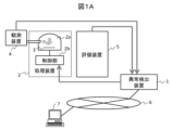
- FIG. 1 is a system configuration diagram of an anomaly detection system.
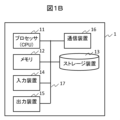
- FIG. 2 is a hardware configuration diagram of the abnormality detection device.
- FIG. 2 is a diagram showing data and programs stored in a storage device.
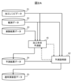
- FIG. 2 is a functional block diagram of the anomaly detection device in a learning (training) process.
- FIG. 4 is a functional block diagram of an abnormality detection device in an abnormality detection process. 4 is an example of a data structure of processing recipe data.
- 1 is an example of a data structure of observation data.
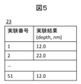
- 13 is an example of a data structure of experiment result data.
- 13 is an example of a data structure of prediction result data.
- 13 is an example of a data structure of normal contribution data.
- 1 is an overall flowchart of anomaly detection.
- 13 is a flow chart showing a calculation flow of a shape anomaly score of verification data. 13 is a flow chart showing a calculation flow of the contribution anomaly score of the verification data. 1 is an example of a data structure of knowledge data. 1 is an example of a GUI.
- Figure 1A shows a system configuration diagram of the anomaly detection system. Below, we will explain an example of using this system in process development for semiconductors or semiconductor devices that contain semiconductors. In process development, appropriate processing conditions are derived for semiconductor processing equipment that processes semiconductor samples to achieve a target, for example, a desired processed shape.
- the processing device 2 is a device that processes semiconductor samples.
- the type of processing performed by the processing device 2 is not limited.
- it includes a lithography device, a film formation device, a pattern processing device, an ion implantation device, and a cleaning device.
- the lithography device includes an exposure device, an electron beam drawing device, and an X-ray drawing device.
- the film formation device includes a CVD (Chemical Vapor Deposition), a PVD (Physical Vapor Deposition), an evaporation device, a sputtering device, and a thermal oxidation device.
- the pattern processing device includes a wet etching device, a dry etching device, an electron beam processing device, and a laser processing device.
- the ion implantation device includes a plasma doping device and an ion beam doping device.
- the cleaning device includes a liquid cleaning device and an ultrasonic cleaning device.
- the processing device 2 will be described as an example of a plasma processing device that performs etching processing of semiconductor samples.
- a high-frequency alternating electromagnetic field is applied to a processing gas in the reactor 2a to generate plasma, which is then used to etch the sample 3.
- the etching process in the reactor 2a is controlled according to a processing recipe set in the control unit 2b.
- the evaluation device 5 is a device that evaluates the processing performed by the processing device 2 on the sample 3. For example, it is a processing dimension measurement device that uses an electron microscope, and measures the processing dimensions of the sample 3 performed by the processing device 2.
- the observation device 4 is a device that observes the phenomena occurring in the reactor 2a while the processing device 2 is processing the sample 3. There are no limitations on the phenomenon to be observed, and it can be appropriately selected depending on the phenomenon acting on the sample 3 during processing by the processing device 2. Here, an example is described in which a spectrophotometer that observes the light emission of plasma in the reactor 2a is used as the observation device 4.
- the control unit 2b of the processing device 2 processes the sample 3 (here, etching process) according to the processing recipe data.
- the observation device 4 observes the light emission state of the plasma in the reactor 2a during the processing period of the processing device 2 and acquires observation data.
- the evaluation device 5 measures the processing dimensions of the sample 3 and acquires experimental result data.
- the processing recipe data and the acquired observation data and experimental result data are accessible from the anomaly detection device 1, and are used to create a processing result prediction model that predicts the processing results by the processing device, and to detect and determine abnormalities in the processing results, which will be described later.
- the user accesses the anomaly detection device 1 from a terminal 7 via the network 6 or directly from the input/output device of the anomaly detection device 1, and executes the anomaly detection process.
- the storage device 13 is typically composed of a HDD (Hard Disk Drive) or SSD (Solid State Drive) and stores the programs executed by the anomaly detection device 1, the data to be processed by the programs, or the data resulting from processing by the programs.
- the memory 12 is composed of RAM (Random Access Memory) and temporarily stores programs and data required to execute the programs in response to instructions from the processor 11.
- the processor 11 functions as a functional unit (functional block) that provides specified functions by executing programs loaded from the storage device 13 to the memory 12.
- the shape anomaly score display unit 63 displays the processing result of step S04 (see FIG. 8), the contribution anomaly score display unit 64 displays the processing result of step S05, the integrated judgment display unit 65 displays the processing result of step S06, and the knowledge display unit 66 displays the knowledge extracted in step S07.
Landscapes
- Engineering & Computer Science (AREA)
- Theoretical Computer Science (AREA)
- General Engineering & Computer Science (AREA)
- Physics & Mathematics (AREA)
- General Physics & Mathematics (AREA)
- Software Systems (AREA)
- Data Mining & Analysis (AREA)
- Computing Systems (AREA)
- Evolutionary Computation (AREA)
- Mathematical Physics (AREA)
- Artificial Intelligence (AREA)
- Automation & Control Theory (AREA)
- Computational Linguistics (AREA)
- Computer Vision & Pattern Recognition (AREA)
- Medical Informatics (AREA)
- Manufacturing & Machinery (AREA)
- Quality & Reliability (AREA)
- Drying Of Semiconductors (AREA)
- Testing And Monitoring For Control Systems (AREA)
Priority Applications (6)
| Application Number | Priority Date | Filing Date | Title |
|---|---|---|---|
| PCT/JP2023/006212 WO2024176347A1 (ja) | 2023-02-21 | 2023-02-21 | 異常検出装置及び異常検出方法 |
| US18/691,713 US20250364334A1 (en) | 2023-02-21 | 2023-02-21 | Abnormality detection apparatus and abnormality detection method |
| JP2024503336A JP7625133B2 (ja) | 2023-02-21 | 2023-02-21 | 異常検出装置及び異常検出方法 |
| KR1020247002380A KR20240131986A (ko) | 2023-02-21 | 2023-02-21 | 이상 검출 장치 및 이상 검출 방법 |
| CN202380013027.1A CN118830054A (zh) | 2023-02-21 | 2023-02-21 | 异常检测装置以及异常检测方法 |
| TW113103436A TWI895961B (zh) | 2023-02-21 | 2024-01-30 | 異常檢測裝置及異常檢測方法 |
Applications Claiming Priority (1)
| Application Number | Priority Date | Filing Date | Title |
|---|---|---|---|
| PCT/JP2023/006212 WO2024176347A1 (ja) | 2023-02-21 | 2023-02-21 | 異常検出装置及び異常検出方法 |
Publications (1)
| Publication Number | Publication Date |
|---|---|
| WO2024176347A1 true WO2024176347A1 (ja) | 2024-08-29 |
Family
ID=92500381
Family Applications (1)
| Application Number | Title | Priority Date | Filing Date |
|---|---|---|---|
| PCT/JP2023/006212 Ceased WO2024176347A1 (ja) | 2023-02-21 | 2023-02-21 | 異常検出装置及び異常検出方法 |
Country Status (6)
| Country | Link |
|---|---|
| US (1) | US20250364334A1 (https=) |
| JP (1) | JP7625133B2 (https=) |
| KR (1) | KR20240131986A (https=) |
| CN (1) | CN118830054A (https=) |
| TW (1) | TWI895961B (https=) |
| WO (1) | WO2024176347A1 (https=) |
Citations (6)
| Publication number | Priority date | Publication date | Assignee | Title |
|---|---|---|---|---|
| JP2005051269A (ja) * | 2004-10-12 | 2005-02-24 | Hitachi Ltd | 半導体処理装置 |
| JP2009054843A (ja) * | 2007-08-28 | 2009-03-12 | Omron Corp | プロセス異常検出装置および方法並びにプログラム |
| JP2020181959A (ja) * | 2019-04-26 | 2020-11-05 | 東京エレクトロン株式会社 | 学習方法、管理装置および管理プログラム |
| JP2021002295A (ja) * | 2019-06-24 | 2021-01-07 | 東京エレクトロンデバイス株式会社 | 異常検知装置、異常検知システム、及び異常検知方法 |
| JP2021086571A (ja) * | 2019-11-29 | 2021-06-03 | 東京エレクトロン株式会社 | 異常検知装置、異常検知方法及び異常検知プログラム |
| JP2023010604A (ja) * | 2021-07-08 | 2023-01-20 | 株式会社日立ハイテク | プロセスレシピ探索装置、エッチングレシピ探索方法及び半導体装置製造システム |
Family Cites Families (6)
| Publication number | Priority date | Publication date | Assignee | Title |
|---|---|---|---|---|
| JP5363213B2 (ja) * | 2009-06-30 | 2013-12-11 | 東京エレクトロン株式会社 | 異常検出システム、異常検出方法、記憶媒体及び基板処理装置 |
| US8406912B2 (en) * | 2010-06-25 | 2013-03-26 | Taiwan Semiconductor Manufacturing Company, Ltd. | System and method for data mining and feature tracking for fab-wide prediction and control |
| JP6824121B2 (ja) * | 2017-07-14 | 2021-02-03 | 株式会社東芝 | 状態検知装置、状態検知方法及びプログラム |
| JP6778666B2 (ja) | 2017-08-24 | 2020-11-04 | 株式会社日立製作所 | 探索装置及び探索方法 |
| KR102648654B1 (ko) * | 2020-06-15 | 2024-03-19 | 주식회사 히타치하이테크 | 장치 진단 장치, 장치 진단 방법, 플라스마 처리 장치 및 반도체 장치 제조 시스템 |
| CN114819242B (zh) * | 2021-01-28 | 2025-05-09 | 联华电子股份有限公司 | 考虑整体特征与局部特征的半导体工艺预测方法与装置 |
-
2023
- 2023-02-21 KR KR1020247002380A patent/KR20240131986A/ko active Pending
- 2023-02-21 WO PCT/JP2023/006212 patent/WO2024176347A1/ja not_active Ceased
- 2023-02-21 CN CN202380013027.1A patent/CN118830054A/zh active Pending
- 2023-02-21 US US18/691,713 patent/US20250364334A1/en active Pending
- 2023-02-21 JP JP2024503336A patent/JP7625133B2/ja active Active
-
2024
- 2024-01-30 TW TW113103436A patent/TWI895961B/zh active
Patent Citations (6)
| Publication number | Priority date | Publication date | Assignee | Title |
|---|---|---|---|---|
| JP2005051269A (ja) * | 2004-10-12 | 2005-02-24 | Hitachi Ltd | 半導体処理装置 |
| JP2009054843A (ja) * | 2007-08-28 | 2009-03-12 | Omron Corp | プロセス異常検出装置および方法並びにプログラム |
| JP2020181959A (ja) * | 2019-04-26 | 2020-11-05 | 東京エレクトロン株式会社 | 学習方法、管理装置および管理プログラム |
| JP2021002295A (ja) * | 2019-06-24 | 2021-01-07 | 東京エレクトロンデバイス株式会社 | 異常検知装置、異常検知システム、及び異常検知方法 |
| JP2021086571A (ja) * | 2019-11-29 | 2021-06-03 | 東京エレクトロン株式会社 | 異常検知装置、異常検知方法及び異常検知プログラム |
| JP2023010604A (ja) * | 2021-07-08 | 2023-01-20 | 株式会社日立ハイテク | プロセスレシピ探索装置、エッチングレシピ探索方法及び半導体装置製造システム |
Also Published As
| Publication number | Publication date |
|---|---|
| CN118830054A (zh) | 2024-10-22 |
| KR20240131986A (ko) | 2024-09-02 |
| JPWO2024176347A1 (https=) | 2024-08-29 |
| TWI895961B (zh) | 2025-09-01 |
| TW202435111A (zh) | 2024-09-01 |
| JP7625133B2 (ja) | 2025-01-31 |
| US20250364334A1 (en) | 2025-11-27 |
Similar Documents
| Publication | Publication Date | Title |
|---|---|---|
| US10627788B2 (en) | Retrieval apparatus and retrieval method for semiconductor device processing | |
| TWI745723B (zh) | 探索裝置 | |
| TWI830165B (zh) | 大批量製造半導體製程控制度量系統 | |
| KR100768017B1 (ko) | 툴 고장 모니터링을 위한 고장검출 및 가상 센서 방법 | |
| JP2011513993A (ja) | プロセスデータおよび生産量データを使用するプロセス制御 | |
| KR102206347B1 (ko) | 시스템 및 처리 조건의 결정 방법 | |
| KR20180074574A (ko) | 프로세스의 엔드포인트 제어를 위한 시계열 스펙트럼으로부터 특징 추출 방법 | |
| US20240047248A1 (en) | Adaptive model training for process control of semiconductor manufacturing equipment | |
| JP7424909B2 (ja) | 処理条件探索装置および処理条件探索方法 | |
| JP7808302B2 (ja) | 測定値違反解析を使用したプロセス異常の識別 | |
| JP7625133B2 (ja) | 異常検出装置及び異常検出方法 | |
| TWI734390B (zh) | 自資料集中提取特徵 | |
| Chen et al. | Optimizing etching process recipe based on kernel ridge regression | |
| JP2018014403A (ja) | プラズマ処理装置及びプラズマ処理データを解析する解析方法 | |
| US20250077885A1 (en) | Search apparatus, search method, and semiconductor device manufacturing system | |
| JP7710965B2 (ja) | 情報処理装置、情報処理方法およびプログラム | |
| Naeini et al. | A bayesian approach for recognition of control chart patterns | |
| JP2023544502A (ja) | 可解釈な深層学習ベース欠陥検出及び分類 | |
| JP2020025116A (ja) | 探索装置および探索方法 | |
| TW202601752A (zh) | 電腦程式、資訊處理方法及資訊處理裝置 | |
| KR20240078771A (ko) | Euv 설비 상태 진단 장치 및 방법 | |
| JP2024148034A (ja) | 異常診断装置、異常診断方法及び異常診断プログラム |
Legal Events
| Date | Code | Title | Description |
|---|---|---|---|
| WWE | Wipo information: entry into national phase |
Ref document number: 2024503336 Country of ref document: JP |
|
| WWE | Wipo information: entry into national phase |
Ref document number: 202380013027.1 Country of ref document: CN |
|
| WWE | Wipo information: entry into national phase |
Ref document number: 18691713 Country of ref document: US |
|
| 121 | Ep: the epo has been informed by wipo that ep was designated in this application |
Ref document number: 23924001 Country of ref document: EP Kind code of ref document: A1 |
|
| NENP | Non-entry into the national phase |
Ref country code: DE |
|
| WWP | Wipo information: published in national office |
Ref document number: 18691713 Country of ref document: US |
|
| 122 | Ep: pct application non-entry in european phase |
Ref document number: 23924001 Country of ref document: EP Kind code of ref document: A1 |