WO2024176329A1 - 誤り訂正回路、制御装置、及び方法 - Google Patents
誤り訂正回路、制御装置、及び方法 Download PDFInfo
- Publication number
- WO2024176329A1 WO2024176329A1 PCT/JP2023/006153 JP2023006153W WO2024176329A1 WO 2024176329 A1 WO2024176329 A1 WO 2024176329A1 JP 2023006153 W JP2023006153 W JP 2023006153W WO 2024176329 A1 WO2024176329 A1 WO 2024176329A1
- Authority
- WO
- WIPO (PCT)
- Prior art keywords
- circuit
- data
- error correction
- decoding
- setting unit
- Prior art date
- Legal status (The legal status is an assumption and is not a legal conclusion. Google has not performed a legal analysis and makes no representation as to the accuracy of the status listed.)
- Ceased
Links
Images



Classifications
-
- G—PHYSICS
- G06—COMPUTING OR CALCULATING; COUNTING
- G06F—ELECTRIC DIGITAL DATA PROCESSING
- G06F11/00—Error detection; Error correction; Monitoring
- G06F11/07—Responding to the occurrence of a fault, e.g. fault tolerance
- G06F11/08—Error detection or correction by redundancy in data representation, e.g. by using checking codes
- G06F11/10—Adding special bits or symbols to the coded information, e.g. parity check, casting out 9's or 11's
Definitions
- This disclosure relates to an error correction circuit, a control device, and a method.
- Many industrial machines are installed at manufacturing sites such as factories.
- the control devices of the industrial machines are connected to various computers such as management devices and production planning devices via a network, and operate while communicating with each other.
- various industrial machines and peripheral devices are in operation, and noise generated from these can cause data corruption due to bit inversion during data transmission during communication.
- noise can cause data corruption in memory such as RAM, HDD, and SSD.
- raw data is not handled as is, but rather the data is encoded to make it redundant and to enable error detection and correction (for example, see Patent Document 1).
- data encoding can also be used to encrypt communications. The encoded data is decoded when it is used.
- Encoding algorithms vary in terms of encoding and decoding speed, redundancy, etc. depending on the type and how they are used. In the field, there is a demand to use the most suitable encoding algorithm depending on the device status.
- the error correction circuit disclosed herein solves the above problem by determining the state of a device, such as how it is broken, based on error trends and switching the encoding algorithm.
- An aspect of the present disclosure is an error correction circuit comprising a plurality of devices, a controller for writing and reading data to the devices, an encoding circuit for encoding data to be written to the devices, a decoding circuit capable of changing logic circuits for decoding data read from the devices, an inspection circuit for detecting errors in the data read from the devices, and a setting unit for reconfiguring the decoding circuit, in which redundant data is added to the data read from the devices, the inspection circuit detects data errors using the redundant data added to the data read from the devices, and the setting unit reconfigures the decoding circuit to a logic circuit that performs decoding appropriate to the failure status of the devices when it is determined that the devices are faulty based on the tendency of errors detected by the inspection circuit.
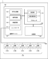
- FIG. 1 is a schematic configuration diagram of an error correction circuit according to a first embodiment of the present disclosure.
- 1 is a block diagram showing a schematic function of an error correction circuit according to a first embodiment of the present disclosure used as a memory controller.
- FIG. 11 is a schematic configuration diagram of a modified example of the error correction circuit according to the first embodiment of the present disclosure.
- FIG. 11 is a schematic configuration diagram of an error correction circuit according to a second embodiment of the present disclosure.
- FIG. 13 is a schematic configuration diagram of an error correction circuit according to a third embodiment of the present disclosure.
- FIG. 13 is a screen configuration diagram showing an example of a screen for notifying a user of a device failure according to the third embodiment.
- FIG. 13 is a schematic configuration diagram of an error correction circuit according to another embodiment of the present disclosure.
- FIG. 1 is a block diagram showing a schematic configuration of an error correction circuit 100 according to a first embodiment of the present disclosure.
- the error correction circuit 100 according to this embodiment can be incorporated into a memory read/write section and a communication circuit transmission/reception section in a control device 1 that controls industrial machines such as machine tools and robots.
- the error correction circuit 100 can be configured as a device that writes and reads data to and from multiple devices.
- Examples of multiple devices include storage devices such as ROM (Read Only Memory), RAM (Random Access Memory), HDD (Hard Disk Drive), and SSD (Solid State Drive), external storage devices that exchange data with external storage such as USB memory and SD card, and communication devices for communicating data with other devices located remotely.
- storage devices such as ROM (Read Only Memory), RAM (Random Access Memory), HDD (Hard Disk Drive), and SSD (Solid State Drive), external storage devices that exchange data with external storage such as USB memory and SD card, and communication devices for communicating data with other devices located remotely.
- the error correction circuit 100 of this embodiment is configured with a processor 110, a memory unit 120, and a logical device 130 connected via a bus 180.
- the processor 110 is, for example, a CPU (Central Processing Unit).
- a trend analysis unit 111 which functions as a hardware circuit or by executing specific system software, and a setting unit 112 are configured on the processor 110.
- the storage unit 120 is, for example, a ROM, RAM, HDD, SSD, etc.
- the logic device 130 is, for example, an LSI (Large Scale Integration).
- a controller 131, an encoding circuit 132, a plurality of decoding circuits 133, and an inspection circuit 134 are configured on the logic device 130.
- the controller 131 writes and reads data to the devices. Based on instructions from the processor 110, the controller 131 writes specific data to multiple devices. Based on instructions from the processor 110, the controller 131 also reads specific data from multiple devices and passes it to the processor 110. When writing data to each device, the controller 131 uses the encoding circuit 132 to encode the data. Also, for each device, the controller 131 adds specific redundant data to the data written to the device. The redundant data may be well-known data such as a parity bit or CRC. When reading data from each device, the controller 131 decodes the data using a decoding circuit 133 that is set according to the state of the device.
- the encoding circuit 132 is a circuit that encodes data to be written to the device.
- the encoding circuit 132 is constructed using a logic circuit to implement a specific encoding algorithm.
- the encoding circuit 132 encodes data to be written to the device based on the specific encoding algorithm.
- the decoding circuit 133 is a circuit that decodes data read from the device.
- the decoding circuits 133 are constructed with logic circuits that implement different predetermined decoding algorithms.
- the decoding algorithm of the decoding circuit 133 is for decoding data that has been coded by the coding algorithm of the coding circuit 132.
- the inspection circuit 134 inspects the data read by the controller 131 and detects errors such as corruption of the data. Redundant data such as parity and CRC is added to the data read from each device. The inspection circuit 134 detects data errors by inspecting the data using this redundant data. If the inspection circuit 134 detects an error in the data read from a device, it outputs information related to the read data (e.g., information identifying the device that read the data, the address of the read data within the device, etc.) to the trend analysis unit 111.
- information related to the read data e.g., information identifying the device that read the data, the address of the read data within the device, etc.
- the trend analysis unit 111 analyzes the tendency of errors in data read from a device detected by the inspection circuit 134. If it is determined from the analyzed tendency of errors that some kind of failure has occurred in a specific device, it instructs the setting unit 112 to use the decoding circuit 133 according to the tendency of errors. For example, the trend analysis unit 111 may determine that some kind of failure has occurred in the device when an error has occurred in data read from the specific device a predetermined number of times or more in succession, or when an error has occurred in data read from the specific device at a predetermined frequency in the most recent predetermined number of data reads. The trend analysis unit 111 may analyze the device state in more detail. For example, if there is a tendency for errors to occur frequently only at a specific address in the data read from the device, it may determine that a failure has occurred at that address in the device.
- the setting unit 112 selects a decoding circuit 133 suitable for the error occurrence tendency of the data read from the device analyzed by the trend analysis unit 111. Then, it sets the controller 131 to use the selected decoding circuit 133.
- the decoding circuit 133 selected by the setting unit 112 may be for configuring a circuit that decodes data by excluding data of a device determined to have some kind of failure based on the error occurrence tendency. Furthermore, when the setting unit 112 is notified of a more detailed error occurrence tendency from the trend analysis unit 111, it may set the parameters of the selected decoding circuit 133 to match the detailed error occurrence tendency. For example, when the device failure is limited to a specific address, it may set the decoding circuit 133 to partially change the decoding algorithm according to the range of the failed address.
- FIG. 2 is a block diagram showing a schematic configuration of the error correction circuit 100 according to this embodiment used as a memory controller.
- the storage device 210 is, for example, a RAM.
- the storage device 210 is composed of multiple storage devices 210A to 210E.
- the storage device 210 is connected to the logical device 130 via a memory bus 200.
- the controller 131 writes data to the storage device 210 and reads data from the storage device 210 via the memory bus 200.
- the encoding circuit 132 when the controller 131 writes data to the storage devices 210, the encoding circuit 132 encodes the data using a known error correction encoding algorithm such as turbo code, LDCP code, or Reed-Solomon code. The encoding circuit 132 may also use a unique error correction encoding algorithm. The controller 131 then writes the encoded data to each of the storage devices 210A-210E. When writing data, the controller 131 adds redundant data to the data for each device.
- a known error correction encoding algorithm such as turbo code, LDCP code, or Reed-Solomon code.
- the controller 131 then writes the encoded data to each of the storage devices 210A-210E.
- the controller 131 adds redundant data to the data for each device.
- the controller 131 When the controller 131 reads data from the storage device 210, the data read from each of the storage devices 210A to 210E is decoded by the decoding circuit 133 set according to the current state of the storage device.
- the inspection circuit 134 When the controller 131 reads data from the storage device 210, the inspection circuit 134 performs an inspection using redundant data on the data read from each device. The inspection result is sent to the setting unit 112. Here, for example, in the most recent predetermined number of data reads, an error is detected at a predetermined frequency in the data read from the storage device 210C.
- the setting unit 112 selects the decoding circuit 133 for decoding data based on the data read from the storage devices 210A, 210B, 210D, and 210E, assuming that the data read from the storage device 210C is an error.
- the selected decoding circuit 133 is then used to decode the read data. From this point on, the decoding circuit 133 that performs the decoding process without using the data from the storage device 210C is used.
- redundant data is added to the data read from each device.
- This redundant data is used to analyze the state of the device to determine whether it is operating normally or has failed. If it is determined from the analysis results that the device is faulty, the circuit is logically switched to the decoding circuit 133 which executes the most suitable decoding algorithm. Since hardware is used for data encoding and decoding, data can be encoded and decoded at high speed. In addition, since the decoding algorithm can be changed according to the device status, processing can be made flexible. This makes it possible to use a decoding algorithm that assumes that data read from a faulty device contains an error, thereby improving the speed and accuracy of decoding.
- the error correction circuit 100 can be incorporated into the memory read/write and communication circuit transmission/reception parts of a control device 1 that controls industrial machines such as machine tools and robots.
- Data written to devices such as memory and communication circuits can cause errors due to, for example, the effects of cosmic rays, failure of the device itself, solder cracks, noise, and other mechanical factors. The above factors can also cause partial damage to the device itself. In such situations, the error correction circuit 100 according to this embodiment is expected to operate appropriately.
- the trend analysis unit 111 that analyzes the trend of error occurrence may be configured as a specified logic circuit on the logic device 130, rather than being configured on the processor 110.
- the occurrence of errors in each device detected by the inspection circuit 134 is statistically recorded on the logic circuit, and the trend of error occurrence is analyzed from the statistical record. Then, when a predetermined trend is observed, a command is output to the setting unit 112 to select an appropriate decoding circuit 133.
- the setting unit 112 switches between the encoding circuit 132, the decoding circuit 133, and the inspection circuit 134 according to the tendency of errors in the data read from the device analyzed by the tendency analysis unit 111. Since it is difficult to switch the encoding circuit 132 or the inspection circuit 134 while the control device 1 is in operation, if switching of the encoding circuit 132 or the inspection circuit 134 is selected during operation, this is stored in a predetermined area of the storage unit 120.
- multiple tendency analysis units 111 may be configured as logical circuits on the logical device 130. In this case, it is also possible to select an appropriate tendency analysis unit 111 according to the state of the device according to the tendency of errors in the data read from the device. This configuration allows the encoding and decoding algorithms to be changed more flexibly to suit the device's status, making processing more flexible.
- [Second embodiment] 4 is a block diagram showing a schematic configuration of an error correction circuit 100 according to a second embodiment of the present disclosure.
- the error correction circuit 100 according to this embodiment differs from the error correction circuit 100 according to the first embodiment in that the logic device 130 is configured as a reconfigurable device.
- the processor 110 is, for example, a CPU.
- a trend analysis unit 111 which functions as a hardware circuit or by executing specific system software, and a setting unit 112 are configured on the processor 110.
- the storage unit 120 is, for example, a ROM, RAM, HDD, SSD, etc.
- the storage unit 120 stores in advance a plurality of configuration files 121 for configuring a logic circuit on the logic device 130.
- the logic device 130 is, for example, an FPGA (Field Programmable Gate Array).
- a controller 131, an encoding circuit 132, a decoding circuit 133, and an inspection circuit 134 are configured on the logic device 130.
- the controller 131 writes and reads data to the devices. Based on instructions from the processor 110, the controller 131 writes specific data to multiple devices. Based on instructions from the processor 110, the controller 131 also reads specific data from multiple devices and passes it to the processor 110. When writing data to each device, the controller 131 uses the encoding circuit 132 to encode the data. Also, for each device, the controller 131 adds specific redundant data to the data written to the device. The redundant data may be well-known data such as a parity bit or CRC. When reading data from each device, the controller 131 decodes the data using the decoding circuit 133.
- the encoding circuit 132 is a circuit that encodes data to be written to the device.
- the encoding circuit 132 encodes the data to be written to the device based on a predetermined encoding algorithm.
- the decoding circuit 133 is a circuit that decodes data read from the device.
- the decoding circuit 133 is configured by reconfiguring the logical device 130 based on the configuration file 121 stored in the storage unit 120.
- the decoding algorithm of the decoding circuit 133 is for decoding data that has been encoded by the encoding algorithm of the encoding circuit 132.
- the inspection circuit 134 inspects the data read by the controller 131 and detects errors such as corruption of the data. Redundant data such as parity and CRC is added to the data read from each device. The inspection circuit 134 detects data errors by inspecting the data using this redundant data. If the inspection circuit 134 detects an error in the data read from a device, it outputs information related to the read data (e.g., information identifying the device that read the data, the address of the read data within the device, etc.) to the trend analysis unit 111.
- information related to the read data e.g., information identifying the device that read the data, the address of the read data within the device, etc.
- the trend analysis unit 111 analyzes the tendency of errors in data read from a device detected by the inspection circuit 134. If it is determined from the analyzed tendency of errors that some kind of failure has occurred in a specific device, it instructs the setting unit 112 to reconfigure the decoding circuit 133 according to the tendency of errors. For example, the trend analysis unit 111 may determine that some kind of failure has occurred in the device when an error has occurred in data read from the specific device a predetermined number of times or more in succession, or when an error has occurred in data read from the specific device at a predetermined frequency in the most recent predetermined number of data reads. The trend analysis unit 111 may analyze the device state in more detail. For example, if there is a tendency for errors to occur frequently only at a specific address in the data read from the device, it may determine that a failure has occurred at that address in the device.
- the setting unit 112 selects a configuration file 121 suitable for the tendency of errors occurring in the data read from the device analyzed by the trend analysis unit 111.
- the selected configuration file 121 is then used to reconfigure the circuit configuration of the decoding circuit 133.
- the configuration file 121 selected by the setting unit 112 may be for configuring a circuit that decodes data by excluding data from a device that has been determined to have some kind of failure based on the tendency of errors occurring.
- the setting unit 112 may set parameters of the selected configuration file 121 to match the detailed tendency of errors occurring. For example, when the device failure is limited to a specific address, the parameters of the configuration file 121 may be set to partially change the decoding algorithm according to the range of the failed addresses.
- redundant data is added to the data read from each device.
- This redundant data is used to analyze the state of the device to determine whether it is operating normally or has failed. If it is determined from the analysis result that the device is faulty, the decoding circuit 133 is reconfigured to switch the decoding algorithm to an optimal one. In this way, since reconfigurable hardware is used for encoding and decoding data, data can be encoded and decoded at high speed. In addition, since the decoding algorithm can be changed according to the device status, processing can be made flexible. This makes it possible to use a decoding algorithm that assumes that data read from a faulty device is an error, thereby improving the decoding speed and accuracy.
- the necessary circuits can be implemented on the logic device 130 at any timing according to the device status. Therefore, there is no need to physically create various circuits to cover all the expected encoding and decoding patterns, and the circuit scale is reduced, and it is possible to achieve power saving by eliminating the need to operate multiple algorithm circuits simultaneously.
- the trend analysis unit 111 that analyzes the trend of error occurrence may be configured as a specified logic circuit on the logic device 130, rather than being configured on the processor 110.
- the occurrence of errors in each device detected by the inspection circuit 134 is statistically recorded on the logic circuit, and the trend of error occurrence is analyzed from the statistical record. Then, when a predetermined trend is observed, a command is output to the setting unit 112 to reconfigure the decoding circuit 133.
- the configuration file 121 may reconfigure not only the decoding circuit 133 but also the encoding circuit 132 and the inspection circuit 134.
- the setting unit 112 reconfigures the encoding circuit 132, the decoding circuit 133, and the inspection circuit 134 according to the tendency of errors in the data read from the device analyzed by the tendency analysis unit 111. Since it is difficult to reconfigure the encoding circuit 132 and the inspection circuit 134 while the control device 1 is in operation, when it is selected to reconfigure the encoding circuit 132 and the inspection circuit 134 during operation, this is stored in a specified area of the storage unit 120.
- the respective circuits may be reconfigured with the selected configuration file 121 the next time the control device 1 is started.
- the tendency analysis unit 111 may be further reconfigured according to the tendency of errors in the data read from the device. This configuration allows the encoding and decoding algorithms to be changed more flexibly to suit the device's status, making processing more flexible.
- FIG. 5 is a block diagram showing a schematic configuration of an error correction circuit 100 according to a third embodiment of the present disclosure.
- the error correction circuit 100 according to this embodiment further includes a notification unit 113 in addition to the components of the error correction circuit 100 according to the first embodiment.
- the trend analysis unit 111 in this embodiment determines that some kind of failure has occurred in a specific device, it instructs the setting unit 112 to reconfigure the decoding circuit 133 and also instructs the notification unit 113 to notify the failure state of the device.
- the notification unit 113 When the notification unit 113 is instructed to notify the failure state of a device, it notifies the user that the device has failed.
- the notification unit 113 may display, for example, on a display device (not shown) information that identifies the device, along with information indicating that the device has failed. At that time, an alarm may be sounded.
- the device failure may also be notified by a lamp or the like provided on an operation panel or the like.
- Figure 6 shows an example of a screen configuration displayed on a display device by the notification unit 113 to notify the user of a device failure. In the example of Figure 6, a message is displayed encouraging the user to replace the expansion board on which the failed device is mounted.
- the trend analysis unit 111 may also instruct the unit to run a program that reads out data stored in the device and backs it up in an external storage device (not shown). If data such as machining programs and parameters are stored in the device, automatically backing up this data will make it easier to replace the device later.
- the error correction circuit 100 which has the above configuration, makes it possible to quickly start work on the device when a device failure is detected.
- FIG. 7 is a block diagram showing a schematic configuration of the error correction circuit 100 according to another embodiment of the present disclosure.
- the functions corresponding to the controller 131, the encoding circuit 132, the decoding circuit 133, and the inspection circuit 134 constructed on the logical device 130 by the error correction circuit 100 according to the second embodiment are constructed in software on the processor 110 as a controller unit 114, an encoding unit 115, a decoding unit 116, and an inspection unit 117, respectively.
- the storage unit 120 stores in advance a program 122 for realizing each function.
- the error correction circuit 100 configured in this way can implement the necessary functions on the processor 110 at any time depending on the device's situation. Therefore, there is no need to physically create various circuits to cover all possible encoding and decoding patterns, which reduces the circuit scale and makes it possible to save power by eliminating the need to operate multiple algorithm circuits simultaneously.
- the error correction circuit 100 is capable of changing the encoding algorithm and decoding algorithm in response to the device conditions, which allows for flexibility in processing.
- An error correction circuit (100) includes a plurality of devices (210), a controller (131) that writes and reads data to the devices (210), an encoding circuit (132) that encodes data to be written to the devices (210), a decoding circuit (133) that can change logic circuits and decodes data read from the devices (210), an inspection circuit (134) that detects errors in the data read from the devices (210), and a controller that switches between the decoding circuits (133).
- the encoding circuit (132) is capable of changing the logic circuit, and when the setting unit (112) determines that the device (210) is faulty based on the error occurrence tendency detected by the inspection circuit (134), it further switches the encoding circuit (132) to a logic circuit that performs encoding appropriate to the fault condition of the device (210).
- the inspection circuit (134) is capable of changing the logic circuit, and when the setting unit (112) determines that the device (210) is faulty based on the tendency of errors detected by the inspection circuit (134), it further switches the inspection circuit (134) to a logic circuit that performs inspection appropriate to the fault condition of the device (210).
- An error correction circuit (100) according to another aspect of the present disclosure further includes a trend analysis unit (111) for analyzing the tendency of errors to occur in the read data, and the setting unit (112) selects a destination logic circuit based on the tendency of errors to occur analyzed by the trend analysis unit (111).
- the trend analysis unit (111) is configured with a reconfigurable logic circuit, and when the setting unit (112) determines that the device (210) is faulty based on the error occurrence tendency detected by the inspection circuit (134), it switches the trend analysis unit (111) to a logic circuit that performs trend analysis appropriate to the failure status of the device (210).
- the setting unit (112) sets parameters in the decoding circuit (133) according to the tendency of errors to occur.
- An error correction circuit (100) further includes a memory unit (120) in which a plurality of configuration files (121) are stored, and the setting unit (112) selects a configuration file (121) from the memory unit (120) for reconfiguring the logic circuit to a state suitable for the failure condition of the device (210), and switches by reconfiguring the logic circuit based on the selected configuration file (121).
- the error correction circuit (100) according to another aspect of the present disclosure further includes a notification unit (113) that notifies a failure of the device (210) when it is determined that the device (210) has failed.
- an error correction circuit (100) reads data from the device (210) and backs it up when the device (210) is determined to have failed.
- a control device (1) for an industrial machine includes the error correction circuit.
- a method includes an error correction circuit that performs the following steps when reading encoded data from multiple devices: checking the encoded data for errors; analyzing the tendency of errors to occur in the read encoded data; and, if the analysis determines that any of the multiple devices is faulty, switching a decoding circuit that decodes the encoded data to a logic circuit that performs decoding appropriate to the failure status of the device.
Landscapes
- Engineering & Computer Science (AREA)
- Theoretical Computer Science (AREA)
- Quality & Reliability (AREA)
- Physics & Mathematics (AREA)
- General Engineering & Computer Science (AREA)
- General Physics & Mathematics (AREA)
- Detection And Correction Of Errors (AREA)
Priority Applications (2)
| Application Number | Priority Date | Filing Date | Title |
|---|---|---|---|
| JP2025501957A JPWO2024176329A1 (https=) | 2023-02-21 | 2023-02-21 | |
| PCT/JP2023/006153 WO2024176329A1 (ja) | 2023-02-21 | 2023-02-21 | 誤り訂正回路、制御装置、及び方法 |
Applications Claiming Priority (1)
| Application Number | Priority Date | Filing Date | Title |
|---|---|---|---|
| PCT/JP2023/006153 WO2024176329A1 (ja) | 2023-02-21 | 2023-02-21 | 誤り訂正回路、制御装置、及び方法 |
Publications (1)
| Publication Number | Publication Date |
|---|---|
| WO2024176329A1 true WO2024176329A1 (ja) | 2024-08-29 |
Family
ID=92500396
Family Applications (1)
| Application Number | Title | Priority Date | Filing Date |
|---|---|---|---|
| PCT/JP2023/006153 Ceased WO2024176329A1 (ja) | 2023-02-21 | 2023-02-21 | 誤り訂正回路、制御装置、及び方法 |
Country Status (2)
| Country | Link |
|---|---|
| JP (1) | JPWO2024176329A1 (https=) |
| WO (1) | WO2024176329A1 (https=) |
Citations (7)
| Publication number | Priority date | Publication date | Assignee | Title |
|---|---|---|---|---|
| JPH08320713A (ja) * | 1995-05-24 | 1996-12-03 | Fanuc Ltd | 数値制御装置 |
| JPH1125005A (ja) * | 1997-07-07 | 1999-01-29 | Fanuc Ltd | メモリ制御方法 |
| JP2005252622A (ja) * | 2004-03-03 | 2005-09-15 | Kitakyushu Foundation For The Advancement Of Industry Science & Technology | 通信装置及び通信方法 |
| JP2008191864A (ja) * | 2007-02-02 | 2008-08-21 | Toshiba Tec Corp | データ処理装置及びその起動方法 |
| JP2009519660A (ja) * | 2005-12-14 | 2009-05-14 | エヌエックスピー ビー ヴィ | 無線チャネルを介する通信方法およびrfidリーダ |
| JP2016161990A (ja) * | 2015-02-26 | 2016-09-05 | ファナック株式会社 | 誤り訂正機能による寿命予測を有する制御装置 |
| JP2019164762A (ja) * | 2018-03-19 | 2019-09-26 | ファナック株式会社 | 情報処理装置,機械学習装置及びシステム |
-
2023
- 2023-02-21 WO PCT/JP2023/006153 patent/WO2024176329A1/ja not_active Ceased
- 2023-02-21 JP JP2025501957A patent/JPWO2024176329A1/ja active Pending
Patent Citations (7)
| Publication number | Priority date | Publication date | Assignee | Title |
|---|---|---|---|---|
| JPH08320713A (ja) * | 1995-05-24 | 1996-12-03 | Fanuc Ltd | 数値制御装置 |
| JPH1125005A (ja) * | 1997-07-07 | 1999-01-29 | Fanuc Ltd | メモリ制御方法 |
| JP2005252622A (ja) * | 2004-03-03 | 2005-09-15 | Kitakyushu Foundation For The Advancement Of Industry Science & Technology | 通信装置及び通信方法 |
| JP2009519660A (ja) * | 2005-12-14 | 2009-05-14 | エヌエックスピー ビー ヴィ | 無線チャネルを介する通信方法およびrfidリーダ |
| JP2008191864A (ja) * | 2007-02-02 | 2008-08-21 | Toshiba Tec Corp | データ処理装置及びその起動方法 |
| JP2016161990A (ja) * | 2015-02-26 | 2016-09-05 | ファナック株式会社 | 誤り訂正機能による寿命予測を有する制御装置 |
| JP2019164762A (ja) * | 2018-03-19 | 2019-09-26 | ファナック株式会社 | 情報処理装置,機械学習装置及びシステム |
Also Published As
| Publication number | Publication date |
|---|---|
| JPWO2024176329A1 (https=) | 2024-08-29 |
Similar Documents
| Publication | Publication Date | Title |
|---|---|---|
| JP6880795B2 (ja) | 制御装置およびその制御方法 | |
| JP5014899B2 (ja) | 再構成可能デバイス | |
| US20040168101A1 (en) | Redundant memory system and memory controller used therefor | |
| JP2012113466A (ja) | メモリコントローラ及び情報処理システム | |
| JP2005234883A (ja) | 記憶装置のデータ書き込み、読み出し方法およびデータ記憶システム | |
| JP2010128773A (ja) | ディスクアレイ装置、そのディスク管理方法及びそのディスク管理プログラム | |
| JPS6235704B2 (https=) | ||
| JP4456552B2 (ja) | 動的代替機能を持つ論理集積回路、これを用いた情報処理装置及び論理集積回路の動的代替方法 | |
| JP7268554B2 (ja) | 制御装置および制御方法 | |
| US9230687B2 (en) | Implementing ECC redundancy using reconfigurable logic blocks | |
| CN120821605B (zh) | 故障检测系统、方法、电子设备、存储介质和程序产品 | |
| WO2024176329A1 (ja) | 誤り訂正回路、制御装置、及び方法 | |
| JP4387968B2 (ja) | 障害検出装置および障害検出方法 | |
| WO2015068285A1 (ja) | プログラマブルデバイス及びこれを用いた電子システム装置 | |
| JP5910356B2 (ja) | 電子装置、電子装置制御方法及び電子装置制御プログラム | |
| CN110990201A (zh) | 一种自愈管理控制器、SoC及自愈方法 | |
| JP6194496B2 (ja) | 情報処理装置、情報処理方法、及びプログラム | |
| KR100194979B1 (ko) | 이중화 프로세서 시스템의 동작모드 결정방법 | |
| JPS6256538B2 (https=) | ||
| JPH07134636A (ja) | ディスクアレイ装置 | |
| JP2009514064A (ja) | 半導体回路のコンフィギュレーション装置およびコンフィギュレーション方法 | |
| JP2006059002A (ja) | 記憶装置 | |
| JPWO2024176329A5 (https=) | ||
| JPH0922387A (ja) | メモリ装置 | |
| CN121301054A (zh) | 位流数据处理方法及可编程逻辑器件 |
Legal Events
| Date | Code | Title | Description |
|---|---|---|---|
| 121 | Ep: the epo has been informed by wipo that ep was designated in this application |
Ref document number: 23923983 Country of ref document: EP Kind code of ref document: A1 |
|
| WWE | Wipo information: entry into national phase |
Ref document number: 2025501957 Country of ref document: JP |
|
| NENP | Non-entry into the national phase |
Ref country code: DE |
|
| 122 | Ep: pct application non-entry in european phase |
Ref document number: 23923983 Country of ref document: EP Kind code of ref document: A1 |