WO2024171288A1 - 電子部品 - Google Patents
電子部品 Download PDFInfo
- Publication number
- WO2024171288A1 WO2024171288A1 PCT/JP2023/004955 JP2023004955W WO2024171288A1 WO 2024171288 A1 WO2024171288 A1 WO 2024171288A1 JP 2023004955 W JP2023004955 W JP 2023004955W WO 2024171288 A1 WO2024171288 A1 WO 2024171288A1
- Authority
- WO
- WIPO (PCT)
- Prior art keywords
- covering
- electronic component
- base
- protrusion
- protruding
- Prior art date
- Legal status (The legal status is an assumption and is not a legal conclusion. Google has not performed a legal analysis and makes no representation as to the accuracy of the status listed.)
- Ceased
Links
Images




Classifications
-
- H—ELECTRICITY
- H01—ELECTRIC ELEMENTS
- H01F—MAGNETS; INDUCTANCES; TRANSFORMERS; SELECTION OF MATERIALS FOR THEIR MAGNETIC PROPERTIES
- H01F27/00—Details of transformers or inductances, in general
- H01F27/06—Mounting, supporting or suspending transformers, reactors or choke coils not being of the signal type
-
- H—ELECTRICITY
- H01—ELECTRIC ELEMENTS
- H01F—MAGNETS; INDUCTANCES; TRANSFORMERS; SELECTION OF MATERIALS FOR THEIR MAGNETIC PROPERTIES
- H01F27/00—Details of transformers or inductances, in general
- H01F27/02—Casings
-
- H—ELECTRICITY
- H01—ELECTRIC ELEMENTS
- H01F—MAGNETS; INDUCTANCES; TRANSFORMERS; SELECTION OF MATERIALS FOR THEIR MAGNETIC PROPERTIES
- H01F27/00—Details of transformers or inductances, in general
- H01F27/28—Coils; Windings; Conductive connections
- H01F27/29—Terminals; Tapping arrangements for signal inductances
-
- H—ELECTRICITY
- H05—ELECTRIC TECHNIQUES NOT OTHERWISE PROVIDED FOR
- H05K—PRINTED CIRCUITS; CASINGS OR CONSTRUCTIONAL DETAILS OF ELECTRIC APPARATUS; MANUFACTURE OF ASSEMBLAGES OF ELECTRICAL COMPONENTS
- H05K5/00—Casings, cabinets or drawers for electric apparatus
Definitions
- the present invention relates to electronic components.
- Patent Document 1 describes a vehicle glass module (1) in which a terminal (glass-side conductor (7) in Patent Document 1) extends from a side surface of an end portion in the longitudinal direction of a base portion (main body (10) in Patent Document 1).
- stress is concentrated in a part of the base that surrounds the base end of the protruding terminal.
- stress may be concentrated in a corner that is the opening end of a recess in the base that is formed for embedding the terminal.
- Such stress concentration can cause problems such as the base being destroyed or the terminal being deformed.
- the present invention was made in consideration of the above-mentioned problems, and provides an electronic component in which damage to the base portion is prevented or deformation of the terminals is suppressed when an external force is applied to the electronic component.
- the electronic component of the present invention is an electronic component having a base portion with a housing portion for housing an electronic element, and a terminal that is partially embedded in the base portion and has one end protruding outward from the base portion, and is characterized in that the base portion has a covering portion that extends from the outer surface of the base portion and covers at least a portion of the periphery of the base end of the one end.
- the base end of one end of the protruding terminal is covered by a coating extending from the base, so that when an external force is applied to the electronic component, the stress on the base is distributed from the base end to the tip of the coating. This prevents damage to the base and deformation of the terminal when an external force is applied to the electronic component.
- the electronic component of the present invention can prevent damage to the base portion or suppress deformation of the terminals when an external force is applied to the electronic component.
- FIG. 1 is a perspective view showing an example of an electronic component according to a first embodiment of the present invention, in which the outer shape of a housing portion is shown by a dotted line.
- 1 is a perspective view of an electronic component according to a first embodiment, in which a case and a base are omitted, and only the outline of the base is indicated by a dotted line.
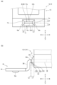
- 1 is a side view of an electronic component according to a first embodiment, in which the outer shape of a terminal embedded in a base portion, the shape of a plug connection portion, the shape of a pin, and the outer shape of a housing portion are illustrated by dotted lines.
- FIG. 1 is a front view of an electronic component according to a first embodiment.
- FIG. 2 is a rear view of the electronic component according to the first embodiment.
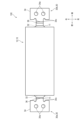
- FIG. 2 is a top view of the electronic component according to the first embodiment.
- FIG. 2 is a bottom view of the electronic component according to the first embodiment.
- Fig. 8(a) is an enlarged view of the covering portion and its vicinity in Fig. 4. However, the mounting portion and the standing portion, which are part of the terminal, are not shown.
- Fig. 8(b) is an enlarged view of the terminal and its vicinity in Fig. 3.
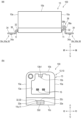
- 9A is a side view of an example of an electronic component according to a second embodiment of the present invention
- FIG 9B is a front view of the electronic component, in which a mounting portion and a standing portion that are part of a terminal are omitted.
- FIG. 10A is a side view of another example of an electronic component according to the second embodiment of the present invention
- FIG. 10B is a front view of the electronic component, in which a mounting portion and a standing portion that are part of a terminal are not shown.
- 11(a) is a diagram illustrating the results of calculating the stress applied to the control electronic component
- FIG. 11(b) is a diagram illustrating the results of calculating the stress applied to the electronic component.
- terminals are omitted.
- the various components of the electronic component of the present invention do not need to be independent entities, and it is acceptable for multiple components to be formed as a single member, for one component to be formed from multiple members, for one component to be part of another component, or for part of one component to overlap with part of another component, etc.
- the up-down direction here means an exemplary direction of the direction of gravity when mounting an electronic component on a board, and does not necessarily mean the direction of gravity when the electronic component mounted on a vehicle or the like is used.
- the direction of gravity of the electronic component mounted on a vehicle or the like is not limited to the up-down direction, and may have a left-right or front-back component.
- the electronic component may be mounted with a direction other than the up-down direction as the direction of gravity.
- the front-rear direction corresponds to the longitudinal direction of the base
- the left-right direction corresponds to the lateral direction or width direction of the base
- the up-down direction corresponds to the height direction of the base.
- the direction from the outer edge of the base to the center is called the inward direction, inside, or inward
- the direction from the center of the base to the outer edge is called the outward direction, outside, or outward.
- the term "flat surface” as used herein means a shape that is physically formed with a flat surface as a goal, and it is not necessarily required that the surface be a geometrically perfect flat surface.
- FIG. 1 is a perspective view showing an example of an electronic component 100 according to a first embodiment of the present invention.
- the electronic component 100 has a base portion 10 and a terminal 30.
- the base portion 10 has an accommodation portion 16 that accommodates an electronic element.
- the terminal 30 has a portion (an embedded portion 38 described later) embedded in the base portion 10 and one end (an exposed end portion 30c (see FIG. 2 ) described later) protruding outward from the base portion 10.
- the base portion 10 has a covering portion 11 that extends from the outer surface of the base portion 10 and covers at least a portion of the periphery of the base end of the one end (the exposed end portion 30c).
- the stress on the base portion 10 when an external force is applied to the electronic component 100 is distributed from the base end to the tip end of the covering portion 11.
- the stress is distributed to the tip and base end of the covering portion 11 (the boundary between the covering portion 11 of the base portion 10 and the main body portion 12 described below). This prevents damage to the base portion 10 and suppresses deformation of the terminal 30 even when an external force is applied to the electronic component 100.
- the electronic component 100 is a component that constitutes a part of an electronic circuit.
- an electronic element is included in the housing portion 16 described later, but this is not limited thereto.
- the electronic component 100 may be provided as an electronic element housing case without including an electronic element in the housing portion 16.
- the electronic element constitutes an electronic circuit.
- the electronic element may include a coil.
- the electronic component 100 including the electronic element may function as a coil component such as an inductor, a transformer, or an antenna.
- the electronic component 100 in this embodiment is an electronic component 100 to be mounted on a vehicle.
- the electronic component 100 may be attached to, for example, a wall, a window glass, a ceiling, a vehicle body such as above or below the floor, or a part of a console box or a trunk room in the vehicle interior, or the inside of a device arranged in these locations.
- the electronic component 100 may be attached to a desired position in the vehicle in any orientation.
- the base portion 10 is a pedestal portion in which the terminals 30 described later are embedded and hold the terminals 30.
- the base portion 10 is formed of an insulating material such as resin.
- An example of the resin is polyphenylene sulfide (PPS).
- PPS polyphenylene sulfide
- the base portion 10 is formed by injection molding. More specifically, the base portion 10 is formed by pouring a liquid insulating material into a mold in which the bent terminals 30 are placed and then solidifying it. In the following, a description will be given assuming that the base portion 10 is formed using resin as the insulating material.
- the shape of the base part 10 is a substantially rectangular parallelepiped that is elongated in the front-rear direction.
- the shape of the base part 10 is not limited to this, and may be any shape such as a polygonal column or a cylinder.
- the base part 10 is formed by a side surface 10a facing the side of the base part 10 (direction from the center of the base part 10 toward either the front-rear direction or the left-right direction), an upper surface 10b facing upward (the upper surface of the case part 13 described later), and a bottom surface 10c facing downward (the bottom surface of the bottom part 17 described later).
- the side surface 10a of the base part 10 is a surface formed by connecting the side surface of the case part 13 described later and the side surface of the bottom part 17 described later.
- the outer surface of the base part 10 refers to the outer surface of the main body part 12 described later, and includes the side surface 10a, the upper surface 10b, and the bottom surface 10c of the base part 10.
- the surface of the covering part 11 described later is not included in the outer surface of the base part 10.
- the outer surface of the main body part 12 is also virtually arranged at the base end of the covering part 11 described later. That is, the boundary surface between the covering portion 11 and the main body portion 12 is included in the outer surface of the main body portion 12 .
- the base portion 10 includes an upper case portion 13 and a lower bottom portion 17. The case portion 13 and the bottom portion 17 are bonded together with an adhesive such as epoxy resin.
- the base portion 10 may be composed of two or more members, or may be integrally formed from a single member instead of the present embodiment.
- the base portion 10 (case portion 13) includes a housing portion 16.
- the housing portion 16 is a portion in which an electronic element (not shown) is housed, and may be a hollow space or a portion that is solidified by an insulating material. As shown in FIG. 3, a part of the pin 15 and a part of the terminal 30 (first terminal 30a and second terminal 30b) described later are inserted into the inside of the housing portion 16 and are connected to the electronic element inside the housing portion 16. That is, the pin 15 and the terminal 30 described later are electrically connected via the electronic element inside the housing portion 16.
- the housing portion 16 is disposed behind the base portion 10, and the inside and the outside of the housing portion 16 are integrally formed. That is, in this embodiment, the electronic element is embedded in the case portion 13 described later including the housing portion 16.
- a space such as a recess for housing the electronic element as the housing portion 16 may be provided inside the electronic component 100, and the electronic element may be disposed in the space.
- the electronic element may be held in electronic component 100, which is a case for electronic components, by covering the periphery of the electronic element with a lid or the like, or by engaging or adhering the electronic element to base portion 10, etc.
- the base portion 10 (case portion 13) is provided with a plug connection portion 13a.
- the plug connection portion 13a is a portion for fixing a plug (not shown) for connecting to an external circuit to the electronic component 100.
- the plug connection portion 13a is formed as a bottomed recess (also called a plug insertion hole 13a) that opens at the front and extends in the front-rear direction.
- a plug engagement protrusion 13b is provided on the peripheral wall that defines the plug insertion hole 13a.
- the outer surface of the plug engagement protrusion 13b includes an insertion surface 13b1 facing the front (the opening side of the plug insertion hole 13a) and an engagement surface 13b2 facing the rear (the bottom side of the plug insertion hole 13a).
- the engagement surface 13b2 faces the inside of a through hole 14 described later.
- the engagement surface 13b2 smoothly continues to a part of the peripheral wall that defines the through hole 14 without any step.
- the plug engaging protrusion 13b extends in the front-rear direction, but is divided into a front portion and a rear portion by the through hole 14. Also, as shown in Fig.
- the plug engaging protrusion 13b is formed in the upper portion of the peripheral wall of the plug insertion hole 13a, in the center in the left-right direction.
- the plug is inserted and fixed in the plug connection portion 13a shown in Fig. 3. More specifically, the plug is inserted into the plug insertion hole 13a along the plug engagement protrusion 13b, which has a shape corresponding to the outer shape of the plug.
- a protrusion provided on the outer periphery of the plug engages with the plug engagement protrusion 13b.
- the outer surface of the protrusion provided on the plug and the engagement surface 13b2 of the plug engagement protrusion 13b face each other and are pressed against each other or come into contact with each other, thereby preventing the plug from coming out of the plug insertion hole 13a.
- the inclination of the insertion surface 13b1 with respect to the horizontal plane is smaller than the inclination of the engagement surface 13b2. This makes it easier to insert the plug into the plug insertion hole 13a and less likely to fall out of the plug insertion hole 13a.
- a through hole 14 is provided in the peripheral wall that defines the plug insertion hole 13a, and the inside of the plug insertion hole 13a communicates with the outside of the plug insertion hole 13a via the through hole 14. It can be confirmed by visual inspection or the like that the plug is engaged with the plug engaging protrusion 13b via the through hole 14.
- the plug fixed to the plug connection portion 13a is electrically connected to a pin 15 protruding from the bottom of the plug insertion hole 13a toward the inside of the plug insertion hole 13a.
- the pin 15 is made of a conductive material, and the plug and the electronic element are electrically connected via the pin 15.
- the terminal 30 is a member formed of a conductive material.
- An example of the conductive material is a metal such as copper.
- the electronic component 100 is mounted on a substrate (not shown) by joining the terminal 30 to the substrate.
- the substrate may be a circuit board provided on glass such as a vehicle window glass, or may be a circuit board provided inside a component or device.
- the terminal 30 is formed by bending a plate-like member having a rectangular cross-sectional shape as described below, but is not limited thereto.
- the cross-sectional shape of the terminal 30 may be circular or elliptical.
- the electronic component 100 has a pair of terminals 30, a first terminal 30a and a second terminal 30b, spaced apart in the front-rear direction.
- the base portion 10 may have three or more terminals 30.
- the terminal 30 includes an embedded portion 38 embedded in the base portion 10 (particularly the main body portion 12 described below), a protruding portion 32 that is continuous with the embedded portion 38 and protrudes from the outer surface, a standing portion 36, and a mounting portion 34.
- the protruding portion 32, the standing portion 36, and the mounting portion 34 may be collectively referred to as an exposed end portion 30c.
- the embedded portion 38 is at least a part of the portion embedded in the base portion 10 of the other end of the terminal 30 opposite to the end where the mounting portion 34 is arranged, and is the part that is arranged closest to the mounting portion 34.
- the other end opposite to the mounting portion 34 is entirely embedded in the base portion 10 from the embedded portion 38 to the other end (the end opposite to the mounting portion 34). A part of the embedded end 30d may be exposed from the base portion 10.
- the dimensions of the embedded portion 38 in the left-right and up-down directions are equal to the dimensions of the protruding portion 32 in the left-right and up-down directions, respectively, described later.
- the cross-sectional shape and dimensions of the embedded portion 38 are the same as the cross-sectional shape and dimensions of the protruding portion 32.
- the exposed end 30c has a protruding portion 32.
- the protruding portion 32 is a part of the exposed end 30c, and is located on the base end side (other end side) of the exposed end 30c and extends in the protruding direction of the exposed end 30c.
- the protruding direction of the exposed end 30c is a direction in which a part of the base end of the exposed end 30c protrudes from the inside of the base portion 10 to the outside of the base portion 10. That is, in this embodiment, the protruding direction of the exposed end of the first terminal 30a is forward, and the protruding direction of the exposed end 30c of the second terminal 30b is backward.
- the protruding direction of the exposed end 30c is a direction parallel to the front-rear direction, but is not limited to this.
- the protruding direction of the exposed end 30c may be a direction that is not parallel to the front-rear direction or the left-right direction, including a front-rear direction or a left-right direction component.
- the base end of the exposed end 30c refers to the side closer to the outer surface of the base portion 10, that is, the root side of the protruding exposed end 30c.
- the tip of the exposed end 30c refers to the end opposite to the base end of the exposed end 30c, that is, the end farther from the base portion 10 along the outer surface of the exposed end 30c.
- the length of the protruding portion 32 in the protruding direction of the protruding portion 32 is smaller than the height at which the protruding portion 32 is disposed.
- the height at which the protruding portion 32 is disposed is the height of the lower surface of the protruding portion 32 based on the lower surface of the mounting portion 34.
- the length of the protruding portion 32 is smaller than the length of the standing portion 36.
- the length of the protruding portion 32 or the standing portion 36 means the length of the substantially linear portion of the protruding portion 32 or the standing portion 36.
- the length of the protruding portion 32 is the distance from the outer surface of the base portion 10 to the boundary surface between the protruding portion 32 and the bent portion at the boundary between the protruding portion 32 and the standing portion 36.
- the length of the standing portion 36 is the distance from the boundary surface between the standing portion 36 and the bent portion at the boundary between the protruding portion 32 and the standing portion 36 to the boundary surface between the standing portion 36 and the bent portion at the boundary between the mounting portion 34 and the standing portion 36.
- the length of the protrusion 32 may be greater than the height at which the protrusion 32 is disposed.
- the protrusion 32 can be appropriately bent, thereby preventing the terminal 30 or the base portion 10 from being deformed.
- the terminals 30 may protrude from the bottom surface of the base portion 10.
- the protruding direction of the terminals 30 may be downward.
- downward refers to a direction having a vertical component, and includes a direction parallel to the vertical direction, but is not limited to a direction parallel to the vertical direction.
- the standing portion 36 is a portion formed integrally with the protruding portion 32 and extends in a direction having a vertical component. In this embodiment, the standing portion 36 extends in a direction parallel to the vertical direction, but is not limited to this.
- the standing portion 36 may be inclined with respect to the vertical direction so that the upper end is on the inner side of the base portion 10 and the lower end is on the outer side of the base portion 10, or may be inclined with respect to the vertical direction so that the upper end is on the outer side of the base portion 10 and the lower end is on the inner side of the base portion 10.
- the terminal 30 is bent between the rising portion 36 and the protruding portion 32.
- the angle that a portion of the terminal 30 makes from the rising portion 36 to the protruding portion 32 is 90 degrees, but the angle may be greater or smaller than 90 degrees.
- the standing portion 36 of the second terminal 30b includes a first standing portion 36a and a second standing portion 36b that each extend in the vertical direction.
- the boundary between the first standing portion 36a and the second standing portion 36b is bent so as to be convex upward.
- the dimension of the first standing portion 36a in the vertical direction is larger than the dimension of the second standing portion 36b in the vertical direction.
- the first standing portion 36a and the second standing portion 36b are aligned with each other and spaced apart from each other.
- the mounting portion 34 is a portion where the circuit on a substrate (not shown) and the terminals 30 are connected when the electronic component 100 is mounted on the substrate. Since the electronic component 100 of this embodiment is surface-mounted on the substrate, the mounting portion 34 has a lower surface (mounting surface) facing downward. Alternatively to this embodiment, the mounting portion 34 may be pin-shaped and the terminals 30 may be pin terminals. The mounting portion 34 and the substrate are joined by soldering or the like as described below. As shown in Fig. 6 or 7, the width dimension (dimension in the left-right direction) of the mounting portion 34 in this embodiment is larger than the width dimension of the standing portion 36 or the width dimension of the protruding portion 32.
- the outer shape of the mounting portion 34 viewed in the height direction is a rectangle that is long in the left-right direction.
- a part of the mounting portion 34 adjacent to the standing portion 36 (a central part in the left-right direction among a part on the base end side of the mounting portion 34) and a part adjacent to the standing portion in the left-right direction have a recessed portion 34c recessed in a predetermined direction.
- the recessed portion 34c is recessed in the folding direction (to the side and outward in the front-rear direction) of the folding portion at the boundary between the mounting portion 34 and the standing portion 36.
- the lower surface of the mounting portion 34 is provided with a protruding portion 34a that protrudes downward from the lower surface of the mounting portion 34.
- two protruding portions 34a are provided spaced apart in the left-right direction in one mounting portion 34.
- the protruding length of the protruding portion 34a (the dimension in the height direction from the lower surface of the mounting portion 34 to the lower end of the protruding portion 34a) is smaller than the thickness (the dimension in the height direction) of the protruding portion 34a.
- the upper surface of the mounting portion 34 is provided with a recess 34b formed to be recessed below the upper surface of the mounting portion 34.
- Two recesses 34b are provided in each mounting portion 34, spaced apart in the left-right direction.
- the depth of the recess 34b (the dimension in the height direction from the upper surface of the mounting portion 34 to the bottom surface of the recess 34b) is smaller than the thickness of the mounting portion 34.
- the protrusion 34a and the recess 34b overlap each other partially or entirely when viewed from the height direction.
- the center of the protrusion 34a and the center of the recess 34b coincide with each other when viewed from the height direction.
- the tip (lower end) or tip surface (lower surface) of the protrusion 34a is in direct point contact or surface contact with the substrate, and the lower surface of the mounting portion 34 (a surface area other than the part where the protrusion 34a is provided) is indirectly joined to the substrate via solder.
- the upper surface of the mounting portion 34 may also be covered with solder. At this time, by disposing the solder in the recess 34b on the upper surface of the mounting portion 34, the solder and the mounting portion 34 are more firmly joined.
- the mounting portion 34 is integrally formed continuous with the standing portion 36, and the terminal 30 is bent between the mounting portion 34 and the standing portion 36.
- the angle that a portion of the terminal 30 forms from the mounting portion 34 to the standing portion 36 is equal to 90 degrees, greater than 90 degrees, or less than 90 degrees.
- the buried end 30d is substantially entirely buried in the bottom 17, and a portion of the buried end 30d is buried in the case 13.
- the buried end 30d extends to below the storage section 16, and one end of the buried end 30d (the end opposite the mounting section 34) is disposed inside the storage section 16.
- the embedded end 30d of the first terminal 30a is bifurcated at one end side (opposite the side connected to the mounting portion 34) from the embedded portion 38, and the bifurcated portion is closed and integrated at one end side from the bifurcated portion. That is, a part (annular portion 30d1) of the embedded end 30d is annular.
- the left-right dimension of the annular portion 30d1 is larger than the left-right dimension of the embedded portion 38.
- the left-right dimension of a part (narrow portion 30d2) on the one end side from the annular portion 30d1 is smaller than the left-right dimension of the annular portion 30d1.
- the narrow portion 30d2 protrudes upward in the middle, and a part of the narrow portion 30d2 is disposed inside the accommodation portion 16.
- the embedded portion 38, the annular portion 30d1, and a portion of the narrow portion 30d2 are formed as a continuous plate member, and the upper and lower surfaces of the embedded portion 38, the annular portion 30d1, and a portion of the narrow portion 30d2 are arranged on the same plane as each other.
- the buried end 30d of the second terminal 30b includes a portion (wide portion 30d3) disposed on the opposite side of the mounting portion 34 with the buried portion 38 in between, and a folded portion 30d4 that is one end of the buried end 30d and continues from the wide portion 30d3.
- the folded portion 30d4 and the buried portion 38 branch off from the wide portion 30d3.
- the second terminal 30b protrudes upward at the boundary between the folded portion 30d4 and the wide portion 30d3, and the folded portion 30d4 is disposed inside the accommodation portion 16.
- the covering portion 11 is a portion of the base portion 10 that extends from the outer surface of the base portion 10 (main body portion 12) and covers a part or all of the outer surface of the exposed end portion 30c.
- the portion of the base portion 10 excluding the covering portion 11 is referred to as the main body portion 12.
- the main body portion 12 and the covering portion 11 are seamlessly formed integrally.
- the outer surface of the base portion 10 from which the covering portion 11 extends is, more specifically, the outer surface of the base portion 10 from which the terminal 30 protrudes.
- the outer surface of the base portion 10 from which the covering portion 11 extends is preferably the side surface 10a or the bottom surface 10c of the base portion 10.
- the covering portion 11 extends from the side surface 10a of the base portion 10, which faces forward or backward.
- the covering portion 11 covers at least a part of the circumference of the base end of the exposed end 30c means that the covering portion 11 covers at least a part of the radial direction of the exposed end 30c for a part of the base end side of the exposed end 30c.
- the radial direction of the exposed end 30c (terminal 30) is the direction from the center of the cross section of the exposed end 30c (terminal 30) (a cross section when cut perpendicularly to the extension direction of the exposed end 30c) toward the periphery of the cross section.
- the term radial direction of the exposed end 30c (terminal 30) is used in the above sense.
- the covering portion 11 may cover the exposed end 30c in the entire radial direction so as to go around a part of the base end side of the exposed end 30c.
- the covering portion 11 may cover only a part of the radial direction of the exposed end 30c for a part of the base end side of the exposed end 30c. That is, the covering portion 11 may cover only the upper side, the lower side, or the side of a portion of the base end side of the exposed end portion 30c.
- the portion on the base end side of the exposed end portion 30c specifically refers to a portion or all of the protruding portion 32.
- the covering portion 11 covers only a portion on the base end side of the protruding portion 32.
- the covering portion 11 may further cover a portion or all of the bent portion between the protruding portion 32 and the standing portion 36, or a portion or all of the standing portion 36, but it is preferable that the bent portion or the standing portion 36 is exposed from the covering portion 11, as described below. As shown in Fig.
- the area of the covering portion 11 when viewed in the protruding direction of the protrusion 32 is preferably smaller than the area of the base portion 10 (main body portion 12) when viewed in the same direction. More preferably, the width dimension (dimension in the left-right direction) of the covering portion 11 when viewed in the protruding direction of the protrusion 32 is smaller than the width dimension of the base portion 10 (main body portion 12) when viewed in the same direction. Also, it is preferable that the thickness dimension (dimension in the height direction) of the covering portion 11 when viewed in the protruding direction of the protrusion 32 is smaller than the thickness dimension of the base portion 10 (main body portion 12) when viewed in the same direction.
- the covering portion 11 and the protruding portion 32 overlap each other in an overlapping region in a direction (left-right or up-down direction, or both) perpendicular to the protruding direction of the protruding portion 32. It is preferable that the covering portion 11 is in close contact with the protruding portion 32 over the entire overlapping region.
- the covering portion 11 and the protruding portion 32 being in close contact over the entire overlapping region includes the covering portion 11 and the protruding portion 32 being separated from each other in a very small part due to unintended voids or the like.
- the cross-sectional shape of the protrusion 32 is thin and flat in the short side direction.
- the protrusion 32 has a first main surface facing the short side direction in the cross-section of the protrusion 32 and a second main surface facing the first main surface.
- the first main surface and the second main surface are covered by the covering portion 11.
- the short side direction in the cross-section of the protrusion 32 may be simply referred to as the short side direction of the protrusion 32.
- the longitudinal direction in the cross-section of the protrusion 32 may be simply referred to as the longitudinal direction of the protrusion 32.
- the cross section of the protrusion 32 is a cross section seen in the protruding direction of the protrusion 32.
- the cross section of the protrusion 32 is a rectangle elongated in the left-right direction, but is not limited to this, and may be a polygon or ellipse flattened in the short side direction.
- the cross section of the protrusion 32 is a polygon, two faces face one side and the other side in the short side direction.
- the face facing a predetermined direction means that the normal vector of the face has a predetermined directional component, including, but not limited to, that the normal vector of the face is parallel to the predetermined direction.
- the first main surface or the second main surface is a surface area (part of the periphery) visible from the short side direction of the protrusion 32.
- the short-side direction of the protrusion 32 is the up-down direction.
- the first main surface may be a surface facing upward or downward.
- the second main surface may be a surface facing downward or upward.
- the protrusion 32 has an upper main surface 32c facing upward, a lower main surface 32d facing downward, and a side end surface 32e facing in the longitudinal direction (left-right direction) described later.
- the areas of the upper main surface 32c and the lower main surface 32d are larger than the areas of the side end surfaces 32e.
- the first main surface will be described as the upper main surface 32c
- the second main surface will be described as the lower main surface 32d.
- the short side direction of the protruding portion 32 may be the left-right direction. That is, the cross-sectional shape of the protruding portion 32 may be a rectangle that is elongated in the up-down direction.
- the covering portion 11 covers the surfaces of the outer surface of the protruding portion 32 that face the left-right direction as the first main surface and the second main surface.
- the protruding portion 32 has a pair of side end faces 32e, 32e facing the longitudinal direction in a cross section of the protruding portion 32.
- the pair of side end faces 32e, 32e are each covered with the covering portion 11. This makes it possible to relieve stress acting on the base portion 10 when an external force is applied to the electronic component 100 in the longitudinal direction.
- the covering portion 11 covers a pair of side end faces 32e, 32e in addition to the upper main surface 32c and the lower main surface 32d.
- the covering portion 11 in this embodiment includes a first covering portion 11a covering the upper main surface 32c, a second covering portion 11b covering the lower main surface 32d, and a third covering portion 11c covering the side end face 32e.
- the first covering portion 11a, the second covering portion 11b, and the third covering portion 11c may be simply referred to as the covering portion 11.
- the first covering portion 11a, the second covering portion 11b, and the third covering portion 11c are formed integrally.
- the entire radial direction of the protruding portion 32 is covered by the covering portion 11 that is continuous in the circumferential direction, and there is no gap in the covering portion 11 that is spaced apart from the protruding portion 32 in the circumferential direction. This allows the covering portion 11 to easily follow the protruding portion 32 when an external force is applied to the electronic component 100 and the protruding portion 32 is displaced.
- gaps may be provided between the first covering portion 11a, the second covering portion 11b, and the third covering portion 11c so that the gaps are spaced apart from one another in the circumferential direction of the protruding portion 32.
- the entire upper main surface 32c and the entire lower main surface 32d may be exposed from the covering portion 11, and only the pair of side end surfaces 32e, 32e may be covered by the covering portion 11.
- the covering portion 11 When the short side direction of the protrusion 32 is the up-down direction as in the present embodiment, only the surface of the outer surface of the protrusion 32 facing the left-right direction may be covered by the covering portion 11, and when the short side direction of the protrusion 32 is the left-right direction, only the surface of the outer surface of the protrusion 32 facing the up-down direction may be covered by the covering portion 11.
- the outer surface of the protruding portion 32 includes a covered region 32a, a part of which is covered by the covering portion 11 on the base end side, and a flat exposed region 32b, which is disposed next to the covered region 32a and is located on the tip side of the covered region 32a.
- the protruding portion 32 since a part of the tip of the protruding portion 32 is exposed from the covering portion 11, some terminals from the protruding portion 32 to the standing portion 36 are easily deformed by receiving an external force applied to the electronic component 100, and the stress applied to the base portion 10 can be alleviated.
- the covered region 32a or the exposed region 32b refers to a part or the whole of the outer surface of the protruding portion 32.
- the protruding portion 32 does not include the bent portion at the boundary between the protruding portion 32 and the standing portion 36, so when the cross-sectional shape of the protruding portion 32 is a polygon such as a rectangle, the outer surface of the protruding portion 32 is flat.
- the exposed region 32b is a partial surface region that is disposed adjacent to the covered region 32a and is located on the distal side of the covered region 32a. That is, the exposed region 32b and the covered region 32a overlap when viewed from the protruding direction of the protruding portion 32.
- the exposed region 32b is a partial surface region on the distal side of the upper main surface 32c and does not include a surface region on the base end side of the side end surface 32e.
- the exposed region 32b being flat means that the exposed region 32b is substantially flat, and does not need to be a completely flat surface.
- a portion of the exposed region 32b may be slightly curved.
- the exposed region 32b being flat means that a portion or the entire exposed region 32b is flat.
- the exposed region 32b on the first main surface (upper main surface 32c) and the second main surface (lower main surface 32d) is flat.
- the exposed region 32b on the side end surface 32e is also flat.
- the dimension L1 (also referred to as the covering length) of the covered region 32a in the protruding direction of the protruding portion 32 is greater than the dimension L2 of the exposed region 32b in the protruding direction of the protruding portion 32. This sufficiently relieves the stress applied from the protruding portion 32 to the base portion 10 when an external force is applied to the electronic component 100. Also, by sufficiently shortening the entire length of the protruding portion 32, the dimension of the exposed end portion 30c in the protruding direction of the protruding portion 32 can be kept small.
- the covering length of the covering region 32a on the first main surface may be equal to, or greater than, the covering length of the covering region on the second main surface (lower main surface 32d).
- the covering length of the covering region 32a on the upper main surface 32c is greater than the covering length of the covering region 32a on the lower main surface 32d, the covering portion 11 (second covering portion 11b) covering the lower main surface 32d is less likely to hinder the displacement of the bent portion at the boundary between the protruding portion 32 and the standing portion 36, so that the deformation of the bent portion becomes easier.
- the injection molding die that covers the lower side of the electronic component 100 during injection molding can easily cover the periphery of the protruding portion 32, and this shape is excellent in terms of manufacturability.
- the covering length of the covering region 32a on the lower main surface 32d is greater than the covering length of the covering region 32a on the upper main surface 32c, the tip of the second covering portion 11b is disposed near the bent portion at the boundary between the protruding portion 32 and the standing portion 36. Therefore, when an external force is applied to electronic component 100, stress is concentrated at the tip, which promotes displacement at the bent portion at the boundary between protrusion 32 and upright portion 36, and prevents deformation of linear portions such as protrusion 32.
- protrusion 32 is evenly gripped from above and below by a mold covering the upper side and a mold covering the lower side of electronic component 100 used during injection molding, making manufacturing easier.
- the tips of the covering portions 11 having different covering lengths may be smoothly connected to each other, or may be discontinuously connected to have a step in the protruding direction of the protrusion 32.
- the covering length of the covering region 32a on the first principal surface (upper principal surface 32c) or the second principal surface (lower principal surface 32d) may be equal to or greater than or less than the covering length of the covering region 32a on the side end surface 32e.
- the entire outer surface of the protrusion 32 including the tip may be covered by the covering portion 11, and the entire outer surface may be the covered region 32a.
- At least a part of the covering 11 is thinned from the base end to the tip. If the covering 11 is thinned from the base end to the tip, the rigidity of the covering 11 decreases gradually or in multiple steps from the base end to the tip, and the flexibility of the covering 11 increases gradually or in multiple steps from the base end to the tip. As a result, the stress applied to the covering 11 when an external force is applied to the electronic component 100 is dispersed over the entire covering 11 from the tip to the base end or to multiple locations. At least a part of the covering portion 11 means that at least a part in the radial direction of the covering portion 11 arranged around the protruding portion 32 is thin-walled from the base end to the tip.
- a part in the radial direction of the covering portion 11 arranged around the protruding portion 32 may be thin-walled from the base end to the tip, and another part may have the same thickness from the base end to the tip.
- the coating 11 being thinner from the base end to the tip means that the thickness of the coating 11 decreases stepwise or continuously from the base end to the tip of the coating 11. That is, the outer surface of the coating 11 may be inclined with respect to the protruding direction of the protrusion 32 as in this embodiment, or may be a stepped surface.
- the inclined surface of the outer surface of the coating 11 may be flat, or may be a curved surface that bulges out like a dome when viewed from the left-right direction or the up-down direction, or may be a curved surface that is recessed toward the protrusion 32.
- the thickness of the covering portion 11 here refers to the thickness in the direction connecting the center of the terminal and the outer edge of the covering portion 11 as viewed from the protruding direction of the protrusion 32, or the distance between the inner edge of the covering portion 11 on the terminal 30 side and the outer edge on the opposite side to the terminal 30 side.
- the thickness (maximum thickness) on the base end side of the covering portion 11 (first covering portion 11a, second covering portion 11b, or third covering portion 11c) in this embodiment is dimension L3, L4, or 5 shown in FIG.
- the thickness of part or all of the covering portion 11 may be the same from the base end to the tip, or the thickness may increase from the base end to the tip.
- each of the covering portions 11 covering the first main surface (upper main surface 32c), the second main surface (lower main surface 32d) and the pair of side end surfaces 32e, 32e is thinner from the base end to the tip. That is, the first covering portion 11a, the second covering portion 11b and the third covering portion 11c are thinner from the base end to the tip.
- the thickness of the covering portion 11 refers particularly to the thickness of the portion that overlaps with the protruding portion 32 in the short or long direction of the protruding portion 32.
- the thickness of the covering portion 11 at the base end of the covering portion 11 is equal to or greater than the dimension of the covering portion 11 in the protruding direction of the protruding portion 32. This allows the rigidity of the covering portion 11 to be sufficiently reduced from the base end to the tip end while reducing the dimension of the protruding portion 32 in the protruding direction of the protruding portion 32. In addition, because the thickness of the covering portion 11 at the base end of the covering portion 11 is sufficiently large, the change in rigidity of the base portion 10 at the boundary between the covering portion 11 and the main body portion 12 can be made small, and the stress concentrated at the boundary can be alleviated accordingly.
- the thickness of the covering portion 11 may be equal to or greater than the dimension of the covering portion 11 in the protruding direction of the protrusion 32 in only a part of the covering portion 11 as viewed in the radial direction of the protrusion 32, and the thickness of the covering portion 11 may be smaller than the dimension of the covering portion 11 in the protruding direction in the other part.
- the thickness of the covering portion 11 may be equal to or greater than the dimension of the covering portion 11 in the protruding direction of the protrusion 32 in the entirety of the covering portion 11 as viewed in the radial direction of the protrusion 32.
- the surface of the covering portion 11 becomes an inclined surface disposed obliquely with respect to the protruding direction of the protruding portion 32.
- the inclination of the inclined surface with respect to the protruding direction (hereinafter also referred to as the inclination angle) is equal to or greater than 45 degrees.
- the thickness of covering portion 11 at the base end of covering portion 11 may be smaller than the dimension of covering portion 11 in the protruding direction. In this case, the inclination angle of the slope of covering portion 11 is smaller than 45 degrees.
- covering portion 11 changes more gradually from the base end to the tip end, and covering portion 11 and protruding portion 32 covered by covering portion 11 are subjected to stress and deform more flexibly when electronic component 100 is subjected to an external force.
- the thickness (dimension L3) of the part of the covering portion 11 (first covering portion 11a) covering the first main surface is equal to or greater than the thickness (dimension L5) of the other part of the covering portion 11 (third covering portion 11c) covering the side end surface 32e. Since the main surface, which is the surface facing the short side direction of the protrusion 32, has a larger area than the side end surface 32e, when an external force is applied to the electronic component 100, the stress applied to the entire first covering portion 11a is greater than the stress applied to the entire third covering portion 11c.
- the thickness of the first covering portion 11a equal to or greater than the thickness of the third covering portion 11c
- the stress applied to the covering portion 11 covering the first main surface can be more effectively alleviated.
- the first main surface may be either upper main surface 32c or lower main surface 32d.
- the thickness (dimension L4) of a portion of covering portion 11 (second covering portion 11b) covering the second main surface is equal to, or larger or smaller than, the thickness (dimension L5) of third covering portion 11c.
- the thickness of the part of the covering portion 11 covering the first main surface may be smaller than the thickness of the other part of the covering portion 11 covering the side end surface 32e.
- the stress applied to the third covering portion 11c can be more effectively alleviated. This configuration may be adopted when it is expected that an external force will be applied to the electronic component 100 along the longitudinal direction of the protruding portion 32.
- the thickness of a portion of covering portion 11 (first covering portion 11a) covering the first principal surface is equal to or greater than the thickness of a portion of covering portion 11 (second covering portion 11b) covering the second principal surface.
- first covering portion 11a and second covering portion 11b can have a sufficient thickness according to the stress applied to first covering portion 11a and second covering portion 11b when an external force is applied to electronic component 100.
- the first main surface can be a main surface covered by a part of the covering portion 11 where stress is more concentrated, among each covering portion 11 (first covering portion 11a or second covering portion 11b) covering the main surface facing the short side direction of the protrusion 32.
- the upper main surface 32c can be the first main surface
- the lower main surface 32d can be the first main surface.
- the stress applied to the covering portion 11 from the terminal 30 can be sufficiently received by the covering portion 11 covering the first main surface.
- the second main surface may be a main surface covered by a portion of the covering portion 11 where stress is more concentrated.
- the protruding portion 32 (terminal 30) and the thick covering portion 11 covering the first main surface are in close contact with each other, the stress from the protruding portion 32 to the thin covering portion 11 covering the first main surface can be weakened by the rigidity of the thick covering portion 11, even though the protruding portion 32 tries to apply stress to the thin covering portion 11 covering the first main surface.
- the inclination angle of the flat slope of the first covering portion 11a may be equal to or greater than the inclination angle of the slope of the second covering portion 11b.
- the thickness of the part of covering portion 11 (first covering portion 11a and second covering portion 11b) covering the first principal surface and the second principal surface is equal to or greater than the dimension of protruding portion 32 in the short direction of protruding portion 32 (thickness dimension of protruding portion 32). This allows first covering portion 11a and second covering portion 11b to sufficiently support protruding portion 32 when electronic component 100 is subjected to an external force.
- the thickness of the part of the covering portion 11 covering the first principal surface and the second principal surface is preferably equal to or smaller than the dimension of the protrusion 32 in the longitudinal direction of the protrusion 32 (the width dimension of the protrusion 32) in order to provide the covering portion 11 with sufficient flexibility to follow the protrusion 32 which is displaced or deformed by an external force.
- the dimension of protrusion 32 in the short-side direction may be larger than the thickness of a portion of covering portion 11 that covers the first principal surface and the second principal surface at the base end of covering portion 11.
- the periphery of the covering portion 11 is surrounded by the outer surface of the base portion 10 when viewed from the protruding direction of the protruding portion 32.
- the outer edge of the covering portion 11 is disposed inside the outer edge of the base portion 10 when viewed from the protruding direction of the protruding portion 32. That is, the outer edge of the covering portion 11 and the outer edge of the base portion 10 are spaced apart when viewed from the protruding direction of the protruding portion 32.
- the thickness of the covering portion 11 is sufficiently smaller than the distance from the center of the protruding portion 32 to the outer edge of the base portion 10 when viewed from the protruding direction of the protruding portion 32.
- the thickness of the first covering portion 11a is smaller than the distance from the center of the protruding portion 32 to the upper surface 10b of the base portion 10 when viewed from the protruding direction of the protruding portion 32.
- the thickness of the third covering portion 11c is smaller than the distance from the center of the protruding portion 32 to the side surface 10a of the base portion 10 when viewed from the protruding direction of the protruding portion 32.
- the thickness of the covering portion 11 is sufficiently small compared to the dimensions of the base portion 10. This allows the covering portion 11 to have sufficient flexibility to follow the deformation of the protrusion 32 when the electronic component 100 receives an external force and the protrusion 32 is deformed.
- FIG. 11(a) and 11(b) it will be explained that when an external force is applied to the electronic component 100 of this embodiment, the stress on the base portion 10 around the terminal 30 (particularly the buried end portion 30d including the buried portion 38) is alleviated.
- Fig. 11(a) and Fig. 11(b) the vicinity of the protruding terminal 30 buried in the frame is illustrated. The shading in the frame indicates the magnitude of the stress applied to that portion.
- a three-dimensional shape model simulating the electronic component 100 according to the present embodiment was created, and the stress applied to the base portion 10 of the three-dimensional model was calculated using the finite element method.
- a three-dimensional shape model simulating an electronic component having a base portion 10 with only a main body portion 12 without a covering portion 11 (referred to as a control electronic component) was created, and the stress was calculated.
- the three-dimensional shape model simulating the electronic component 100 and the three-dimensional shape model simulating the control electronic component are identical in shape except for the presence or absence of the covering portion 11.
- the material constants such as density or Young's modulus of each member constituting the electronic component 100 and the control electronic component, and the solder and glass plate described later, were input with the corresponding values for the above-mentioned material types.
- the electronic component 100 and the control electronic component were divided into tetrahedral elements to create a three-dimensional shape model. It was assumed that the electronic component 100 and the control electronic component were fixed to a substrate (a glass plate such as lime glass) by soldering as described above. That is, the electronic component 100 or the control electronic component and the solder share nodes, the solder and the substrate also share nodes, and the electronic component 100 or the control electronic component and the substrate also share nodes.
- the glass plate which is the substrate, has a rectangular main surface. The glass plate is fixed at its peripheral side surfaces (side end surfaces). Assuming that electronic component 100 is pulled upward from the board, the stress acting on base portion 10 when an external force directed from below to above is applied to electronic component 100 was calculated by computer simulation.
- the stress was calculated when a force of 100 N was applied to plug engaging protrusion 13b (see FIG. 3) of base portion 10.
- the force of 100 N was assumed to be distributed and applied to insertion surface 13b1 (see FIG. 3) and the lower surface (the surface facing downward and disposed between insertion surface 13b1 and engaging surface 13b2 (see FIG. 3)) of plug engaging protrusion 13b.
- FIG. 11(a) in the comparative electronic component, stress was concentrated near each corner of the rectangular opening (terminal insertion portion 18) in the recess formed by embedding the terminal 30 (embedded portion 38) in the main body portion 12.
- the maximum stress applied to the relevant portion was about 148 MPa.
- the stress applied to the relevant portion was the maximum value of the stress applied to the electronic component 100.
- the stress was distributed throughout the entire coating portion 11.
- the terminal 30 protruding portion 32
- the terminal insertion portion 18 penetrates inside the coating portion 11 to form a rectangular hole (terminal insertion portion 18) when viewed from the protruding direction of the protruding portion 32.
- the stress near the corner of the hole was smaller than the stress near the corner of the recess in the main body portion 12 of the comparative electronic component, specifically, the maximum stress applied to the relevant portion was 73 MPa.
- the stress near the corner of the hole was the maximum value of the stress applied to the electronic component 100.
- the maximum value of the stress applied to base portion 10 was reduced by approximately 51% compared to the control electronic component. Furthermore, in electronic component 100, stress was also applied near the sides (particularly the side disposed above and the side) that constitute the hole when viewed from the protruding direction of protruding portion 32. That is, it was confirmed that in electronic component 100, stress was applied in a dispersed manner to first covering portion 11a (see FIG. 8(a)) and third covering portion 11c (see FIG. 8(a)).
- Second Embodiment 9(a) and 10(a) are side views showing an example of the electronic component 100 according to this embodiment, and Fig. 9(b) and Fig. 10(b) are front views of the electronic component 100.
- Fig. 9(b) and Fig. 10(b) are front views of the electronic component 100.
- the electronic component 100 of this embodiment has a base portion 10 having a housing portion 16 that houses an electronic element, and a terminal 30 having a portion (embedded portion 38 described below) embedded in the base portion 10 and one end (exposed end portion 30c described below) protruding outward from the base portion 10.
- the base portion 10 has a covering portion 11 that extends from the outer surface of the base portion 10 and covers at least a portion of the periphery of the base end at the one end (exposed end portion 30c).
- the electronic component 100 of this embodiment differs from the first embodiment in that a part of the periphery of the base end at one end (exposed end 30c) is covered by the covering portion 11, and another part of the periphery of the base end at the exposed end 30c is exposed from the covering portion 11.
- the covering portion 11 may be arranged only on the upper side of the protruding portion 32 as described later. In this way, when an external force is applied to the electronic component 100, the terminal 30 is pressed against the base portion 10 including the covering portion 11. Therefore, stress is applied to the base portion 10, but by providing the covering portion 11, the stress is distributed and applied to the covering portion 11, so that stress concentration on a part of the base portion 10 is avoided. Also, the covering portion 11 may not be disposed on a portion of the protrusion 32 in the radial direction where stress is concentrated (the portion may be exposed), and the covering portion 11 may be disposed on another portion that faces the portion across the protrusion 32.
- the covering portion 11 may be disposed only on the lower side of the protrusion 32, as described below. In this way, the covering portion 11 that is in close contact with the protrusion 32 prevents the protrusion 32 from being displaced or deformed by the external force. Furthermore, the amount of resin used in manufacturing can be reduced by disposing covering portion 11 only on the necessary portion around the base end of protrusion 32. Also, by not covering the entire circumference of the base end of protrusion 32 with covering portion 11, the deformation of protrusion 32 is prevented from being hindered by covering portion 11. Therefore, when electronic component 100 is subjected to an external force, protrusion 32 can be appropriately deformed to disperse the stress.
- the side end surface 32e of the protrusion 32 and the side end surface of the covering portion 11 are disposed on the same plane.
- the side end surface of the covering portion 11 may be disposed outward in the left-right direction from the side end surface 32e of the protrusion 32, or may be disposed inward in the left-right direction.
- the base ends of one or both of the pair of side end faces 32e, 32e of the protrusion 32 may be covered by the covering portion 11, and the entire other face (the first main face or the second main face) may be exposed from the covering portion 11.
- the base ends of any part of the first main face, the second main face, or the pair of side end faces 32e, 32e may be covered by the covering portion 11, and the base ends of the remaining faces may be exposed from the covering portion 11.
- the electronic component 100 of this embodiment has the following features, similar to the electronic component 100 of the first embodiment.
- the outer surface of the protruding portion 32 includes a covered region 32a, a portion of which on the base end side is covered by the covering portion 11, and a flat exposed region 32b which is adjacent to the covered region 32a and is located further distal than the covered region 32a. At least a portion of the covering portion 11 is thinned from the base end toward the tip end. The thickness of the covering portion 11 at the base end of the covering portion 11 is equal to or greater than the dimension of the covering portion 11 in the protruding direction.
- the present invention is not limited to the above-described embodiment, but includes various modifications and improvements as long as the object of the present invention is achieved. The following modifications can be combined as appropriate.
- the electronic component 100 according to the first or second embodiment is used by connecting a plug for connecting to an external system, but is not limited to this.
- the electronic element may be connected only to the terminal 30.
- An electronic component having a base portion having a housing portion for housing an electronic element, and a terminal having a part embedded in the base portion and one end protruding outward from the base portion,
- the base portion has a covering portion extending from an outer surface of the base portion and covering at least a portion of a periphery of a base end at the one end portion.
- a part of the periphery of the base end at the one end is covered by the covering portion,
- the one end portion has a protruding portion located on a base end side of the one end portion and extending in a protruding direction of the one end portion,
- the cross-sectional shape of the protrusion is thin and flat in the short direction
- the protrusion has a first main surface facing a short-side direction in the cross section of the protrusion and a second main surface facing the first main surface
- the electronic component according to (1) wherein the first main surface and the second main surface are covered by the covering portion.
- the protrusion is The protrusion has a pair of side end surfaces facing a longitudinal direction in the cross section, The electronic component according to claim 3, wherein the pair of side end faces are each covered by the covering portion.
- the outer surface of the protrusion is The electronic component according to (4), wherein a portion of the base end side includes a covered region covered by the covering portion, and a flat exposed region adjacent to the covered region and located distal to the covered region. (6) The electronic component according to any one of (3) to (5), wherein at least a portion of the covering portion is gradually thinned from the base end toward the tip end. (7) The electronic component according to (4) or (5), wherein each of the covering portions covering the first main surface, the second main surface, and the pair of side end surfaces is thinned from a base end toward a tip end.
Landscapes
- Engineering & Computer Science (AREA)
- Power Engineering (AREA)
- Microelectronics & Electronic Packaging (AREA)
- Coils Or Transformers For Communication (AREA)
- Casings For Electric Apparatus (AREA)
Priority Applications (5)
| Application Number | Priority Date | Filing Date | Title |
|---|---|---|---|
| DE112023005798.2T DE112023005798T5 (de) | 2023-02-14 | 2023-02-14 | Elektronische komponente |
| JP2025500455A JPWO2024171288A1 (https=) | 2023-02-14 | 2023-02-14 | |
| PCT/JP2023/004955 WO2024171288A1 (ja) | 2023-02-14 | 2023-02-14 | 電子部品 |
| CN202380092577.7A CN120642006A (zh) | 2023-02-14 | 2023-02-14 | 电子部件 |
| US19/260,574 US20250336585A1 (en) | 2023-02-14 | 2025-07-06 | Electronic Component |
Applications Claiming Priority (1)
| Application Number | Priority Date | Filing Date | Title |
|---|---|---|---|
| PCT/JP2023/004955 WO2024171288A1 (ja) | 2023-02-14 | 2023-02-14 | 電子部品 |
Related Child Applications (1)
| Application Number | Title | Priority Date | Filing Date |
|---|---|---|---|
| US19/260,574 Continuation US20250336585A1 (en) | 2023-02-14 | 2025-07-06 | Electronic Component |
Publications (1)
| Publication Number | Publication Date |
|---|---|
| WO2024171288A1 true WO2024171288A1 (ja) | 2024-08-22 |
Family
ID=92420969
Family Applications (1)
| Application Number | Title | Priority Date | Filing Date |
|---|---|---|---|
| PCT/JP2023/004955 Ceased WO2024171288A1 (ja) | 2023-02-14 | 2023-02-14 | 電子部品 |
Country Status (5)
| Country | Link |
|---|---|
| US (1) | US20250336585A1 (https=) |
| JP (1) | JPWO2024171288A1 (https=) |
| CN (1) | CN120642006A (https=) |
| DE (1) | DE112023005798T5 (https=) |
| WO (1) | WO2024171288A1 (https=) |
Citations (3)
| Publication number | Priority date | Publication date | Assignee | Title |
|---|---|---|---|---|
| JPS59213121A (ja) * | 1983-05-18 | 1984-12-03 | 株式会社日立製作所 | 乾式コンデンサ |
| JP2005317608A (ja) * | 2004-04-27 | 2005-11-10 | Matsushita Electric Ind Co Ltd | 電子部品 |
| JP2017220485A (ja) * | 2016-06-03 | 2017-12-14 | ニチコン株式会社 | ケースレスフィルムコンデンサ |
-
2023
- 2023-02-14 CN CN202380092577.7A patent/CN120642006A/zh active Pending
- 2023-02-14 DE DE112023005798.2T patent/DE112023005798T5/de active Pending
- 2023-02-14 WO PCT/JP2023/004955 patent/WO2024171288A1/ja not_active Ceased
- 2023-02-14 JP JP2025500455A patent/JPWO2024171288A1/ja active Pending
-
2025
- 2025-07-06 US US19/260,574 patent/US20250336585A1/en active Pending
Patent Citations (3)
| Publication number | Priority date | Publication date | Assignee | Title |
|---|---|---|---|---|
| JPS59213121A (ja) * | 1983-05-18 | 1984-12-03 | 株式会社日立製作所 | 乾式コンデンサ |
| JP2005317608A (ja) * | 2004-04-27 | 2005-11-10 | Matsushita Electric Ind Co Ltd | 電子部品 |
| JP2017220485A (ja) * | 2016-06-03 | 2017-12-14 | ニチコン株式会社 | ケースレスフィルムコンデンサ |
Also Published As
| Publication number | Publication date |
|---|---|
| US20250336585A1 (en) | 2025-10-30 |
| CN120642006A (zh) | 2025-09-12 |
| JPWO2024171288A1 (https=) | 2024-08-22 |
| DE112023005798T5 (de) | 2025-12-04 |
Similar Documents
| Publication | Publication Date | Title |
|---|---|---|
| KR20210151961A (ko) | 커넥터 | |
| JP7507567B2 (ja) | プラグコネクター | |
| JP4830321B2 (ja) | 半導体発光装置 | |
| KR20210041877A (ko) | 표면실장부품용 홀더 | |
| US10187975B2 (en) | Multilayer substrate and electronic device | |
| US20110312213A1 (en) | Flat Cable Wiring Structure | |
| JP4396734B2 (ja) | 表面実装型電子部品 | |
| JP7561499B2 (ja) | プラグコネクター | |
| WO2024171288A1 (ja) | 電子部品 | |
| JP6040926B2 (ja) | 基板内蔵コネクタ | |
| JP2003168510A (ja) | 導電部材 | |
| JPH0810609B2 (ja) | 高背型コネクタ | |
| JP2000349219A (ja) | 引き出し端子、電力用半導体装置用ケース及び電力用半導体装置 | |
| JPH05129043A (ja) | 基体に取付けるための固定手段を有するコネクタ | |
| JP6102145B2 (ja) | 実装構造体及び実装構造体の製造方法 | |
| JP4187705B2 (ja) | コイル装置 | |
| KR102834651B1 (ko) | 기판 개구부에 안착 가능한 전자부품 | |
| JP2001160659A (ja) | 電子回路を備えた実装部品 | |
| JP7686348B2 (ja) | コンデンサ | |
| JP2696305B2 (ja) | コネクタ取付装置 | |
| JP2007151296A (ja) | コネクタ付基板 | |
| JP2005235951A (ja) | 通信機器および通信機器のシールド方法 | |
| JP4259364B2 (ja) | 半導体装置 | |
| JP2002111168A (ja) | リード線を有する電子部品 | |
| WO2025069257A1 (ja) | アンテナユニットおよびドアハンドル |
Legal Events
| Date | Code | Title | Description |
|---|---|---|---|
| 121 | Ep: the epo has been informed by wipo that ep was designated in this application |
Ref document number: 23922627 Country of ref document: EP Kind code of ref document: A1 |
|
| WWE | Wipo information: entry into national phase |
Ref document number: 2025500455 Country of ref document: JP |
|
| WWE | Wipo information: entry into national phase |
Ref document number: 202380092577.7 Country of ref document: CN |
|
| WWP | Wipo information: published in national office |
Ref document number: 202380092577.7 Country of ref document: CN |
|
| WWE | Wipo information: entry into national phase |
Ref document number: 112023005798 Country of ref document: DE |
|
| WWP | Wipo information: published in national office |
Ref document number: 112023005798 Country of ref document: DE |
|
| 122 | Ep: pct application non-entry in european phase |
Ref document number: 23922627 Country of ref document: EP Kind code of ref document: A1 |