WO2024166858A1 - 磁性材 - Google Patents
磁性材 Download PDFInfo
- Publication number
- WO2024166858A1 WO2024166858A1 PCT/JP2024/003688 JP2024003688W WO2024166858A1 WO 2024166858 A1 WO2024166858 A1 WO 2024166858A1 JP 2024003688 W JP2024003688 W JP 2024003688W WO 2024166858 A1 WO2024166858 A1 WO 2024166858A1
- Authority
- WO
- WIPO (PCT)
- Prior art keywords
- metal
- magnetic
- magnetic material
- wiring
- sintered
- Prior art date
- Legal status (The legal status is an assumption and is not a legal conclusion. Google has not performed a legal analysis and makes no representation as to the accuracy of the status listed.)
- Ceased
Links
Images


Classifications
-
- H—ELECTRICITY
- H01—ELECTRIC ELEMENTS
- H01F—MAGNETS; INDUCTANCES; TRANSFORMERS; SELECTION OF MATERIALS FOR THEIR MAGNETIC PROPERTIES
- H01F1/00—Magnets or magnetic bodies characterised by the magnetic materials therefor; Selection of materials for their magnetic properties
- H01F1/01—Magnets or magnetic bodies characterised by the magnetic materials therefor; Selection of materials for their magnetic properties of inorganic materials
- H01F1/03—Magnets or magnetic bodies characterised by the magnetic materials therefor; Selection of materials for their magnetic properties of inorganic materials characterised by their coercivity
- H01F1/12—Magnets or magnetic bodies characterised by the magnetic materials therefor; Selection of materials for their magnetic properties of inorganic materials characterised by their coercivity of soft-magnetic materials
- H01F1/14—Magnets or magnetic bodies characterised by the magnetic materials therefor; Selection of materials for their magnetic properties of inorganic materials characterised by their coercivity of soft-magnetic materials metals or alloys
- H01F1/147—Alloys characterised by their composition
-
- H—ELECTRICITY
- H01—ELECTRIC ELEMENTS
- H01F—MAGNETS; INDUCTANCES; TRANSFORMERS; SELECTION OF MATERIALS FOR THEIR MAGNETIC PROPERTIES
- H01F1/00—Magnets or magnetic bodies characterised by the magnetic materials therefor; Selection of materials for their magnetic properties
- H01F1/01—Magnets or magnetic bodies characterised by the magnetic materials therefor; Selection of materials for their magnetic properties of inorganic materials
- H01F1/03—Magnets or magnetic bodies characterised by the magnetic materials therefor; Selection of materials for their magnetic properties of inorganic materials characterised by their coercivity
- H01F1/12—Magnets or magnetic bodies characterised by the magnetic materials therefor; Selection of materials for their magnetic properties of inorganic materials characterised by their coercivity of soft-magnetic materials
- H01F1/14—Magnets or magnetic bodies characterised by the magnetic materials therefor; Selection of materials for their magnetic properties of inorganic materials characterised by their coercivity of soft-magnetic materials metals or alloys
- H01F1/20—Magnets or magnetic bodies characterised by the magnetic materials therefor; Selection of materials for their magnetic properties of inorganic materials characterised by their coercivity of soft-magnetic materials metals or alloys in the form of particles, e.g. powder
- H01F1/22—Magnets or magnetic bodies characterised by the magnetic materials therefor; Selection of materials for their magnetic properties of inorganic materials characterised by their coercivity of soft-magnetic materials metals or alloys in the form of particles, e.g. powder pressed, sintered, or bound together
-
- H—ELECTRICITY
- H01—ELECTRIC ELEMENTS
- H01F—MAGNETS; INDUCTANCES; TRANSFORMERS; SELECTION OF MATERIALS FOR THEIR MAGNETIC PROPERTIES
- H01F17/00—Fixed inductances of the signal type
- H01F17/0006—Printed inductances
- H01F17/0013—Printed inductances with stacked layers
-
- H—ELECTRICITY
- H01—ELECTRIC ELEMENTS
- H01F—MAGNETS; INDUCTANCES; TRANSFORMERS; SELECTION OF MATERIALS FOR THEIR MAGNETIC PROPERTIES
- H01F17/00—Fixed inductances of the signal type
- H01F17/04—Fixed inductances of the signal type with magnetic core
-
- H—ELECTRICITY
- H01—ELECTRIC ELEMENTS
- H01F—MAGNETS; INDUCTANCES; TRANSFORMERS; SELECTION OF MATERIALS FOR THEIR MAGNETIC PROPERTIES
- H01F27/00—Details of transformers or inductances, in general
- H01F27/24—Magnetic cores
- H01F27/255—Magnetic cores made from particles
-
- H—ELECTRICITY
- H01—ELECTRIC ELEMENTS
- H01F—MAGNETS; INDUCTANCES; TRANSFORMERS; SELECTION OF MATERIALS FOR THEIR MAGNETIC PROPERTIES
- H01F27/00—Details of transformers or inductances, in general
- H01F27/28—Coils; Windings; Conductive connections
Definitions
- This disclosure relates to magnetic materials.
- Composite magnetic materials are sometimes used as the magnetic material for magnetic parts and the like.
- Some composite magnetic materials include a resin that contains dispersed soft magnetic powder, which is made up of powder particles (see Patent Document 1).
- a composite magnetic material contains resin
- passing a current through a magnetic component that has a base body containing this magnetic material and wiring can cause localized concentration of magnetic flux between the powder particles of the soft magnetic powder in the magnetic material, which can increase eddy current loss and lead to deterioration of high-frequency characteristics.
- the purpose of this disclosure is to provide a magnetic material that can improve high-frequency characteristics.
- the magnetic material has a filling rate of the metal magnetic material of 81.4% or more and 99.2% or less.
- This disclosure makes it possible to improve high-frequency characteristics.
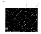
- FIG. 2 is a photograph of a magnetic material of the present disclosure.
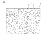
- FIG. 2 is a schematic diagram corresponding to FIG. 1 .
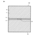
- 1 is a perspective view showing a schematic diagram of an electronic component according to an embodiment including a magnetic material according to the present disclosure; 4 is a schematic cross-sectional view taken along line a-a in FIG. 3.
- FIG. 13 is a perspective view illustrating an electronic component according to another embodiment.
- FIG. 1 is a photographic diagram showing the magnetic material of the present disclosure.
- FIG. 2 is a schematic diagram corresponding to FIG. 1.
- the inventors of the present application have been investigating and devising a new magnetic material with a different composition from conventional magnetic materials, in which soft magnetic powder is dispersed in resin, as this may lead to deterioration of high-frequency characteristics.
- the magnetic material 5 of the present disclosure is a sintered body 3 including a metal magnetic body 1 and a metal oxide or metal nitride 2 in which a non-magnetic metal is oxidized or nitrided.
- the above-mentioned metal oxide or metal nitride 2 is dispersed in the metal magnetic body 1.
- the filling rate of the metal magnetic body 1 in the magnetic material 5 is 81.4% or more and 99.2% or less.
- the above metal oxide or metal nitride 2 is an oxidized or nitrided non-magnetic metal, and therefore may have a higher electrical resistivity than the metal magnetic material.
- the electrical resistivity of the metal oxide or metal nitride may be 1 x 10 ⁇ 11 ⁇ cm or more and 1 x 10 ⁇ 16 ⁇ cm or less.
- the electrical resistivity of the metal magnetic material may be 0.089 ⁇ m or more and 1.76 ⁇ m or less.
- the above metal oxide or metal nitride 2 may itself be non-magnetic.
- the metal magnetic body 1 contains Fe element.
- the metal oxide or metal nitride 2 dispersed in the metal magnetic body 1 may be selected from at least one element selected from the group consisting of Si, Al, Cr, Ca, Mg, Ti, Mn, V, Zr, Nb, and Ta, which are elements more easily oxidized than Fe.
- the area ratio of the metal oxide or metal nitride 2 in the magnetic material 5 of the present disclosure may be 0.8% or more and 17.1% or less.
- the porosity of the magnetic material 5 of the present disclosure may be 0% or more and 1.5% or less.
- FIG. 3 is a perspective view showing a schematic diagram of an electronic component including the magnetic material of the present disclosure.
- FIG. 4 is a schematic cross-sectional view taken along line a-a in FIG. 3.
- the electronic component 100 comprises a base body 10 including the magnetic material 5 of the present disclosure, wiring 20, and external electrodes 30, 40.
- the base body 10 includes a sintered body 11.
- the sintered body 11 itself has at least one metallic magnetic sintered layer.
- the base body 10 may have a hexahedral structure.
- An insulating coating layer 60 may also be provided that covers the surface of the base body 10 except for the external electrodes 30, 40.
- the wiring 20 may be provided within the element body 10, for example.
- the wiring 20 is a conductive material, and may be at least one selected from the group consisting of silver, copper, aluminum, etc. As an example of the form of the wiring 20, it may be straight wiring as shown in FIG. 3. Without being limited to this, the wiring may be coil-shaped wiring.
- the external electrodes 30, 40 are provided on the surface of the element body 10. These external electrodes are respectively connected to both ends of the wiring 20, and are arranged opposite each other at a distance via the element body 10.
- the base body 10 contains the magnetic material 5 of the present disclosure, it contains a relatively high resistance metal oxide or metal nitride. This makes it possible to increase the electrical resistance of the path of the eddy current flowing through the sintered body 11 of the base body 10, thereby reducing eddy current loss. This eddy current loss increases as the current becomes higher in frequency, so reducing eddy current loss makes it possible to improve high frequency characteristics.
- the filling rate of the metal magnetic body 1 in the magnetic material 5 is 81.4% or more and 99.2% or less, and the filling rate of the metal magnetic body 1 in the sintered body 11 of the base body 10 can also be in the same range.
- the magnetic permeability i.e., the inductance value (L value)
- the portion of the magnetic material 5 other than the metal magnetic body (0.8% or more) excluding the voids contains relatively high-resistance metal oxides or metal nitrides. This makes it possible to reduce the above-mentioned eddy current loss.
- the area ratio of the metal oxide or metal nitride 2 in the magnetic material 5 is 0.8% or more and 17.1% or less, and the area ratio of the metal oxide or metal nitride 2 in the sintered body 11 of the base body 10 can be in the same range. Therefore, the electrical conductivity of the sintered body 11 as a whole can be reduced, and the Joule loss of the metal magnetic sintered body can be reduced.
- the void ratio of the magnetic material 5 is 0% or more and 1.5% or less, and the void ratio of the sintered body 11 of the base body 10 can be in the same range. Therefore, the space factor of the metal magnetic body can be suitably secured in the sintered body 11 as a whole. As a result, the decrease in storable magnetic energy can be suppressed, and the DC superposition characteristics are improved.
- the base body 10 further has a first insulating layer 13 in addition to the sintered body 11.
- This first insulating layer 13 can be continuous in a layered form from one side of the sintered body 11 to the other side in a direction intersecting the stacking direction L. With this form, two or more sintered bodies 11 separated by the first insulating layer 13 can be provided.
- the base body 10 has two or more sintered bodies 11 and a first insulating layer 13, and adjacent sintered bodies 11 and the other sintered body can be stacked with the first insulating layer 13 sandwiched between them.
- the first insulating layer 13 By providing the first insulating layer 13, a magnetic gap function can be provided compared to when the first insulating layer 13 is not provided.
- the first insulating layer 13 is nonmagnetic. This makes it possible to improve the DC superposition characteristics by reducing the magnetic permeability of the base body 10.
- the first insulating layer 13 can be a low-permeability insulating layer that is not nonmagnetic and has a magnetic permeability lower than that of the sintered body 11. In this case, inductance can also be improved compared to when it is nonmagnetic.
- the wiring 20 may be provided covered with an insulator without being limited to the form of the first insulating layer.
- the parts of the wiring 20 other than the two ends connected to the external electrodes 30, 40 are directly surrounded by the insulator. This allows the insulator to function as a magnetic gap. It is also preferable that the insulator is non-magnetic.
- the insulator can be a low-permeability insulator that is not nonmagnetic and has a lower magnetic permeability than the sintered body 11. In this case, it is possible to improve the inductance compared to the nonmagnetic case.
- the above-mentioned first insulating layer 13 may be provided in two or more pieces spaced apart from each other.
- the base body 10 has four sintered bodies 11.
- the wiring 20 is arranged between the first insulating layers 13, and the base body 10 may include three or more sintered bodies 11.
- a layered structure can be formed in which two or more sintered bodies 11 and the first insulating layers 13 are alternately stacked.
- the first external electrode 30 and the second external electrode 40 are arranged on the surfaces of different sintered bodies 11.
- the element body 10 can further have a second insulating layer 50.
- the first external electrode 30 and the second external electrode 40 are respectively arranged on the surfaces of adjacent sintered bodies 11, with the first external electrode 30 arranged on the surface of the sintered body 11 on one side and the second external electrode 30 arranged on the surface of the sintered body 11 on the other side.
- a second insulating layer 50 can be arranged between one sintered body 11 on which the first external electrode 30 is arranged and the sintered body 11 on which the second external electrode 40 is arranged.
- the second insulating layer 50 may be a slit-shaped tangible object that extends in a direction intersecting, for example, perpendicular to, the extension direction of the first insulating layer 13. Note that the second insulating layer 50 is not arranged so as to penetrate into and divide the wiring located inside the element body 10.
- the wiring does not necessarily have to be arranged inside the element body, and as shown in Figure 5, the wiring 20A may be arranged in a wound state on the outside of the element body 10A.
- the following describes a method for manufacturing electronic components that include the magnetic material disclosed herein.
- a metal magnetic particle containing an Fe component (e.g., FeNiCo-based particle) is prepared.
- a metal alkoxide containing a nonmagnetic metal element that is more easily oxidized than Fe is mixed with a solvent (water, alcohol, etc.) by a sol-gel method to hydrolyze the alkoxide in a slurry.
- the slurry is dried to obtain a metal magnetic particle whose surface is covered with a coating film containing an element that is more easily oxidized than Fe.
- a second coating film may be formed on the first coating film using a metal alkoxide containing a nonmagnetic metal element different from the nonmagnetic metal material used in the first coating film.
- the coating film may be one layer, two layers, or three or more layers.
- Metal alkoxides are represented by the chemical formula M(OR) x (M: non-magnetic metal element, OR: alkoxy group).
- the metal species M constituting the metal alkoxide may be at least one selected from the group consisting of Si, Al, Cr, Ca, Mg, Ti, Mn, V, Zr, Nb, and Ta.
- the metal alkoxide is preferably at least one alkoxide selected from the group consisting of Si, Ti, Al, and Zr.
- Si which is generally called a semimetal, is treated as a metallic element.
- the metal alkoxide is at least one alkoxide selected from the group consisting of Si, Ti, Al and Zr, a metal oxide having higher strength and higher resistivity can be formed.
- the alkoxy group OR constituting the metal alkoxide is not particularly limited, and may be, for example, an alkoxy group having 10 or less carbon atoms, particularly 5 or less, and more particularly 3 or less. The smaller the carbon number, the easier the hydrolysis reaction can be.
- the alkoxy group is preferably at least one selected from the group consisting of, for example, a methoxy group, an ethoxy group, and a propoxy group.
- the metal alkoxide is preferably at least one selected from the group consisting of tetraethyl orthosilicate, titanium tetraisopropoxide, zirconium n-butoxide, and aluminum isopropoxide.
- the slurry may contain a water-soluble polymer.
- the water-soluble polymer may be at least one selected from the group consisting of polyvinylpyrrolidone, polyvinyl alcohol, hydroxypropyl cellulose, poly(2-methyl-2-oxazoline), polyethyleneimine, polyacrylic acid, and carboxymethyl cellulose.
- a coating film containing an element that is more easily oxidized than Fe may be formed on the surface of the metal magnetic particles.
- the metal magnetic particles themselves may further contain an element that is more easily oxidized than Fe as a composition.
- a metal nitride component may be applied to the surface of the metal magnetic particles.
- metal oxides and metal nitrides of non-magnetic metals are non-magnetic.
- Non-magnetic insulating particles are prepared. Then, the insulating particles, varnish, a solvent (e.g., terpineol), and the like are mixed in a stirrer. Then, a dispersion process is performed in a roll mill to obtain an insulating paste.
- the non-magnetic insulator used in the insulating paste may be, for example, a mixture of alumina, silica, glass, or a dielectric material such as calcium zirconate, strontium zirconate, and/or barium zirconate with borosilicate glass, etc.
- the conductive particles can be copper particles, silver particles, etc.
- ⁇ Preparation step of unfired laminate> After preparing each paste, the above-mentioned metal magnetic paste is used to form a metal magnetic layer of a predetermined thickness by, for example, a screen printing method, and then dried. After drying, a slit groove of a predetermined width is formed by laser processing, and the above-mentioned insulating paste is filled into the slit groove by a screen printing method or the like, and then dried. Note that the slit groove is not limited to post-processing by laser processing, and may be previously patterned using a screen printing plate or the like.
- an insulating layer of a specified thickness is formed on the metal magnetic layer using the above insulating paste by screen printing and drying.
- the insulating paste used to form the insulating layer may be of a different type from the insulating paste filled into the slit grooves.
- wiring paste is used to form wiring in the desired shape (for example, straight shape, coil shape, meander shape, etc.) by screen printing.
- desired shape for example, straight shape, coil shape, meander shape, etc.
- via patterns that connect wiring patterns to each other are formed on multiple metal magnetic layers using wiring paste.
- the via pattern can be formed by first forming holes in the metal magnetic layer by laser processing or the like and filling them with wiring paste.
- an insulating layer may be further formed on top of it. The formation of the above metal magnetic layer and, optionally, the formation of an insulating layer are repeated to obtain an unsintered laminate.
- the L value of the resulting electronic component is higher than the desired characteristic, the number of insulating layers may be reduced or eliminated. This makes it possible to adjust the balance between the L value and the DC superposition characteristics.
- the above embodiment shows a method of laminating screen-printed layers formed using a screen printing method, but the present invention is not limited to this, and the electronic component may be produced by laminating sheets prepared separately.
- the unsintered laminate is cut into individual pieces using a dicer or the like, and then the individual pieces are degreased in a nitrogen atmosphere in a sintering furnace, and then sintered for a predetermined time (e.g., 1 hour) at a temperature of 900°C to 1000°C in a reducing atmosphere of H2 : 3%/ N2 : 97%.
- a predetermined time e.g. 1 hour
- the sintered body as the element may contain an oxide or nitride of an element that is more easily oxidized than Fe. Note that even if an element is more difficult to oxidize than Fe, it may be configured to be contained in the sintered laminate after being oxidized in a separate process.
- the above is based on the premise that a non-magnetic insulating layer is formed, but by extending the time that the maximum temperature is maintained during the above-mentioned firing, it is possible to diffuse the metal magnetic material components from the metal magnetic layer into the non-magnetic insulating layer, thereby obtaining an insulating layer with low magnetic permeability and some magnetic properties.
- the outer surface of the sintered body is then coated with an insulating resin or the like, and the coating at the portion where the wiring and the external electrodes are to be connected is peeled off with a laser or the like. Then, a plating process is performed to form the external electrodes, and finally, an electronic component is obtained.
- the material of the external electrodes can be, for example, silver.
- the powder was degreased in a nitrogen atmosphere and fired at 900°C for 60 minutes in a reducing atmosphere of H2 : 3% / N2 : 97%, to obtain a toroidal core and a cylindrical sample made of a magnetic metal sintered body.
- the toroidal core was wound and the magnetic permeability ⁇ (100 Hz) was measured using an impedance analyzer E4990A (Keysight).
- the cylindrical sample was measured using a vibration sample magnetometer VSM-5 (Toei Kogyo Co., Ltd.) to measure the saturation magnetic flux density Bs (16000 Oe).
- the measured ⁇ and Bs were entered into the following formula to calculate the B-H data.
- B Bs ⁇ tanh(4 ⁇ 10-7 ⁇ H/Bs)
- the Bs was calculated using the density of the metal material alone (Fe: 7.87 g/cm 3 , Ni: 8.9 g/cm 3 , Co: 8.9 g/cm 3 ) and the alloy density calculated from the composition ratio of each alloy.
- the calculated alloy densities are as follows: Fe10Ni20Co: 8.16g/ cm3
- the average value was taken from three arbitrary locations about halfway through the thickness of the sintered toroidal core.
- the average value was taken from six locations in total: three arbitrary locations located one time the wiring thickness above the top surface of the internal wiring, and three arbitrary locations located one time the wiring thickness below the bottom surface of the internal wiring. The method for visualizing high resistance areas will be described later.
- the values calculated above were used for the B-H curve of the magnetic material. Note that the B-H curve used portions with relative permeability ⁇ r of 1 or more so that it would not fall below the permeability of a vacuum, and was then extrapolated to the permeability of a vacuum using the functions of Femtet2022.
- the conductivity of the magnetic material was the value calculated above, and the iron loss was set to "Joule loss only (calculated from the current distribution)."
- the wiring material was silver.
- a straight silver wiring (length: width: thickness 1.0 mm: 0.0625 mm: 0.02 mm) was formed 0.315 mm from the bottom surface and in the center of the width dimension inside an element body with longitudinal dimension (L): width dimension (W): height (T) of 1.0 mm: 0.5 mm: 0.629 mm.
- non-magnetic insulating layers (longitudinal dimension (L): width dimension (W): height (T) of 1.0 mm: 0.5 mm: 0.002 mm) were formed in contact with the top and bottom surfaces of the straight wiring.
- a non-magnetic insulating layer (width 0.01 mm) was formed in the center of the longitudinal dimension (L) between the two external electrodes, separating them into two sintered bodies.
- Fe10Ni20Co particles with a D50 particle size of 0.40 ⁇ m were prepared.
- a slurry was prepared by mixing Si alkoxide and a solvent (water) by a sol-gel method, and the alkoxide was hydrolyzed in the slurry. After that, the slurry was dried to obtain metal magnetic particles whose surfaces were covered with a sol-gel coating film containing Si. The amount of this Si alkoxide was adjusted to appropriately set the target film thickness described later.
- the D50 particle size is not particularly limited, but may be 0.40 ⁇ m or more and 3.10 ⁇ m or less.
- Non-magnetic insulating particles of alumina with a D50 particle size of about 0.1 to 0.5 ⁇ m and non-magnetic insulating particles of borosilicate glass with a D50 particle size of about 0.1 to 0.5 ⁇ m were prepared. Then, these insulating particles were mixed with varnish and terpineol as a solvent in a stirrer. After that, a dispersion process was performed in a roll mill to obtain an insulating paste.
- ⁇ Preparation step of unfired laminate> After preparing each paste, the above-mentioned metal magnetic paste was used to form a metal magnetic layer of a predetermined thickness by screen printing, which was then dried. After drying, a slit groove of a predetermined width was formed by laser processing, and the above-mentioned insulating paste was filled into the slit groove by screen printing or the like, followed by drying.
- the slit grooves were filled with insulating paste and dried, after which an insulating layer of a specified thickness was formed on top of it using the above insulating paste by screen printing and then dried.
- the outer surface of the sintered body was then coated with an insulating resin, the coating at the portion where the wiring and the external electrodes were to be connected was removed with a laser, and then a plating process was performed to form the external electrodes.
- the material of the external electrodes may be, for example, silver. In this manner, an electronic component is obtained.
- Table 1 shows the results of measurements taken for each item, rather than a simulation, in which the metal magnetic paste was actually sintered to produce a sintered material, as explained in the sections ⁇ Metal magnetic paste preparation process> and ⁇ Singulation and sintering process of unsintered laminate>. No wiring or insulating layers were provided, and only the sintered material was produced.
- Table 2 shows the results of a simulation using the actual measurement data in Table 1.
- inductance (L) at 100 Hz must be 9 nH or more
- ⁇ L the rate of change of inductance (L) at 100 kHz relative to inductance (L) at 100 Hz
- the sintered body (magnetic material) which is a component of the element body contains a metal magnetic body and a silicon oxide dispersed in the metal magnetic body, and the filling rate of the metal magnetic body in the sintered body is 81.4% or more and 99.2% or less.
- the conductivity was the highest because SiO2 was not used. Therefore, the Joule loss, i.e., eddy current loss, of the obtained metal magnetic sintered body was large, which resulted in ⁇ L being -7.8%, and the overall evaluation was x.
- Examples 1 to 12 compared to Comparative Example 1, there was silicon oxide in the high resistance parts dispersed in the metal magnetic material, and specifically, the area ratio of the high resistance parts was 0.8% or more and 17.1% or less. As a result, the electrical conductivity was reduced, and the Joule loss of the obtained metal magnetic sintered body was reduced accordingly. As a result, in all of Examples 1 to 12, ⁇ L was -7% or more.
- the metal magnetic material was filled in the metal magnetic sintered body within a specified range, specifically, the filling rate was 81.4% or more and 99.2% or less, so that the magnetic permeability was also ensured to be equal to or higher than a specified value (25 or more). As a result, the inductance (L) at 100 Hz was ensured to be equal to or higher than 9 nH. From the above, the overall judgment was ⁇ in all of Examples 1 to 12.
- each sintered sample is resin-solidified and polished with a polishing machine Tegramin-25 (manufactured by Struers), then processed by FIB (focused ion beam) into a shape suitable for subsequent SPM (scanning probe microscope) measurement, and finally cleaned by Ar flat milling.
- Tegramin-25 manufactured by Struers
- FIB focused ion beam
- SSRM scanning spreading resistance microscope
- the high resistance area was defined as the area with a resistance value 10 ⁇ 3 times or more higher than the maximum measured resistance value of the metallic magnetic material, but the threshold value can be adjusted appropriately while referring to the element mapping image so that it matches the position of high resistance materials such as oxides and nitrides.
- FIG. 1 is an image of the sintered body produced in this example, taken at a magnification of 2000 times, visualizing the SiO2, which is a high resistance part.
- the colored parts are element mapping of the Si element.
- the other parts are metal magnetic bodies or voids. In this case, the grain boundary phase of the metal magnetic body particles in the metal magnetic body could not be confirmed even with a microscope.
- the present invention includes the following aspects, but is not limited to these aspects.
- ⁇ 1> A sintered body containing a metal magnetic body and a metal oxide or metal nitride in which a non-magnetic metal is oxidized or nitrided, the metal oxide or the metal nitride is dispersed in the metal magnetic material, A magnetic material in which the filling rate of the metal magnetic body is 81.4% or more and 99.2% or less.
- the metal magnetic body contains an Fe element
- ⁇ 3> The magnetic material according to ⁇ 1> or ⁇ 2>, wherein an area ratio of the metal oxide or the metal nitride in the magnetic material is 0.8% or more and 17.1% or less.
- ⁇ 4> The magnetic material according to any one of ⁇ 1> to ⁇ 3>, wherein the porosity is 0% or more and 1.5% or less.
- An electronic component comprising: an element body including the magnetic material according to any one of ⁇ 1> to ⁇ 4>; and wiring.
- ⁇ 6> The electronic component according to ⁇ 5>, which is an inductor.
- Electronic components containing the magnetic material disclosed herein can be used as inductors.
Landscapes
- Engineering & Computer Science (AREA)
- Power Engineering (AREA)
- Chemical & Material Sciences (AREA)
- Dispersion Chemistry (AREA)
- Physics & Mathematics (AREA)
- Electromagnetism (AREA)
- Microelectronics & Electronic Packaging (AREA)
- Coils Or Transformers For Communication (AREA)
Priority Applications (3)
| Application Number | Priority Date | Filing Date | Title |
|---|---|---|---|
| CN202480009135.6A CN120660156A (zh) | 2023-02-10 | 2024-02-05 | 磁性材料 |
| JP2024576323A JPWO2024166858A1 (https=) | 2023-02-10 | 2024-02-05 | |
| US19/265,387 US20250342991A1 (en) | 2023-02-10 | 2025-07-10 | Magnetic material |
Applications Claiming Priority (2)
| Application Number | Priority Date | Filing Date | Title |
|---|---|---|---|
| JP2023-019452 | 2023-02-10 | ||
| JP2023019452 | 2023-02-10 |
Related Child Applications (1)
| Application Number | Title | Priority Date | Filing Date |
|---|---|---|---|
| US19/265,387 Continuation US20250342991A1 (en) | 2023-02-10 | 2025-07-10 | Magnetic material |
Publications (1)
| Publication Number | Publication Date |
|---|---|
| WO2024166858A1 true WO2024166858A1 (ja) | 2024-08-15 |
Family
ID=92262559
Family Applications (1)
| Application Number | Title | Priority Date | Filing Date |
|---|---|---|---|
| PCT/JP2024/003688 Ceased WO2024166858A1 (ja) | 2023-02-10 | 2024-02-05 | 磁性材 |
Country Status (4)
| Country | Link |
|---|---|
| US (1) | US20250342991A1 (https=) |
| JP (1) | JPWO2024166858A1 (https=) |
| CN (1) | CN120660156A (https=) |
| WO (1) | WO2024166858A1 (https=) |
Citations (5)
| Publication number | Priority date | Publication date | Assignee | Title |
|---|---|---|---|---|
| JP2010087462A (ja) * | 2008-09-08 | 2010-04-15 | Toshiba Corp | コアシェル型磁性材料、コアシェル型磁性材料の製造方法、デバイス装置、およびアンテナ装置。 |
| JP2019169688A (ja) * | 2018-03-26 | 2019-10-03 | Tdk株式会社 | 軟磁性材料および圧粉磁心 |
| JP2020017690A (ja) * | 2018-07-27 | 2020-01-30 | 日本特殊陶業株式会社 | 圧粉磁心 |
| JP2020145405A (ja) * | 2019-02-28 | 2020-09-10 | 太陽誘電株式会社 | 軟磁性合金粉及びその製造方法、並びに軟磁性合金粉から作られるコイル部品及びそれを載せた回路基板 |
| JP2020155670A (ja) * | 2019-03-22 | 2020-09-24 | 日本特殊陶業株式会社 | 圧粉磁心 |
-
2024
- 2024-02-05 WO PCT/JP2024/003688 patent/WO2024166858A1/ja not_active Ceased
- 2024-02-05 JP JP2024576323A patent/JPWO2024166858A1/ja active Pending
- 2024-02-05 CN CN202480009135.6A patent/CN120660156A/zh active Pending
-
2025
- 2025-07-10 US US19/265,387 patent/US20250342991A1/en active Pending
Patent Citations (5)
| Publication number | Priority date | Publication date | Assignee | Title |
|---|---|---|---|---|
| JP2010087462A (ja) * | 2008-09-08 | 2010-04-15 | Toshiba Corp | コアシェル型磁性材料、コアシェル型磁性材料の製造方法、デバイス装置、およびアンテナ装置。 |
| JP2019169688A (ja) * | 2018-03-26 | 2019-10-03 | Tdk株式会社 | 軟磁性材料および圧粉磁心 |
| JP2020017690A (ja) * | 2018-07-27 | 2020-01-30 | 日本特殊陶業株式会社 | 圧粉磁心 |
| JP2020145405A (ja) * | 2019-02-28 | 2020-09-10 | 太陽誘電株式会社 | 軟磁性合金粉及びその製造方法、並びに軟磁性合金粉から作られるコイル部品及びそれを載せた回路基板 |
| JP2020155670A (ja) * | 2019-03-22 | 2020-09-24 | 日本特殊陶業株式会社 | 圧粉磁心 |
Also Published As
| Publication number | Publication date |
|---|---|
| US20250342991A1 (en) | 2025-11-06 |
| JPWO2024166858A1 (https=) | 2024-08-15 |
| CN120660156A (zh) | 2025-09-16 |
Similar Documents
| Publication | Publication Date | Title |
|---|---|---|
| JP5626834B2 (ja) | 開磁路型積層コイル部品の製造方法 | |
| TWI667669B (zh) | Magnetic materials and electronic parts | |
| TWI733759B (zh) | 積層電感器 | |
| TWI447756B (zh) | Coil parts | |
| JP2987176B2 (ja) | 積層型インダクタおよび積層型インダクタの製造方法 | |
| CN111009395B (zh) | 层叠型电子部件 | |
| JP7099345B2 (ja) | コイル部品 | |
| JP2024050965A (ja) | コイル部品 | |
| JP2021125598A (ja) | 積層コイル部品 | |
| JP2020061522A (ja) | 積層コイル部品 | |
| JP7444128B2 (ja) | フェライト磁器組成物及びコイル部品 | |
| JP2023027410A (ja) | コイル部品 | |
| JP2021108326A (ja) | 積層コイル部品 | |
| JP3975051B2 (ja) | 磁性フェライトの製造方法、積層型チップフェライト部品の製造方法及びlc複合積層部品の製造方法 | |
| JP2022064955A (ja) | 積層型コイル部品及びバイアスティー回路 | |
| WO2024166858A1 (ja) | 磁性材 | |
| JPH06333722A (ja) | 磁性フェライトの製造方法、磁性フェライト、積層型インダクタ部品、および複合積層部品 | |
| JP2001010820A (ja) | フェライト組成物、フェライト焼結体、積層型電子部品およびこれらの製造方法 | |
| US12469624B2 (en) | Magnetic base body and method of manufacturing magnetic base body | |
| US20250342992A1 (en) | Magnetic material and method for producing magnetic material | |
| WO2011148787A1 (ja) | 積層型インダクタおよびその製造方法 | |
| JP7608922B2 (ja) | 金属磁性体コア、インダクタ及び金属磁性体コアの製造方法 | |
| JP7251395B2 (ja) | 積層コイル部品 | |
| WO2024166857A1 (ja) | 電子部品 | |
| JP4449091B2 (ja) | 磁性フェライト材料、積層型チップフェライト部品、複合積層型部品および磁心 |
Legal Events
| Date | Code | Title | Description |
|---|---|---|---|
| 121 | Ep: the epo has been informed by wipo that ep was designated in this application |
Ref document number: 24753301 Country of ref document: EP Kind code of ref document: A1 |
|
| WWE | Wipo information: entry into national phase |
Ref document number: 2024576323 Country of ref document: JP |
|
| WWE | Wipo information: entry into national phase |
Ref document number: 202480009135.6 Country of ref document: CN |
|
| NENP | Non-entry into the national phase |
Ref country code: DE |
|
| WWP | Wipo information: published in national office |
Ref document number: 202480009135.6 Country of ref document: CN |
|
| 122 | Ep: pct application non-entry in european phase |
Ref document number: 24753301 Country of ref document: EP Kind code of ref document: A1 |