WO2024166459A1 - 電線 - Google Patents
電線 Download PDFInfo
- Publication number
- WO2024166459A1 WO2024166459A1 PCT/JP2023/039220 JP2023039220W WO2024166459A1 WO 2024166459 A1 WO2024166459 A1 WO 2024166459A1 JP 2023039220 W JP2023039220 W JP 2023039220W WO 2024166459 A1 WO2024166459 A1 WO 2024166459A1
- Authority
- WO
- WIPO (PCT)
- Prior art keywords
- layer
- electric wire
- mass
- ppm
- less
- Prior art date
- Legal status (The legal status is an assumption and is not a legal conclusion. Google has not performed a legal analysis and makes no representation as to the accuracy of the status listed.)
- Ceased
Links
Images



Classifications
-
- C—CHEMISTRY; METALLURGY
- C25—ELECTROLYTIC OR ELECTROPHORETIC PROCESSES; APPARATUS THEREFOR
- C25D—PROCESSES FOR THE ELECTROLYTIC OR ELECTROPHORETIC PRODUCTION OF COATINGS; ELECTROFORMING; APPARATUS THEREFOR
- C25D7/00—Electroplating characterised by the article coated
- C25D7/06—Wires; Strips; Foils
- C25D7/0607—Wires
-
- C—CHEMISTRY; METALLURGY
- C25—ELECTROLYTIC OR ELECTROPHORETIC PROCESSES; APPARATUS THEREFOR
- C25D—PROCESSES FOR THE ELECTROLYTIC OR ELECTROPHORETIC PRODUCTION OF COATINGS; ELECTROFORMING; APPARATUS THEREFOR
- C25D3/00—Electroplating: Baths therefor
- C25D3/02—Electroplating: Baths therefor from solutions
- C25D3/38—Electroplating: Baths therefor from solutions of copper
-
- C—CHEMISTRY; METALLURGY
- C25—ELECTROLYTIC OR ELECTROPHORETIC PROCESSES; APPARATUS THEREFOR
- C25D—PROCESSES FOR THE ELECTROLYTIC OR ELECTROPHORETIC PRODUCTION OF COATINGS; ELECTROFORMING; APPARATUS THEREFOR
- C25D5/00—Electroplating characterised by the process; Pretreatment or after-treatment of workpieces
- C25D5/34—Pretreatment of metallic surfaces to be electroplated
- C25D5/36—Pretreatment of metallic surfaces to be electroplated of iron or steel
-
- C—CHEMISTRY; METALLURGY
- C25—ELECTROLYTIC OR ELECTROPHORETIC PROCESSES; APPARATUS THEREFOR
- C25D—PROCESSES FOR THE ELECTROLYTIC OR ELECTROPHORETIC PRODUCTION OF COATINGS; ELECTROFORMING; APPARATUS THEREFOR
- C25D5/00—Electroplating characterised by the process; Pretreatment or after-treatment of workpieces
- C25D5/60—Electroplating characterised by the structure or texture of the layers
- C25D5/615—Microstructure of the layers, e.g. mixed structure
- C25D5/617—Crystalline layers
-
- H—ELECTRICITY
- H01—ELECTRIC ELEMENTS
- H01B—CABLES; CONDUCTORS; INSULATORS; SELECTION OF MATERIALS FOR THEIR CONDUCTIVE, INSULATING OR DIELECTRIC PROPERTIES
- H01B1/00—Conductors or conductive bodies characterised by the conductive materials; Selection of materials as conductors
- H01B1/02—Conductors or conductive bodies characterised by the conductive materials; Selection of materials as conductors mainly consisting of metals or alloys
- H01B1/026—Alloys based on copper
-
- C—CHEMISTRY; METALLURGY
- C25—ELECTROLYTIC OR ELECTROPHORETIC PROCESSES; APPARATUS THEREFOR
- C25D—PROCESSES FOR THE ELECTROLYTIC OR ELECTROPHORETIC PRODUCTION OF COATINGS; ELECTROFORMING; APPARATUS THEREFOR
- C25D3/00—Electroplating: Baths therefor
- C25D3/02—Electroplating: Baths therefor from solutions
- C25D3/12—Electroplating: Baths therefor from solutions of nickel or cobalt
Definitions
- Patent Document 1 electric wires having a core wire and a coating that covers the core wire have been used in automobiles and other vehicles.
- An electric wire comprises: An electric wire including a core wire and a coating covering the core wire,
- the core wire contains iron as a main component
- the coating comprises a first layer,
- the first layer contains copper as a main component,
- the first layer contains 10.5 ppm or more and 20.5 ppm or less of carbon on a mass basis.
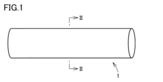
- FIG. 1 is a schematic perspective view of an electric wire according to an embodiment of the present disclosure.
- FIG. 2 is a schematic cross-sectional view taken along line II-II of FIG.
- FIG. 3 is a flow chart of a method for manufacturing an electric wire according to an embodiment of the present disclosure.
- FIG. 4 is an enlarged photograph of the cross section of the electric wire according to sample 101.
- FIG. 5 is an enlarged photograph of the cross section of the electric wire according to sample 1.
- FIG. 6 is an enlarged photograph of the cross section of the electric wire according to sample 101 after being exposed to a 250° C. environment for 1 hour and cooled in a 25° C. environment for 1 hour.
- FIG. 7 is an enlarged photograph of region VII in FIG. FIG.
- FIG. 8 is an enlarged photograph of the cross section of the electric wire according to Sample 1 after being exposed to a 250° C. environment for 1 hour and cooled in a 25° C. environment for 1 hour.
- FIG. 9 is a schematic perspective view of the sample electric wire cut in Evaluation Test 2.
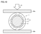
- FIG. 10 is a schematic cross-sectional view illustrating the evaluation method of Evaluation Test 2.
- FIG. 11 is a schematic cross-sectional view of an example of a sample electric wire of evaluation standard A′ in evaluation test 2.
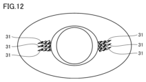
- FIG. 12 is a schematic cross-sectional view of an example of a sample electric wire of evaluation standard B′ in evaluation test 2.
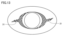
- FIG. 13 is a schematic cross-sectional view of another example of the electric wire sample of evaluation criterion B′ in evaluation test 2.
- FIG. 14 is a schematic perspective view illustrating the evaluation method of Evaluation Test 3.
- An electric wire may be heated when it is processed, when a current flows through the electric wire, and when it is used in a high-temperature environment. Therefore, when the electric wire has a core wire mainly containing iron and a copper layer covering the core wire, the thermal expansion coefficient of the core wire is different from that of the copper layer, and the core wire is generally harder than the copper layer. Due to this, when the temperature of the electric wire rises with heating, stress is applied to the copper layer. In addition, when the temperature of the electric wire rises with heating, crystal grains grow in the copper layer, and when a strong stress is applied to the electric wire from the outside, the crystal grains can become the starting point for cracking the copper layer.
- an object of the present disclosure is to provide an electric wire capable of suppressing peeling of a coating when an external stress is applied to an electric wire exposed to high temperatures.
- an electric wire that can suppress peeling of the coating when an external stress is applied to an electric wire exposed to high temperatures.
- An electric wire including a core wire and a coating covering the core wire,
- the core wire contains iron as a main component
- the coating comprises a first layer,
- the first layer contains copper as a main component,
- the first layer contains 10.5 ppm or more and 20.5 ppm or less of carbon on a mass basis.
- an electric wire that can suppress peeling of the coating when an external stress is applied to an electric wire exposed to high temperatures.
- the first layer may contain 11.5 ppm or more of carbon by mass. This makes it possible to provide an electric wire that can further suppress peeling of the coating when an external stress is applied to the electric wire exposed to high temperatures.
- the first layer may contain 16.5 ppm or less of carbon by mass. This makes it possible to provide an electric wire that can further suppress peeling of the coating when an external stress is applied to the electric wire exposed to high temperatures.
- the first layer may contain hydrogen in an amount of 0.35 ppm or more and 1.30 ppm or less by mass. This makes it possible to provide an electric wire that can further suppress peeling of the coating when an external stress is applied to the electric wire exposed to high temperatures.
- the first layer may contain 0.51 ppm or more of hydrogen by mass. This makes it possible to provide an electric wire that can further suppress peeling of the coating when an external stress is applied to the electric wire exposed to high temperatures.
- the first layer may contain 1.12 ppm or less of hydrogen by mass. This makes it possible to provide an electric wire that can further suppress peeling of the coating when an external stress is applied to the electric wire exposed to high temperatures.
- the first layer may contain 2.41 ppm or more and 5.62 ppm or less of oxygen by mass. This makes it possible to provide an electric wire that can further suppress peeling of the coating when an external stress is applied to the electric wire exposed to high temperatures.
- the first layer may contain 3.01 ppm or more of oxygen by mass. This makes it possible to provide an electric wire that can further suppress peeling of the coating when an external stress is applied to the electric wire exposed to high temperatures.
- the first layer may contain 5.01 ppm or less of oxygen by mass. This makes it possible to provide an electric wire that can further suppress peeling of the coating when an external stress is applied to the electric wire exposed to high temperatures.
- the first layer may contain 0.22 ppm to 0.65 ppm of sulfur by mass. This makes it possible to provide an electric wire that can further suppress peeling of the coating when an external stress is applied to the electric wire exposed to high temperatures.
- the first layer has crystal particles,
- the average grain size of the crystal grains may be 0.5 ⁇ m or more and 2 ⁇ m or less, thereby making it possible to provide an electric wire that can further suppress peeling of the coating when an external stress is applied to the electric wire exposed to high temperatures.
- the coating further includes a second layer, the second layer is located between the core wire and the first layer,
- the second layer contains nickel as a main component,
- the second layer may have a thickness of 0.3 nm to 40.3 nm, which makes it possible to provide an electric wire that can further suppress peeling of the coating when an external stress is applied to the electric wire exposed to high temperatures.
- the diameter of the core wire may be 0.10 mm or more and 0.20 mm or less. This makes it possible to provide an electric wire that can further suppress peeling of the coating when an external stress is applied to the electric wire exposed to high temperatures.
- the thickness of the first layer may be 0.04 mm or more and 0.06 mm or less. This makes it possible to provide an electric wire that can further suppress peeling of the coating when an external stress is applied to the electric wire exposed to high temperatures.
- the core wire may contain stainless steel or carbon steel. This makes it possible to provide an electric wire that can further suppress peeling of the coating when an external stress is applied to the electric wire exposed to high temperatures.
- this embodiment is not limited thereto.
- an expression in the form of "A to B” means the upper and lower limits of a range (i.e., A or more and B or less).
- a or more and B or less the upper and lower limits of a range
- An electric wire 1 according to an embodiment of the present disclosure will be described with reference to FIGS. 1 and 2 .
- One embodiment of the present disclosure (hereinafter also referred to as “the present embodiment") is An electric wire 1 including a core wire 2 and a coating 5 covering the core wire 2,
- the core wire 2 contains iron as a main component
- the coating 5 comprises a first layer 4,
- the first layer 4 contains copper as a main component,
- the first layer 4 contains 10.5 ppm or more and 20.5 ppm or less of carbon on a mass basis.
- the coating that constitutes the electric wire When processing an electric wire, the coating that constitutes the electric wire may be heated. Furthermore, when a current flows through the electric wire, the electric wire generates heat, which may heat up the coating that constitutes the electric wire. Furthermore, electric wires are used in high-temperature environments, which may heat up the coating that constitutes the electric wire. When the coating is heated, the crystal grains that constitute the coating grow. As a result, when columnar crystals are formed in the coating in the thickness direction of the coating, the crystal grain boundaries extend in the thickness direction, making it easy for cracks to occur in the thickness direction. The core wire and the coating that covers the core wire are easily peeled off from the cracks.
- the coating 5 includes a first layer 4, which contains copper as a main component and 10.5 ppm to 20.5 ppm of carbon by mass. This makes it easier to suppress grain growth of crystal grains containing copper. As a result, the grain boundaries of the crystal grains in the first layer 4 are suppressed from extending in the film thickness direction, making it difficult for cracks to occur in the film thickness direction. Therefore, peeling between the core wire 2 and the coating 5 covering the core wire 2, which starts from the crack, can be suppressed.
- an electric wire 1 that can suppress peeling of the coating 5 when external stress is applied to the electric wire 1 exposed to high temperatures.
- the electric wire 1 includes a core wire 2.
- the core wire 2 contains iron as a main component.
- iron means “iron element”.
- the core wire 2 contains iron as a main component” means “the core wire 2 contains 50% by mass or more of iron”.
- the lower limit of the iron content in the core wire 2 can be 51% by mass or more, 52% by mass or more, 53% by mass or more, or 73% by mass or more.
- the upper limit of the iron content can be 100% by mass or less, 99% by mass or less, or 98% by mass or less.
- the content can be 51% by mass or more and 100% by mass or less, 52% by mass or more and 99% by mass or less, or 53% by mass or more and 98% by mass or less.
- ICP Inductively Coupled Plasma
- the core wire 2 may contain stainless steel or carbon steel. This facilitates alloying with the first layer 4, further improving the peel resistance of the coating 5 when an external stress is applied to the electric wire 1 exposed to high temperatures.
- stainless steel refers to steel with an iron content of 74% by mass or less, a nickel content of 8% by mass or more, and a chromium content of 18% by mass or more.
- the stainless steel may contain inevitable impurities. Examples of the inevitable impurities include carbon (0.01% by mass to 0.08% by mass), silicon (0.1% by mass to 1.0% by mass), manganese (0.1% by mass to 2.0% by mass), phosphorus (0.01% by mass to 0.045% by mass), and sulfur (0.01% by mass to 0.03% by mass).
- An example of the material of the stainless steel is SUS304.
- iron means “iron element”.
- Nickel means “nickel element”.
- Chromium means “chromium element”.
- Carbon means “carbon element”.
- Sicon means “silicon element”.
- Manganese means “manganese element”.
- Phosphorus means “elemental phosphorus”.
- Sulfur means “elemental sulfur”.
- Carbon steel refers to steel with an iron content of 97.9% by mass to 99.8% by mass and a carbon content of 0.02% by mass to 2.14% by mass.
- the carbon steel may contain inevitable impurities.
- the inevitable impurities include sulfur (0.01% by mass to 0.03% by mass), phosphorus (0.001% by mass to 0.01% by mass), and silicon (0.01% by mass to 0.05% by mass).
- An example of a material for the carbon steel is piano wire. Note that "iron” means “elemental iron”. "Carbon” means “elemental carbon”.
- sulfur means “elemental sulfur”.
- Phosphorus means “elemental phosphorus”.
- Silicon means “elemental silicon”.
- the carbon content in the core wire 2, the chromium content in the core wire 2, the nickel content in the core wire 2, the silicon content in the core wire 2, the manganese content in the core wire 2, the phosphorus content in the core wire 2, and the sulfur content in the core wire 2 can be determined by a method similar to the measurement method for the "iron content in the core wire 2" described above.
- the diameter R of the core wire 2 may be 0.10 mm or more and 0.20 mm or less. This makes it difficult for breakage or cracking to occur when stress is applied from the outside of the electric wire 1, and therefore the peel resistance of the coating 5 can be further improved when stress is applied from the outside to the electric wire 1 exposed to high temperatures.
- the lower limit of the diameter R may be 0.10 mm or more, 0.12 mm or more, 0.14 mm or more, or 0.15 mm or more.
- the upper limit of the diameter R may be 0.20 mm or less, 0.19 mm or less, or 0.17 mm or less.
- the diameter R may be 0.12 mm or more and 0.19 mm or less, or 0.14 mm or more and 0.17 mm or less.
- the diameter R of the core wire 2 can be obtained by the following method. That is, first, the electric wire 1 having a length of 20 mm obtained by cutting the electric wire 1 on a plane perpendicular to the longitudinal direction is embedded in resin. Next, one of the cut surfaces of the electric wire 1 embedded in resin is pre-finished by mechanical polishing, and a cross-section polisher (CP) is applied with an Ar ion beam under the following conditions to obtain a polished cut surface. Next, CP-SEM (Scanning Electron Microscopy) is performed on the polished cut surface using a high-resolution scanning electron microscope "SU8020" manufactured by Hitachi High-Tech Corporation, and a 500x image is obtained so that the entire cut surface after polishing is included in one field of view.
- CP-SEM Sccanning Electron Microscopy
- the length of the longest line segment among the line segments connecting the any one point and a point located on the outer periphery is obtained.
- the length of the longest line segment is similarly obtained for any four further points.
- the diameter R can be determined by calculating the average length of these longest line segments.
- the electric wire 1 includes a coating 5 that coats the core wire 2.
- the coating 5 may have a thickness of 41 ⁇ m or more and 65 ⁇ m or less. If the coating 5 has a thickness of less than 41 ⁇ m, the electrical conductivity of the coating 5 tends to decrease. If the coating 5 has a thickness of more than 65 ⁇ m, the wire drawability in a later process tends to decrease.
- the coating 5 may have a thickness of 45 ⁇ m or more and 63 ⁇ m or less, or may have a thickness of 50 ⁇ m or more and 60 ⁇ m or less.
- the thickness of the coating 5 means the average value of the thickness of the coating 5 in the cross section of the electric wire 1.
- the measurement method will be described in more detail below. Specifically, first, a scanning electron microscope (SEM) is used to obtain microscopic images of five arbitrary cross sections of the electric wire 1. Next, five arbitrary points are selected on the outer periphery (outermost surface) of the electric wire 1 in each of the above images, and the shortest distance from the outer periphery to the core wire 2 at each point is determined, and this is taken as the thickness of the coating 5. The thickness of the coating 5 is measured at a total of 25 points, and an average value is calculated from the values obtained, which can be taken as the thickness of the coating 5. If there are clearly abnormal values in the above measurement, these abnormal values are excluded and the average value is calculated. If there are three or more abnormal values, the same number of measurements are performed as an alternative, and the average value is calculated using the values obtained thereby.
- SEM scanning electron microscope
- the coating 5 includes a first layer 4.
- the first layer 4 may be in contact with the outer circumferential surface of the core wire 2, or may not be in contact with the outer circumferential surface of the core wire 2.
- a second layer 3 which will be described later, another layer, or both, may be present between the core wire 2 and the first layer 4.
- the coating 5 may be composed of only the first layer 4, or may be composed of only the first layer 4 and the second layer 3, which will be described later.
- the first layer 4 contains copper as a main component. This allows the first layer 4 to impart electrical conductivity to the electric wire 1.
- “copper” means “elemental copper”.
- the first layer 4 contains copper as a main component
- the first layer 4 contains 99% by mass or more of copper.
- the lower limit of the copper content in the first layer 4 may be 99.99 mass% or more, 99.991 mass% or more, or 99.992 mass% or more.
- the upper limit of the copper content may be 99.999 mass% or less, 99.998 mass% or less, or 99.997 mass% or less.
- the copper content may be 99.99 mass% or more and 99.999 mass% or less, 99.991 mass% or more and 99.998 mass% or less, or 99.992 mass% or more and 99.997 mass% or less.
- the copper content in the first layer 4 can be determined by the following method. That is, it can be determined by performing a D-SIMS (Dynamic Secondary Ion Mass Spectrometry) analysis under the following conditions.
- D-SIMS Dynamic Secondary Ion Mass Spectrometry
- the first layer 4 contains 10.5 ppm or more and 20.5 ppm or less of carbon by mass. This creates a pinning effect and slows down the movement of grain boundaries, making it easier to suppress the growth of crystal grains in the first layer. This improves the peeling resistance of the coating 5 when external stress is applied to the electric wire 1 exposed to high temperatures.
- the lower limit of the carbon content in the first layer 4 may be 11.5 ppm or more, 12.0 ppm or more, or 12.3 ppm or more by mass.
- the upper limit of the carbon content in the first layer 4 may be 16.5 ppm or less, 15.5 ppm or less, or 14.4 ppm or less by mass.
- the carbon content in the first layer 4 may be 11.5 ppm or more and 16.5 ppm or less, 12.0 ppm or more and 15.5 ppm or less, or 12.3 ppm or more and 14.4 ppm or less, based on mass.
- carbon means “elemental carbon.”
- the first layer 4 may contain hydrogen in an amount of 0.35 ppm or more and 1.30 ppm or less by mass. This provides a pinning effect, slowing down the movement of grain boundaries, making it easier to suppress the growth of crystal grains in the first layer. This further improves the peel resistance of the coating 5 when external stress is applied to the electric wire 1 exposed to high temperatures.
- the lower limit of the hydrogen content in the first layer 4 may be 0.35 ppm or more, 0.51 ppm or more, or 0.67 ppm or more by mass.
- the upper limit of the hydrogen content in the first layer 4 may be 1.30 ppm or less, 1.12 ppm or less, or 0.94 ppm or less by mass.
- the hydrogen content in the first layer 4 may be 0.51 ppm or more and 1.12 ppm or less, or 0.67 ppm or more and 0.94 ppm or less by mass.
- hydrogen means "elemental hydrogen.”
- the first layer 4 may contain oxygen in an amount of 2.41 ppm or more and 5.62 ppm or less by mass. This provides a pinning effect, slowing down the movement of grain boundaries, making it easier to suppress the growth of crystal grains in the first layer. This further improves the peel resistance of the coating 5 when external stress is applied to the electric wire 1 exposed to high temperatures.
- the lower limit of the oxygen content in the first layer 4 may be 2.41 ppm or more by mass, 3.01 ppm or more, or 3.12 ppm or more.
- the upper limit of the oxygen content in the first layer 4 may be 5.62 ppm or less by mass, 5.01 ppm or less, or 4.32 ppm or less.
- the oxygen content in the first layer 4 may be 3.01 ppm or more and 5.01 ppm or less, or 3.12 ppm or more and 4.32 ppm or less.
- oxygen means "elemental oxygen.”
- the first layer 4 may contain sulfur in an amount of 0.22 ppm or more and 0.65 ppm or less by mass. This provides a pinning effect and slows down the movement of grain boundaries, making it easier to suppress the growth of crystal grains in the first layer. This further improves the peel resistance of the coating 5 when external stress is applied to the electric wire 1 exposed to high temperatures.
- the lower limit of the sulfur content in the first layer 4 may be 0.22 ppm or more, 0.25 ppm or more, or 0.29 ppm or more by mass.
- the upper limit of the sulfur content in the first layer 4 may be 0.65 ppm or less, 0.55 ppm or less, or 0.45 ppm or less by mass.
- the sulfur content in the first layer 4 may be 0.25 ppm or more and 0.55 ppm or less, or 0.29 ppm or more and 0.45 ppm or less by mass.
- sulfur means "elemental sulfur.”
- the first layer 4 may contain unavoidable impurities as long as the wire 1 has both electrical conductivity and peel resistance.
- the unavoidable impurities include nitrogen, phosphorus, and silicon.
- the content of the unavoidable impurities can be determined by the same method as the method for measuring the copper content in the first layer 4.
- the thickness T1 of the first layer 4 may be 0.04 mm or more and 0.06 mm or less. This facilitates mutual diffusion of heat between the core wire 2 and the coating 5, thereby further improving the peel resistance of the coating 5 when an external stress is applied to the electric wire 1 exposed to high temperatures.
- the lower limit of the thickness T1 of the first layer 4 may be 0.04 mm or more, 0.045 mm or more, or 0.050 mm or more.
- the upper limit of the thickness T1 of the first layer 4 may be 0.06 mm or less, 0.058 mm or less, or 0.056 mm or less.
- the thickness T1 of the first layer 4 may be 0.045 mm or more and 0.058 mm or less, or 0.050 mm or more and 0.056 mm or less.
- the thickness T1 of the first layer 4 can be determined in the same manner as the thickness of the coating 5, except for the following: "If the first layer 4 is present on the outermost surface of the coating 5, the shortest distance from the outer circumference to the interface of the first layer 4 on the core wire 2 side is determined, and this is taken as the thickness T1 of the first layer 4. If the first layer 4 is not present on the outermost surface of the coating 5, the shortest distance from the interface on the surface side of the first layer 4 to the interface of the first layer 4 on the core wire 2 side is determined, and this is taken as the thickness T1 of the first layer 4.”
- the first layer 4 has crystal grains, and the average grain size of the crystal grains may be 0.5 ⁇ m or more and 2 ⁇ m or less. This makes it difficult for grain boundaries to reach from the surface of the coating 5 to the core wire 2 even if grain growth occurs, and therefore the peeling resistance of the coating 5 can be further improved when external stress is applied to the electric wire 1 exposed to high temperatures.
- the lower limit of the average grain size of the crystal grains may be 0.5 ⁇ m or more, 0.7 ⁇ m or more, or 0.9 ⁇ m or more.
- the upper limit of the average grain size of the crystal grains may be 2 ⁇ m or less, 1.4 ⁇ m or less, or 1.1 ⁇ m or less.
- the average grain size of the crystal grains may be 0.7 ⁇ m or more and 1.4 ⁇ m or less, or 0.9 ⁇ m or more and 1.1 ⁇ m or less.
- the average grain size of the crystal grains can be determined by the following method. That is, first, a 20 mm electric wire 1 obtained by cutting along a plane perpendicular to the longitudinal direction is embedded in resin. Next, one of the cut surfaces of the electric wire 1 embedded in resin is pre-finished by mechanical polishing, and a cross-section polisher (CP) is applied with an Ar ion beam under the following conditions to obtain a polished cut surface. Next, CP-SEM (Scanning Electron Microscopy) is performed on the polished cut surface using a high-resolution scanning electron microscope "SU8020" manufactured by Hitachi High-Tech Corporation, and a 5000x image is obtained so that the entire cut surface after polishing is included in one field of view.
- CP-SEM Sccanning Electron Microscopy
- crystal grain size of each crystal grain is calculated by the following formula (1), and the average value is taken as the average grain size of the crystal grains.
- crystal grain diameter ⁇ (Crystal grain width)+(Crystal grain height) ⁇ /2 (1)
- crystal grain width means the maximum distance between two points located on the outer edge of the crystal grain to be measured, where a virtual line passing through the two points is perpendicular to the thickness direction of the coating.
- crystal grain height means the maximum distance between two points located on the outer edge of the crystal grain to be measured, where a virtual line passing through the two points is parallel to the thickness direction of the coating.
- the number of crystal grains to be measured is 10 in one visual field of the same first layer, and the number of visual fields is 20. Note that one visual field is a rectangle with a length of 12 ⁇ m and a width of 9.6 ⁇ m.
- the coating 5 further includes a second layer 3, which is located between the core wire 2 and the first layer 4, and may include nickel as a main component. This allows the iron element of the core wire 2, the copper element of the coating 5, and the nickel element of the coating 5 to form a metallic bond when thermal diffusion occurs, thereby further improving the peeling resistance of the coating 5 when stress is applied from the outside to the electric wire 1 exposed to high temperatures.
- the second layer 3 may be in contact with the outer circumferential surface of the core wire 2 or may not be in contact with the outer circumferential surface of the core wire 2.
- nickel here means “elemental nickel”.
- the second layer 3 contains nickel as a main component” means “the second layer 3 contains 90% by mass or more of nickel”.
- the lower limit of the nickel content in the second layer 3 can be 91% by mass or more, 92% by mass or more, 93% by mass or more, or 99% by mass or more.
- the upper limit of the content can be 100% by mass or less, 99% by mass or less, or 98% by mass or less.
- the content can be 91% by mass or more and 100% by mass or less, 92% by mass or more and 99% by mass or less, or 93% by mass or more and 98% by mass or less.
- the nickel content in the second layer 3 can be determined by the following method. That is, the nickel content can be determined by the following procedure.
- a cross section of the electric wire 1 is obtained by cutting the electric wire 1 in a plane perpendicular to the longitudinal direction.
- microsampling processing is performed on the cross section using a focused ion beam (FIB) of "Quanta3D" manufactured by FEI company in the United States.
- the microsampling processing includes rough processing and finishing processing.
- the rough processing is performed under conditions of 30 kV, and the finishing processing is performed under conditions of 8 kV.
- the nickel content in the observation field is measured by performing EDX analysis on the image at 200 kV using a JEM-2100F manufactured by JEOL Ltd.
- the nickel content in the second layer 3 can be determined by calculating the average nickel content in a total of five observation fields.
- the second layer 3 may contain unavoidable impurities as long as the electric wire 1 has peel resistance.
- the unavoidable impurities include carbon, silicon, and sulfur.
- the content of the unavoidable impurities can be determined by the same method as the method for measuring the nickel content in the second layer 3.
- the thickness T2 of the second layer 3 may be 0.3 nm or more and 40.3 nm or less. This allows the iron element of the core wire and the copper element or nickel element of the coating to be metallically bonded when thermal diffusion occurs, and therefore the peel resistance of the coating 5 can be further improved when external stress is applied to the electric wire 1 exposed to high temperatures.
- the lower limit of the thickness T2 of the second layer 3 may be 0.3 nm or more, 5 nm or more, or 10 nm or more.
- the upper limit of the thickness T2 of the second layer 3 may be 40.3 nm or less, 30 nm or less, or 20 nm or less.
- the thickness T2 of the second layer 3 may be 5 nm or more and 30 nm or less, or 10 nm or more and 20 nm or less.
- the thickness T2 of the second layer 3 can be determined in the same manner as the thickness of the coating 5, except that "the shortest distance from the interface on the surface side of the second layer 3 to the interface on the core wire 2 side of the second layer 3 is determined, and this is taken as the thickness T2 of the second layer 3."
- the coating 5 may further include other layers, such as a Ni--Cu layer and an Fe--Ni trilayer .
- the thickness of the other layer can be determined in the same manner as the thickness of the coating 5 described above, except that "if the other layer is located on the outermost surface of the coating 5, the shortest distance from the outer circumference to the interface of the other layer on the core wire 2 side is determined, and this is the thickness of the other layer. If the other layer is not located on the outermost surface of the coating 5, the shortest distance from the interface on the surface side of the other layer to the interface of the other layer on the core wire 2 side is determined, and this is the thickness of the other layer.”
- Fig. 3 is a flow chart of the method for producing an electric wire according to an embodiment of the present disclosure.
- the method for producing an electric wire according to the present embodiment is the method for producing the electric wire according to the first embodiment, A first step of preparing a core wire containing iron as a main component; A second step of forming a coating on an outer circumferential surface of the core wire, The second step includes a first layer forming step of forming a first layer on the outer peripheral surface of the core wire.
- the second step may further include a second layer forming step of forming a second layer on the outer peripheral surface of the core wire before the first layer forming step.
- a core wire containing iron as a main component is prepared.
- the first step of preparing the core wire can be performed, for example, by preparing a core wire made of stainless steel containing iron as a main component, or carbon steel containing iron as a main component, etc. Note that in the first step, a step of degreasing the outer peripheral surface of the core wire and washing with water after the degreasing may be performed.
- a coating is formed on the outer circumferential surface of the core wire.
- the second step includes a "first layer forming step” of forming a first layer on the outer circumferential surface of the core wire.
- the second step may further include a "second layer forming step” of forming a second layer on the outer circumferential surface of the core wire before the "first layer forming step”.
- the second step may include a step of forming the other layer in addition to the "first layer covering step” or the "first layer covering step” and the "second layer covering step”.
- the other layer may be formed by a conventional method.
- a second layer is formed on the outer peripheral surface of the core wire prior to the "first layer forming step".
- the second layer forming step can be performed, for example, by forming the second layer on the outer peripheral surface of the core wire by electrolytic plating using a Wood's bath.
- a first layer is formed on the outer peripheral surface of the core wire.
- the first layer forming step can be performed, for example, by forming the first layer on the outer peripheral surface of the core wire by electrolytic plating using copper sulfate plating.
- a step of washing the outer peripheral surface of the first layer with water may be performed.
- an electrolytic plating bath containing additives is used.
- additives refer to polymers, levelers, and brighteners.
- the polymer content, leveler content, and brightener content are each 1 mg/L or more and 15 mg/L or less. This allows the carbon content, hydrogen content, and sulfur content in the first layer to be adjusted to the desired range, thereby improving the peel resistance of the coating when an external stress is applied to an electric wire exposed to high temperatures. This was newly discovered by the present inventors as a result of extensive research.
- the electrolytic plating bath may be a copper sulfate plating bath.
- polymer polyethylene glycol (PEG).
- leveler is bis(3-sulfopropyl) disulfide (SPS).
- SPS bis(3-sulfopropyl) disulfide
- JGB Janus Green B
- the lower limit of the content of the additive in the electrolytic plating may be 1.5 mg/L or more, 2 mg/L or more, or 3 mg/L or more.
- the upper limit of the content of the additive in the electrolytic plating may be 13 mg/L or less, 10 mg/L or less, or 8 mg/L or less.
- the content of the additive in the electrolytic plating may be 1.5 mg/L or more and 13 mg/L or less, 2 mg/L or more and 10 mg/L or less, or 3 mg/L or more and 8 mg/L or less.
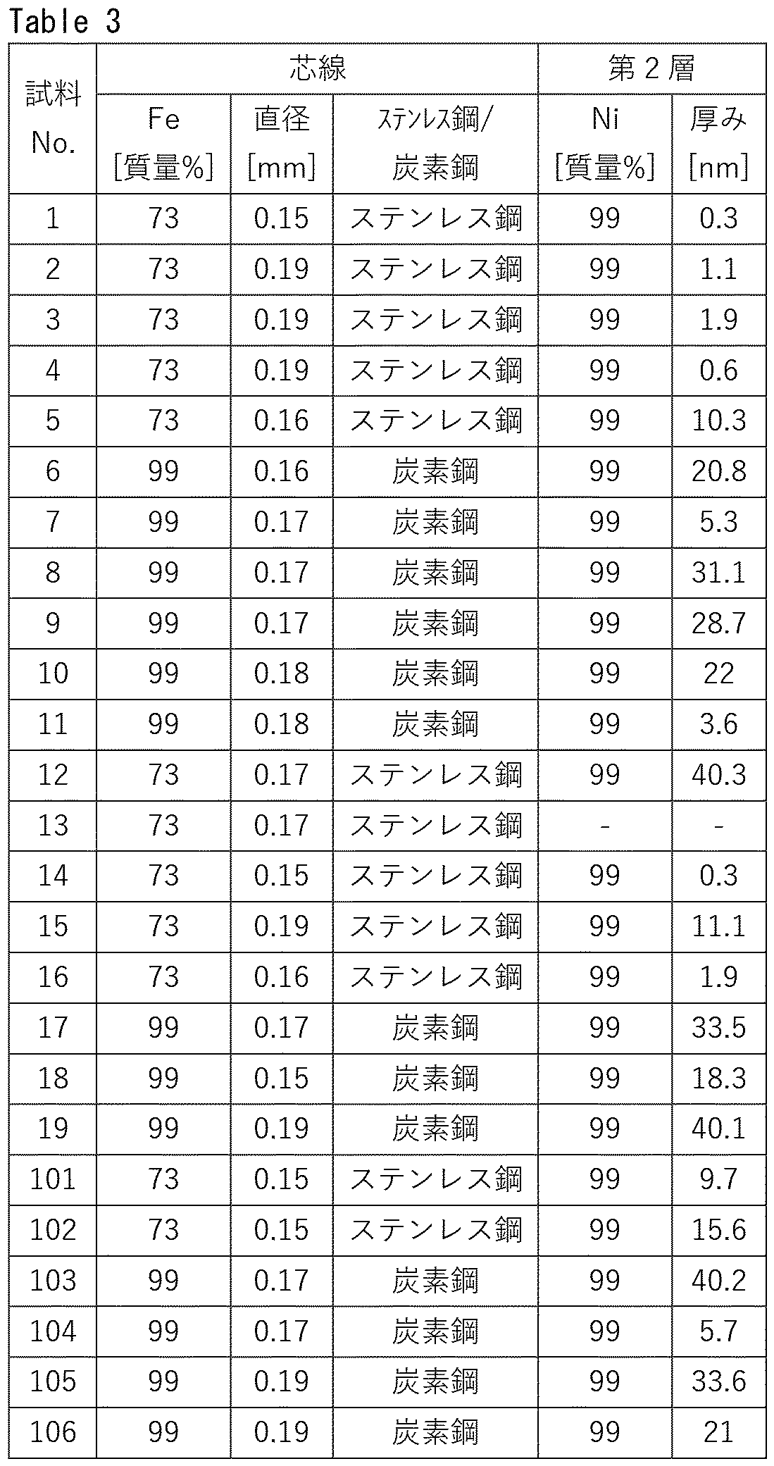
- a "degreasing step” was performed on the outer peripheral surface of a core wire having the configuration shown in Table 3 under the following conditions using a degreasing liquid ("Ace Clean 220" (trademark) manufactured by Okuno Chemical Industries Co., Ltd.), and then a “water-rinsing step” was performed under the following conditions. Note that when “stainless steel” or “carbon steel” is listed in the "Stainless steel/carbon steel” column in Table 3, it means that the core wire contains “stainless steel” or “carbon steel.” (Degreasing process conditions) Temperature: 50°C Time: 10 seconds (conditions for water washing process) Immersion time: 10 seconds
- electrolytic plating is performed on the outer peripheral surface of the core wire after the water washing step using a Wood's bath having the composition and pH shown in Table 1 under the temperature and current density conditions shown in Table 1.
- the second layer forming step was carried out by electrolytic plating.
- the electrolytic plating time was the time required for the second layer to have a thickness as shown in Table 3.
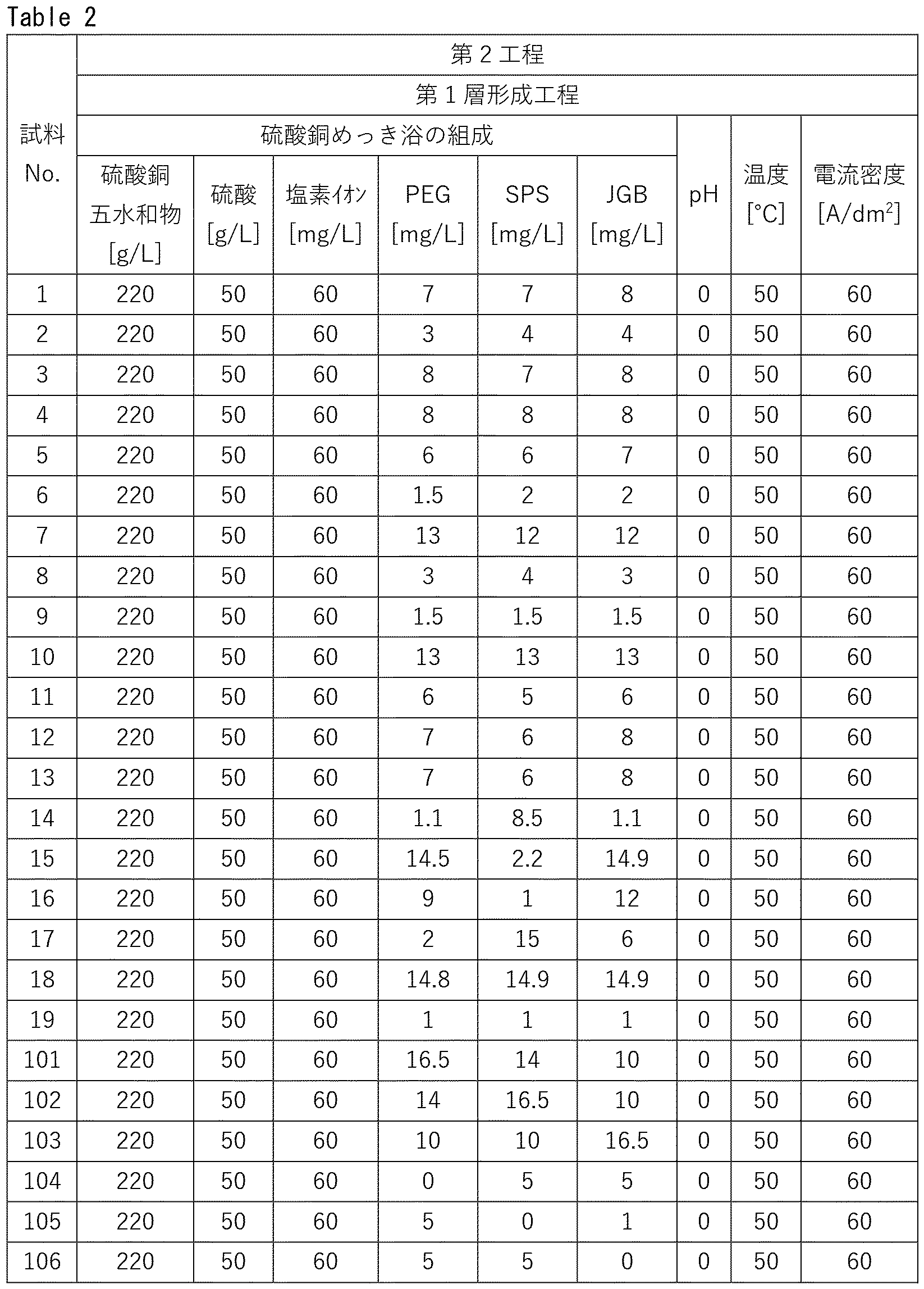
- Second process Next, the outer peripheral surface of the second layer formed in the second layer forming step was plated with a copper sulfate plating (electrolytic plating) bath having the composition and pH shown in Table 2 at a temperature shown in Table 2.
- the first layer was formed by carrying out the first layer formation step under the conditions of and current density.
- the electrolytic plating time was the time until the thickness of the first layer reached the values shown in Table 4. did.
- the oxygen content in the first layer was determined by the method described in the first embodiment. The results obtained are shown in the "O [ppm]” column of Table 4.
- the sulfur content in the first layer was determined by the method described in Embodiment 1. The results obtained are shown in the column “S [ppm]” in Table 4.
- FIG. 4 is an enlarged photograph of the cross section of the electric wire according to Sample 101.
- FIG. 5 is an enlarged photograph of the cross section of the electric wire according to Sample 1.
- FIG. 6 is an enlarged photograph of the cross section of the electric wire of sample 101 after being exposed to an environment of 250°C for 1 hour and cooled in an environment of 25°C for 1 hour as described above.
- FIG. 7 is an enlarged photograph of region VII in FIG. 6. In FIG. 7, the point indicated by the arrow indicates the point where the grain boundary of the crystal grain extends in the film thickness direction.
- FIG. 8 is an enlarged photograph of the cross section of the electric wire of sample 1 after being exposed to an environment of 250°C for 1 hour and cooled in an environment of 25°C for 1 hour as described above.
- the larger the average grain size of the crystal grains the more likely it is that cracks will occur, and the more likely the coating will peel off from the cracks. Therefore, a large average grain size of the crystal grains in evaluation test 1 means that the coating has a reduced peel resistance when an external stress is applied to the electric wire exposed to high temperatures.
- Fig. 9 is a schematic perspective view of the sample electric wire 1 cut in the evaluation test 2.
- Fig. 10 is a schematic cross-sectional view illustrating the evaluation method of the evaluation test 2.
- Fig. 11 is a schematic cross-sectional view of an example of the sample electric wire of the evaluation criterion A' of the evaluation test 2.
- Fig. 12 is a schematic cross-sectional view of an example of the sample electric wire of the evaluation criterion B' of the evaluation test 2.
- Fig. 13 is a schematic cross-sectional view of another example of the sample electric wire of the evaluation criterion B' of the evaluation test 2.
- the electric wires 1 according to the samples 1 to 19 and the samples 101 to 106 were exposed to an environment of 250°C for 1 hour.
- the electric wires 1 according to the samples 1 to 19 and the samples 101 to 106 were cooled in an environment of 25°C for 1 hour.
- the electric wires 1 according to the samples 1 to 19 and the samples 101 to 106 were cut to a length of 50 mm as shown in Fig. 9.
- the electric wire 1 after being cut to a length of 50 mm was sandwiched between stainless steel plates 20a and 20b.
- the evaluation criterion A' described later specifically means the state shown in FIG. 11, and the evaluation criterion B' described later specifically means the state shown in FIG. 12 and FIG. 13. Furthermore, if a crack occurs at the interface of the first layer on the core wire side, the coating is likely to peel off from the crack, and therefore the occurrence of a crack means that the peel resistance of the coating has decreased when external stress is applied to the electric wire exposed to high temperatures, even if peeling has not yet occurred.
- Fig. 14 is a schematic perspective view illustrating the evaluation method of Evaluation Test 3.
- the electric wires 1 according to Samples 1 to 19 and Samples 101 to 106 were exposed to an environment of 250°C for one hour.
- the electric wires 1 according to Samples 1 to 19 and Samples 101 to 106 were cooled in an environment of 25°C for one hour.
- the electric wires 1 according to Samples 1 to 19 and Samples 101 to 106 were wound five times in the direction of the arrow around a wire 22 having a cross-sectional diameter of 0.25 mm as an axis (self-diameter bending).
- the electric wires according to samples 1 to 19 correspond to the examples, and the electric wires according to samples 101 to 106 correspond to the comparative examples.
- the electric wires according to samples 1 to 15 and 17 have significantly more suppressed crystal grain growth caused by exposure to high temperatures than the electric wires according to samples 101 to 106, and have less reduction in peel resistance of the coating when stress is applied from the outside to the electric wires exposed to high temperatures.
- the electric wires according to samples 1 to 16, 18 and 19 have significantly improved peel resistance of the coating when stress is applied from the outside to the electric wires exposed to high temperatures than the electric wires according to samples 101 to 106.
- the electric wires according to the above samples 1 to 19 can prevent the coating from peeling off when an external stress is applied to an electric wire exposed to high temperatures.
Landscapes
- Chemical & Material Sciences (AREA)
- Engineering & Computer Science (AREA)
- Chemical Kinetics & Catalysis (AREA)
- Electrochemistry (AREA)
- Materials Engineering (AREA)
- Metallurgy (AREA)
- Organic Chemistry (AREA)
- Crystallography & Structural Chemistry (AREA)
- Non-Insulated Conductors (AREA)
Abstract
Description
芯線と、該芯線を被覆する被膜と、を備える電線であって、
該芯線は、鉄を主成分として含み、
該被膜は、第1層を含み、
該第1層は、銅を主成分として含み、
該第1層は、質量基準で10.5ppm以上20.5ppm以下の炭素を含む。
電線は、該電線の加工の際、該電線に電流が流れる際、及び該電線が高温の環境で使用される際において、加熱される場合がある。その為、該電線が、鉄を主成分として含む芯線と、該芯線を被覆する銅層とを備える場合において、該芯線の熱膨張率と該銅層の熱膨張率とが異なることと、該芯線が該銅層よりも一般的に硬いこととに起因して、該電線の温度が加熱に伴い上昇する際、該銅層に応力が加わることとなる。また、該電線の温度が加熱に伴い上昇した場合において、該銅層中で結晶粒子の成長が生じ、該電線に外部から強い応力が加わる際、該結晶粒子は該銅層が割れる起点となり得る。よって、従来の電線は、該応力と該結晶粒子の成長とに起因して、加熱に伴い銅層の芯線側の界面に亀裂が生じ、該亀裂を生じた箇所を起点として、該銅層が剥離し易い場合があった。その為、高温に曝された電線に外部から応力が印加されたときに被膜が剥離するのを抑制することが求められている。
[本開示の効果]
最初に本開示の実施態様を列記して説明する。
[1]本開示の一態様に係る電線は、
芯線と、前記芯線を被覆する被膜と、を備える電線であって、
前記芯線は、鉄を主成分として含み、
前記被膜は、第1層を含み、
前記第1層は、銅を主成分として含み、
前記第1層は、質量基準で10.5ppm以上20.5ppm以下の炭素を含む。
前記結晶粒子の平均粒径は、0.5μm以上2μm以下であってもよい。これによって、高温に曝された電線に外部から応力が印加されたときに被膜が剥離するのを更に抑制することが可能な電線を提供することができる。
前記第2層は、前記芯線と前記第1層との間に位置し、
前記第2層は、ニッケルを主成分として含み、
前記第2層の厚みは、0.3nm以上40.3nm以下であってもよい。これによって、高温に曝された電線に外部から応力が印加されたときに被膜が剥離するのを更に抑制することが可能な電線を提供することができる。
以下、本開示の一実施形態(以下「本実施形態」と記す。)について説明する。ただし、本実施形態はこれに限定されるものではない。本明細書において「A~B」という形式の表記は、範囲の上限下限(すなわちA以上B以下)を意味し、Aにおいて単位の記載がなく、Bにおいてのみ単位が記載されている場合、Aの単位とBの単位とは同じである。
本開示の一実施形態に係る電線1について、図1及び図2を用いて説明する。
本開示の一実施形態(以下、「本実施形態」とも記す。)は、
芯線2と、該芯線2を被覆する被膜5と、を備える電線1であって、
該芯線2は、鉄を主成分として含み、
該被膜5は、第1層4を含み、
該第1層4は、銅を主成分として含み、
該第1層4は、質量基準で10.5ppm以上20.5ppm以下の炭素を含む。
<芯線の組成>
上記電線1は、芯線2を備える。該芯線2は、鉄を主成分として含む。ここで、「鉄」とは、「鉄元素」を意味する。また、「芯線2は、鉄を主成分として含む」とは、「芯線2は、50質量%以上の鉄を含む」ことを意味する。芯線2における鉄の含有率の下限は、51質量%以上、52質量%以上、53質量%以上、73質量%以上とすることができる。該含有率の上限は、100質量%以下、99質量%以下、98質量%以下とすることができる。該含有率は、51質量%以上100質量%以下、52質量%以上99質量%以下、53質量%以上98質量%以下とすることができる。
上記芯線2の直径Rは、0.10mm以上0.20mm以下であってもよい。これによって、電線1の外部から応力が印加されたときに断線や割れが発生し難くなる為、高温に曝された電線1に外部から応力が印加されたときにおける被膜5の耐剥離性を更に向上することができる。該直径Rの下限は、0.10mm以上であってもよく、0.12mm以上であってもよく、0.14mm以上であってもよく、0.15mm以上であってもよい。該直径Rの上限は、0.20mm以下であってもよく、0.19mm以下であってもよく、0.17mm以下であってもよい。該直径Rは、0.12mm以上0.19mm以下であってもよく、0.14mm以上0.17mm以下であってもよい。
(CPの条件)
・加速電圧:1.0kV
・傾斜:0゜
上記電線1は、上記芯線2を被覆する被膜5を備える。該被膜5の厚みは、41μm以上65μm以下であってもよい。該被膜5の厚みが41μm未満であると、被膜5の導電性が低下する傾向がある。該被膜5の厚みが65μm超であると、後工程の伸線性が低下する傾向がある。該被膜5の厚みは、45μm以上63μm以下であってもよく、50μm以上60μm以下であってもよい。
(第1層の組成)
上記被膜5は、第1層4を含む。ここで、該第1層4は、上記芯線2の外周面上に接していても良く、上記芯線2の外周面上に接していなくても良い。該第1層4が該芯線2の外周面上に接していない場合においては、該芯線2と該第1層4との間に、後述する第2層3、他の層、またはその両方が存在し得る。被膜5は、第1層4のみからなっていてもよく、第1層4および後述する第2層3のみからなっていてもよい。また、該第1層4は、銅を主成分として含む。これによって、該第1層4は、上記電線1に電気伝導性を付与することができる。ここで、「銅」とは、「銅元素」を意味する。また、「第1層4は、銅を主成分として含む」とは、「第1層4は、99質量%以上の銅を含む」ことを意味する。該第1層4における銅の含有率の下限は、99.99質量%以上、99.991質量%以上、99.992質量%以上とすることができる。該含有率の上限は、99.999質量%以下、99.998質量%以下、99.997質量%以下とすることができる。該含有率は、99.99質量%以上99.999質量%以下、99.991質量%以上99.998質量%以下、99.992質量%以上99.997質量%以下とすることができる。
(D-SIMSの条件)
・装置:CAMECA社製の「IMS6f」
・1次イオン種:Cs+
・加速電圧:15kV
・分析領域:30μmΦ
上記第1層4の厚みT1は、0.04mm以上0.06mm以下であってもよい。これによって、芯線2と被膜5との間で熱の相互拡散が生じ易くなる為、高温に曝された電線1に外部から応力が印加されたときにおける被膜5の耐剥離性を更に向上することができる。該第1層4の厚みT1の下限は、0.04mm以上であってもよく、0.045mm以上であってもよく、0.050mm以上であってもよい。該第1層4の厚みT1の上限は、0.06mm以下であってもよく、0.058mm以下であってもよく、0.056mm以下であってもよい。該第1層4の厚みT1は、0.045mm以上0.058mm以下であってもよく、0.050mm以上0.056mm以下であってもよい。
(結晶粒子の粒径)={(結晶粒子の幅)+(結晶粒子の高さ)}/2 (1)
ここで、「結晶粒子の幅」とは、測定対象の結晶粒における外縁に位置する2点間の最大距離であって、当該2点を通る仮想線が上記被膜の厚み方向に対して垂直である、2点間の最大距離を意味する。「結晶粒子の高さ」とは、測定対象の結晶粒における外縁に位置する2点間の最大距離であって、当該2点を通る仮想線が上記被膜の厚み方向に対して平行である、2点間の最大距離を意味する。測定する当該結晶粒子の数は、同一の第1層の1視野において任意の10個であり、該視野の数は20視野である。なお、1つの視野は、縦12μm×幅9.6μmの長方形である。
(CPの条件)
・加速電圧:1.0kV
・傾斜:0゜
(第2層の組成)
上記被膜5は、第2層3を更に含み、該第2層3は、該芯線2と該第1層4との間に位置し、該第2層3は、ニッケルを主成分として含んでもよい。これによって、熱拡散が生じた際に、芯線2の鉄元素、被膜5の銅元素、及び被膜5のニッケル元素が金属結合する為、高温に曝された電線1に外部から応力が印加されたときにおける被膜5の耐剥離性を更に向上することができる。ここで、該第2層3が該芯線2と該第1層4との間に位置する限りにおいて、該第2層3は、該芯線2の外周面上に接していても良く、該芯線2の外周面上に接していなくても良い。該第2層3が該芯線2の外周面上に接していない場合においては、該芯線2と該第2層3との間に、後述する他の層が存在し得る。また、該第2層3が該芯線2と該第1層4との間に位置する限りにおいて、該第1層4は、該第2層3の外周面上に接していても良く、該第2層3の外周面上に接していなくても良い。該第1層4が該第2層3の外周面上に接していない場合においては、該第2層3と該第1層4との間に、後述する他の層が存在し得る。また、ここで「ニッケル」とは、「ニッケル元素」を意味する。また、「第2層3は、ニッケルを主成分として含む」とは、「第2層3は、90質量%以上のニッケルを含む」ことを意味する。該第2層3におけるニッケルの含有率の下限は、91質量%以上、92質量%以上、93質量%以上、99質量%以上とすることができる。該含有率の上限は、100質量%以下、99質量%以下、98質量%以下とすることができる。該含有率は、91質量%以上100質量%以下、92質量%以上99質量%以下、93質量%以上98質量%以下とすることができる。
上記第2層3の厚みT2は、0.3nm以上40.3nm以下であってもよい。これによって、熱拡散が生じた際に、芯線の鉄元素と、被膜の銅元素またはニッケル元素とが金属結合する為、高温に曝された電線1に外部から応力が印加されたときにおける被膜5の耐剥離性を更に向上することができる。該第2層3の厚みT2の下限は、0.3nm以上であってもよく、5nm以上であってもよく、10nm以上であってもよい。該第2層3の厚みT2の上限は、40.3nm以下であってもよく、30nm以下であってもよく、20nm以下であってもよい。該第2層3の厚みT2は、5nm以上30nm以下であってもよく、10nm以上20nm以下であってもよい。
上記被膜5は、他の層を更に含み得る。該他の層としては、Ni-Cu層、Fe-Ni3層などが挙げられる。
本実施形態の電線の製造方法について図3を用いて説明する。図3は、本開示の一実施形態に係る電線の製造方法のフローチャートである。本実施形態の電線の製造方法は、図3に示される様に、実施形態1に記載の電線の製造方法であって、
主成分として鉄を含む芯線を準備する第1工程と、
該芯線の外周面上に被膜を形成する第2工程と、を含み、
該第2工程は、該芯線の外周面上に第1層を形成する第1層形成工程を含む。該第1層形成工程において、1mg/L以上15mg/L以下の添加剤を含む電解めっき浴を用いる。また、本実施形態の電線の製造方法において、該第2工程は、該第1層形成工程の前に、該芯線の外周面上に第2層を形成する第2層形成工程を更に含むことができる。
第1工程において、主成分として鉄を含む芯線を準備する。該芯線を準備する第1工程は、たとえば、主成分として鉄を含むステンレス鋼、または主成分として鉄を含む炭素鋼などの芯線を準備することにより行なうことができる。なお、該第1工程において、該芯線の外周面を脱脂し、該脱脂後に水洗する工程を行なってもよい。
第2工程において、該芯線の外周面上に被膜を形成する。該第2工程は、該芯線の外周面上に第1層を形成する「第1層形成工程」を含む。該第2工程は、該「第1層形成工程」の前に、該芯線の外周面上に第2層を形成する「第2層形成工程」を更に含むことができる。該第2工程は、該「第1層被覆工程」、または該「第1層被覆工程」と該「第2層被覆工程」とに加えて、上記他の層を形成する工程を含むことができる。該他の層は、従来の方法によって形成することができる。
第2層形成工程において、該「第1層形成工程」の前に、該芯線の外周面上に第2層を形成する。該第2層形成工程は、たとえば、ウッド浴を用いた電解めっきにより、該芯線の外周面上に第2層を形成することにより行なうことができる。
第1層形成工程において、該芯線の外周面上に第1層を形成する。該第1層形成工程は、たとえば、硫酸銅めっきを用いた電解めっきにより、該芯線の外周面上に該第1層を形成することにより行なうことができる。なお、該第1層形成工程の後に、該第1層の外周面を水洗する工程を行なってもよい。
以下の様にして、試料1~19及び試料101~106に係る電線を作製した。
まず、表3に記載の構成を有する芯線の外周面に対し、脱脂液(奥野製薬工業株式会社製の「エースクリーン220」(商標))を用いて以下の条件で「脱脂工程」を行なった後に、以下の条件で「水洗工程」を行なった。なお、表3の「ステンレス鋼/炭素鋼」欄に「ステンレス鋼」または「炭素鋼」が記載されている場合は、芯線が「ステンレス鋼」または「炭素鋼」を含んでいることを意味する。
(脱脂工程の条件)
温度:50℃
時間:10秒
(水洗工程の条件)
浸漬時間:10秒
次に、上記水洗工程を行なった後の芯線の外周面上に、表1に記載の組成及びpHを有するウッド浴を用いて、表1に記載の温度及び電流密度の条件で電解めっきを実行することによって、第2層形成工程を行なった。なお、該電解めっきの時間は、第2層の厚みが表3に記載の通りとなるまでの時間とした。また、表1の「第2層形成工程」欄の全ての欄に「-」と記載されている場合は、第2層形成工程が実行されなかったことを意味する。
次に、上記第2層形成工程で形成された第2層の外周面上に、表2に記載の組成及びpHを有する硫酸銅めっき(電解めっき)浴を用いて、表2に記載の温度及び電流密度の条件で第1層形成工程を行なうことにより、第1層を形成した。なお、該電解めっきの時間は、第1層の厚みが表4に記載の通りとなるまでの時間とした。
(水洗工程の条件)
浸漬時間:10秒

<第1層の組成>
試料1~19及び試料101~106に係る電線に関し、上記第1層における銅の含有率を実施形態1に記載の方法により求めた。得られた結果をそれぞれ表4の「Cu[ppm]」の欄に記す。また、試料1~19及び試料101~106に係る電線に関し、上記第1層における炭素の含有率を実施形態1に記載の方法により求めた。得られた結果をそれぞれ表4の「C[ppm]」の欄に記す。また、試料1~19及び試料101~106に係る電線に関し、上記第1層における水素の含有率を実施形態1に記載の方法により求めた。得られた結果をそれぞれ表4の「H[ppm]」の欄に記す。また、試料1~19及び試料101~106に係る電線に関し、上記第1層における酸素の含有率を実施形態1に記載の方法により求めた。得られた結果をそれぞれ表4の「O[ppm]」の欄に記す。また、試料1~19及び試料101~106に係る電線に関し、上記第1層における硫黄の含有率を実施形態1に記載の方法により求めた。得られた結果をそれぞれ表4の「S[ppm]」の欄に記す。
試料1~19及び試料101~106に係る電線に関し、上記第1層における結晶粒子の平均粒径を実施形態1に記載の方法により求めた。得られた結果をそれぞれ表4の「結晶粒子の平均粒径[μm]」の欄に記す。なお、図4は、試料101に係る電線の横断面の拡大写真である。また、図5は、試料1に係る電線の横断面の拡大写真である。
試料1~19及び試料101~106に係る電線に関し、上記第2層におけるニッケルの含有率を実施形態1に記載の方法により求めた。得られた結果をそれぞれ表3の「Ni[質量%]」の欄に記す。なお、表3の「第2層」欄の全ての欄に「-」と記載されている場合は、第2層が存在しないことを意味する。
試料1~19及び試料101~106に係る電線に関し、上記被膜の厚みを実施形態1に記載の方法により求めた。得られた結果をそれぞれ表4の「被膜の厚み[mm]」の欄に記す。
先ず、上記試料1~19及び試料101~106に係る電線を250℃の環境に1時間曝露した。次に該試料1~19及び試料101~106に係る電線を25℃の環境下で1時間冷却した。次に、該試料1~19及び試料101~106に係る電線について、第1層における結晶粒子の平均粒径を実施形態1に記載の方法により求めた。得られた結果を表4の「評価試験1」の欄に記す。なお、評価基準は以下の通りとした。
(評価試験1の評価基準)
A:結晶粒子の平均粒径が3μm以上10μm以下。
B:結晶粒子の平均粒径が10μm超。
評価試験2の方法について、図9から図13を用いて以下の通り説明する。図9は、評価試験2において切断された試料の電線1の模式的な斜視図である。図10は、評価試験2の評価方法を図解する模式的な断面図である。図11は、評価試験2の評価基準A’の試料の電線の一例の模式的な断面図である。図12は、評価試験2の評価基準B’の試料の電線の一例の模式的な断面図である。図13は、評価試験2の評価基準B’の試料の電線の他の一例の模式的な断面図である。先ず、上記試料1~19及び試料101~106に係る電線1を250℃の環境に1時間曝露した。次に該試料1~19及び試料101~106に係る電線1を25℃の環境下で1時間冷却した。次に、該試料1~19及び試料101~106に係る電線1を図9に示すように50mmの長さに切断した。次に、図10に示すように、50mmの長さに切断した後の電線1をステンレス鋼板20a、20bの間に挟み込んだ。次に、電線1の横断面の直径が40%減少するように、ステンレス鋼板20bを固定した状態で、ステンレス鋼板20aから矢印21の方向に6000Nの圧力を電線1に印加した。次に、該圧力の印加後の試料1~19及び試料101~106の電線1の第1層4の外周面のSEMの150倍像を取得し、試料1~19及び試料101~106の電線1の第1層4の外周面の評価を後述する評価基準により行なった。得られた結果を表4の「評価試験2」の欄に記す。なお、評価試験2において、後述する評価基準A’とは、具体的には図11に示される状態を意味し、後述する評価基準B’とは、具体的には図12及び図13に示される状態を意味する。また、第1層の芯線側の界面にクラックが生じると、該クラックを起点として被膜の剥離が生じ易くなることから、該クラックが生じていれば、未だ該剥離が生じていなかったとしても、高温に曝された電線に外部から応力が印加されたときの被膜の耐剥離性が低下していることを意味する。
評価試験3の方法について、図14を用いて以下の通り説明する。図14は、評価試験3の評価方法を図解する模式的な斜視図である。先ず、上記試料1~19及び試料101~106に係る電線1を250℃の環境に1時間曝露した。次に該試料1~19及び試料101~106に係る電線1を25℃の環境下で1時間冷却した。次に、図14に示される様に、該試料1~19及び試料101~106に係る電線1を、横断面の直径が0.25mmである線22を軸にして、矢印の方向に5回巻き付けた(自己径曲げ)。次に、該自己径曲げ後の試料1~19及び試料101~106の電線1の第1層の外周面について、SEM(Scanning Electron Microscope)の150倍像を取得し、試料1~19及び試料101~106の電線1の第1層の外周面の評価を以下の評価基準により行なった。得られた結果を表4の「評価試験3」の欄に記す。なお、結晶粒子が大きいほど結晶粒界を起点に芯線まで到達するクラックが発生し易くなる。第1層の外周面にクラックが生じていれば、高温に曝された電線に外部から応力が印加されたときの被膜の耐剥離性が低下していることを意味する。
(評価試験2及び評価試験3の評価基準)
A’:クラック31が発生しなかった。
B’:クラック31が発生した。

Claims (15)
- 芯線と、前記芯線を被覆する被膜と、を備える電線であって、
前記芯線は、鉄を主成分として含み、
前記被膜は、第1層を含み、
前記第1層は、銅を主成分として含み、
前記第1層は、質量基準で10.5ppm以上20.5ppm以下の炭素を含む、電線。 - 前記第1層は、質量基準で11.5ppm以上の炭素を含む、請求項1に記載の電線。
- 前記第1層は、質量基準で16.5ppm以下の炭素を含む、請求項1または請求項2に記載の電線。
- 前記第1層は、質量基準で0.35ppm以上1.30ppm以下の水素を含む、請求項1から請求項3のいずれか1項に記載の電線。
- 前記第1層は、質量基準で0.51ppm以上の水素を含む、請求項4に記載の電線。
- 前記第1層は、質量基準で1.12ppm以下の水素を含む、請求項4または請求項5に記載の電線。
- 前記第1層は、質量基準で2.41ppm以上、5.62ppm以下の酸素を含む、請求項1から請求項6のいずれか1項に記載の電線。
- 前記第1層は、質量基準で3.01ppm以上の酸素を含む、請求項7に記載の電線。
- 前記第1層は、質量基準で5.01ppm以下の酸素を含む、請求項7または請求項8に記載の電線。
- 前記第1層は、質量基準で0.22ppm以上0.65ppm以下の硫黄を含む、請求項1から請求項9のいずれか1項に記載の電線。
- 前記第1層は、結晶粒子を有し、
前記結晶粒子の平均粒径は、0.5μm以上2μm以下である、請求項1から請求項10のいずれか1項に記載の電線。 - 前記被膜は、第2層を更に含み、
前記第2層は、前記芯線と前記第1層との間に位置し、
前記第2層は、ニッケルを主成分として含み、
前記第2層の厚みは、0.3nm以上40.3nm以下である、請求項1から請求項11のいずれか1項に記載の電線。 - 前記芯線の直径は、0.10mm以上0.20mm以下である、請求項1から請求項12のいずれか1項に記載の電線。
- 前記第1層の厚みは、0.04mm以上0.06mm以下である、請求項1から請求項13のいずれか1項に記載の電線。
- 前記芯線は、ステンレス鋼または炭素鋼を含む、請求項1から請求項14のいずれか1項に記載の電線。
Priority Applications (3)
| Application Number | Priority Date | Filing Date | Title |
|---|---|---|---|
| JP2024576104A JPWO2024166459A1 (ja) | 2023-02-10 | 2023-10-31 | |
| DE112023005768.0T DE112023005768T5 (de) | 2023-02-10 | 2023-10-31 | Elektrischer Draht |
| CN202380089202.5A CN120418891A (zh) | 2023-02-10 | 2023-10-31 | 电线 |
Applications Claiming Priority (2)
| Application Number | Priority Date | Filing Date | Title |
|---|---|---|---|
| JP2023-018992 | 2023-02-10 | ||
| JP2023018992 | 2023-02-10 |
Publications (1)
| Publication Number | Publication Date |
|---|---|
| WO2024166459A1 true WO2024166459A1 (ja) | 2024-08-15 |
Family
ID=92262818
Family Applications (1)
| Application Number | Title | Priority Date | Filing Date |
|---|---|---|---|
| PCT/JP2023/039220 Ceased WO2024166459A1 (ja) | 2023-02-10 | 2023-10-31 | 電線 |
Country Status (4)
| Country | Link |
|---|---|
| JP (1) | JPWO2024166459A1 (ja) |
| CN (1) | CN120418891A (ja) |
| DE (1) | DE112023005768T5 (ja) |
| WO (1) | WO2024166459A1 (ja) |
Citations (2)
| Publication number | Priority date | Publication date | Assignee | Title |
|---|---|---|---|---|
| WO2011162301A1 (ja) * | 2010-06-24 | 2011-12-29 | 株式会社フジクラ | 自動車用電線 |
| WO2020031268A1 (ja) * | 2018-08-07 | 2020-02-13 | 住友電気工業株式会社 | 銅被覆鋼線および撚線 |
-
2023
- 2023-10-31 JP JP2024576104A patent/JPWO2024166459A1/ja active Pending
- 2023-10-31 DE DE112023005768.0T patent/DE112023005768T5/de active Pending
- 2023-10-31 WO PCT/JP2023/039220 patent/WO2024166459A1/ja not_active Ceased
- 2023-10-31 CN CN202380089202.5A patent/CN120418891A/zh active Pending
Patent Citations (2)
| Publication number | Priority date | Publication date | Assignee | Title |
|---|---|---|---|---|
| WO2011162301A1 (ja) * | 2010-06-24 | 2011-12-29 | 株式会社フジクラ | 自動車用電線 |
| WO2020031268A1 (ja) * | 2018-08-07 | 2020-02-13 | 住友電気工業株式会社 | 銅被覆鋼線および撚線 |
Also Published As
| Publication number | Publication date |
|---|---|
| JPWO2024166459A1 (ja) | 2024-08-15 |
| DE112023005768T5 (de) | 2025-11-20 |
| CN120418891A (zh) | 2025-08-01 |
Similar Documents
| Publication | Publication Date | Title |
|---|---|---|
| CN101809177B (zh) | 电气电子部件用铜合金板材 | |
| TWI878425B (zh) | Cu-Ni-Si系銅合金板材及其製造方法和通電零件 | |
| TWI605559B (zh) | Bonding wire for semiconductor device | |
| JP6380174B2 (ja) | 銀めっき付き銅端子材及び端子 | |
| JP4809935B2 (ja) | 低ヤング率を有する銅合金板材およびその製造法 | |
| KR101682791B1 (ko) | 감합형 접속 단자용 Sn 피복층 부착 구리 합금판 및 감합형 접속 단자 | |
| JP5400877B2 (ja) | 銅合金板材およびその製造方法 | |
| US20030025182A1 (en) | Metal article coated with tin or tin alloy under tensile stress to inhibit whisker growth | |
| WO2009148101A1 (ja) | 銅合金板材およびその製造方法 | |
| WO2016031654A1 (ja) | 耐微摺動摩耗性に優れる接続部品用導電材料 | |
| JP5144814B2 (ja) | 電気電子部品用銅合金材料 | |
| JP2016164991A (ja) | 半導体装置用ボンディングワイヤ | |
| JP2014208904A (ja) | 耐摩耗性に優れる接続部品用導電材料 | |
| JP2012177153A (ja) | 銅合金 | |
| CN114466942A (zh) | 连接器用端子材 | |
| JP7773020B2 (ja) | コネクタ用端子材 | |
| JP4934785B2 (ja) | Snめっき銅合金材料およびその製造方法 | |
| KR20100095431A (ko) | 동합금 판재 | |
| JP5897084B1 (ja) | 耐微摺動摩耗性に優れる接続部品用導電材料 | |
| JP5897083B1 (ja) | 耐微摺動摩耗性に優れる接続部品用導電材料 | |
| JP5690169B2 (ja) | 銅合金 | |
| WO2024166459A1 (ja) | 電線 | |
| JP2013231224A (ja) | 曲げ加工性に優れた電気・電子部品用銅合金材 | |
| JP2009084593A (ja) | Cu−Cr−Si系合金箔 | |
| TWI918991B (zh) | Cu-Ti系銅合金板材、其製造方法、通電零件及散熱零件 |
Legal Events
| Date | Code | Title | Description |
|---|---|---|---|
| 121 | Ep: the epo has been informed by wipo that ep was designated in this application |
Ref document number: 23921282 Country of ref document: EP Kind code of ref document: A1 |
|
| WWE | Wipo information: entry into national phase |
Ref document number: 2024576104 Country of ref document: JP |
|
| WWE | Wipo information: entry into national phase |
Ref document number: 202380089202.5 Country of ref document: CN |
|
| WWP | Wipo information: published in national office |
Ref document number: 202380089202.5 Country of ref document: CN |
|
| WWE | Wipo information: entry into national phase |
Ref document number: 2501005202 Country of ref document: TH |
|
| WWE | Wipo information: entry into national phase |
Ref document number: 112023005768 Country of ref document: DE |
|
| 122 | Ep: pct application non-entry in european phase |
Ref document number: 23921282 Country of ref document: EP Kind code of ref document: A1 |