WO2024166299A1 - プラズマ処理装置 - Google Patents
プラズマ処理装置 Download PDFInfo
- Publication number
- WO2024166299A1 WO2024166299A1 PCT/JP2023/004383 JP2023004383W WO2024166299A1 WO 2024166299 A1 WO2024166299 A1 WO 2024166299A1 JP 2023004383 W JP2023004383 W JP 2023004383W WO 2024166299 A1 WO2024166299 A1 WO 2024166299A1
- Authority
- WO
- WIPO (PCT)
- Prior art keywords
- plasma processing
- workpiece
- vacuum vessel
- turntable
- processing apparatus
- Prior art date
- Legal status (The legal status is an assumption and is not a legal conclusion. Google has not performed a legal analysis and makes no representation as to the accuracy of the status listed.)
- Ceased
Links
Images




Classifications
-
- C—CHEMISTRY; METALLURGY
- C23—COATING METALLIC MATERIAL; COATING MATERIAL WITH METALLIC MATERIAL; CHEMICAL SURFACE TREATMENT; DIFFUSION TREATMENT OF METALLIC MATERIAL; COATING BY VACUUM EVAPORATION, BY SPUTTERING, BY ION IMPLANTATION OR BY CHEMICAL VAPOUR DEPOSITION, IN GENERAL; INHIBITING CORROSION OF METALLIC MATERIAL OR INCRUSTATION IN GENERAL
- C23C—COATING METALLIC MATERIAL; COATING MATERIAL WITH METALLIC MATERIAL; SURFACE TREATMENT OF METALLIC MATERIAL BY DIFFUSION INTO THE SURFACE, BY CHEMICAL CONVERSION OR SUBSTITUTION; COATING BY VACUUM EVAPORATION, BY SPUTTERING, BY ION IMPLANTATION OR BY CHEMICAL VAPOUR DEPOSITION, IN GENERAL
- C23C16/00—Chemical coating by decomposition of gaseous compounds, without leaving reaction products of surface material in the coating, i.e. chemical vapour deposition [CVD] processes
- C23C16/44—Chemical coating by decomposition of gaseous compounds, without leaving reaction products of surface material in the coating, i.e. chemical vapour deposition [CVD] processes characterised by the method of coating
- C23C16/50—Chemical coating by decomposition of gaseous compounds, without leaving reaction products of surface material in the coating, i.e. chemical vapour deposition [CVD] processes characterised by the method of coating using electric discharges
-
- H—ELECTRICITY
- H05—ELECTRIC TECHNIQUES NOT OTHERWISE PROVIDED FOR
- H05H—PLASMA TECHNIQUE; PRODUCTION OF ACCELERATED ELECTRICALLY-CHARGED PARTICLES OR OF NEUTRONS; PRODUCTION OR ACCELERATION OF NEUTRAL MOLECULAR OR ATOMIC BEAMS
- H05H1/00—Generating plasma; Handling plasma
- H05H1/24—Generating plasma
- H05H1/46—Generating plasma using applied electromagnetic fields, e.g. high frequency or microwave energy
-
- H—ELECTRICITY
- H10—SEMICONDUCTOR DEVICES; ELECTRIC SOLID-STATE DEVICES NOT OTHERWISE PROVIDED FOR
- H10P—GENERIC PROCESSES OR APPARATUS FOR THE MANUFACTURE OR TREATMENT OF DEVICES COVERED BY CLASS H10
- H10P50/00—Etching of wafers, substrates or parts of devices
Definitions
- This disclosure relates to a plasma processing apparatus.
- Plasma processing apparatuses are known that use an antenna to generate plasma inside a vacuum chamber. Depending on the type of plasma processing apparatus, the apparatus performs a specific plasma processing on the workpiece using the generated plasma. Specifically, plasma processing apparatuses are known that perform, for example, a film removal process to remove a coating from the surface of the workpiece.
- Patent Document 1 discloses a coating removal device that irradiates an ion flow onto a coating material to remove the coating from the coating material.
- This conventional coating removal device places the coated coating material in an ion flow concentration area where two or more ion flows overlap, and removes the coating from the coating material by irradiating the ion flow onto the coating material.
- This disclosure has been made in consideration of the above problems, and aims to provide a plasma processing device that can efficiently process objects to be processed.
- a plasma processing apparatus includes a vacuum vessel that houses an object to be processed therein, a high-frequency window that introduces into the vacuum vessel a high-frequency magnetic field that generates plasma inside the vacuum vessel, an antenna that is provided outside the vacuum vessel facing the high-frequency window and generates the high-frequency magnetic field, a turntable on which the object to be processed is placed and that rotates inside the vacuum vessel, and a shielding plate that is provided inside the vacuum vessel above the turntable and facing the high-frequency window, shielding the plasma and dividing the interior of the vacuum vessel into a plasma processing region and a cooling region, the shielding plate having a passage hole that allows the object to be processed placed on the turntable to pass through.
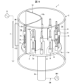
- FIG. 1 is a diagram illustrating a configuration of a main part of a plasma processing apparatus according to a first embodiment of the present disclosure.
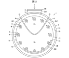
- 2 is a top view showing a configuration of a main part of the plasma processing apparatus.
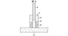
- FIG. 2A to 2C are diagrams illustrating an example of the configuration of a holder shown in FIG. 1 .
- 4 is a graph showing an example of the relationship between plasma electron density and sheath thickness in the plasma processing apparatus.
- 1A and 1B are diagrams illustrating an example of a relationship between a workpiece and a sheath in a film removal process.
- 2 is a diagram for explaining the shielding plate shown in FIG. 1 and the plasma processing region and cooling region formed thereby in the plasma processing apparatus.
- FIG. 1 is a diagram illustrating a configuration of a main part of a plasma processing apparatus according to a first embodiment of the present disclosure.
- FIG. 2 is a top view showing a configuration of a main part of the plasma processing apparatus.
- FIG. 11 is a top view showing a configuration of a main part of a plasma processing apparatus according to a second embodiment of the present disclosure.
- FIG. 11 is a diagram illustrating a configuration of a main part of a plasma processing apparatus according to a third embodiment of the present disclosure.
- FIG. 13 is a diagram illustrating a configuration of a main part of a plasma processing apparatus according to a fourth embodiment of the present disclosure.
- Fig. 1 is a diagram illustrating the configuration of the main parts of a plasma processing apparatus 1 according to the first embodiment of the present disclosure.
- Fig. 2 is a top view illustrating the configuration of the main parts of the plasma processing apparatus 1.
- Fig. 3 is a diagram illustrating an example of the configuration of a holder H shown in Fig. 1.
- a plasma processing device 1 that uses inductively coupled plasma as a specific plasma treatment to perform a film removal process that removes a coating from the surface of a workpiece W as a processing object in order to regenerate the surface of the workpiece W.
- the present disclosure can be applied to a plasma processing apparatus that performs, as a specified plasma treatment, a metal surface treatment such as carburizing, nitriding, ashing, or etching on the surface of the workpiece W.
- a plasma processing apparatus that performs, as a specified plasma treatment, a film formation treatment in which a specified coating is formed on the surface of the workpiece W by a plasma CVD (Chemical Vapor Deposition) method or a sputtering method.
- a plasma CVD Chemical Vapor Deposition
- the plasma processing apparatus 1 of the present embodiment 1 includes a vacuum vessel 2, a turntable 3, a shielding plate 4, a high-frequency window WR, and an antenna 7.
- the plasma processing apparatus 1 also includes a cooling mechanism CM and an application mechanism SM.
- the workpiece W is carried in and out of the vacuum vessel 2 through a door provided in the vacuum vessel 2 by a transport mechanism (not shown).
- the vacuum vessel 2 may be opened and the workpieces W may be replaced one by one or for each turntable 3.
- the workpiece W may be, for example, a drill for metal processing made of a metal material such as tungsten carbide or high-speed tool steel.
- the workpiece W may also be a tool other than a drill, for example, an end mill, a mold, or a special tool, or a special part for an automobile or an aircraft.
- the plasma processing device 1 removes a coating, such as a diamond-like carbon film, that has been formed on the surface of the workpiece W by the above-mentioned specified plasma processing.
- the vacuum vessel 2 is made of, for example, a metal material, and includes a vessel body 2a for forming a processing chamber in which the above-mentioned predetermined plasma processing is performed on the workpiece W.
- the vessel body 2a is, for example, cylindrical in shape, as shown in Figures 1 and 2.
- An upper lid and a lower lid (not shown) are airtightly attached to the upper and lower openings of the vessel body 2a, and the vacuum vessel 2 is configured to be brought to a predetermined vacuum level by a vacuum pump (not shown) with the workpiece W accommodated therein.
- the vacuum vessel 2 is grounded via a grounding wire (not shown), and a predetermined processing gas such as argon can be introduced into the vacuum vessel 2 as appropriate.
- the turntable 3 is made of, for example, a metal material, and includes a disk-shaped table body 3a and a rotating shaft 3b provided at the center of the table body 3a.
- the turntable 3 also forms a path for applying a predetermined bias voltage by an application mechanism SM, and applies the bias voltage to the workpiece W.
- the rotating shaft 3b is rotatably and airtightly attached to the lower lid of the vacuum vessel 2, and a driving mechanism (not shown) is connected to the rotating shaft 3b.
- the rotating shaft 3b rotates in the R1 direction shown in FIG. 1, so that the table body 3a revolves (rotates) in the R1 direction inside the vacuum vessel 2.
- the table body 3a is provided with, for example, multiple holders H that support the workpieces W, and a predetermined plasma treatment is sequentially performed on the workpieces W inside the plasma treatment area PA described below.
- the table body 3a rotates at a predetermined rotation speed (for example, 10 rpm), and the film removal treatment on each workpiece W is completed, for example, by the table body 3a rotating several times.
- the diameter of the table body 3a is as close as possible to the inner diameter of the container body 2a, in order to make effective use of the high-density plasma inside the plasma treatment area PA.
- the shielding plate 4 is made of a conductive material such as a metal material, and is provided inside the vacuum vessel 2 above the turntable 3 and facing the high frequency window WR. As shown in FIG. 2, the shielding plate 4 has a shielding plate body 4a formed in a V-shape when viewed from above. As shown in FIG. 6, the shielding plate body 4a is provided inside the vessel body 2a of the vacuum vessel 2 symmetrically with respect to the center and with each end of the shielding plate body 4a opening at a predetermined angle with respect to the center.
- the shielding plate body 4a shields the space between the high frequency window WR and the shielding plate 4, and the space functions as a plasma processing area PA where the above-mentioned predetermined plasma processing is performed on the workpiece W.
- the shielding plate 4 is configured to confine the plasma generated by the high frequency magnetic field from the high frequency window WR to the inside of the plasma processing area PA as much as possible by the shielding plate body 4a. That is, the shielding plate 4 has the function of shielding the plasma and dividing the inside of the vacuum chamber 2 into a plasma processing area PA and a cooling area CA, which will be described later.
- the shielding plate body 4a has through holes 4b1 and 4b2 that allow the workpiece W placed on the turntable 3 and the holder H supporting it to pass through. As a result, when the table body 3a revolves, the workpiece W and the holder H can pass through the through holes 4b1 and 4b2 to enter and exit the plasma processing area PA.
- the potential of the shielding plate body 4a is floating. Specifically, the left and right ends of the shielding plate body 4a are attached to the inner wall surface 2b of the container body 2a via insulators 4c ( Figure 2) made of a dielectric material. As a result, even when the shielding plate 4 confines plasma in the plasma processing area PA, the shielding plate body 4a can be charged to the plasma potential because the shielding plate 4 is not grounded. As a result, the shielding plate 4 can efficiently confine plasma in the plasma processing area PA while suppressing loss of plasma in the shielding plate body 4a, and the electron density of the plasma can be increased.
- the shielding plate body 4a may be attached to the upper lid of the vacuum vessel 2.
- the shielding plate 4 may also be made of a dielectric material such as glass. In this case, the installation of the insulator 4c may be omitted.
- the high frequency window WR includes a metal plate 5 and a dielectric plate 6, and is configured to introduce a high frequency magnetic field for generating plasma inside the vessel body 2a of the vacuum vessel 2 into the vessel body 2a.
- the metal plate 5 is provided with a plurality of slits, and the metal plate 5 is attached to the vessel body 2a so as to close the opening 2b1 provided in the inner wall surface 2b of the vessel body 2a.
- the dielectric plate 6 is attached to the metal plate 5 so as to cover at least the slits.
- the antenna 7 is, for example, linear and made of a metal material such as copper.
- the antenna 7 is provided vertically outside the container body 2a so as to face the high-frequency window WR.
- the antenna 7 generates a high-frequency magnetic field using high-frequency power from a power source 8, and introduces the high-frequency magnetic field into the container body 2a through the high-frequency window WR.
- one end of the antenna 7 is electrically connected to the power supply 8 via an impedance adjustment unit (not shown) having a matching circuit.
- the other end of the antenna 7 is electrically grounded via a variable capacitor (not shown).
- the power supply 8 supplies high-frequency power of, for example, 13.56 MHz to one end of the antenna 7 via the impedance adjustment unit.
- a control unit (not shown) changes the capacitance of the variable capacitor to control the efficient supply of high-frequency power to the antenna 7.
- the cooling mechanism CM is installed in a cooling area CA provided inside the container body 2a.
- the cooling area CA is the space inside the container body 2a separated by the shielding plate 4, excluding the plasma processing area PA.
- the cooling area CA is the area inside the container body 2a on the opposite side of the shielding plate 4 from the antenna 7.
- the cooling mechanism CM also includes a cooling plate CM1 arranged in the cooling area CA, and is configured to cool the workpiece W using the cooling plate CM1.
- the cooling mechanism CM includes a cooling plate CM1 formed in an arc shape using a metal material, and a pipe CM2 provided on the inner wall surface 2b side of the container body 2a of the cooling plate CM1 for circulating a cooling medium such as water.
- the surface of the cooling plate CM1 is provided inside the container body 2a so as to contact the holder H.
- the cooling plate CM1 cools the workpiece W by contacting the holder H without directly contacting the workpiece W, so that the workpiece W can be reliably cooled without being damaged.
- the application mechanism SM includes a power source SM1 provided outside the container body 2a, and applies a predetermined bias voltage from the power source SM1 to the workpiece W via the turntable 3.
- the workpiece W is subjected to a predetermined plasma processing in the plasma processing area PA while the bias voltage from the application mechanism SM is applied to the workpiece W.
- the power source SM1 is configured using, for example, a DC power source, a pulse power source, or an AC power source.
- the control unit is configured to change the bias voltage from the power source SM1 depending on the content of the plasma processing on the workpiece W and the electron density of the plasma in the plasma processing area PA, so that the plasma processing is performed appropriately.
- the application mechanism SM also has a number of holders H that are provided at predetermined intervals along the circumference of the table body 3a of the turntable 3.
- Each of the multiple holders H is for holding a workpiece W on the table body 3a, and in this embodiment 1, as described above, the table body 3a revolves, allowing the predetermined plasma processing to be performed sequentially on the multiple workpieces W.
- the holder H includes cylindrical support members H1 and H2 and a columnar application member H3.
- the support members H1 and H2 are made of, for example, a dielectric material.
- the support member H2 and application member H3 are provided on the table body 3a of the turntable 3.
- the support member H1 is supported rotatably by the support member H2, application member H3, and table body 3a.
- the application member H3 is electrically connected to the table body 3a and the workpiece W supported by the support member H1, and applies the bias voltage to the workpiece W supported by the support member H1.
- the support member H1 is configured to come into contact with the cooling plate CM1.
- the support member H1 comes into contact with the cooling plate CM1 as the table body 3a revolves, and the support member H1 (holder H) rotates (spins) in the R2 direction shown in FIG. 2.
- the support member H1 holder H
- spins spins
- the opposing surface of the workpiece W with respect to the high-frequency window WR can be changed in accordance with the spin. Therefore, in this embodiment 1, it is possible to reliably perform more uniform processing on the workpiece W.
- the plasma processing apparatus 1 of the present embodiment 1 configured as described above includes a vacuum vessel 2 that houses a workpiece W therein, a high-frequency window WR that introduces a high-frequency magnetic field into the vacuum vessel 2, and an antenna 7 that is disposed opposite the high-frequency window WR and generates a high-frequency magnetic field.
- the plasma processing apparatus 1 also includes a turntable 3 on which the workpiece W is placed and rotates, and an application mechanism SM that applies a predetermined bias voltage from a power source SM1 to the workpiece W via the turntable 3.
- the plasma processing apparatus 1 includes a shielding plate 4 that is disposed above the turntable 3 and inside the vacuum vessel 2 opposite the high-frequency window WR, shielding the space between the turntable 3 and the high-frequency window WR, and has through holes 4b1 and 4b2 formed in the shielding plate 4 that allow the workpiece W placed on the turntable 3 to pass through.
- a plasma processing apparatus 1 capable of efficiently processing the workpieces W can be configured.
- the inside of the vacuum vessel 2 is divided into plasma processing areas PA by the shielding plate 4, so that the electron density of the plasma in the plasma processing area PA can be increased, and the film removal rate (processing rate) for the workpieces W can be increased.
- the workpieces W can be efficiently processed.
- a single plasma source having one antenna 7 and one high-frequency window WR can be used to sequentially perform a predetermined plasma processing on multiple workpieces W.
- a low-cost plasma processing apparatus 1 capable of performing plasma processing on multiple workpieces W can be configured.
- Fig. 4 is a graph showing an example of the relationship between plasma electron density and sheath thickness in the plasma processing apparatus 1.
- Fig. 5 is a diagram explaining an example of the relationship between the workpiece W and the sheath SA in a film removal process.
- Fig. 6 is a diagram explaining the shielding plate 4 shown in Fig. 1, and the plasma processing area PA and cooling area CA formed thereby in the plasma processing apparatus 1.
- Fig. 7 is a graph showing an example of the relationship between the rotation angle of the turntable 3 shown in Fig. 1 and the plasma electron density. Note that the power supply 8, power supply SM1, and piping CM2 are not shown in Fig. 6.
- the sheath thickness of the sheath SA (FIG. 5) generated around the workpiece W in the plasma processing area PA changes according to the plasma electron density for each bias voltage.
- the sheath SA is a shielding layer that is generated to surround the workpiece W by the bias voltage and prevents the plasma ions from approaching the workpiece W.
- the sheath thickness changes according to the plasma electron density, as shown by curve 71 in FIG. 4.
- the bias voltage is, for example, -250V
- the sheath thickness changes according to the plasma electron density, as shown by curve 72 in FIG. 4.
- the bias voltage is, for example, -500V
- the sheath thickness changes according to the plasma electron density, as shown by curve 73 in FIG. 4.
- the sheath thickness around the workpiece W in a cross-sectional view of the workpiece W varies depending on the plasma electron density, as shown in 502 and 503 in FIG. 5.
- the plasma electron density is low
- the thickness of the sheath SA becomes large, as shown in 502 in FIG. 5. Therefore, the plasma ions P1 are prevented from approaching the surface of the workpiece W by the relatively thick sheath SA.
- the plasma electron density is low and the sheath thickness is large, it becomes difficult to perform a uniform film removal process on the workpiece W.
- the thickness of the sheath SA can be made smaller, as shown in 503 in FIG. 5, than that shown in 502 in FIG. 5. Therefore, in the plasma processing apparatus 1 of this embodiment 1, the relatively thin sheath SA prevents the plasma ions P1 from approaching the surface of the workpiece W. In other words, in the plasma processing apparatus 1 of this embodiment 1, the plasma ions P1 can more easily approach the surface of the workpiece W, allowing for uniform film removal processing.
- the inside of the vessel body 2a of the vacuum vessel 2 is divided by the shielding plate 4 into a plasma processing area PA on the plasma source side and a cooling area CA on the opposite side of the plasma source.
- the shielding plate 4 is installed inside the vessel body 2a so that the center of the shielding plate body 4a is, for example, on the center C1 of the rotation axis 3b of the turntable 3.
- the shielding plate body 4a has an opening angle of its left and right ends, and the above-mentioned predetermined angle ⁇ is set to, for example, 120°.
- the plasma processing area PA in which the electron density of the plasma is increased by the shielding plate 4 and the cooling area CA in which the plasma processing on the workpiece W is temporarily stopped and the temperature rise in the workpiece W due to the execution of the plasma processing can be appropriately formed by substantially shielding the plasma source with the shielding plate 4 and suppressing the spread of the plasma.
- the above-mentioned predetermined plasma processing can be performed more efficiently in the plasma processing area PA.
- the plasma electron density in the plasma processing area PA can be set to a value greater than the reference electron density, as shown by the upward arrow in Fig. 7.
- the rotation angle on the horizontal axis in Fig. 7 is the rotation angle of the turntable 3 with respect to the center C1, and is set to 0° when any reference position of the turntable 3 faces the antenna 7.
- the plasma electron density can be set to a value smaller than the reference electron density.
- the execution of plasma processing is suppressed, so that the temperature rise in the workpiece W due to the plasma processing can be suppressed, and the temperature of the workpiece W can be easily lowered.
- the temperature rise in the workpiece W can be significantly suppressed.
- the occurrence of damage, etc., in the workpiece W can be significantly reduced.
- the shielding plate 4 is arranged inside the container body 2a so that the center of the shielding plate body 4a is located on the center C1 of the rotation axis 3b of the turntable 3.
- this embodiment is not limited to this, and for example, the center of the shielding plate body 4a may be arranged closer to the high frequency window WR than the center C1. This is preferable because it allows the electron density of the plasma to be increased.
- Fig. 8 is a top view showing a main configuration of a plasma processing apparatus 1 according to the second embodiment of the present disclosure.
- the same reference numerals are used for members having the same functions as those described in the first embodiment, and the explanations thereof will not be repeated.
- the power source 8 the power source SM1, and the piping CM2 are not shown.
- a contact member 2c is provided on the inner wall surface 2b of the vacuum vessel 2.
- This contact member 2c is, for example, made of a metal material and has a rod-like shape.
- One end of the contact member 2c is attached to the inner wall surface 2b so as to protrude from the inner wall surface 2b into the inside of the vessel body 2a.
- the other end (protruding end) of the contact member 2c is configured so as to be able to come into contact with the support member H1 of the holder H.
- the plasma processing apparatus 1 of this embodiment 2 achieves the same effects as that of embodiment 1.
- the support member H1 of the holder H is rotated by contact with the contact member 2c, so that more uniform processing of the workpiece W can be performed more reliably.
- the support member H1 may be rotated only by contact with the contact member 2c.
- the support member H1 of the holder H is rotated by contact with the cooling plate CM1 and/or the contact member 2c.
- this embodiment is not limited to this, and for example, a rotation mechanism such as a gear may be provided that is connected to the holder H and rotates the support member H1 of the holder H using a rotational force from a drive mechanism that drives the rotation shaft 3b of the turntable 3.
- Fig. 9 is a diagram for explaining the main configuration of a plasma processing apparatus 1 according to the third embodiment of the present disclosure.
- the same reference numerals are given to members having the same functions as those described in the first embodiment, and the explanations thereof will not be repeated.
- the cooling mechanism CM is omitted.
- multiple groups of holders H for example, two rows, are provided, each arranged in an arc along the extension direction of the antenna 7.
- the lower vertical group of holders H is attached to the table body 3a of the turntable 3, as in the embodiment 1.
- the upper vertical group of holders H is attached to the table body 3a via a support rod 15, one end of which is provided on the table body 3a.
- the support rod 15 is adapted to rotatably support a support member H1 that supports the workpiece W.
- the inside of the vessel body 2a is divided into a plasma processing area PA and a cooling area CA by a shielding plate 14 having a shielding plate body 14a.
- the shielding plate 14 is provided with a passing hole 14b1 that allows the vertically upper and lower groups of holders H to pass through.
- the plasma processing apparatus 1 of this embodiment 3 achieves the same effects as that of embodiment 1.
- the workpieces W are supported by two rows of holders H along the extension direction of the antenna 7, so the number of workpieces W processed per unit time can be easily increased.
- Fig. 10 is a diagram for explaining the configuration of the main parts of a plasma processing apparatus 1 according to the fourth embodiment of the present disclosure.
- Fig. 10 is a diagram for explaining the configuration of the main parts of a plasma processing apparatus 1 according to the fourth embodiment of the present disclosure.
- the same reference numerals are given to members having the same functions as those explained in the first embodiment, and the explanations thereof will not be repeated.
- a cylindrical workpiece W0 is placed on the table body 3a of the turntable 3.
- the workpiece W0 is placed above the rotation axis 3b, which is the center of rotation of the turntable 3.
- the inside of the container body 2a is divided into a plasma processing area PA and a cooling area CA by a shielding plate 24 having a shielding plate body 24a.
- the shielding plate 24 is provided with a through hole 24b that allows the workpiece W0, which rotates with the rotation of the turntable 3, to pass through.
- the opposing surface of the workpiece W0 with respect to the high-frequency window WR can be changed according to the rotation of the turntable 3.
- a part of the workpiece W0 can be moved sequentially between the plasma processing area PA and the cooling area CA.
- the plasma processing apparatus 1 of this embodiment 4 achieves the same effects as that of embodiment 1.
- the plasma processing apparatus of the first aspect of the present disclosure comprises a vacuum vessel for accommodating a workpiece therein, a high-frequency window for introducing a high-frequency magnetic field into the vacuum vessel to generate plasma inside the vacuum vessel, an antenna arranged outside the vacuum vessel facing the high-frequency window and generating the high-frequency magnetic field, a turntable on which the workpiece is placed and which rotates inside the vacuum vessel, and a shielding plate arranged inside the vacuum vessel above the turntable and facing the high-frequency window, shielding from plasma and dividing the inside of the vacuum vessel into a plasma processing region and a cooling region, the shielding plate having a passage hole formed therein to allow the workpiece placed on the turntable to pass through.
- the above configuration makes it possible to provide a plasma processing apparatus that can efficiently process the workpiece.
- the shielding plate when viewed from the top of the vacuum vessel, may be provided inside the vacuum vessel so that it is symmetrical with respect to its center and that each of the left and right ends opens at a predetermined angle with respect to the center.
- the shielding plate can appropriately form a plasma processing area inside the vacuum vessel, allowing plasma processing to be performed more efficiently.
- the potential of the shielding plate may be floating.
- the above configuration makes it possible to prevent plasma loss and maintain a higher plasma density.
- a fourth aspect of the present disclosure is a plasma processing apparatus according to any one of the first to third aspects, further comprising an application mechanism that includes a power source provided outside the vacuum vessel and applies a predetermined bias voltage from the power source to the workpiece via the turntable, and the application mechanism has a holder provided on the turntable to hold the workpiece, the holder being provided on the turntable and including a support member that rotatably supports the workpiece, and an application member that is electrically connected to the turntable and the workpiece supported by the support member and applies the bias voltage to the workpiece supported by the support member.
- a fifth aspect of the present disclosure is the plasma processing apparatus of the fourth aspect, in which a contact member may be provided inside the vacuum vessel to come into contact with the support member of the holder and rotate the support member in response to the rotation of the turntable.
- the above configuration makes it possible to more reliably perform more uniform processing on the workpiece.
- a sixth aspect of the present disclosure is a plasma processing apparatus according to either the fourth or fifth aspect, which may include a cooling plate disposed inside the vacuum vessel in an area of the shielding plate opposite the antenna, and a cooling mechanism that uses the cooling plate to cool the workpiece.
- the above configuration allows the workpiece to be cooled more quickly, resulting in a faster processing rate.
- the cooling plate may be in contact with the holder.
- the above configuration ensures that the workpiece can be cooled without damaging it.
- a plurality of the objects to be processed may be provided inside the vacuum vessel along the extension direction of the antenna.
- the above configuration makes it easy to increase the number of objects processed per unit time.
- Plasma processing apparatus Vacuum vessel 2c Contact member 3 Turntable 3b Rotating shaft 4, 14, 24 Shielding plate 4b1, 4b2, 14b1, 24b Passing hole 5 Metal plate (high frequency window) 6. Dielectric plate (high frequency window) 7 Antenna W, W0 Work (processing object)
- SM Voltage application mechanism SM1: Power supply H: Holder H1, H2: Support member H3: Voltage application member CM: Cooling mechanism CM1: Cooling plate WR: High frequency window PA: Plasma processing area CA: Cooling area
Landscapes
- Physics & Mathematics (AREA)
- Engineering & Computer Science (AREA)
- Chemical & Material Sciences (AREA)
- Plasma & Fusion (AREA)
- Materials Engineering (AREA)
- Chemical Kinetics & Catalysis (AREA)
- General Chemical & Material Sciences (AREA)
- Mechanical Engineering (AREA)
- Metallurgy (AREA)
- Organic Chemistry (AREA)
- Electromagnetism (AREA)
- Spectroscopy & Molecular Physics (AREA)
- Plasma Technology (AREA)
Abstract
Description
以下、本開示の実施形態1について、図1乃至図3を用いて詳細に説明する。図1は、本開示の実施形態1に係るプラズマ処理装置1の要部構成を説明する図である。図2は、上記プラズマ処理装置1の要部構成を示す上面図である。図3は、図1に示したホルダーHの構成例を説明する図である。
図1に示すように、本実施形態1のプラズマ処理装置1は、真空容器2と、ターンテーブル3と、遮蔽板4と、高周波窓WRと、アンテナ7と、を備えている。また、プラズマ処理装置1は、冷却機構CMと、印加機構SMと、を備えている。さらに、プラズマ処理装置1では、ワークWは、例えば、搬送機構によって真空容器2に設けられた扉を通して真空容器2の内部に搬入出される(図示せず)。なお、この説明以外に、真空容器2を開放して、ワークWを1個ずつ、あるいはターンテーブル3ごとにワークWを交換する構成でもよい。
真空容器2は、例えば、金属材料を用いて構成されており、ワークWに対して上記所定のプラズマ処理を行う処理室を構成するための容器本体2aを備えている。また、容器本体2aは、図1及び図2に示すように、例えば、円筒形の形状に構成されている。さらに、容器本体2aの上側開口及び下側開口には、図示しない上蓋及び下蓋が気密に取り付けられるようになっており、真空容器2はワークWを内部に収容した状態で、図示しない真空ポンプによって所定の真空度とされるように構成されている。また、真空容器2は、図示しない接地線を介して接地されるとともに、真空容器2の内部には、アルゴンなどの所定の処理ガスが適宜導入され得る。
ターンテーブル3は、例えば、金属材料を用いて構成されており、円板状のテーブル本体3aと、テーブル本体3aの中央部に設けられた回転軸3bと、を備えている。また、ターンテーブル3は、印加機構SMによる所定のバイアス電圧の印加経路を構成しており、当該バイアス電圧をワークWに印加するようになっている。また、ターンテーブル3では、回転軸3bは回動可能に真空容器2の上記下蓋に気密に取り付けられ、かつ、回転軸3bには図示しない駆動機構が連結されている。そして、ターンテーブル3では、回転軸3bが図1に示すR1方向に回動することにより、テーブル本体3aは、真空容器2の内部でR1方向に公転(回転)するよう構成されている。
遮蔽板4は、例えば、金属材料などの導電性材料を用いて構成されており、ターンテーブル3の上方、かつ、高周波窓WRに対向するように真空容器2の内部に設けられている。遮蔽板4は、図2に示すように、上面視でV字状に形成された遮蔽板本体4aを備えている。遮蔽板本体4aには、後掲の図6に示すように、その中央部に対して左右対称に、かつ、当該中央部を中心にして左右の各端部が所定の角度で開くように真空容器2の容器本体2aの内部に設けられている。そして、遮蔽板4では、遮蔽板本体4aが高周波窓WRとの間の空間を遮蔽して、当該空間をワークWに対する上記所定のプラズマ処理が実行されるプラズマ処理領域PAとして機能させるようになっている。換言すれば、遮蔽板4は、遮蔽板本体4aによって高周波窓WRからの高周波磁場によって発生するプラズマをプラズマ処理領域PAの内部に極力閉じ込めるように構成されている。すなわち、遮蔽板4は、プラズマを遮蔽して、真空容器2の内部をプラズマ処理領域PAと後述の冷却領域CAとに分割する機能を有する。
高周波窓WRは、金属板5と、誘電体板6と、を備えており、真空容器2の容器本体2aの内部にプラズマを発生させる高周波磁場を、容器本体2aの内部に導入させるように構成されている。具体的にいえば、金属板5には、複数のスリットが設けられており、金属板5は、容器本体2aの内壁面2bに設けられた開口部2b1を塞ぐように容器本体2aに取り付けられている。また、誘電体板6は、少なくとも上記スリットを覆うように金属板5に取り付けられている。
アンテナ7は、例えば、直線状に構成されるとともに、銅などの金属材料を用いて構成されている。また、アンテナ7は、鉛直方向に沿って容器本体2aの外側で高周波窓WRに対向するように設けられている。さらに、アンテナ7は、電源8からの高周波電力により、高周波磁場を発生して、高周波窓WRを介して容器本体2aの内部に高周波磁場を導入する。
冷却機構CMは、容器本体2aの内部に設けられた冷却領域CAに設置されている。冷却領域CAは、遮蔽板4によって区切られた容器本体2aの内部の空間のうち、プラズマ処理領域PAを除いた空間にて構成される。換言すれば、冷却領域CAは、容器本体2aの内部において、遮蔽板4のアンテナ7とは反対側の領域である。また、冷却機構CMは、冷却領域CAに配置された冷却板CM1を具備しており、冷却板CM1を用いてワークWを冷却するようになっている。
印加機構SMは、容器本体2aの外部に設けられた電源SM1を具備し、所定のバイアス電圧を電源SM1からターンテーブル3を介してワークWに印加する。換言すれば、プラズマ処理装置1では、ワークWは印加機構SMからのバイアス電圧が印加された状態でプラズマ処理領域PAの内部で所定のプラズマ処理が施される。また、電源SM1は、例えば、直流電源、パルス電源、または交流電源を用いて構成されている。印加機構SMでは、ワークWに対するプラズマ処理の内容及びプラズマ処理領域PAでのプラズマの電子密度などに応じて、上記制御部が電源SM1からのバイアス電圧を変更するよう構成されており、プラズマ処理を適切に行うようになっている。
本開示の実施形態2について、図8を用いて具体的に説明する。図8は、本開示の実施形態2に係るプラズマ処理装置1の要部構成を示す上面図である。なお、説明の便宜上、上記実施形態1にて説明した部材と同じ機能を有する部材については、同じ符号を付記し、その説明を繰り返さない。また、図8では、電源8、電源SM1、及び配管CM2の図示は省略している。
本開示の実施形態3について、図9を用いて具体的に説明する。図9は、本開示の実施形態3に係るプラズマ処理装置1の要部構成を説明する図である。なお、説明の便宜上、上記実施形態1にて説明した部材と同じ機能を有する部材については、同じ符号を付記し、その説明を繰り返さない。なお、図9では、冷却機構CMの図示は省略している。
本開示の実施形態4について、図10を用いて具体的に説明する。図10は、本開示の実施形態4に係るプラズマ処理装置1の要部構成を説明する図である。なお、説明の便宜上、上記実施形態1にて説明した部材と同じ機能を有する部材については、同じ符号を付記し、その説明を繰り返さない。
上記の課題を解決するために、本開示の第1態様のプラズマ処理装置は、被処理物を内部に収容する真空容器と、前記真空容器の内部にプラズマを発生させる高周波磁場を、前記真空容器の内部に導入させる高周波窓と、前記真空容器の外側で前記高周波窓に対向するように設けられて、前記高周波磁場を発生するアンテナと、前記被処理物が載置されるとともに、前記真空容器の内部で回転するターンテーブルと、前記ターンテーブルの上方、かつ、前記高周波窓に対向するように前記真空容器の内部に設けられて、プラズマを遮蔽して、前記真空容器の内部をプラズマ処理領域と冷却領域とに分割する遮蔽板であって、前記ターンテーブル上に載置された前記被処理物が通過するのを許容する通過穴が形成されている遮蔽板と、を備えている。
2 真空容器
2c 接触部材
3 ターンテーブル
3b 回転軸
4、14、24 遮蔽板
4b1、4b2、14b1、24b 通過穴
5 金属板(高周波窓)
6 誘電体板(高周波窓)
7 アンテナ
W、W0 ワーク(被処理物)
SM 印加機構
SM1 電源
H ホルダー
H1、H2 支持部材
H3 印加部材
CM 冷却機構
CM1 冷却板
WR 高周波窓
PA プラズマ処理領域
CA 冷却領域
Claims (8)
- 被処理物を内部に収容する真空容器と、
前記真空容器の内部にプラズマを発生させる高周波磁場を、前記真空容器の内部に導入させる高周波窓と、
前記真空容器の外側で前記高周波窓に対向するように設けられて、前記高周波磁場を発生するアンテナと、
前記被処理物が載置されるとともに、前記真空容器の内部で回転するターンテーブルと、
前記ターンテーブルの上方、かつ、前記高周波窓に対向するように前記真空容器の内部に設けられて、プラズマを遮蔽して、前記真空容器の内部をプラズマ処理領域と冷却領域とに分割する遮蔽板であって、前記ターンテーブル上に載置された前記被処理物が通過するのを許容する通過穴が形成されている遮蔽板と、を備えている、プラズマ処理装置。 - 前記真空容器の上面から視認した場合、前記遮蔽板は、その中央部に対して左右対称に、かつ、当該中央部を中心にして左右の各端部が所定の角度で開くように前記真空容器の内部に設けられている、請求項1に記載のプラズマ処理装置。
- 前記遮蔽板の電位は、フローティングである、請求項1に記載のプラズマ処理装置。
- 前記真空容器の外部に設けられた電源を具備し、所定のバイアス電圧を当該電源から前記ターンテーブルを介して前記被処理物に印加する印加機構を、さらに備え、
前記印加機構は、
前記被処理物を保持するために前記ターンテーブルに設けられたホルダーを有し、
前記ホルダーは、
前記ターンテーブルに設けられるとともに、前記被処理物を回転自在に支持する支持部材と、
前記ターンテーブルと前記支持部材に支持された前記被処理物とに電気的に接続されて、前記支持部材に支持された前記被処理物に前記バイアス電圧を印加する印加部材と、を含む、請求項1に記載のプラズマ処理装置。 - 前記真空容器の内部には、前記ホルダーの前記支持部材に接触して、前記ターンテーブルの回転に応じて、前記支持部材を回転させる接触部材が設けられている、請求項4に記載のプラズマ処理装置。
- 前記真空容器の内部において、前記遮蔽板の前記アンテナとは反対側の領域に配置された冷却板を具備し、当該冷却板を用いて前記被処理物を冷却する冷却機構が設けられている、請求項4に記載のプラズマ処理装置。
- 前記冷却板は、前記ホルダーと接触する、請求項6に記載のプラズマ処理装置。
- 前記真空容器の内部には、複数の前記被処理物が、前記アンテナが延伸する延伸方向に沿って設けられている、請求項1から7のいずれか1項に記載のプラズマ処理装置。
Priority Applications (3)
| Application Number | Priority Date | Filing Date | Title |
|---|---|---|---|
| JP2024575993A JPWO2024166299A1 (ja) | 2023-02-09 | 2023-02-09 | |
| PCT/JP2023/004383 WO2024166299A1 (ja) | 2023-02-09 | 2023-02-09 | プラズマ処理装置 |
| CN202380081902.XA CN120283447A (zh) | 2023-02-09 | 2023-02-09 | 等离子体处理装置 |
Applications Claiming Priority (1)
| Application Number | Priority Date | Filing Date | Title |
|---|---|---|---|
| PCT/JP2023/004383 WO2024166299A1 (ja) | 2023-02-09 | 2023-02-09 | プラズマ処理装置 |
Publications (1)
| Publication Number | Publication Date |
|---|---|
| WO2024166299A1 true WO2024166299A1 (ja) | 2024-08-15 |
Family
ID=92262234
Family Applications (1)
| Application Number | Title | Priority Date | Filing Date |
|---|---|---|---|
| PCT/JP2023/004383 Ceased WO2024166299A1 (ja) | 2023-02-09 | 2023-02-09 | プラズマ処理装置 |
Country Status (3)
| Country | Link |
|---|---|
| JP (1) | JPWO2024166299A1 (ja) |
| CN (1) | CN120283447A (ja) |
| WO (1) | WO2024166299A1 (ja) |
Citations (8)
| Publication number | Priority date | Publication date | Assignee | Title |
|---|---|---|---|---|
| JPH0372077A (ja) * | 1989-08-10 | 1991-03-27 | Anelva Corp | Cvd方法 |
| JPH06204147A (ja) * | 1992-08-29 | 1994-07-22 | Tokyo Electron Ltd | 処理装置 |
| JP2006093543A (ja) * | 2004-09-27 | 2006-04-06 | Tokyo Electron Ltd | 熱処理装置 |
| JP2009205845A (ja) * | 2008-02-26 | 2009-09-10 | Nissin Ion Equipment Co Ltd | イオン源およびイオン注入装置 |
| JP2015074792A (ja) * | 2013-10-07 | 2015-04-20 | 株式会社Screenホールディングス | プラズマcvd装置 |
| JP2020132906A (ja) * | 2019-02-14 | 2020-08-31 | Towa株式会社 | 成膜品の製造方法及びスパッタリング装置 |
| JP2022180370A (ja) * | 2017-03-31 | 2022-12-06 | 芝浦メカトロニクス株式会社 | プラズマ処理装置 |
| JP2023004296A (ja) * | 2021-06-25 | 2023-01-17 | 日新電機株式会社 | 除膜装置 |
-
2023
- 2023-02-09 JP JP2024575993A patent/JPWO2024166299A1/ja active Pending
- 2023-02-09 WO PCT/JP2023/004383 patent/WO2024166299A1/ja not_active Ceased
- 2023-02-09 CN CN202380081902.XA patent/CN120283447A/zh active Pending
Patent Citations (8)
| Publication number | Priority date | Publication date | Assignee | Title |
|---|---|---|---|---|
| JPH0372077A (ja) * | 1989-08-10 | 1991-03-27 | Anelva Corp | Cvd方法 |
| JPH06204147A (ja) * | 1992-08-29 | 1994-07-22 | Tokyo Electron Ltd | 処理装置 |
| JP2006093543A (ja) * | 2004-09-27 | 2006-04-06 | Tokyo Electron Ltd | 熱処理装置 |
| JP2009205845A (ja) * | 2008-02-26 | 2009-09-10 | Nissin Ion Equipment Co Ltd | イオン源およびイオン注入装置 |
| JP2015074792A (ja) * | 2013-10-07 | 2015-04-20 | 株式会社Screenホールディングス | プラズマcvd装置 |
| JP2022180370A (ja) * | 2017-03-31 | 2022-12-06 | 芝浦メカトロニクス株式会社 | プラズマ処理装置 |
| JP2020132906A (ja) * | 2019-02-14 | 2020-08-31 | Towa株式会社 | 成膜品の製造方法及びスパッタリング装置 |
| JP2023004296A (ja) * | 2021-06-25 | 2023-01-17 | 日新電機株式会社 | 除膜装置 |
Also Published As
| Publication number | Publication date |
|---|---|
| CN120283447A (zh) | 2025-07-08 |
| JPWO2024166299A1 (ja) | 2024-08-15 |
Similar Documents
| Publication | Publication Date | Title |
|---|---|---|
| JP4812991B2 (ja) | プラズマ処理装置 | |
| JP6126302B2 (ja) | 成膜装置 | |
| US20050211383A1 (en) | Magnetron plasma-use magnetic field generation device | |
| KR102079595B1 (ko) | 멀티 회전식 플라즈마 발생장치 | |
| JP6595396B2 (ja) | プラズマ処理装置 | |
| KR100754370B1 (ko) | 향상된 중성입자 플럭스를 갖는 중성입자빔 생성장치 | |
| KR102371334B1 (ko) | 성막 방법 및 성막 장치 | |
| JP6955983B2 (ja) | 基板処理装置 | |
| KR102050631B1 (ko) | 기판에 형성된 오목부에 구리 배선을 형성하기 위한 전처리를 행하는 방법, 및 처리 장치 | |
| KR20180019201A (ko) | 진공 아크 성막 장치 및 성막 방법 | |
| JP2023004296A (ja) | 除膜装置 | |
| KR20210018645A (ko) | 기판 처리 장치 및 기판 처리 방법 | |
| US10541142B2 (en) | Maintenance method of plasma processing apparatus | |
| WO2024180578A1 (ja) | プラズマ処理装置 | |
| CN120283447A (zh) | 等离子体处理装置 | |
| JP4541014B2 (ja) | プラズマ支援スパッタ成膜装置 | |
| JP4437347B2 (ja) | 前処理エッチング装置及び薄膜作成装置 | |
| TW202135124A (zh) | 用於加工基材的設備 | |
| JP3180557U (ja) | 薄膜作製装置 | |
| JP5236777B2 (ja) | プラズマ処理装置 | |
| JP2025151560A (ja) | プラズマ処理装置及びプラズマ処理方法 | |
| KR102100402B1 (ko) | 플라즈마 공정장비의 하부캐소드 모듈 | |
| JP4135173B2 (ja) | プラズマ処理装置及びプラズマ処理方法 | |
| JP2023114815A (ja) | プラズマ処理装置 | |
| JP2871619B2 (ja) | ダイヤモンド様炭素薄膜堆積装置 |
Legal Events
| Date | Code | Title | Description |
|---|---|---|---|
| 121 | Ep: the epo has been informed by wipo that ep was designated in this application |
Ref document number: 23921130 Country of ref document: EP Kind code of ref document: A1 |
|
| WWE | Wipo information: entry into national phase |
Ref document number: 202380081902.X Country of ref document: CN |
|
| ENP | Entry into the national phase |
Ref document number: 2024575993 Country of ref document: JP Kind code of ref document: A |
|
| WWE | Wipo information: entry into national phase |
Ref document number: 2024575993 Country of ref document: JP |
|
| WWP | Wipo information: published in national office |
Ref document number: 202380081902.X Country of ref document: CN |
|
| NENP | Non-entry into the national phase |
Ref country code: DE |
|
| 122 | Ep: pct application non-entry in european phase |
Ref document number: 23921130 Country of ref document: EP Kind code of ref document: A1 |