WO2024162040A1 - 配線基板および実装構造体 - Google Patents
配線基板および実装構造体 Download PDFInfo
- Publication number
- WO2024162040A1 WO2024162040A1 PCT/JP2024/001451 JP2024001451W WO2024162040A1 WO 2024162040 A1 WO2024162040 A1 WO 2024162040A1 JP 2024001451 W JP2024001451 W JP 2024001451W WO 2024162040 A1 WO2024162040 A1 WO 2024162040A1
- Authority
- WO
- WIPO (PCT)
- Prior art keywords
- conductor
- groove
- recess
- insulating layer
- wiring board
- Prior art date
- Legal status (The legal status is an assumption and is not a legal conclusion. Google has not performed a legal analysis and makes no representation as to the accuracy of the status listed.)
- Ceased
Links
Images



Classifications
-
- H—ELECTRICITY
- H05—ELECTRIC TECHNIQUES NOT OTHERWISE PROVIDED FOR
- H05K—PRINTED CIRCUITS; CASINGS OR CONSTRUCTIONAL DETAILS OF ELECTRIC APPARATUS; MANUFACTURE OF ASSEMBLAGES OF ELECTRICAL COMPONENTS
- H05K1/00—Printed circuits
- H05K1/02—Details
-
- H—ELECTRICITY
- H05—ELECTRIC TECHNIQUES NOT OTHERWISE PROVIDED FOR
- H05K—PRINTED CIRCUITS; CASINGS OR CONSTRUCTIONAL DETAILS OF ELECTRIC APPARATUS; MANUFACTURE OF ASSEMBLAGES OF ELECTRICAL COMPONENTS
- H05K3/00—Apparatus or processes for manufacturing printed circuits
- H05K3/46—Manufacturing multilayer circuits
Definitions
- the present invention relates to a wiring board and a mounting structure using the same.
- Patent Document 1 wiring patterns formed on wiring boards are formed with fine wiring at high density in line with the miniaturization of electronic devices.
- width between the wiring becomes narrower due to finer wiring, short circuits due to ion migration become more likely to occur.
- Patent Document 2 provides a recess between adjacent conductors, with the deepest part being the midpoint between the adjacent conductors.
- the wiring board according to the present disclosure includes a first insulating layer having a first surface, a first conductor located on the first surface, a second conductor located adjacent to the first conductor on the first surface, a first groove located between the first conductor and the second conductor on the first surface, and a second insulating layer located on the first surface, covering the first conductor and the second conductor, and embedded in the first groove.
- the first groove includes a first recess located on the first conductor side and recessed on the opposite side to the first surface, a second recess located on the second conductor side and recessed on the opposite side to the first surface, and a first intermediate portion located between the first recess and the second recess and having an end portion closer to the first surface than the bottom of the first recess and the bottom of the second recess.
- the mounting structure according to the present disclosure includes the above-mentioned wiring board and an electronic component mounted on the wiring board.
- FIG. 2 is an explanatory diagram for explaining a wiring board according to an embodiment of the present disclosure.
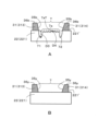
- 2A is an enlarged explanatory view for explaining one embodiment of a cross section of region X shown in FIG. 1 (cross section including the first groove)
- FIG. 2B is an enlarged explanatory view for explaining one embodiment of a portion of region X shown in FIG. 1 that differs from FIG. 2A (cross section not including the first groove)
- FIG. 2C is a plan view seen from the direction of arrow A shown in FIG. 2A (however, the second insulating layer is omitted).
- 3A is an enlarged explanatory diagram for illustrating another embodiment of the cross section of region X shown in FIG. 1, and FIG.
- 3B is a plan view seen from the direction of arrow B shown in FIG. 3A (however, the second insulating layer is omitted).
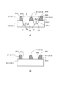
- 4A is an enlarged explanatory view for explaining another embodiment of the cross section of region X shown in FIG. 1 (cross section including the second groove), and
- FIG. 4B is an enlarged explanatory view for explaining another embodiment of a portion of region X shown in FIG. 1 that differs from FIG. 4A (cross section not including the second groove).
- 5A is an enlarged explanatory view for explaining another embodiment of the cross section of region X shown in FIG. 1 (a cross section including the first groove and the third groove), and
- FIG. 5B is an enlarged explanatory view for explaining another embodiment of a portion of region X shown in FIG.
- FIG. 6 is a graph showing the unevenness of the first side surface based on the results of measuring the first side surface using a three-dimensional white light interference microscope.
- FIG. 7 is a graph showing the unevenness of the side surfaces other than the first side surface based on the results of measuring the side surfaces other than the first side surface using a three-dimensional white light interference microscope.
- FIG. 8 is a graph showing the unevenness of the first upper surface based on the results of measuring the first upper surface using a three-dimensional white light interference microscope.
- FIG. 9 is a graph showing the unevenness of the top surface other than the first top surface based on the result of measuring the top surface other than the first top surface using a three-dimensional white light interference microscope.
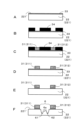
- 10A to 10C are explanatory views for explaining one embodiment of a method for forming a first recess, a second recess, and a first intermediate portion in a first groove.
- 10A to 10C are explanatory views for explaining another embodiment of a method for forming a first recess, a second recess, and a first intermediate portion in a first groove.
- the wiring board according to the present disclosure has a configuration as described in the section on means for solving the above problems, thereby reducing short circuits caused by ion migration and providing high insulation reliability.
- FIG. 1 is an explanatory diagram for explaining a wiring board 1 according to an embodiment of the present disclosure.
- the wiring board 1 according to the embodiment includes an insulating layer 2, a conductor layer 3, and a solder resist 4.
- the insulating layer 2 includes a core insulating layer 21 and a build-up insulating layer 22.
- the core insulating layer 21 is not particularly limited as long as it is made of an insulating material. Examples of insulating materials include resins such as epoxy resin, bismaleimide-triazine resin, polyimide resin, and polyphenylene ether resin. Only one of these resins may be used, or two or more of them may be used in combination.
- the thickness of the core insulating layer 21 is not particularly limited, and is, for example, 0.04 mm or more and 2 mm or less.
- the core insulating layer 21 may contain a reinforcing material.
- reinforcing materials include insulating cloth materials such as glass fiber, glass nonwoven fabric, aramid nonwoven fabric, aramid fiber, and polyester fiber. Only one type of reinforcing material may be used, or two or more types may be used in combination.
- the core insulating layer 21 may have inorganic insulating fillers such as silica, barium sulfate, talc, clay, glass, calcium carbonate, and titanium oxide dispersed therein. Only one type of inorganic filler may be used, or two or more types may be used in combination.
- Through-hole conductors 21a are located in the core insulating layer 21 to electrically connect the top and bottom surfaces of the core insulating layer 21.
- the through-hole conductors 21a are located in through-holes that penetrate the core insulating layer 21 from the top surface to the bottom surface.
- the through-hole conductors 21a are formed, for example, by metal plating such as copper plating.
- the through-hole conductors 21a are connected to the conductor layers 3 located on both sides of the core insulating layer 21.
- the through-hole conductors 21a may be located only on the inner surface of the through-hole, or may be filled in the through-hole.
- the upper and lower surfaces of the core insulating layer 21 are provided with a build-up layer in which conductor layers 3 and build-up insulating layers 22 are alternately stacked.
- the conductor layer 3 is not limited as long as it is a conductor such as a metal.
- the conductor layer 3 is formed of a metal foil such as copper foil, a metal plating such as copper plating, or the like.
- the thickness of the conductor layer 3 is not particularly limited, and is, for example, 5 ⁇ m or more and 25 ⁇ m or less.
- the build-up insulating layer 22, like the core insulating layer 21, is not particularly limited as long as it is made of an insulating material.
- insulating materials include resins such as epoxy resin, bismaleimide-triazine resin, polyimide resin, and polyphenylene ether resin. Only one type of these resins may be used, or two or more types may be used in combination.
- the build-up insulating layers 22 may be made of the same resin or different resins.
- the build-up insulating layer 22 and the core insulating layer 21 may be made of the same resin or different resins.
- the build-up insulating layer 22 may contain a reinforcing material.
- reinforcing materials include insulating cloth materials such as glass fiber, glass nonwoven fabric, aramid nonwoven fabric, aramid fiber, and polyester fiber. Only one type of reinforcing material may be used, or two or more types may be used in combination.
- the build-up insulating layer 22 may have inorganic fillers such as silica, barium sulfate, talc, clay, glass, calcium carbonate, and titanium oxide dispersed therein. Only one type of inorganic filler may be used, or two or more types may be used in combination.
- the thickness of the build-up insulating layer 22 is not particularly limited, and is, for example, 5 ⁇ m or more and 100 ⁇ m or less.
- the build-up insulating layers 22 may have the same thickness or different thicknesses.
- the build-up insulating layer 22 includes via-hole conductors 22a for electrically connecting layers.
- the via-hole conductors 22a are located in via holes that penetrate the top and bottom surfaces of the build-up insulating layer 22.
- the via-hole conductors 22a are formed, for example, by metal plating such as copper plating.
- the via-hole conductors 22a are connected to the conductor layers 3 that are located on both sides of the build-up insulating layer 22.
- the via-hole conductors 22a may fill the via holes, or may be located only on the inner surface of the via holes.
- a solder resist 4 may be located on the surface of the build-up layer.
- the solder resist 4 is made of a resin, such as an acrylic-modified epoxy resin.
- the solder resist 4 has openings so that the conductor layer 3 and the electrodes of the electronic component E are electrically connected via solder 5.
- Examples of the electronic component E include semiconductor integrated circuit elements and optoelectronic elements.
- the conductor layer 3 located on the main surface of the insulating layer 2 includes a conductor 31 having a relatively narrow width and a grounding conductor layer having a wide width. As shown in FIG. 2A, the conductor 31 has a first conductor 311 and a second conductor 312 located adjacent to each other on the first surface 221' of the first insulating layer 221.
- FIG. 2A is an enlarged explanatory view for explaining one embodiment of a cross section of region X shown in FIG. 1.
- both the first insulating layer 221 and the second insulating layer 222 shown in FIG. 2A are build-up insulating layers 22.
- the first insulating layer 221 may also be the core insulating layer 21. That is, in this specification, the insulating layer 2 having the conductor 31 located on its main surface (first surface 221') is defined as the first insulating layer 221, and the insulating layer 2 covering the conductor 31 and the first surface 221' of the first insulating layer 221 is defined as the second insulating layer 222.
- the distance (first distance) between the first conductor 311 and the second conductor 312 is relatively short, but is not particularly limited, and may be, for example, 6 ⁇ m or more and 12 ⁇ m or less.
- a first groove 6 is located on the first surface 221'.
- the first groove 6 does not need to be located entirely between the first conductor 311 and the second conductor 312.
- the first groove 6 only needs to be located at least partially between the first conductor 311 and the second conductor 312.
- FIG. 2C is a plan view seen from the direction of the arrow A shown in FIG. 2A (however, the second insulating layer 222 is omitted).
- the first groove 6 includes a first recess 61, a second recess 62, and a first intermediate portion 6a.
- the first recess 61 is located on the first conductor 311 side and is a recess recessed on the side opposite the first surface 221'.
- the second recess 62 is located on the second conductor 312 side and is a recess recessed on the side opposite the first surface 221'.
- the depth D1 of the first recess 61 and the second recess 62 is not limited and may be, for example, 20% to 60% of the thickness of the first insulating layer 221.
- the depth D1 of the first recess 61 and the second recess 62 is the distance from an imaginary line connecting the first surfaces 221' located on either side of the first groove 6 to the deepest parts of the first recess 61 and the second recess 62, as shown in FIG. 2A.
- the dashed line portion shown in the first groove 6 is the imaginary line.
- the depth D1 of the first recess 61 and the second recess 62 may be the same or different from each other.
- the first intermediate portion 6a is located between the first recess 61 and the second recess 62.
- the end 6aT of the first intermediate portion 6a is located closer to the first surface 221' than the bottoms of the first recess 61 and the second recess 62.
- the shortest distance D2 between the virtual straight line and the end 6aT of the first intermediate portion 6a is not limited, and may be, for example, 0% to 30% of the thickness of the first insulating layer 221.
- a part of the end 6aT of the first intermediate portion 6a may be at the same height as the virtual straight line.
- the first groove 6 includes the first recess 61, the second recess 62, and the first intermediate portion 6a, so that the distance of the inner surface of the first groove 6 from the first conductor 311 to the second conductor 312, that is, the length of the boundary between the first insulating layer 221 and the second insulating layer 222, can be increased. As a result, even if the width between the first conductor 311 and the second conductor 312 is relatively narrow, short circuits due to ion migration can be reduced. Furthermore, the second insulating layer 222 covering the first conductor 311 and the second conductor 312 is embedded in the first groove 6.
- the unevenness of the first recess 61, the second recess 62, and the first intermediate portion 6a increases the area of the bonding interface between the first insulating layer 221 and the second insulating layer 222. Therefore, the adhesion between the first insulating layer 221 and the second insulating layer 222 is improved.
- the deep first recess 61 and second recess 62 are located at both ends of the first groove 6 (the first conductor 311 side and the second conductor 312 side), which increases the length of the boundary between the first insulating layer 221 and the second insulating layer 222. Furthermore, the second insulating layer 222 is less likely to peel off from the ends of the first groove 6. That is, the amount of the second insulating layer 222 embedded in the deep first recess 61 and second recess 62 increases. As a result, the area of the bonding interface between the first insulating layer 221 and the second insulating layer 222 increases at both ends of the first groove 6. This improves the adhesion between the first insulating layer 221 and the second insulating layer 222.
- the surface roughness of the inner surface of the first groove 6 is not limited.
- the inorganic insulating filler may be exposed on the inner surface of the first groove 6.
- the surface roughness of the inner surface of the first groove 6 is greater than the surface roughness of the first surface 221'.
- the adhesion between the first insulating layer 221 and the second insulating layer 222 can be further improved.
- the surface roughness of the inner surface of the first groove 6 may be, for example, 700 nm or more and 800 nm or less.
- the surface roughness of the first surface 221' may be, for example, 40 nm or more and 60 nm or less.
- Such inner surface roughness of the first groove 6 and the surface roughness of the first surface 221' can be calculated by analysis using, for example, a three-dimensional white light interference microscope.
- the surface roughness of the first recess 61, the surface roughness of the second recess 62, and the surface roughness of the first intermediate portion 6a are not limited.
- the surface roughness of the first recess 61 and the surface roughness of the second recess 62 may be greater than the surface roughness of the first intermediate portion 6a.
- the surface roughness of the first recess 61 and the surface roughness of the second recess 62 may be, for example, 400 nm or more and 600 nm or less.
- the surface roughness of the first recess 61 and the surface roughness of the second recess 62 may be the same or different.
- the surface roughness of the first intermediate portion 6a may be, for example, 400 nm or more and 600 nm or less.
- the shortest distance D2 between the virtual straight line and the end 6aT of the first intermediate portion 6a may be, for example, 0% to 25% of the greater of the depths D1 of the first recess 61 and the second recess 62.
- the first surface 221' may have at least one of a first region 3a located between the opening edge of the first groove 6 and the first conductor 311, and a second region 3b located between the opening edge of the first groove 6 and the second conductor 312.
- FIG. 3A is an enlarged explanatory view for explaining another embodiment of the cross section of region X shown in FIG. 1.
- the contact area between the first insulating layer 221 and the second insulating layer 222 increases.
- the adhesion between the first insulating layer 221 and the second insulating layer 222 is further improved.
- the interface with the second insulating layer 222 is not smooth from the first conductor 311 and the second conductor 312 to the first groove 6. Therefore, the extension of cracks and the peeling of the second insulating layer 222 are reduced.
- a nichrome layer (second seed layer) 32 may be located in at least one of the first region 3a and the second region 3b.
- the nichrome layer (second seed layer) 32 has a higher melting point than copper.
- the thickness of the nichrome layer (second seed layer) 32 is not limited and may be, for example, 0.04 ⁇ m or more and 0.1 ⁇ m or less.
- a nichrome layer is exemplified as a second seed layer located in at least one of the first region 3a and the second region 3b.
- the second seed layer may also be a layer formed of a transition metal from Group 4, 5, 6, or 10 of the periodic table, such as titanium, chromium, nickel, tantalum, molybdenum, tungsten, and palladium.
- the side of the first conductor 311 and the side of the second conductor 312 may be perpendicular to the first surface 221' or may be inclined.
- the side on the first groove 6 side may be an inclined surface in which the width of the first conductor 311 and the width of the second conductor 312 increase from the end (upper end) of the first conductor 311 and the end (upper end) of the second conductor 312 to the first surface 221' when viewed in cross section.
- the filling of the second insulating layer 222 into the first groove 6 is further improved.
- the surface roughness of the first side surface 35a adjacent to the first groove 6 among the side surfaces of the first conductor 311 and the second conductor 312 may be smaller than the surface roughness of the side surfaces 35x other than the first side surface 35a.
- the first side surface 35a adjacent to the first groove 6 refers to the side surface of the first conductor 311 and the side surface of the second conductor 312 that is positioned adjacent to the first groove 6 when the first conductor 311 and the second conductor 312 are viewed in cross-section as shown in Figures 2A and 2B.
- the surface roughness of the first upper surface 36a located in a portion adjacent to the first groove 6 among the upper surfaces of the first conductor 311 and the second conductor 312 may be smaller than the surface roughness of the upper surface 36x other than the first upper surface 36a.
- the "first upper surface 36a located in a portion adjacent to the first groove 6" refers to the upper surface located adjacent to the first groove 6 among the upper surfaces of the first conductor 311 and the upper surfaces of the second conductor 312, as shown in FIG. 2C, when the first conductor 311 and the second conductor 312 are viewed in a plane, as shown in FIG. 2C.
- FIG. 2C is a plan view seen from the direction of the arrow A shown in FIG. 2A (however, the second insulating layer 222 is omitted).
- the surface roughness of the first side 35a is smaller than the surface roughness of the side 35x other than the first side 35a, the gaps that are the starting points of ion migration (i.e., the gaps between the first conductor 311 and the second conductor 312 and the second insulating layer 222) are reduced. As a result, short circuits due to ion migration are further reduced.
- the surface roughness of the first side 35a is not limited.
- the first side 35a may have a root-mean-square roughness Rq of, for example, 0.05 ⁇ m or more and 0.2 ⁇ m or less.
- the second insulating layer 222 flows more efficiently into the first groove 6 when the second insulating layer 222 is laminated. This makes it easier to form a structure in which the inside of the first groove 6 and the space between the first conductor 311 and the second conductor 312 are filled with the second insulating layer 222.
- the surface roughness of the first upper surface 36a is not limited.
- the first upper surface 36a may have a root-mean-square roughness Rq of, for example, 0.04 ⁇ m or more and 0.09 ⁇ m or less.
- a laser may be lightly irradiated onto the portions of the first conductor 311 and the second conductor 312 that correspond to the first side surface 35a and the first top surface 36a. By irradiating the laser, the conductor (metal) surface of the corresponding portion melts, reducing the unevenness.
- Figure 6 is a graph showing the unevenness of the first side 35a based on the measurement results. As is clear from Figure 6, the unevenness of the first side 35a is relatively small.
- the root mean square roughness Rq of the first side 35a was calculated based on the measurement results to be 0.086 ⁇ m.
- Figure 7 is a graph showing the unevenness of the side surfaces 35x other than the first side surface based on the measurement results. As is clear from Figure 7, the unevenness of the side surfaces 35x other than the first side surface is large.
- the root mean square roughness Rq of the side surfaces other than the first side surface 35a was calculated based on the measurement results to be 0.103 ⁇ m.
- Figure 8 is a graph showing the unevenness of the first upper surface 36a based on the measurement results. As is clear from Figure 8, the unevenness of the first upper surface 36a is relatively small.
- the root mean square roughness Rq of the first upper surface 36a was calculated based on the measurement results to be 0.075 ⁇ m.
- FIG. 9 shows a graph showing the unevenness of the upper surface 36x other than the first upper surface based on the measurement results, in which the upper surface 36x other than the first upper surface was measured using a three-dimensional white light interference microscope.
- the upper surface 36x other than the first upper surface has large unevenness.
- the root mean square roughness Rq of the upper surface 36x other than the first upper surface was calculated based on the measurement results to be 0.106 ⁇ m.
- the conductor used in the measurement was the first conductor 311, which had a thickness of 7.5 ⁇ m and a width of 8 ⁇ m and was made of copper.
- the first side surface 35a and the first top surface 36a were formed by irradiating a laser for 60 seconds.
- FIG. 4 is an enlarged explanatory view for explaining yet another embodiment of the cross section of region X shown in FIG. 1.
- the third conductor 313 and the fourth conductor 314 are adjacently located on the first surface 221' of the first insulating layer 221.
- the distance (second distance) between the third conductor 313 and the fourth conductor 314 is longer than the distance (first distance) between the first conductor 311 and the second conductor 312.
- the first distance may be 6 ⁇ m or more and 12 ⁇ m or less as described above, and the second distance may be, for example, 25 ⁇ m or more and 42 ⁇ m or less.
- the second groove 7 is located on the first surface 221' between the third conductor 313 and the fourth conductor 314.
- the second groove 7 does not need to be located entirely between the third conductor 313 and the fourth conductor 314.
- the second groove 7 only needs to be located at least partially between the third conductor 313 and the fourth conductor 314.
- the second groove 7 includes a third recess 71, a fourth recess 72, and a second intermediate portion 7a.
- the third recess 71 is located on the third conductor 313 side and is a recess recessed on the opposite side of the first surface 221'.
- the fourth recess 72 is located on the fourth conductor 314 side and is a recess recessed on the opposite side of the first surface 221'.
- the depth D3 of the third recess 71 and the fourth recess 72 is not limited, and may be, for example, 20% to 60% of the thickness of the first insulating layer 221. As shown in FIG.
- the depth D3 of the third recess 71 and the fourth recess 72 is the distance from a virtual straight line connecting the first surfaces 221' located on either side of the second groove 7 to the deepest parts of the first recess 61 and the second recess 62.
- the dashed line portion shown in the second groove 7 is a virtual straight line.
- the depths D3 of the third recess 71 and the fourth recess 72 may be the same or different from each other.
- the second intermediate portion 7a is located between the third recess 71 and the fourth recess 72.
- the end 7aT of the second intermediate portion 7a is located closer to the first surface 221' than the bottoms of the third recess 71 and the fourth recess 72.
- the shortest distance D4 between the virtual line and the end 7aT of the second intermediate portion 7a may be shorter than the shortest distance D2 between the virtual line and the end 6aT of the first intermediate portion 6a.
- the shortest distance D4 may be 0% or more and 10% or less of the thickness of the first insulating layer 221. 0% means that at least a part of the end of the second intermediate portion 7a is in contact with the virtual line.
- the second groove 7 includes the third recess 71, the fourth recess 72, and the second intermediate portion 7a, so that the distance of the inner surface of the second groove 7 from the third conductor 313 to the fourth conductor 314 is increased. As a result, short circuits due to ion migration are reduced between the third conductor 313 and the fourth conductor 314. Furthermore, the second insulating layer 222 that covers the third conductor 313 and the fourth conductor 314 is embedded in the second groove 7. As a result, the unevenness of the third recess 71, the fourth recess 72, and the second intermediate portion 7a increases the area of the bonding interface, improving the adhesion. Therefore, the adhesion between the first insulating layer 221 and the second insulating layer 222 is improved.
- the deep third recess 71 and fourth recess 72 are located at both ends of the second groove 7 (the third conductor 313 side and the fourth conductor 314 side), making it difficult for the second insulating layer 222 to peel off from the ends of the second groove 7.
- the amount of the second insulating layer 222 embedded in the deep third recess 71 and fourth recess 72 increases.
- the area of the bonding interface between the first insulating layer 221 and the second insulating layer 222 increases at both ends of the second groove 7. This improves the adhesion between the first insulating layer 221 and the second insulating layer 222.
- At least a part of the second intermediate portion 7a may be at the same height as the imaginary line. That is, the shortest distance D4 between the imaginary line and the end 7aT of the second intermediate portion 7a may be 0.
- the shortest distance D4 between the imaginary line and the end 7aT of the second intermediate portion 7a may be 0.
- the length of the boundary between the third conductor 313 and the fourth conductor 314 is ensured, and the amount of the second insulating layer 222 embedded in the wide second groove 7 is reduced. As a result, depressions occurring on the surface of the second insulating layer 222 opposite the second groove 7 are reduced.
- the side of the third conductor 313 and the side of the fourth conductor 314 may be perpendicular to the first surface 221' or may be inclined.
- the side on the second groove 7 side may be an inclined surface in which the width of the third conductor 313 and the width of the fourth conductor 314 increase from the end (upper end) of the third conductor 313 and the end (upper end) of the fourth conductor 314 to the first surface 221' when viewed in cross section.
- the filling of the second insulating layer 222 into the second groove 7 is further improved.
- the surface roughness of the second side surface 35b adjacent to the second groove 7 among the side surfaces of the third conductor 313 and the fourth conductor 314 may be smaller than the surface roughness of the side surface 35y other than the second side surface.
- the second side surface 35b adjacent to the second groove 7 means the side surface of the third conductor 313 and the side surface of the fourth conductor 314 that is located adjacent to the second groove 7 among the side surfaces of the third conductor 313 and the fourth conductor 314 when viewed in a cross-section.
- the surface roughness of the second upper surface 36b located in the portion adjacent to the second groove 7 among the upper surfaces of the third conductor 313 and the fourth conductor 314 may be smaller than the surface roughness of the upper surface 36y other than the second upper surface.
- the second upper surface 36b located adjacent to the second groove 7 refers to the upper surface of the third conductor 313 and the upper surface of the fourth conductor 314 that is located adjacent to the second groove 7 when the third conductor 313 and the fourth conductor 314 are viewed in a plan view (see FIG. 2C for an explanation of the first upper surface 36a).
- the surface roughness of the second side 35b is smaller than the surface roughness of the side 35y other than the second side, the gaps that are the starting points of ion migration (i.e., the gaps between the third conductor 313 and the fourth conductor 314 and the second insulating layer 222) are reduced. As a result, short circuits due to ion migration are further reduced.
- the surface roughness of the second side 35b is not limited.
- the second side 35b may have a root-mean-square roughness Rq of, for example, 0.05 ⁇ m or more and 0.2 ⁇ m or less.
- the second insulating layer 222 flows more efficiently into the second groove 7 when the second insulating layer 222 is laminated. This makes it easier to form a structure in which the inside of the second groove 7 and the space between the third conductor 313 and the fourth conductor 314 are filled with the second insulating layer 222.
- the surface roughness of the second upper surface 36b is not limited.
- the first upper surface 36a may have a root-mean-square roughness Rq of, for example, 0.04 ⁇ m or more and 0.09 ⁇ m or less.
- FIG. 5 is an enlarged explanatory diagram for explaining another example of the arrangement of adjacent conductors 31.
- FIG. 5 shows a structure in which three conductors 31, a first conductor 311, a second conductor 312, and a fifth conductor 315, are positioned adjacent to each other on the first surface 221' of the first insulating layer 221.
- the second conductor 312 is positioned so as to be sandwiched between the first conductor 311 and the fifth conductor 315.
- the first groove 6 is positioned between the first conductor 311 and the second conductor 312.
- the first conductor 311, the second conductor 312, and the first groove 6 are as described above, and detailed description thereof will be omitted.
- the third groove 8 is located on the first surface 221' between the second conductor 312 and the fifth conductor 315.
- the third groove 8 does not need to be located entirely between the second conductor 312 and the fifth conductor 315.
- the third groove 8 only needs to be located at least partially between the second conductor 312 and the fifth conductor 315.
- the third groove 8 includes a fifth recess 81, a sixth recess 82, and a third intermediate portion 8a.
- the fifth recess 81 is located on the second conductor 312 side and is a recess recessed on the opposite side of the first surface 221'.
- the sixth recess 82 is located on the fifth conductor 315 side and is a recess recessed on the opposite side of the first surface 221'.
- the depths of the fifth recess 81 and the sixth recess 82 are not limited.
- the depths of the fifth recess 81 and the sixth recess 82 may be, for example, 20% to 60% of the thickness of the first insulating layer 221, similar to the depth D1 of the first recess 61 and the second recess 62.
- the depth of the fifth recess 81 and the sixth recess 82 may be, for example, 20% to 60% of the thickness of the first insulating layer 221, similar to the depth D3 of the third recess 71 and the fourth recess 72.
- the depth of the fifth recess 81 and the sixth recess 82 is the distance from the imaginary line connecting the first surfaces located on either side of the third groove 8 to the deepest part of the fifth recess 81 and the sixth recess 82.
- the depths of the fifth recess 81 and the sixth recess 82 may be the same or different from each other.
- the third intermediate portion 8a is located between the fifth recess 81 and the sixth recess 82.
- the end 8aT of the third intermediate portion 8a is located closer to the first surface 221' than the bottoms of the fifth recess 81 and the sixth recess 82.
- the shortest distance between the virtual straight line and the end 8aT of the third intermediate portion 8a may be 0% to 25% of the thickness of the first insulating layer 221, similar to the shortest distance D2 between the virtual straight line and the end 6aT of the first intermediate portion 6a, when the distance between the second conductor 312 and the fifth conductor 315 is relatively short, such as the first distance.
- the shortest distance D4 between the virtual straight line and the end 7aT of the second intermediate portion 7a may be 0% to 10% of the thickness of the first insulating layer 221. In the case of 0%, this means that at least a part of the end 8aT of the third intermediate portion 8a is in a position tangent to the imaginary line. As mentioned above, it is acceptable for a part of the first intermediate portion 6a to be in a position tangent to the imaginary line.
- the side surfaces on the first groove 6 and third groove 8 side may be inclined surfaces in which the width of the second conductor 312 increases from the end (upper end) of the second conductor 312 toward the first surface 221' when viewed in cross section.
- at least one of the side surface on the first groove 6 side of the first conductor 311 and the side surface on the third groove 8 side of the fifth conductor 315 may be inclined surfaces in which the width of the first conductor 311 and the width of the fifth conductor 315 increase from the end of the first conductor 311 and the end of the fifth conductor 315 toward the first surface 221' when viewed in cross section.
- the surface roughness of the third side surface 35c of the side surfaces of the fifth conductor 315 adjacent to the third groove 8 may be smaller than the surface roughness of the side surfaces 35z other than the third side surface.
- the third side surface 35c adjacent to the third groove 8 refers to the step surface of the side surfaces of the fifth conductor 315 that is located adjacent to the third groove 8 when the fifth conductor 315 is viewed in cross-section.
- the surface roughness of the third upper surface 36c located in a portion of the upper surface of the fifth conductor 315 adjacent to the third groove 8 may be smaller than the surface roughness of the upper surface 36z other than the third upper surface.
- the third upper surface 36c located in a portion adjacent to the third groove 8 means the upper surface of the fifth conductor 315 located adjacent to the third groove 8 when the fifth conductor 315 is viewed in a plan view (see FIG. 2C which describes the first upper surface 36a).
- the surface roughness of the third side surface 35c is smaller than the surface roughness of the other side surfaces 35z, the gap that is the starting point of ion migration (i.e., the gap between the fifth conductor 315 and the second insulating layer 222) is reduced. As a result, short circuits due to ion migration are further reduced.
- the surface roughness of the third side surface 35c is not limited.
- the third side surface 35c may have a root-mean-square roughness Rq of, for example, 0.05 ⁇ m or more and 0.2 ⁇ m or less.
- the second insulating layer 222 flows more efficiently into the third groove 8 when the second insulating layer 222 is laminated. This makes it easier to form a structure in which the inside of the third groove 8 and the space between the second conductor 312 and the fifth conductor 315 are filled with the second insulating layer 222.
- the surface roughness of the third upper surface 36c is not limited.
- the third upper surface 36c may have a root-mean-square roughness Rq of, for example, 0.04 ⁇ m or more and 0.09 ⁇ m or less.
- the method for forming the first recess 61, the second recess 62, and the first intermediate portion 6a in the first groove 6 is not limited. For example, they may be formed by the process shown in FIG. 10.
- FIG. 10 is an explanatory diagram for explaining one embodiment of the method for forming the first recess 61, the second recess 62, and the first intermediate portion 6a in the first groove 6.
- a first seed layer 33 is formed on the first surface 221' of the first insulating layer 221.
- the first seed layer 33 is formed of a metal such as copper by electroless plating.
- the thickness of the first seed layer 33 is not limited, and is, for example, 0.4 ⁇ m or more and 0.6 ⁇ m or less.
- a resist 34 is formed on the surface of the first seed layer 33 to perform masking.
- An opening is provided in the resist 34, and the conductor 31 is formed in this opening.
- the opening is formed by forming a partial light-shielding portion on the surface of the resist 34, exposing it to light, and developing it.
- An example of the resist 34 is a dry film resist.
- conductors 31 are formed in the openings of resist 34.
- Conductors 31 are formed by metal plating such as copper plating.
- resist 34 is peeled off as shown in FIG. 10D, and the first seed layer 33 in the portion masked by resist 34 is removed as shown in FIG. 10E.
- Methods for removing first seed layer 33 include, for example, etching. Etching is performed using, for example, a hydrogen peroxide-sulfuric acid based etching solution.
- a first groove 6 is formed between the conductors 31 (between the first conductor 311 and the second conductor 312).
- the first groove 6 is formed, for example, by irradiating the first surface 221' of the first insulating layer 221 with a laser.
- the first recess 61, the second recess 62, and the first intermediate portion 6a are formed by changing the number of times of laser irradiation to be performed on the portion to form the first recess 61 and the second recess 62 and the number of times of laser irradiation to be performed on the portion to form the first intermediate portion 6a.
- the portion to form the first recess 61 and the second recess 62 may be irradiated with the laser 11 times or more and 13 times or less.
- the portion to form the first intermediate portion 6a may be irradiated with the laser 8 times or more and 10 times or less.
- the side surface on the first groove 6 side may be an inclined surface in which the width of the first conductor 311 and the width of the second conductor 312 increase from the end (top end) of the first conductor 311 and the end (top end) of the second conductor 312 toward the first surface 221' when viewed in cross section.
- a method for forming such an inclined surface is to adjust the laser irradiation position so that the laser is irradiated to the side surface of the first conductor 311 and the side surface of the second conductor 312 as well.
- FIG. 11 is an explanatory diagram for explaining another embodiment of the method for forming the first recess 61, the second recess 62, and the first intermediate portion 6a in the first groove 6.
- the second seed layer 32 is formed on the first surface 221' of the first insulating layer 221, and the first seed layer 33 is formed on the surface of the second seed layer 32.
- the second seed layer 32 and the first seed layer 33 are formed by, for example, sputtering.
- the thickness of the second seed layer 32 is not limited, and is, for example, 0.04 ⁇ m or more and 0.1 ⁇ m or less.
- the thickness of the first seed layer 33 is as described above.
- the second seed layer may be formed by sputtering or a deposition method other than sputtering using a transition metal of Group 4, Group 5, Group 6, or Group 10 of the periodic table, such as nichrome, titanium, chromium, nickel, tantalum, molybdenum, tungsten, or palladium, or an alloy of transition metals.
- a transition metal of Group 4, Group 5, Group 6, or Group 10 of the periodic table such as nichrome, titanium, chromium, nickel, tantalum, molybdenum, tungsten, or palladium, or an alloy of transition metals.
- FIGS. 11B to 11D are similar to FIG. 10B to FIG. 10D except that a second seed layer 32 is formed, and detailed description thereof will be omitted.
- the first seed layer 33 and the second seed layer 32 are removed from the portions masked by the resist 34.
- Methods for removing the first seed layer 33 include etching.
- the first seed layer 33 is etched using, for example, a hydrogen peroxide-sulfuric acid-based etching solution.
- the second seed layer 32 is removed.
- Methods for removing the second seed layer 32 include etching.
- the second seed layer 32 is etched using, for example, an acid-based etching solution such as a mixture of hydrochloric acid and sulfuric acid.
- a first groove 6 is formed between the conductors 31 (between the first conductor 311 and the second conductor 312) in the same manner as in FIG. 10F.
- the method for forming the first groove 6 is as described above, and a detailed description will be omitted.
- a portion (side surface) of the first conductor 311 and the second conductor 312 is removed again by etching. In this manner, the second seed layer 32 is positioned in the first region 3a and the second region 3b.
- the mounting structure according to the present disclosure includes a wiring board 1 according to one embodiment, and an electronic component E located on the surface of the wiring board 1.
- the conductor layer 3 in the opening of the solder resist 4 and the electrodes of the electronic component E are connected via solder 5.
- examples of the electronic component E include semiconductor integrated circuit elements and optoelectronic elements.
- the electronic components E may be located on both sides of the wiring board 1, or the electronic component E may be located on one surface and, for example, a motherboard may be located on the other surface.
- the wiring board according to the present disclosure includes a first insulating layer having a first surface, a first conductor located on the first surface, a second conductor located adjacent to the first conductor on the first surface, a first groove located between the first conductor and the second conductor on the first surface, and a second insulating layer located on the first surface, covering the first conductor and the second conductor, and embedded in the first groove.
- the first groove includes a first recess located on the first conductor side and recessed on the opposite side to the first surface, a second recess located on the second conductor side and recessed on the opposite side to the first surface, and a first intermediate portion located between the first recess and the second recess and having an end portion closer to the first surface than the bottom of the first recess and the bottom of the second recess.
- the surface roughness of the inner surface of the first groove is greater than the surface roughness of the first surface.
- the surface roughness of the first recess and the surface roughness of the second recess are greater than the surface roughness of the first intermediate portion.
- the wiring board according to any one of (1) to (3) above in the thickness direction of the first insulating layer, at least a portion of the first intermediate portion is flush with the first surface.
- the first surface has at least one of a first region located between the opening edge of the first groove and the first conductor and a second region located between the opening edge of the first groove and the second conductor, and at least one of the first region and the second region is in contact with the second insulating layer.
- a nichrome layer is located in at least one of the first region and the second region.
- the surface roughness of a first side surface of the first conductor and the second conductor adjacent to the first groove when viewed in cross section in a direction perpendicular to the direction in which the first conductor and the second conductor extend, the surface roughness of a first side surface of the first conductor and the second conductor adjacent to the first groove, and when the first conductor and the second conductor are viewed in plan, the surface roughness of a first top surface of the top surfaces of the first conductor and the second conductor located in a portion adjacent to the first groove are smaller than the surface roughness of side surfaces other than the first side surfaces and top surfaces other than the first top surface.
- the side surface on the first groove side is an inclined surface in which the width of the first conductor and the width of the second conductor increase from the end of the first conductor and the end of the second conductor toward the first surface in the first cross section.
- the second groove includes a third recess located on the third conductor side and recessed on the opposite side to the first surface in a cross section including the third conductor and the fourth conductor, a fourth recess located on the fourth conductor side and recessed on the opposite side to the first surface, and a second intermediate portion located between the third recess and the fourth recess and having an end closer to the first surface than the bottom of the third recess and the bottom of the fourth recess.
- the second distance between the third conductor and the fourth conductor is longer than the first distance between the first conductor and the second conductor.
- the shortest distance between an imaginary line connecting the first surfaces located across the second groove and an upper end of the second intermediate portion is shorter than the shortest distance between an imaginary line connecting the first surfaces located across the first groove and an upper end of the first intermediate portion.
- a second insulating layer covers the third conductor and the fourth conductor and is embedded in the second groove.
- the first distance is not less than 6 ⁇ m and not more than 12 ⁇ m
- the second distance is not less than 25 ⁇ m and not more than 42 ⁇ m.
- the wiring board according to any one of (1) to (12) above further includes a fifth conductor located adjacent to the second conductor on the first surface so as to sandwich the second conductor together with the first conductor, and a third groove located between the second conductor and the fifth conductor on the first surface.
- the third groove includes a fifth recess located on the second conductor side and recessed on the opposite side to the first surface in a cross section including the second conductor and the fifth conductor, a sixth recess located on the fifth conductor side and recessed on the opposite side to the first surface, and a third intermediate portion located between the fifth recess and the sixth recess and having an end closer to the first surface than the bottom of the fifth recess and the bottom of the sixth recess.
- the side surfaces on the first groove and the third groove side are inclined surfaces in which the width of the second conductor increases from the end of the second conductor to the first surface when viewed in cross section.
- a second insulating layer covers the fifth conductor and is embedded in the third groove.
- at least one of the side surface of the first conductor facing the first groove and the side surface of the fifth conductor facing the third groove is an inclined surface in which the width of the first conductor and the width of the fifth conductor increase from the end of the first conductor and the end of the fifth conductor toward the first surface in a cross-sectional view including the first conductor and the fifth conductor.
- the surface roughness of the third side surface of the fifth conductor adjacent to the third groove, and when the fifth conductor is viewed in plan, the surface roughness of the third top surface of the top surface of the fifth conductor located in a portion adjacent to the third groove, are smaller than the surface roughness of the side surfaces other than the third side surface and the top surfaces other than the third top surface.
- the mounting structure according to the present disclosure includes a wiring board described in any one of (1) to (15) above and an electronic component mounted on the wiring board.
Landscapes
- Engineering & Computer Science (AREA)
- Microelectronics & Electronic Packaging (AREA)
- Manufacturing & Machinery (AREA)
- Structure Of Printed Boards (AREA)
- Combinations Of Printed Boards (AREA)
Priority Applications (1)
| Application Number | Priority Date | Filing Date | Title |
|---|---|---|---|
| JP2024574434A JPWO2024162040A1 (https=) | 2023-01-31 | 2024-01-19 |
Applications Claiming Priority (4)
| Application Number | Priority Date | Filing Date | Title |
|---|---|---|---|
| JP2023-012812 | 2023-01-31 | ||
| JP2023012812 | 2023-01-31 | ||
| JP2023202215 | 2023-11-29 | ||
| JP2023-202215 | 2023-11-29 |
Publications (1)
| Publication Number | Publication Date |
|---|---|
| WO2024162040A1 true WO2024162040A1 (ja) | 2024-08-08 |
Family
ID=92146633
Family Applications (1)
| Application Number | Title | Priority Date | Filing Date |
|---|---|---|---|
| PCT/JP2024/001451 Ceased WO2024162040A1 (ja) | 2023-01-31 | 2024-01-19 | 配線基板および実装構造体 |
Country Status (3)
| Country | Link |
|---|---|
| JP (1) | JPWO2024162040A1 (https=) |
| TW (1) | TW202444155A (https=) |
| WO (1) | WO2024162040A1 (https=) |
Citations (3)
| Publication number | Priority date | Publication date | Assignee | Title |
|---|---|---|---|---|
| JP2016051834A (ja) * | 2014-09-01 | 2016-04-11 | イビデン株式会社 | プリント配線基板およびその製造方法 |
| JP2017224649A (ja) * | 2016-06-13 | 2017-12-21 | 新光電気工業株式会社 | 配線基板及びその製造方法 |
| JP2021072443A (ja) * | 2019-10-25 | 2021-05-06 | 新光電気工業株式会社 | 配線基板及びその製造方法 |
-
2024
- 2024-01-19 JP JP2024574434A patent/JPWO2024162040A1/ja not_active Withdrawn
- 2024-01-19 WO PCT/JP2024/001451 patent/WO2024162040A1/ja not_active Ceased
- 2024-01-25 TW TW113102997A patent/TW202444155A/zh unknown
Patent Citations (3)
| Publication number | Priority date | Publication date | Assignee | Title |
|---|---|---|---|---|
| JP2016051834A (ja) * | 2014-09-01 | 2016-04-11 | イビデン株式会社 | プリント配線基板およびその製造方法 |
| JP2017224649A (ja) * | 2016-06-13 | 2017-12-21 | 新光電気工業株式会社 | 配線基板及びその製造方法 |
| JP2021072443A (ja) * | 2019-10-25 | 2021-05-06 | 新光電気工業株式会社 | 配線基板及びその製造方法 |
Also Published As
| Publication number | Publication date |
|---|---|
| TW202444155A (zh) | 2024-11-01 |
| JPWO2024162040A1 (https=) | 2024-08-08 |
Similar Documents
| Publication | Publication Date | Title |
|---|---|---|
| KR101472640B1 (ko) | 회로 기판 및 회로 기판 제조방법 | |
| KR102493591B1 (ko) | 배선 기판 | |
| KR20090100292A (ko) | 다층 배선 기판 및 그 제조 방법 | |
| JP2014131017A (ja) | 多層基板 | |
| US9736945B2 (en) | Printed wiring board | |
| KR20090104142A (ko) | 다층 프린트 배선판 | |
| KR102078009B1 (ko) | 인쇄회로기판 및 그 제조방법 | |
| WO2024162040A1 (ja) | 配線基板および実装構造体 | |
| JP7234049B2 (ja) | プリント配線基板 | |
| JP7660699B2 (ja) | 配線基板およびその製造方法 | |
| JP7461505B2 (ja) | 配線基板 | |
| JP7583680B2 (ja) | 配線基板およびその製造方法 | |
| KR20250012619A (ko) | 배선 기판 및 그것을 사용한 실장 구조체 | |
| JP7397718B2 (ja) | 印刷配線板及び印刷配線板の製造方法 | |
| KR101497268B1 (ko) | 회로 기판 및 회로 기판 제조방법 | |
| TWI881482B (zh) | 配線基板及使用該配線基板之安裝構造體 | |
| US20240023250A1 (en) | Wiring substrate | |
| WO2026028759A1 (ja) | 配線基板および実装構造体 | |
| JP2026043495A (ja) | 配線基板および実装構造体 | |
| TWI878995B (zh) | 配線基板及使用該配線基板之安裝構造體 | |
| WO2025115582A1 (ja) | 配線基板およびその製造方法 | |
| JP2022168943A (ja) | 配線基板 | |
| WO2024135456A1 (ja) | 配線基板およびその製造方法 | |
| JP2024031606A (ja) | 配線基板 | |
| WO2025089165A1 (ja) | 配線基板およびそれを用いた実装構造体 |
Legal Events
| Date | Code | Title | Description |
|---|---|---|---|
| 121 | Ep: the epo has been informed by wipo that ep was designated in this application |
Ref document number: 24749993 Country of ref document: EP Kind code of ref document: A1 |
|
| ENP | Entry into the national phase |
Ref document number: 2024574434 Country of ref document: JP Kind code of ref document: A |
|
| WWE | Wipo information: entry into national phase |
Ref document number: 2024574434 Country of ref document: JP |
|
| NENP | Non-entry into the national phase |
Ref country code: DE |
|
| 122 | Ep: pct application non-entry in european phase |
Ref document number: 24749993 Country of ref document: EP Kind code of ref document: A1 |