WO2024161970A1 - 積層セラミックコンデンサ - Google Patents
積層セラミックコンデンサ Download PDFInfo
- Publication number
- WO2024161970A1 WO2024161970A1 PCT/JP2024/000838 JP2024000838W WO2024161970A1 WO 2024161970 A1 WO2024161970 A1 WO 2024161970A1 JP 2024000838 W JP2024000838 W JP 2024000838W WO 2024161970 A1 WO2024161970 A1 WO 2024161970A1
- Authority
- WO
- WIPO (PCT)
- Prior art keywords
- layer
- multilayer ceramic
- ceramic capacitor
- electrode
- internal electrode
- Prior art date
- Legal status (The legal status is an assumption and is not a legal conclusion. Google has not performed a legal analysis and makes no representation as to the accuracy of the status listed.)
- Ceased
Links
Images


Classifications
-
- H—ELECTRICITY
- H01—ELECTRIC ELEMENTS
- H01G—CAPACITORS; CAPACITORS, RECTIFIERS, DETECTORS, SWITCHING DEVICES, LIGHT-SENSITIVE OR TEMPERATURE-SENSITIVE DEVICES OF THE ELECTROLYTIC TYPE
- H01G4/00—Fixed capacitors; Processes of their manufacture
- H01G4/30—Stacked capacitors
-
- H—ELECTRICITY
- H01—ELECTRIC ELEMENTS
- H01G—CAPACITORS; CAPACITORS, RECTIFIERS, DETECTORS, SWITCHING DEVICES, LIGHT-SENSITIVE OR TEMPERATURE-SENSITIVE DEVICES OF THE ELECTROLYTIC TYPE
- H01G4/00—Fixed capacitors; Processes of their manufacture
- H01G4/002—Details
- H01G4/005—Electrodes
- H01G4/012—Form of non-self-supporting electrodes
-
- H—ELECTRICITY
- H01—ELECTRIC ELEMENTS
- H01G—CAPACITORS; CAPACITORS, RECTIFIERS, DETECTORS, SWITCHING DEVICES, LIGHT-SENSITIVE OR TEMPERATURE-SENSITIVE DEVICES OF THE ELECTROLYTIC TYPE
- H01G4/00—Fixed capacitors; Processes of their manufacture
- H01G4/002—Details
- H01G4/018—Dielectrics
- H01G4/06—Solid dielectrics
- H01G4/08—Inorganic dielectrics
- H01G4/12—Ceramic dielectrics
- H01G4/1209—Ceramic dielectrics characterised by the ceramic dielectric material
-
- H—ELECTRICITY
- H01—ELECTRIC ELEMENTS
- H01G—CAPACITORS; CAPACITORS, RECTIFIERS, DETECTORS, SWITCHING DEVICES, LIGHT-SENSITIVE OR TEMPERATURE-SENSITIVE DEVICES OF THE ELECTROLYTIC TYPE
- H01G4/00—Fixed capacitors; Processes of their manufacture
- H01G4/002—Details
- H01G4/228—Terminals
- H01G4/232—Terminals electrically connecting two or more layers of a stacked or rolled capacitor
- H01G4/2325—Terminals electrically connecting two or more layers of a stacked or rolled capacitor characterised by the material of the terminals
Definitions
- the present invention relates to a multilayer ceramic capacitor.
- multilayer ceramic capacitors used in mobile devices such as mobile phones and portable music players must not fall off the mounting board or crack even when subjected to shocks such as being dropped.
- multilayer ceramic capacitors used in in-vehicle devices such as ECUs must not crack even when subjected to bending stresses caused by the linear expansion and contraction of the mounting board during thermal cycles and tensile stresses applied to the external electrodes.
- a multilayer ceramic capacitor generally comprises a laminate in which dielectric layers and internal electrode layers are alternately laminated, with dielectric layers laminated on the top and bottom surfaces of the laminate, and a pair of external electrodes formed on both end surfaces of the laminate.
- a technique is known in which a conductive resin layer is formed by using a paste containing a thermoplastic resin containing metal elements and glass components between the base electrode layer and the plating layer that constitute the external electrodes, thereby mitigating the mechanical and thermal stress that the laminate receives from the wiring board when mounted on the wiring board (for example, Patent Document 1).
- the arrangement of conductive resin layers increases the thickness of the external electrodes, which tends to lead to larger multilayer ceramic capacitors, and this technology is not necessarily sufficient for multilayer ceramic capacitors, which are expected to become smaller and have larger capacitance in the future.
- the objective of the present invention is to provide a multilayer ceramic capacitor that is compact, has a large capacity, and has excellent mechanical strength.
- the inventors discovered that by setting a specific relationship between the porosity S1 of the outermost layer located on the main surface side, the porosity S2 of the intermediate layer, and the porosity S3 of the innermost layer located on the inner layer side in the outer layer portion sandwiching the inner layer portion in the stacking direction, in which the dielectric layers and internal electrode layers are alternately stacked, it is possible to alleviate the mechanical and thermal stresses received from the wiring board when mounted, and thus completed the present invention.
- the present invention provides a laminate including an inner layer portion in which dielectric layers and internal electrode layers are alternately laminated, and two outer layer portions that are arranged to sandwich the inner layer portion from the lamination direction and form two main surfaces at positions facing each other in the lamination direction; external electrodes disposed on both end faces of the laminate in a longitudinal direction intersecting the lamination direction and connected to the internal electrode layers;
- a multilayer ceramic capacitor having This is a multilayer ceramic capacitor in which, when one of the two outer layer portions sandwiching the inner layer portion is divided into three equal parts in the stacking direction, the porosity S1 of the outermost layer located on the main surface side, the porosity S2 of the intermediate layer, and the porosity S3 of the innermost layer located on the inner layer portion side satisfy the following relational expression (1): S1>S2>S3...(1)
- the present invention makes it possible to provide a multilayer ceramic capacitor that can be made smaller and have a higher capacity while also mitigating the mechanical and thermal stresses experienced by the wiring board when mounted.
- FIG. 1 is an external perspective view of a multilayer ceramic capacitor 1 (first embodiment).
- FIG. 2 is a cross-sectional view taken along line II-II of the multilayer ceramic capacitor 1 shown in FIG. 2 is a cross-sectional view taken along line III-III of the multilayer ceramic capacitor 1 shown in FIG. 2 is a schematic diagram showing the structure of an inner layer 6 of the multilayer ceramic capacitor 1.
- FIG. Another embodiment of the side gap portion is shown in a cross-sectional view taken along line III-III of the multilayer ceramic capacitor 1 shown in FIG.
- FIG. 1 is an external perspective view of a multilayer ceramic capacitor 100 (second embodiment).
- 7 is a cross-sectional view taken along line VII-VII of the multilayer ceramic capacitor 100 shown in FIG. 6.
- FIG. 2 is a schematic diagram showing the structure of an inner layer 6 of the multilayer ceramic capacitor 100.
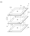
- FIG. FIG. 11 is an external perspective view of a multilayer ceramic capacitor 200 (third embodiment). 10 is a cross-sectional view taken along line XX of the multilayer ceramic capacitor 200 shown in FIG. 9. 2 is a schematic diagram showing the structure of an inner layer 6 of a multilayer ceramic capacitor 200.
- FIG. 11 is an external perspective view of a multilayer ceramic capacitor 200 (third embodiment).
- 10 is a cross-sectional view taken along line XX of the multilayer ceramic capacitor 200 shown in FIG. 9.
- FIG. 1 is a schematic perspective view of the multilayer ceramic capacitor 1.
- FIG. 2 is a cross-sectional view (LT cross-sectional view) of the multilayer ceramic capacitor 1 cut along line II-II at the center of the width direction W shown in FIG. 1.
- FIG. 3 is a cross-sectional view (WT cross-sectional view) of the multilayer ceramic capacitor 1 cut along line III-III at the center of the length direction L shown in FIG. 1.
- FIG. 4 is a schematic diagram showing the structure of an inner layer portion 6 of the multilayer ceramic capacitor 1.
- the stacking direction T the direction in which the dielectric layers 4 and the internal electrode layers 5 are stacked is defined as the stacking direction T, and the structure of the multilayer ceramic capacitor 1 will be described using the length direction L perpendicular to the stacking direction T and the width direction W perpendicular to the stacking direction T and the length direction L.
- the stacking direction T, the width direction W, and the length direction L are perpendicular to one another, but they are not necessarily perpendicular to one another and may intersect with one another.
- the multilayer ceramic capacitor 1 has a generally rectangular parallelepiped shape and comprises a laminate 2 and a pair of external electrodes 3 provided on both ends of the laminate 2.
- the laminate 2 includes an inner layer 6 that includes multiple pairs of dielectric layers 4 and internal electrode layers 5.
- a pair of outer surfaces facing each other in the stacking direction T are the first main surface A1 and the second main surface A2
- a pair of outer surfaces facing each other in the width direction W are the first side surface B1 and the second side surface B2
- a pair of outer surfaces facing each other in the length direction L are the first end surface C1 and the second end surface C2.
- first main surface A1 and the second main surface A2 when there is no need to distinguish between the first main surface A1 and the second main surface A2, they will be collectively referred to as the main surface A, when there is no need to distinguish between the first side surface B1 and the second side surface B2, they will be collectively referred to as the side surface B, and when there is no need to distinguish between the first end surface C1 and the second end surface C2, they will be collectively referred to as the end surface C.
- the dimensions of the multilayer ceramic capacitor 1 should not be particularly limited, but for example, the dimension in the stacking direction T can be 0.1 mm or more and 6.5 mm or less, the dimension in the length direction L can be 0.2 mm or more and 6.5 mm or less, and the dimension in the width direction W can be 0.1 mm or more and 5.5 mm or less.
- the laminate 2 includes an inner layer portion 6, an outer layer portion 7 disposed on the principal surface A side of the inner layer portion 6, and a side gap portion 8 disposed on the side surface B side of the inner layer portion 6.
- the laminate 2 preferably has a rounded ridge portion E.
- the ridge portion E is a portion where two surfaces of the laminate 2, i.e., the principal surface A and the side surface B, the principal surface A and the end surface C, or the side surface B and the end surface C, intersect, and also includes a corner portion where the principal surface A, the side surface B, and the end surface C intersect.
- the inner layer portion 6 is located between the internal electrode layer 5 closest to the first main surface A1 and the internal electrode layer 5 closest to the second main surface A2, and is a portion where multiple internal electrode layers 5 face each other via the dielectric layer 4 to form a capacitance.
- Figure 4 shows a schematic diagram of the structure of the inner layer 6.
- the dielectric layers 4 are integrated to the extent that the boundaries between the dielectric layers 4 are not visible.
- the internal electrode layer 5 is preferably, but not limited to, rectangular. The corners of the rectangle may be rounded or may be formed at an angle.
- the first internal electrode layer 5a is extended to a first end face C1 of the laminate 2, and the second internal electrode layer 5b is extended to a second end face C2 of the laminate 2.
- the internal electrode layer 5 is formed by sintering a conductive paste containing a metal powder that serves as a conductor, an organic solvent, a binder, and a dispersant on the dielectric layer 4.
- the internal electrode layer 5 and the dielectric layer 4 are alternately stacked to form the inner layer portion 6.
- the internal electrode layer 5 is composed of a first internal electrode layer 5a and a second internal electrode layer 5b, and the first internal electrode layer 5a and the second internal electrode layer 5b are disposed on the dielectric layers 4a and 4b, respectively. Note that when there is no need to distinguish between the first internal electrode layer 5a and the second internal electrode layer 5b, they will be collectively referred to as the internal electrode layer 5.
- the internal electrode layer 5 can be made of a conductive material such as, but not limited to, metals such as Ni, Cu, Ag, Pd, Au, or alloys containing at least one of these metals, such as Ag-Pd alloys.
- the thickness of the internal electrode layer 5 is not particularly limited, but can be, for example, about 0.3 ⁇ m to 1.5 ⁇ m.
- the internal electrode layer 5 includes an opposing electrode portion 52 where the first internal electrode layer 5a and the second internal electrode layer 5b face each other, and an extraction electrode portion 51 where the first internal electrode layer 5a and the second internal electrode layer 5b do not face each other and are drawn from the opposing electrode portion 52 to one end face C.
- the end of the extraction electrode portion 51 is exposed to the end face C and is electrically connected to the external electrode 3.
- the direction in which the extraction electrode portion 51 extends differs between the first internal electrode layer 5a and the second internal electrode layer 5b, and the extraction electrode portion 51 is drawn alternately to the first end face C1 side and the second end face C2 side.
- An electric charge is accumulated between the opposing electrode portions 52 of the first internal electrode layer 5a and the second internal electrode layer 5b adjacent to each other in the stacking direction T, and functions as a capacitor.
- each of the first internal electrode layer 5a and the second internal electrode layer 5b is preferably, for example, about 0.2 ⁇ m or more and 2.0 ⁇ m or less. In addition, it is preferable that the first internal electrode layer 5a and the second internal electrode layer 5b have a total of 2 layers or more and 2000 layers or less.
- the dielectric layer 4 can be formed of, for example, a ceramic material as a dielectric material.
- a ceramic material examples include BaTiO 3 , CaTiO 3 , SrTiO 3 , and CaZrO 3 .
- a secondary component such as, for example, a Si compound, a Mg compound, an Al compound, a Mn compound, a Sn compound, a Cu compound, a Ni compound, and a rare earth compound can be added depending on the desired characteristics of the laminate.
- the grain size of the crystals is 1 ⁇ m or less and the thickness of the dielectric layer is made thin.
- the dielectric layer 4 is composed of, for example, a sintered ceramic green sheet containing a ceramic material.
- the thickness of the dielectric layer 4 is not particularly limited, but can be, for example, about 0.2 ⁇ m to 10.0 ⁇ m in the effective capacitance formation area formed by the first internal electrode layer 5a and the second internal electrode layer 5b.
- the number of dielectric layers 4 is not particularly limited, but can be, for example, 2 to 2000 layers in the effective capacitance formation area formed by the first internal electrode layer 5a and the second internal electrode layer 5b.
- outer layer portions 7 On both the top and bottom of the inner layer portion 6, there are provided outer layer portions 7 which are composed only of dielectric layers and have no internal electrode layers 5.
- the thickness of the outer layer portions 7 is not limited, but may be, for example, 15 ⁇ m to 150 ⁇ m.
- the outer layer portions 7 are formed of a ceramic material and may be formed of the same material as the dielectric layer 4 of the inner layer portion 6.
- the thickness of the dielectric layer in the outer layer portion 7 may be greater than the thickness of the dielectric layer in the effective region of capacitance formation where the internal electrode layers 5 are formed.
- the material of the dielectric layer in the outer layer portion 7 may be different from the material of the dielectric layer 4 in the inner layer portion 6.
- the side gap portions 8 are provided on both side surfaces B of the inner layer portion 6 in the laminate 2.
- the dimension of the side gap portions 8 in the width direction W is preferably 5 ⁇ m or more and 40 ⁇ m or less, and particularly preferably 5 ⁇ m or more and 20 ⁇ m or less.
- the side gap portion 8 can be formed integrally with the inner layer portion 6 using the same material as the dielectric layer 4, but it may also be formed by attaching the same ceramic material as the dielectric layer 4 to both sides of the inner layer portion 6 in the width direction W.
- the side gap portion 8 is also called a W gap portion.
- Figure 5 shows an example in which ceramic material is applied to both sides of the inner layer 6 in the width direction W to form side gaps 81, 82.
- the side gaps 81, 82 can have a two-layer structure with inner layers 81a, 82a on the inside in the width direction W and outer layers 81b, 82b on the outside in the width direction.
- the side gap portion 8 is not limited to a two-layer structure consisting of the inner layers 81a, 82a and the outer layers 81b, 82b, but may be a structure of three or more layers.
- the multilayer ceramic capacitor 1 can reduce the mechanical and thermal stresses that it receives from the wiring board when mounted.
- providing the voids P allows moisture to penetrate into the inner layer portions 6 from the outside, which reduces the moisture resistance of the laminate 2, so it is necessary to adjust the porosity.
- the LT cross section at the center of the width direction W of the multilayer ceramic capacitor 1 is observed at 6000x magnification using a scanning electron microscope (SEM).
- SEM scanning electron microscope
- An area with a field of view size of 19.5 ⁇ m x 10.5 ⁇ m is photographed at five locations so that the areas do not overlap, and the ratio of the area occupied by voids P to the entire field of view is calculated as the porosity from each obtained SEM image by image analysis, and the average value for the five fields of view can be calculated.
- the voids P in the outermost layer 7bo located on the main surface A side contribute to stress relief and therefore have a relatively large void ratio S1
- the voids P in the innermost layer 7bi located on the inner layer portion 6 side contribute to moisture resistance and therefore have a relatively small void ratio S3.
- the porosity S1 of the outermost layer 7bo is preferably 10% or less
- the porosity S2 of the intermediate layer 7bm is preferably 5% or less
- the porosity S3 of the innermost layer 7bi is preferably 4% or less.
- the sinterability of the ceramic material is improved and the difference in shrinkage rate between the inner layer 6 and the outer layer 7 can be reduced. This makes it possible to prevent the outer layer 7 from peeling off from the inner layer 6.
- the adhesive strength between the inner layer 6 and the outer layer 7 can be increased. This makes it possible to reliably prevent the intrusion of moisture from the outside.
- the addition of Mg can suppress the grain growth of the ceramic grains, making it possible to form a dense layer structure.
- the composition of each component can be determined by cutting the multilayer ceramic capacitor to expose the dielectric ceramic layer and performing elemental analysis on the cut surface using wavelength dispersive X-ray analysis (WDX) or transmission electron microscope-energy dispersive X-ray analysis (TEM-EDX). At this time, the composition of each dielectric ceramic layer is measured at five points and the average value is calculated.
- WDX wavelength dispersive X-ray analysis
- TEM-EDX transmission electron microscope-energy dispersive X-ray analysis
- the content of Si segregated at the boundary between the outer layer 7 and the inner layer 6 is preferably higher than the content of Si in the intermediate layer 7m of the outer layer 7.
- the content of Mg segregated at the boundary between the outer layer 7 and the inner layer 6 is higher than the content of Mg in the intermediate layer 7m of the outer layer 7. This increases the density of the innermost layer 7bi, improving moisture resistance.
- the external electrodes 3 are electrically connected to the internal electrode layers 5 and function as external input/output terminals. On the surface of the laminate 2, a first external electrode 3a and a second external electrode 3b are formed.
- the first external electrode 3a is formed on the first end face C1 of the laminate 2.
- the first external electrode 3a is formed in a cap shape, with the edge portion extending from the first end face C1 of the laminate 2 to the first main face A1, the second main face A2, the first side face B1, and the second side face B2.
- the second external electrode 3b is formed on the second end face C2 of the laminate 2.
- the second external electrode 3b is formed in a cap shape, and the edge portion is formed extending from the second end face C2 of the laminate 2 to the first main face A1, the second main face A2, the first side face B1, and the second side face B2.
- the first internal electrode layer 5a extended to the first end face C1 of the laminate 2 is connected to the first external electrode 3a.
- the second internal electrode layer 5b extended to the second end face C2 of the laminate 2 is connected to the second external electrode 3b.
- the external electrode 3 can have a structure including, for example, a base electrode layer 30 and a plating layer 31 disposed on the base electrode layer 30.
- the base electrode layer 30 includes at least one layer selected from a baked layer, a conductive resin layer, a direct plating layer, etc., as described below.
- the baked layer is formed by applying a conductive paste containing glass and metal to the laminate 2 and baking it, and may be baked simultaneously with the internal electrode layer 5 or may be baked after baking the internal electrode layer 5.
- the baking temperature is preferably 700 to 900°C.
- the glass component contains at least one selected from B, Si, Ba, Mg, Al, Li, etc.
- the metal contains at least one selected from Cu, Ni, Ag, Pd, Ag-Pd alloy, Au, etc.
- the thickness of the baked layer is preferably, for example, 0.1 ⁇ m or more and 200 ⁇ m or less.
- the baked layer may also be multiple layers.
- the conductive resin layer is formed on the surface of the baked layer, or is formed directly on the surface of the laminate 2.
- the conductive resin layer may be a multi-layer structure.
- the conductive resin layer is formed by applying a conductive resin paste containing a thermosetting resin and a metal component onto the baking layer or onto the laminate 2, and then performing a heat treatment at a temperature of 250 to 550°C or higher to thermally cure the resin and form a conductive resin layer.
- the atmosphere during the heat treatment is preferably a N2 atmosphere.
- the thickness of the conductive resin layer at the center of the first end face C1 and the second end face C2 is preferably, for example, about 10 ⁇ m or more and 200 ⁇ m or less.
- the thickness of the conductive resin layer at the center in the length direction L on the first main face A1 and the second main face A2, the first side face B1 and the second side face B2 is preferably, for example, about 5 ⁇ m or more and 50 ⁇ m or less.
- thermosetting resins such as epoxy resin, phenol resin, urethane resin, silicone resin, polyimide resin, etc.
- epoxy resin which has excellent heat resistance, moisture resistance, adhesion, etc., is one of the most suitable resins.
- the amount of resin contained in the conductive resin layer is preferably 25 vol% or more and 65 vol% or less with respect to the volume of the entire conductive resin.
- the conductive resin layer preferably contains a curing agent in addition to the thermosetting resin.
- a curing agent in addition to the thermosetting resin.
- various known compounds such as phenol-based, amine-based, acid anhydride-based, and imidazole-based compounds can be used as the curing agent.
- the conductive resin layer contains a thermosetting resin, and is therefore more flexible than, for example, a conductive layer formed by firing a plating film or a conductive paste. For this reason, even if the ceramic electronic component is subjected to a physical shock or a shock caused by a thermal cycle, the conductive resin layer functions as a buffer layer and can prevent cracks in the ceramic electronic component.
- the metal powder contained in the conductive resin layer can be Ag, Cu, Ni, or an alloy of these.
- the Cu and Ni metal powders can be used with an Ag coating on the surface.
- the Cu metal powder can also be used with an anti-oxidation treatment on the surface.
- the reason for using Ag metal powder as the conductive metal is that Ag has the lowest resistivity of all metals, making it suitable as an electrode material, and because Ag is a precious metal, it does not oxidize and has high resistance.
- the reason for using Ag-coated metal is that it is possible to make the base metal cheaper while still maintaining the above-mentioned properties of Ag.
- the metal powder contained in the conductive resin layer is preferably contained in an amount of 35 vol% or more and 75 vol% or less relative to the total volume of the conductive resin.
- the shape of the metal powder contained in the conductive resin layer is not particularly limited.
- the metal powder may be spherical, flat, etc.
- the average particle size of the metal powder contained in the conductive resin layer is not particularly limited, but can be, for example, about 0.3 ⁇ m or more and 10 ⁇ m or less.
- the metal powder contained in the conductive resin layer is mainly responsible for the electrical conductivity of the conductive resin layer. Specifically, when the metal powder particles come into contact with each other, an electrical path is formed inside the conductive resin layer.
- a plating layer may be provided directly on the end surface C where the internal electrode layer 5 of the laminate 2 is exposed. That is, the multilayer ceramic capacitor 1 may have a structure including a plating layer that is electrically connected directly to the internal electrode layer 5 and the surface electrode 32. In such a case, a catalyst may be provided on the surface of the laminate 2 as a pretreatment, and then the plating layer may be formed directly.
- the plating layer preferably contains at least one metal selected from, for example, Cu, Ni, Sn, Pb, Au, Ag, Pd, Bi, or Zn, or an alloy containing these metals.
- the direct plating layer is formed using Cu, which has good bonding properties with Ni.
- each plating layer is preferably 1.0 ⁇ m or more and 15 ⁇ m or less.
- the plating layer preferably does not contain glass.
- the proportion of metal contained per unit volume of the plating layer is preferably 99 volume % or more.
- electrolytic plating When performing plating, either electrolytic plating or electroless plating may be used, but electroless plating has the disadvantage that pretreatment with a catalyst or the like is required to improve the plating deposition speed, which complicates the process. Therefore, it is usually preferable to use electrolytic plating.
- a plating method it is preferable to use barrel plating.
- an upper layer plating electrode may be formed on the surface of the lower layer plating electrode in the same manner.
- the plating layer 31 disposed on the base electrode layer 30 contains, for example, at least one selected from Cu, Ni, Ag, Pd, Ag-Pd alloy, Au, etc.
- the plating layer can be formed of multiple layers, for example, a two-layer structure of Ni plating and Sn plating is preferable.
- the Ni plating layer can prevent the underlying electrode layer from being eroded by solder when mounting ceramic electronic components, and the Sn plating layer improves the wettability of the solder when mounting ceramic electronic components, allowing for easy mounting.
- the thickness of each plating layer is preferably 1.0 ⁇ m or more and 15 ⁇ m or less.
- a surface electrode 32 can be provided on the main surface A of the laminate 2 with a predetermined length from an end surface C of the laminate 2 in the length direction L toward the center of the laminate 2.
- the surface electrode 32 can be formed integrally with the external electrode 3 by extending onto the main surface A, but as shown in Fig. 2, the surface electrode 32 can be formed on the main surface A of the laminate 2 in advance, and the surface electrode 32 can be covered by the portion of the external electrode 3 that extends onto the main surface A.
- FIG. 2 shows a configuration in which the surface electrode 32 is completely covered by the external electrode 3, but it may also be a configuration in which at least a portion of the surface electrode 32 is covered by a portion that extends onto the main surface A of the external electrode 3.
- a ceramic slurry for the inner layer is prepared by adding a solvent to a ceramic material for forming the dielectric layer for the inner layer. Then, the ceramic slurry for the inner layer is molded into a sheet to prepare a ceramic green sheet for the inner layer for lamination. A pattern of an internal electrode layer is printed on the surface of the ceramic green sheet for the inner layer for lamination with a conductive paste. Next, the ceramic green sheets for the inner layer for lamination are stacked and subjected to a hydrostatic press to prepare an inner layer block.
- a ceramic slurry for outer layers is prepared by adding a solvent or the like to a ceramic material for forming the outer dielectric layers, and the ceramic slurry for outer layers is molded into a sheet shape to prepare a ceramic green sheet for lamination.
- the laminated outer layer ceramic green sheets are stacked and subjected to isostatic pressing to prepare a first outer layer block and a second outer layer block. Since the first and second outer layer blocks are pressed together, the density is improved compared to normal integral pressing. Furthermore, the area at the beginning of lamination is more dense because more pressure is applied, while the area at the end of lamination is less dense than the area at the beginning of lamination.
- the denser parts of each laminate sheet are brought to the inner layer side, making it possible to make the inner layer side region into a denser region.
- the surface electrode by forming the surface electrode before isostatically pressing the first outer layer block and the second outer layer block, it is no longer necessary to remove one dielectric sheet to expose the conventional surface electrode, and the surface shape of the surface electrode can be made similar on the first main surface side and the second main surface side.
- first outer layer block, the inner layer block, and the second outer layer block are stacked together and pressed at a pressure of 1-50 MPa, a press temperature of 70-90°C, and a hold time of 180 seconds or less at maximum press pressure. This completes the mother block member.
- the mother block member is divided along cutting lines that correspond to the dimensions of the laminate to produce multiple laminated chips.
- the laminated chips are then barrel polished to round off the corners and edges, and then fired.
- the outer layer portion 7 and the side gap portion 8 can be formed at the same time as the laminate 2 is formed.
- the inner layer portion 6 can be first formed with the ends of the internal electrode layers 5 in the width direction W exposed on both sides, and then the laminate 2 can be formed by attaching a ceramic material to both sides of the inner layer portion 6 so as to cover the exposed ends of the internal electrode layers 5.
- the laminate 2 formed in this way can have side gap portions 81, 82 as shown in FIG. 5.
- the firing process In the firing process, the laminated chip is subjected to a binder removal process and a firing process to form an element part.
- the conductive paste layer and the green sheet for the dielectric layer are co-sintered by the firing process to form the internal electrode layer 5 and the dielectric layer 4, respectively.
- the conditions for the binder removal process may be determined according to the type of organic binder contained in the green sheet and the conductive paste layer.
- the firing process may be performed at a temperature at which the laminated chip is sufficiently densified. The firing temperature depends on the materials of the dielectric and the internal electrode layer, but is preferably 900°C to 1400°C.
- the external electrodes 3 are formed on the laminate 2 to form the multilayer ceramic capacitor 1.
- the external electrodes 3 may be formed by a known method. For example, On the exposed end surface C, a base electrode layer, a conductive resin layer or a direct plating layer is formed, and further, a plating layer is provided as necessary. In this embodiment, a Ni plating layer and a Sn plating layer are formed on the baked layer. The Ni plating layer and the Sn plating layer are successively formed by, for example, barrel plating, and thus a multilayer ceramic capacitor can be obtained.
- FIG. 1 A multilayer ceramic capacitor 100 will be described as the second embodiment.
- Figures 6 to 8 show the shape and structure of the multilayer ceramic capacitor 100.
- Figure 6 is a schematic perspective view of the multilayer ceramic capacitor 100.
- Figure 7 is a cross-sectional view of the multilayer ceramic capacitor 100 taken along line VII-VII shown in Figure 6.
- Figure 8 is a schematic view showing the structure of an inner layer 6 of the multilayer ceramic capacitor 100.
- the multilayer ceramic capacitor 100 will be described focusing on the configuration that differs from the multilayer ceramic capacitor 1 of the first embodiment.
- the multilayer ceramic capacitor 100 of this embodiment includes a laminate 2 and four external electrodes 3 .
- the external electrodes 3 are disposed at each of the four corners when the laminate 2 is viewed along the stacking direction T.
- the external electrodes 3 are disposed so as to cover a part of the first main surface A1, a part of the second main surface A2, a part of either the first side surface B1 or the second side surface B2, and a part of either the first end surface C1 or the second end surface C2 of the laminate 2, but are not limited to this, and the external electrodes may be disposed so as not to cover a part of the first main surface A1 or the second main surface A2 in order to further reduce the dimension in the stacking direction T.
- the external electrodes are substantially L-shaped.
- the ratio Y/X of the length Y in the width direction W to the length X in the length direction L of the multilayer ceramic capacitor 100 in this embodiment is 0.85 or more and 1.0 or less, but is not limited to this.
- the ratio Y/X of the length Y to the length X is less than 0.85, the shape will be closer to a substantially rectangular shape rather than a substantially square shape.
- the height of the multilayer ceramic capacitor 100 i.e., the dimension in the stacking direction T, is 120 ⁇ m or less.
- the first internal electrode layer 5a of this embodiment has an opposing electrode portion 52 and two lead-out electrode portions 51.
- Each lead-out electrode portion 51 is exposed to either the first side surface B1 or the second side surface B2 and either the first end surface C1 or the second end surface C2.
- the lead-out electrode portions 51 of the two first internal electrode layers 5a facing each other in the stacking direction T are led out to two different surfaces.
- the other first internal electrode layer 5a has a lead-out electrode portion 51 led out to the first side surface B1 and the first end surface C1, and a lead-out electrode portion 51 led out to the second side surface B2 and the second end surface C2
- the other first internal electrode layer 5a has a lead-out electrode portion 51 led out to the first side surface B1 and the second end surface C2
- the lead electrode portion 51 is continuously exposed from the end face to the side face, but this is not limited thereto, and it may be discontinuously exposed from the end face to the side face.
- a dielectric layer 114a is formed around the opposing electrode portion 52 of the first internal electrode layer 5a, except for the portion from which the lead electrode portion 51 extends.
- the second internal electrode layer 5b is disposed at a position shifted from the lead electrode portion 51 of the first internal electrode layer 5a in the stacking direction T. In other words, the second internal electrode layer 5b is disposed at a position overlapping the lead electrode portion 51 of the first internal electrode layer 5a when viewed along the stacking direction T.
- the two second internal electrode layers 5b may also be disposed on the same plane.
- the two second internal electrode layers 5b disposed on the same plane are disposed without overlapping each other when viewed along the stacking direction T, and a dielectric layer 114b is disposed between the two second internal electrode layers 5b.
- the second internal electrode layer 5b By disposing the second internal electrode layer 5b on each of the two outer layer portions 7a, 7b, it is possible to ensure electrical connectivity between the first surface electrode 132a and the second surface electrode 132b described later and the first internal electrode layer 5a via the base electrode layer 30. In addition, the adhesion between the second internal electrode layer 5b and the conductive component in the external electrode 3 can improve the adhesion between the laminate 2 and the external electrode 3.
- first surface electrodes 132a are arranged on the first main surface A1 of the laminate 2.
- second surface electrodes 132b are arranged on the second main surface A2 of the laminate 2.
- the first surface electrodes 132a are arranged at each of the four corners of the first main surface A1.
- the second surface electrodes 132b are arranged at each of the four corners of the second main surface A2.
- the first surface electrodes 132a and the second surface electrodes 132b are arranged at positions shifted in the stacking direction T from the lead electrode portion 51 of the first internal electrode layer 5a.
- first surface electrodes 132a and the second surface electrodes 132b are arranged at positions overlapping with the lead electrode portion 51 of the first internal electrode layer 5a when viewed along the stacking direction T.
- the first surface electrode 132a and the second surface electrode 132b are electrodes that do not form a capacitance.
- the first surface electrode 132a and the second surface electrode 132b may have the same shape and dimensions as the second internal electrode layer 5b. In this case, it is preferable that the first surface electrode 132a and the second surface electrode 132b are made of the same material as the second internal electrode layer 5b.
- the first surface electrode 132a and the second surface electrode 132b may be formed by a sputtering method.
- the first surface electrode 132a and the second surface electrode 132b preferably contain at least one selected from Ni, Cr, Cu, and Ti.
- the thickness of the first surface electrode 132a and the second surface electrode 132b formed by the sputtering method is preferably 50 nm or more and 400 nm or less. This allows the thickness of the first surface electrode 132a and the second surface electrode 132b in the stacking direction T to be sufficiently thin, and therefore the thickness of the multilayer ceramic capacitor 100 in the stacking direction T to be sufficiently thin.
- the thickness of the first surface electrode 132a and the second surface electrode 132b in the stacking direction T can be adjusted by changing the distance between the part to be sputtered and the target.
- the thickness of the first surface electrode 132a and the second surface electrode 132b may be measured from an actual observation image, or may be measured by converting the thickness from a specified element using a calibration curve method for metal species using fluorescent X-rays.
- the first surface electrode 132a and the second surface electrode 132b may be sintered electrodes.
- a sintered electrode is an electrode containing the same type of dielectric component as the dielectric layer 4. That is, when the dielectric layer 4 contains CaZrO3 , the first surface electrode 132a and the second surface electrode 132b contain, for example, Ca or Zr, CaZrO3 . When the dielectric layer 4a and the dielectric layer 4b have different components, it is preferable that the first surface electrode 132a and the second surface electrode 132b contain the same type of component as the dielectric layer 4b. This can further strengthen the adhesion between the dielectric layer 4b and the first surface electrode 132a and the second surface electrode 132b.
- the metal components in the fired electrodes preferably contain Ni.
- the first internal electrode layer 5a preferably contains Ni.
- the fired electrodes are formed by printing the conductive paste for Ni fired electrodes onto a dielectric sheet using screen printing or the like, followed by firing. At this time, by applying a thin layer of the conductive paste for Ni fired electrodes, or by reducing the dielectric components contained in the conductive paste for Ni fired electrodes, the Ni particles bond together during firing, forming a discontinuous fired electrode.
- a discontinuous fired electrode means that the fired electrodes are arranged discontinuously when viewed along the width direction W.
- the external electrode 3 has a base electrode layer 30 containing a conductive metal arranged on the laminate 2, a base plating layer 31a arranged to cover the surface of the base electrode layer 30, and a top plating layer 31b arranged to cover the surface of the base plating layer 31a.
- the base plating layer 31a is a Ni plating layer
- the top plating layer 31b is a Sn plating layer.
- the base electrode layer 30, base plating layer 31a, and top plating layer 31b are arranged in this order, but they may also be arranged in the order of base electrode layer, top plating layer, base plating layer, and top plating layer.
- the base electrode layer 30 is preferably formed by a direct plating layer.
- a direct plating layer is a plating layer that directly covers the surface of the laminate 2. By using a direct plating layer as the base electrode layer 30, the thickness of the external electrode 3 can be reduced in each direction, allowing the laminate ceramic capacitor to be made smaller.
- the metal ratio per unit volume of the direct plating layer is preferably 99 volume percent or more.
- the direct plating may have two plating layers with different metal particle sizes. In this case, it is preferable that the plating layer with the larger metal particle size is arranged on the side closer to the laminate 2, and the plating layer with the smaller metal particle size is arranged on the side farther from the laminate 2.
- the multilayer ceramic capacitor 100 of the second embodiment can achieve the same effects as the multilayer ceramic capacitor 1 of the first embodiment.
- a multilayer ceramic capacitor 200 will be described as the third embodiment.
- the multilayer ceramic capacitor 200 will be described focusing on the configuration different from the multilayer ceramic capacitor 1 of the first embodiment and the multilayer ceramic capacitor 100 of the second embodiment.
- the multilayer ceramic capacitor 200 according to the third embodiment has a similar configuration to the multilayer ceramic capacitor 100 according to the second embodiment, except for its overall shape.
- configurations that are the same as or similar to those in the second embodiment are indicated with the same or similar reference symbols, and detailed descriptions thereof are omitted.
- FIG. 9 is a perspective view of a multilayer ceramic capacitor 200 according to this embodiment.
- FIG. 10 is a cross-sectional view taken along line X-X in FIG. 9.
- FIG. 11 is an exploded perspective view of an inner layer portion 6 according to this embodiment.
- the length of the multilayer ceramic capacitor 200 in the length direction L is shorter than the length in the width direction W.
- each first internal electrode layer 5a is exposed to either the first end face C1 or the second end face C2, but this is not limited thereto, and each first internal electrode layer 5a may be exposed to either the first end face C1 or the second end face C2, the first side face B1, and the second side face B2.
- the above describes an embodiment of the present invention, but the present invention is not limited to the embodiment, and can be implemented in various forms without departing from the gist of the present invention.
- the present invention includes the following combinations.
- a laminate including an inner layer portion in which dielectric layers and internal electrode layers are alternately laminated, and two outer layer portions that are arranged to sandwich the inner layer portion from the lamination direction and form two main surfaces at positions opposite to each other in the lamination direction; external electrodes disposed on both end faces of the laminate in a longitudinal direction intersecting the lamination direction and connected to the internal electrode layers;
- a multilayer ceramic capacitor having A multilayer ceramic capacitor, in which, when one of the two outer layer portions sandwiching the inner layer portion is divided into three equal parts in the stacking direction, a porosity S1 of the outermost layer located on the main surface side, a porosity S2 of an intermediate layer, and a porosity S3 of the innermost layer located on the inner layer portion side satisfy the following relational expression (1): S1>S2>S3...(1)
- ⁇ 3> A multilayer ceramic capacitor according to ⁇ 1> or ⁇ 2>, in which the porosity S1 of the outermost layer is 1% or more and 10% or less.
- ⁇ 4> A multilayer ceramic capacitor according to any one of ⁇ 1> to ⁇ 3>, in which the porosity S2 of the intermediate layer is 1% or more and 5% or less.
- ⁇ 5> A multilayer ceramic capacitor according to any one of ⁇ 1> to ⁇ 4>, in which the porosity S3 of the innermost layer is 1% or more and 4% or less.
- ⁇ 6> A multilayer ceramic capacitor according to any one of ⁇ 1> to ⁇ 5>, in which the Si content at the boundary between the outer layer and the inner layer is higher than the Si content in the intermediate layer of the outer layer.
- ⁇ 7> A multilayer ceramic capacitor according to any one of ⁇ 1> to ⁇ 6>, in which the Mg content at the boundary between the outer layer and the inner layer is higher than the Mg content in the intermediate layer of the outer layer.
- a multilayer ceramic capacitor according to ⁇ 8> in which at least a portion of the surface electrode is covered by a portion of the external electrode that extends onto the main surface.
Landscapes
- Engineering & Computer Science (AREA)
- Power Engineering (AREA)
- Manufacturing & Machinery (AREA)
- Microelectronics & Electronic Packaging (AREA)
- Chemical & Material Sciences (AREA)
- Ceramic Engineering (AREA)
- Inorganic Chemistry (AREA)
- Ceramic Capacitors (AREA)
- Fixed Capacitors And Capacitor Manufacturing Machines (AREA)
Priority Applications (3)
| Application Number | Priority Date | Filing Date | Title |
|---|---|---|---|
| CN202480009807.3A CN120548581A (zh) | 2023-02-01 | 2024-01-15 | 层叠陶瓷电容器 |
| JP2024574391A JPWO2024161970A1 (enExample) | 2023-02-01 | 2024-01-15 | |
| US19/281,798 US20250357048A1 (en) | 2023-02-01 | 2025-07-28 | Multilayer ceramic capacitor |
Applications Claiming Priority (2)
| Application Number | Priority Date | Filing Date | Title |
|---|---|---|---|
| JP2023-014099 | 2023-02-01 | ||
| JP2023014099 | 2023-02-01 |
Related Child Applications (1)
| Application Number | Title | Priority Date | Filing Date |
|---|---|---|---|
| US19/281,798 Continuation US20250357048A1 (en) | 2023-02-01 | 2025-07-28 | Multilayer ceramic capacitor |
Publications (1)
| Publication Number | Publication Date |
|---|---|
| WO2024161970A1 true WO2024161970A1 (ja) | 2024-08-08 |
Family
ID=92146314
Family Applications (1)
| Application Number | Title | Priority Date | Filing Date |
|---|---|---|---|
| PCT/JP2024/000838 Ceased WO2024161970A1 (ja) | 2023-02-01 | 2024-01-15 | 積層セラミックコンデンサ |
Country Status (4)
| Country | Link |
|---|---|
| US (1) | US20250357048A1 (enExample) |
| JP (1) | JPWO2024161970A1 (enExample) |
| CN (1) | CN120548581A (enExample) |
| WO (1) | WO2024161970A1 (enExample) |
Cited By (1)
| Publication number | Priority date | Publication date | Assignee | Title |
|---|---|---|---|---|
| US20250292966A1 (en) * | 2024-03-13 | 2025-09-18 | Murata Manufacturing Co., Ltd. | Multilayer ceramic capacitor |
Citations (3)
| Publication number | Priority date | Publication date | Assignee | Title |
|---|---|---|---|---|
| JP2020025146A (ja) * | 2014-05-21 | 2020-02-13 | 株式会社村田製作所 | 積層セラミックコンデンサ |
| JP2020141091A (ja) * | 2019-03-01 | 2020-09-03 | 太陽誘電株式会社 | 積層セラミックコンデンサ及びその製造方法 |
| JP2022099274A (ja) * | 2020-12-22 | 2022-07-04 | サムソン エレクトロ-メカニックス カンパニーリミテッド. | 積層型キャパシタ及びその実装基板 |
-
2024
- 2024-01-15 CN CN202480009807.3A patent/CN120548581A/zh active Pending
- 2024-01-15 WO PCT/JP2024/000838 patent/WO2024161970A1/ja not_active Ceased
- 2024-01-15 JP JP2024574391A patent/JPWO2024161970A1/ja active Pending
-
2025
- 2025-07-28 US US19/281,798 patent/US20250357048A1/en active Pending
Patent Citations (3)
| Publication number | Priority date | Publication date | Assignee | Title |
|---|---|---|---|---|
| JP2020025146A (ja) * | 2014-05-21 | 2020-02-13 | 株式会社村田製作所 | 積層セラミックコンデンサ |
| JP2020141091A (ja) * | 2019-03-01 | 2020-09-03 | 太陽誘電株式会社 | 積層セラミックコンデンサ及びその製造方法 |
| JP2022099274A (ja) * | 2020-12-22 | 2022-07-04 | サムソン エレクトロ-メカニックス カンパニーリミテッド. | 積層型キャパシタ及びその実装基板 |
Cited By (1)
| Publication number | Priority date | Publication date | Assignee | Title |
|---|---|---|---|---|
| US20250292966A1 (en) * | 2024-03-13 | 2025-09-18 | Murata Manufacturing Co., Ltd. | Multilayer ceramic capacitor |
Also Published As
| Publication number | Publication date |
|---|---|
| US20250357048A1 (en) | 2025-11-20 |
| JPWO2024161970A1 (enExample) | 2024-08-08 |
| CN120548581A (zh) | 2025-08-26 |
Similar Documents
| Publication | Publication Date | Title |
|---|---|---|
| US11239030B2 (en) | Electronic component | |
| KR101823246B1 (ko) | 적층 세라믹 전자 부품 및 그 실장 기판 | |
| KR101788097B1 (ko) | 적층 세라믹 콘덴서, 이것을 포함하는 적층 세라믹 콘덴서 시리즈, 및 적층 세라믹 콘덴서의 실장체 | |
| CN105097282B (zh) | 层叠陶瓷电容器 | |
| JP7081543B2 (ja) | 積層セラミックコンデンサ | |
| US9232673B2 (en) | Ceramic electronic component including coating layer | |
| JP7363654B2 (ja) | 積層セラミック電子部品 | |
| KR101927731B1 (ko) | 적층 세라믹 콘덴서 | |
| JP2020035788A (ja) | 電子部品 | |
| JP7670193B2 (ja) | 積層セラミックコンデンサおよび積層セラミックコンデンサの実装構造 | |
| US11094462B2 (en) | Multilayer ceramic electronic component | |
| JP2020077815A (ja) | 積層セラミックコンデンサ | |
| US11721482B2 (en) | Method of producing ceramic electronic component and ceramic electronic component | |
| KR101434103B1 (ko) | 적층 세라믹 전자부품 및 적층 세라믹 전자부품의 실장 기판 | |
| JP2023013421A (ja) | 積層セラミック電子部品 | |
| JP2020068375A (ja) | 積層セラミック電子部品 | |
| WO2024161743A1 (ja) | 積層セラミックコンデンサ | |
| US20250357048A1 (en) | Multilayer ceramic capacitor | |
| US20240395467A1 (en) | Multilayer ceramic capacitor | |
| JP7180569B2 (ja) | 積層セラミック電子部品 | |
| KR20150012075A (ko) | 적층 세라믹 전자부품 및 적층 세라믹 전자부품의 실장 기판 | |
| KR20260040334A (ko) | 적층 세라믹 콘덴서 | |
| WO2024018718A1 (ja) | 積層セラミック電子部品および積層セラミック電子部品の実装構造 | |
| WO2025047205A1 (ja) | 積層セラミックコンデンサ | |
| CN121753127A (zh) | 层叠陶瓷电容器 |
Legal Events
| Date | Code | Title | Description |
|---|---|---|---|
| 121 | Ep: the epo has been informed by wipo that ep was designated in this application |
Ref document number: 24749924 Country of ref document: EP Kind code of ref document: A1 |
|
| ENP | Entry into the national phase |
Ref document number: 2024574391 Country of ref document: JP Kind code of ref document: A |
|
| WWE | Wipo information: entry into national phase |
Ref document number: 2024574391 Country of ref document: JP |
|
| WWE | Wipo information: entry into national phase |
Ref document number: 202480009807.3 Country of ref document: CN |
|
| WWP | Wipo information: published in national office |
Ref document number: 202480009807.3 Country of ref document: CN |
|
| NENP | Non-entry into the national phase |
Ref country code: DE |
|
| 122 | Ep: pct application non-entry in european phase |
Ref document number: 24749924 Country of ref document: EP Kind code of ref document: A1 |