WO2024154790A1 - 配線基板、電気装置および電気装置構造体 - Google Patents
配線基板、電気装置および電気装置構造体 Download PDFInfo
- Publication number
- WO2024154790A1 WO2024154790A1 PCT/JP2024/001321 JP2024001321W WO2024154790A1 WO 2024154790 A1 WO2024154790 A1 WO 2024154790A1 JP 2024001321 W JP2024001321 W JP 2024001321W WO 2024154790 A1 WO2024154790 A1 WO 2024154790A1
- Authority
- WO
- WIPO (PCT)
- Prior art keywords
- organic resin
- wiring layer
- base
- conductor
- resin base
- Prior art date
- Legal status (The legal status is an assumption and is not a legal conclusion. Google has not performed a legal analysis and makes no representation as to the accuracy of the status listed.)
- Ceased
Links
Images


Classifications
-
- H—ELECTRICITY
- H05—ELECTRIC TECHNIQUES NOT OTHERWISE PROVIDED FOR
- H05K—PRINTED CIRCUITS; CASINGS OR CONSTRUCTIONAL DETAILS OF ELECTRIC APPARATUS; MANUFACTURE OF ASSEMBLAGES OF ELECTRICAL COMPONENTS
- H05K1/00—Printed circuits
- H05K1/02—Details
-
- H—ELECTRICITY
- H05—ELECTRIC TECHNIQUES NOT OTHERWISE PROVIDED FOR
- H05K—PRINTED CIRCUITS; CASINGS OR CONSTRUCTIONAL DETAILS OF ELECTRIC APPARATUS; MANUFACTURE OF ASSEMBLAGES OF ELECTRICAL COMPONENTS
- H05K3/00—Apparatus or processes for manufacturing printed circuits
- H05K3/46—Manufacturing multilayer circuits
Definitions
- the disclosed embodiments relate to wiring boards, electrical devices, and electrical device structures.
- a wiring board has been proposed in which multiple circuit sections made of organic resin are laminated on a ceramic substrate.
- the circuit sections are provided with multiple connection conductors that penetrate between the laminated layers.
- the wiring board according to one aspect of the embodiment has a base and a conductor.
- the base is a laminate of a ceramic base wiring layer and an organic resin base wiring layer.
- the organic resin base wiring layer has an organic resin base as an insulating base.
- the ceramic base wiring layer has a ceramic base as an insulating base.
- the organic resin base has a higher thermal expansion coefficient than the ceramic base.
- FIG. 1 is an explanatory diagram illustrating an example of an electric device structure according to an embodiment.
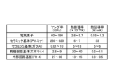
- FIG. 2 is a diagram showing an example of the characteristics of each member constituting an electric device structure.
- FIG. 3 is a cross-sectional view showing an example of the wiring board according to the first embodiment.
- FIG. 4 is a cross-sectional view showing an example of a wiring board according to the second embodiment.
- FIG. 5 is a cross-sectional view showing an example of a wiring board according to the third embodiment.
- FIG. 6 is an enlarged plan view of a portion of the wiring board shown in FIG.
- FIG. 7 is a cross-sectional view showing an example of a wiring board according to the fourth embodiment.
- FIG. 8 is a cross-sectional view showing an example of a wiring board according to the fifth embodiment.
- FIG. 9 is a cross-sectional view showing another example of the wiring board according to the embodiment.
- FIG. 10 is a cross-sectional view showing another example of the wiring board according to the embodiment.
- FIG. 11 is an explanatory diagram showing an example of a method for manufacturing a wiring board according to sample 1.
- FIG. 12 is a plan view showing a wiring board according to an experimental example.
- FIG. 13 is a diagram showing the evaluation results of the wiring board according to the experimental example.
- the ceramic layer is disposed on the external circuit board side, so there is room for improvement in that the reliability of the connection between the ceramic layer and the external circuit board is easily reduced due to the difference in the thermal expansion coefficient between the ceramic layer and the external circuit board.
- the electric device structure 5 has an electric device 3 and an external circuit board 4.
- the electric device 3 has a wiring board 1 and an electric element 2.
- the electric element 2 is mounted on a first surface 101 side of the wiring board 1, and the external circuit board 4 is connected to a second surface 201 side of the wiring board 1.
- the wiring board 1 has a ceramic base wiring layer (see Figure 3) located on the first surface 101 side, and an organic resin base wiring layer (see Figure 3) located on the second surface 201 side.
- the electrical device structure 5 has a structure in which an electrical element 2, a ceramic base wiring layer, an organic resin base wiring layer, and an external circuit board 4 are layered in this order.
- the ceramic base wiring layer has a ceramic base as an insulating base.
- the organic resin base wiring layer has an organic resin base as an insulating base.
- the order of the thermal expansion coefficients of the components that make up the electrical device structure 5 is, for example, electrical element ⁇ ceramic substrate wiring layer ⁇ organic resin substrate wiring layer.
- the external circuit board 4 has, for example, a thermal expansion coefficient equivalent to that of the organic resin substrate wiring layer.
- Figure 2 shows an example of the characteristics of each member that constitutes an electrical device structure.
- the order of thermal expansion coefficient is, for example, electrical element ⁇ ceramic substrate ⁇ organic resin substrate.
- the Young's modulus of the ceramic substrate is higher than that of the organic resin substrate. Since the ceramic substrate has a higher Young's modulus and a smaller thermal expansion coefficient than the organic resin substrate, mounting the electrical element 2 on the ceramic substrate wiring layer side of the wiring board 1 provides higher durability against thermal stress.
- the electric element 2 generates heat when it is driven. If the electric element 2 is mounted on a ceramic substrate wiring layer with high thermal conductivity, the heat dissipation from the ceramic substrate wiring layer to the outside is improved.
- the external circuit board 4 is generally larger in size than the wiring board 1, so even if the external circuit board 4 and the organic resin base wiring layer of the wiring board 1 have the same thermal expansion coefficient, the amount of deformation (elongation) will be greater in the external circuit board 4. However, if an organic resin base wiring layer is disposed between the ceramic base wiring layer and the external circuit board 4, the transfer of heat from the electrical element 2 to the external circuit board 4 can be reduced. As a result, the amount of deformation of the external circuit board 4 can be reduced, thereby improving the connection reliability of the connection points between the various components of the electrical device structure 5.
- the electrical element 2 would be directly mounted on the surface of the organic resin base wiring layer.
- there is a large difference in the thermal expansion coefficient between the electrical element 2 and the organic resin base wiring layer so there is a high possibility that a malfunction will occur in the electrical element 2 due to the thermal expansion of the organic resin base wiring layer.
- electrical device structures 5 having electrical elements 2 that are large (20 mm square or more) such malfunctions are likely to be noticeable.
- the ceramic substrate wiring layer will be directly connected to the external circuit board 4.
- the difference in thermal expansion coefficient between the ceramic substrate wiring layer and the external circuit board 4 is large, and therefore the reliability of the mounting on the external circuit board 4 (called secondary mounting; the electrical element 2 side is considered to be primary mounting) is likely to be compromised.
- the external circuit board 4 may be, for example, a composite of organic resin and glass cloth.
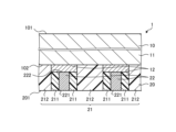
- FIG. 3 is a cross-sectional view showing an example of a wiring board according to the first embodiment.
- the wiring board 1 has a base and a conductor.
- the base is a laminate of a ceramic base wiring layer 10 and an organic resin base wiring layer 20.
- the organic resin base wiring layer 20 has an organic resin base 21 as an insulating base.
- the ceramic base wiring layer 10 has a ceramic base 11 as an insulating base.
- the organic resin base 21 has a higher thermal expansion coefficient than the ceramic base 11.
- the first terminal group (not shown) is provided on the first surface 101 of the laminate.
- the second terminal group (not shown) is provided on the second surface 201 of the laminate.
- the first surface 101 is a surface on which an electric element 2 (see FIG. 1) is mounted, and the second surface 201 is a surface for connection with an external circuit board 4 (see FIG. 1).
- the wiring board 1 has a ceramic base wiring layer 10 and an organic resin base wiring layer 20.
- the wiring board 1 has a first surface 101 located on the surface facing the ceramic base wiring layer 10, and a second surface 201 located on the surface facing the organic resin base wiring layer 20.
- the ceramic substrate wiring layer 10 has a ceramic substrate 11 and a surface conductor layer 12.
- the ceramic substrate 11 is, for example, an insulating substrate made of ceramics.
- the ceramic substrate 11 may be, for example, an alumina-based or glass ceramic-based ceramic, or may be a dielectric material such as cordierite, zirconia, barium titanate, strontium titanate, calcium titanate, aluminum titanate, lead zirconate titanate (PZT), etc.
- the ceramic substrate 11 may also have, for example, multiple ceramics.
- the surface conductor layer 12 is located on the surface of the ceramic base 11.
- the surface conductor layer 12 protrudes from the third surface 102.
- the third surface 102 is the surface of the ceramic base wiring layer 10 that contacts the organic resin base wiring layer 20.
- the surface conductor layer 12 may be, for example, a line-shaped wiring, a pad having a circular, rectangular or other angular shape, or a solid-shaped power supply layer or ground layer.
- the surface conductor layer 12 may be, for example, smaller than the area of the main surface of the ceramic base wiring layer 10.
- FIG. 3 an example is shown in which the surface conductor layer 12 protrudes from the third surface 102 of the ceramic substrate wiring layer 10 by a thickness equivalent to the thickness of the surface conductor layer 12.
- the surface conductor layer 12 may protrude from the third surface 102 of the ceramic substrate wiring layer 10 by a smaller proportion than the thickness of the surface conductor layer 12.
- the surface conductor layer 12 may be, for example, a conductor such as tungsten (W), molybdenum (Mo), a W-Mo mixture, a W-Mo alloy, a W-Mo intermetallic compound, copper (Cu), silver (Ag), or nickel (Ni).
- the surface conductor layer 12 may also contain ceramic powder, etc.
- the organic resin base wiring layer 20 is located below the ceramic base wiring layer 10.
- the organic resin base wiring layer 20 has an organic resin base 21 and a plurality of interlayer connection conductors 22.
- the organic resin base 21 has, for example, an organic material as an insulating base.
- the organic resin base 21 may be, for example, an epoxy resin, an acrylic resin, a polycarbonate resin, a polyimide resin, an olefin resin, or a polyphenylene resin.
- the organic resin base 21 may also be, for example, polytetrafluoroethylene (PTFE) or other fluororesins or polyphenylene ether resins.
- PTFE polytetrafluoroethylene
- the interlayer connection conductor 22 extends in the thickness direction of the organic resin base wiring layer 20, and is positioned so that one end 221 is exposed on the second surface 201, which is the surface of the organic resin base wiring layer 20.
- the other end 222 of the interlayer connection conductor 22 is electrically connected to the surface conductor layer 12.
- the interlayer connection conductor 22 may contain, for example, copper powder, tin (Sn) powder, and bismuth (Bi) powder.
- the ratio of the metal components such as copper, tin, and bismuth described above is preferably 60% or more and 90% or less in volume ratio.
- the conductivity of the interlayer connection conductor 22 can be increased.
- the adhesion between the organic resin base 21 and the surface conductor layer 12 and the interlayer connection conductor 22 can be increased.
- the ratio of the metal components may be determined as an area ratio by, for example, using an electron microscope equipped with an analyzer to view the cross section of the interlayer connection conductor 22.
- the determined area ratio may be regarded as a volume ratio.
- the total amount of copper, tin, and bismuth is preferably the same.
- the amount of tin and bismuth is preferably the same.
- the interlayer connection conductor 22 may have the same material as the organic resin base 21, such as epoxy resin, as the remainder.
- the organic resin base 21 also has a first region 211 and a second region 212.
- the first region 211 is a portion of the organic resin base 21 that is located on the surface conductor layer 12.
- the second region 212 is a portion of the organic resin base 21 that is located on the other part of the organic resin base 21 than the first region 211.
- the wiring board 1 may have a higher density in the first region 211 of the organic resin base 21 located on the surface conductor layer 12 compared to the density of the second region 212 located outside the range of the surface conductor layer 12. For example, if the surface conductor layer 12 is provided on the third surface 102 of the ceramic base 11 and an interlayer connection conductor 22 is provided in the organic resin base wiring layer 20, moisture is less likely to penetrate from the second region 212 of the organic resin base 21 to the first region 211 around the interlayer connection conductor 22. This allows the wiring board 1 to reduce a decrease in insulation resistance.
- the methods for evaluating density include determining the number or total area ratio of voids found in the first region 211 and the second region 212, and cutting out the first region 211 and the second region 212 and measuring the density of that portion.
- the method of determining the total area ratio of voids present in an area per unit area is preferable, as differences are likely to appear even in very small areas.
- the ceramic substrate wiring layer 10 may have, for example, a conductor layer located inside the ceramic substrate 11.
- the ceramic substrate wiring layer 10 may have, for example, a plurality of ceramic substrates 11 stacked in the thickness direction.
- the organic resin base wiring layer 20 may also have, for example, a conductor layer located inside and/or on the surface of the organic resin base 21.
- Second Embodiment 4 is a cross-sectional view showing an example of a wiring board according to the second embodiment.
- the wiring board 1 may have a coated conductor layer 30 located on the surface conductor layer 12.
- the thickness of the first region 211 of the organic resin base 21 becomes even smaller than that of the second region 212.
- the first region 211 may also be even denser than the second region 212. This makes it even more difficult for moisture to penetrate from the first region 211 to the interlayer connection conductor 22, for example, and improves the electrical reliability of the interlayer connection conductor 22.
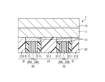
- Third Embodiment 5 is a cross-sectional view showing an example of a wiring board according to the third embodiment.
- FIG. 6 is an enlarged plan view of a part of the wiring board shown in FIG. 5.
- the interlayer connection conductor 22 constituting the organic resin base wiring layer 20 may have an inner region 22a and an outer periphery region 22b.
- the inner region 22a is located inside the outer periphery region 22b when the organic resin base wiring layer 20 is viewed in plan.
- the inner region 22a is surrounded by the outer periphery region 22b.
- the outer periphery region 22b refers to a portion located near the outer periphery of the interlayer connection conductor 22.
- the outer periphery vicinity refers to a portion occupying a predetermined volume inside the outline showing the outer periphery of the interlayer connection conductor 22.
- the resin component is positioned so as to form a strip in the longitudinal direction of the interlayer connection conductor 22 (thickness direction of the organic resin base wiring layer 20).
- the region in which the resin component is positioned so as to form a strip in the longitudinal direction (thickness direction) of the interlayer connection conductor 22 is sometimes called a mixed region.
- the mixed region is a region in which the resin component and the metal shown below are mixed.
- the inner region 22a may contain less or almost no resin component compared to the outer peripheral region 22b.
- a strip is an elongated shape.
- an elongated shape is a shape with an aspect ratio of, for example, 2 or more. Specifically, when a cross section obtained by cutting or polishing the wiring board 1 is observed with an electron microscope and a photograph is taken, the shape of the resin component in the interlayer connection conductor 22 seen in the photograph has the aspect ratio specified above.
- the filling rate of the interlayer connection conductor 22 is higher in the outer peripheral region 22b than in the inner region 22a, making it even more difficult for moisture to penetrate into the interlayer connection conductor 22. This allows the wiring board 1 to further reduce the decrease in insulation resistance.
- the resin component present in the outer peripheral region 22b of the interlayer connection conductor 22 may be, for example, a component of an organic resin contained in the organic resin base 21.
- the resin component present in the peripheral region 22b may migrate from the organic resin base 21 of the organic resin base wiring layer 20, and a mixed region that exists in a band shape in the longitudinal direction of the interlayer connection conductor 22 may be formed in the peripheral region 22b.
- the width of the mixed region i.e., the thickness of the outer peripheral region 22b along the radial direction of the interlayer connection conductor 22, is determined by the pressure, temperature, and time of the pressurization and heating during lamination and compression bonding.
- the thickness of the outer peripheral region 22b along the radial direction of the interlayer connection conductor 22 may be, for example, 1/6 or more and 1/2 or less of the diameter of the interlayer connection conductor 22.
- the outer peripheral region 22b is preferably formed to surround the inner region 22a of the interlayer connection conductor.
- the inner region 22a located radially inside the interlayer connection conductor 22 does not contain any resin components. This allows the wiring board 1 to ensure the conductivity of the interlayer connection conductor 22.
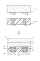
- Fourth Embodiment 7 is a cross-sectional view showing an example of a wiring board according to the fourth embodiment.
- the interlayer connection conductor 22 will be described by dividing it into an inner region 22a and an outer circumferential region 22b, as in Fig. 5.
- the interlayer connection conductor 22 contains a metal component.
- the interlayer connection conductor 22 contains particulate metal.
- the outer peripheral region 22b may have a higher proportion of metal particles than the inner region 22a located inside the outer peripheral region 22b.
- the area excluding the metal particle portion is preferably filled with a resin component.
- the bonding strength between the metals is weak and they are connected by a resin component with a lower elastic modulus than the metal, so stress caused by the difference in thermal expansion coefficient between the interlayer connection conductor 22 and the organic resin base 21 located around it is easily alleviated.
- This makes it possible to reduce the occurrence of problems such as peeling between the interlayer connection conductor 22 and the organic resin base 21 around it. This allows the wiring board 1 to further reduce the decrease in insulation resistance.
- the particulate metal has an aspect ratio of 2 or less when viewed in cross section of the wiring board 1.
- the interlayer connection conductor 22 constituting the wiring board 1 has particulate metal with such an aspect ratio, the binding force within the metal is smaller than in an ingot-like material in which the metal is integrated without gaps.
- the metal located in the inner region 22a may be, for example, in the form of connected metal.
- the inner region 22a may have voids to the extent that the desired conductivity is obtained.
- Fifth Embodiment 8 is a cross-sectional view showing an example of a wiring board according to the fifth embodiment.
- the interlayer connection conductor 22 of the wiring board 1 may have a diameter smaller at a portion 24 close to a second surface 201, which is a surface of the organic resin base 21, than at a portion 23 located at the center in the thickness direction of the organic resin base wiring layer 20.
- the peripheral surface 25 of the interlayer connection conductor 22 facing the organic resin base 21 has a partially rounded shape, the surface area of the interlayer connection conductor 22 is reduced, making it less susceptible to deformation due to external pressure. Even if the organic resin base 21 is significantly deformed, for example, the interlayer connection conductor 22 is likely to only deform to a smaller extent. This makes it possible to improve the connection reliability between the interlayer connection conductor 22 and the external circuit board 4 that is electrically mounted on the interlayer connection conductor 22.
- the diameter of the interlayer connection conductor 22 of the wiring board 1 may be gradually reduced from near the center toward the ends in the thickness direction of the organic resin base 21. This makes it easier for the interlayer connection conductor 22 to undergo a mechanical effect that changes its shape from a polyhedron to a sphere, making the wiring board 1 less susceptible to deformation or destruction.
- the organic resin contained in the organic resin base 21 may, for example, penetrate deeply toward the center in the radial direction of the interlayer connection conductor 22 and surround it. This can further reduce deformation of the interlayer connection conductor 22. As a result, the wiring board 1 is less likely to deform the interlayer connection conductor 22 even when, for example, the external circuit board 4 is connected to the surface (second surface 201) of the organic resin base 21 at high temperature or pressure.
- Embodiments 9 and 10 are cross-sectional views showing another example of the wiring board according to the embodiment.
- the wiring board 1 may have a first surface wiring layer 16, which is a surface wiring layer located on the first surface 101, and a second surface wiring layer 29, which is a surface wiring layer located on the second surface 201.
- the first surface wiring layer 16 and the second surface wiring layer 29 may both have a circular shape in a planar view.
- the diameter of the second surface wiring layer 29 in a planar view may be larger than the diameter of the first surface wiring layer 16 in a planar view.
- the organic resin base 21 has a larger thermal expansion coefficient than the ceramic base 11, so that the dimensional change during heating and cooling is larger.
- the organic resin base wiring layer 20 when the organic resin base wiring layer 20 is connected to the external circuit board 4, even if the position of the second surface wiring layer 29 of the organic resin base wiring layer 20 is misaligned from the position of the corresponding connection pad of the external circuit board 4, electrical connection is easily ensured. It becomes possible to improve the alignment effect of the bonding material (melting metal material such as solder) located between the organic resin base wiring layer 20 and the external circuit board 4.
- the bonding material melting metal material such as solder
- the wiring board 1 may have a conductor layer 13 located inside the ceramic base 11.
- the wiring board 1 may also have a conductor layer 26 located inside the organic resin base 21.
- the thickness of the organic resin base 21 may be, for example, in the range of 0.05 to 0.2 when the thickness of the ceramic base 11 is taken as 1. If the thickness of the organic resin base 21, which has a low elastic modulus, is thinner than the thickness of the ceramic base 11, the ceramic base 11 is less likely to deform even in response to loads such as thermal expansion and weight of the wiring board 1.
- the surface wiring layer 27, which is the copper foil portion, may be entirely embedded in the organic resin base 21. Also, of the second surface wiring layer 29, the plating film 28 portion may entirely protrude from the surface (second surface 201) of the organic resin base 21.
- FIG. 11 is an explanatory diagram showing an example of a method for manufacturing a wiring board according to sample 1.
- a fired ceramic base wiring layer 10 and an uncured organic resin base wiring layer 20 were prepared.
- the ceramic base wiring layer 10 has a copper metallized film 120 on the surface of a glass ceramic insulating base (ceramic base 11).
- the metallized film 120 protrudes from the surface of the insulating base by a thickness close to the thickness of the surface conductor layer 12.
- the uncured organic resin base wiring layer 20 has an uncured interlayer connection conductor 220 that penetrates the uncured organic resin base 21 in the thickness direction.
- the uncured organic resin base 21 was made using a thermosetting epoxy resin as the organic material (resin component).
- the uncured interlayer connection conductor 220 contains 50 mol % copper powder, 25 mol % Sn powder, 25 mol % Bi powder, and the remainder epoxy resin.
- the wiring layer is formed by transferring patterned copper foil (initially attached to a PET film) onto the surface of the uncured organic resin base 21.
- the surface wiring layers formed on the first surface 101 (surface of the ceramic base wiring layer 10) and the second surface 201 (surface of the organic resin base wiring layer 20) of the wiring board 1 are both circular. 64 circular surface wiring layers were formed on each of the first surface 101 and the second surface 201.
- the diameter of the surface wiring layer formed on the first surface 101 was 200 ⁇ m, and the diameter of the surface wiring layer formed on the second surface 201 was 500 ⁇ m.
- the area of each of the surface wiring layers formed on the second surface 201 was ten times the area of each of the surface wiring layers formed on the first surface 101.
- the surface wiring layers of the first surface 101 were arranged in a lattice pattern in the center when the first surface 101 on the ceramic base 11 side was viewed in a plan view.
- the surface wiring layers of the second surface 201 were arranged so as to surround the periphery when the second surface 201 on the organic resin base 21 side was viewed in a plan view. 64 surface wiring layers of the second surface 201 were connected in series.
- the thermal expansion coefficient of the ceramic base 11 (glass ceramics) was 12 ⁇ 10 -6 /K
- the thermal expansion coefficient of the ceramic base wiring layer 10 having a wiring layer was 13 ⁇ 10 -6 /K
- the thermal expansion coefficient of the organic resin base 21 was 30 ⁇ 10 -6 /K
- the thermal expansion coefficient of the organic resin base wiring layer 20 having a wiring layer was 20 ⁇ 10 -6 /K.
- alumina ceramics may be used instead of glass ceramics as the ceramic base 11.
- W, W--Cu, Mo, etc. can be used as the conductor.
- the thermal expansion coefficient of such alumina ceramics is, for example, about 6 ⁇ 10 -6 /K to 8 ⁇ 10 -6 /K.
- the fired ceramic base wiring layer 10 and the uncured organic resin base wiring layer 20 were stacked and pressurized and heated at a temperature of 75°C and a pressure of 3 Pa in a vacuum atmosphere for 15 seconds.
- the uncured organic resin base wiring layer 20 was placed on a base, and the fired ceramic base wiring layer 10 was stacked on top of it, and a pressurized and heated treatment (250°C, 10 MPa, 15 seconds) was performed.
- a pressurized and heated treatment 250°C, 10 MPa, 15 seconds
- the wiring board 1 of sample 1 has a first surface 101 (the surface on the ceramic substrate wiring layer 10 side) which is the mounting surface for the electrical element 2.
- the second surface 201 (the organic resin substrate wiring layer 20 side) is the connection surface with the external circuit board 4.
- the first region 211 of the organic resin base 21 constituting the organic resin base wiring layer 20 overlapping the surface conductor layer 12 is further pressurized compared to the second region 212 other than the first region 211 (where the surface conductor layer 12 of the ceramic base wiring layer 10 exists), and is therefore more dense.
- the prepared samples 1, 2, 3, 4 and 5 had a copper metallized film 120 as a surface conductor layer 12 on the surface of the ceramic base 11.
- the metallized film 120 had a surface conductor layer 12 protruding from the surface of the ceramic base 11, and protruded by a thickness close to the thickness of the surface conductor layer 12.
- the first region 211 of the organic resin base 21 had a lower ratio of the total area of voids than the second region 212, with a difference of 0.5% or more. In this case, voids with a diameter of 0.1 ⁇ m or more were extracted.
- a wiring board 1 was fabricated by reversing the ceramic base wiring layer 10 and the organic resin base wiring layer 20 in the configuration of sample 1.
- Sample 7 A wiring board having a ceramic base 11 with uniform density was also produced as a comparative example by performing the same process as sample 1, except that a ceramic base wiring layer 10 not having a metallized film on the surface of the ceramic base 11 was used. Sample 7 had the same ratio of the total area of voids in the portions corresponding to the first and second regions of the ceramic base insulating base. In this case, the ratio of the total area of voids was considered to be the same when it was within 1%.
- ⁇ Evaluation> 12 is a plan view showing a wiring board according to an experimental example.
- the diameter of the interlayer connection conductors 22 is 100 ⁇ m
- the interval between adjacent interlayer connection conductors 22 is 50 ⁇ m
- a total of 100 interlayer connection conductors 22 are positioned in 10 rows and 10 columns. These interlayer connection conductors 22 are connected in series.
- Temperature cycle test (the fabricated wiring board was soldered onto the surface of an external circuit board (printed circuit board), and the test sample was placed in a thermostatic chamber controlled at temperatures of -40°C and 125°C in an air atmosphere, with each cycle consisting of 15 minutes/15 minutes, and repeated for up to 2,000 cycles.
- test samples were placed in a thermostatic chamber controlled at temperatures of -40°C and 150°C, with each cycle consisting of 30 minutes/30 minutes, and the test samples were subjected to a maximum of 2,000 cycles. (150°C x 30 minutes/30 minutes was also prepared for both the 125°C x 15 minutes/15 minutes case.)
- Samples 1 to 5 and 7 showed no cracks or other breaks at the connection points between the external circuit board even after 2000 cycles, but sample 6 showed breaks in multiple places. These were particularly concentrated in the four corners (four places) of the peripheral arrangement.
- Samples 1 to 5 and 7 showed no cracks or other breaks at the connection points between the external circuit board even after 2000 cycles, but sample 6 showed breaks in multiple places. These were particularly concentrated in the four corners of the peripheral arrangement.
- the number of defective areas in sample 6 was twice as high (8 areas) as when the temperature was between -40°C and 125°C.
- the reduction rate values shown in Figure 13 are the average values for the four locations shown in Figure 12 (between interlayer connection conductors 22-1 and 22-2, between 22-9 and 22-10, between 22-91 and 22-92, and between 22-99 and 22-100).
- Figure 13 shows the evaluation results of the wiring boards according to the experimental examples. As shown in Figure 13, the effect of reducing the decrease in insulation resistance was confirmed in all of the wiring boards 1A according to samples 1 to 5, compared to the wiring board according to sample 7.
- a wiring board includes a base and a conductor, the substrate is a laminate of a ceramic substrate wiring layer and an organic resin substrate wiring layer,
- the organic resin base wiring layer has an organic resin base as an insulating base
- the ceramic substrate wiring layer has a ceramic substrate as an insulating substrate, the organic resin substrate has a higher thermal expansion coefficient than the ceramic substrate;
- a surface of the laminate facing the ceramic substrate is defined as a first surface, and a surface of the laminate facing the organic resin substrate is defined as a second surface, the first surface and the second surface of the laminate facing opposite to each other,
- the conductor has a first terminal group and a second terminal group; the first terminal group is provided on the first surface of the laminate, the second terminal group is provided on the second surface of the laminate, the first surface is a mounting surface for an electric element, The second surface is a surface for connection to an external circuit board.
- the ceramic base when a surface of the ceramic base that is located on the opposite side to the first surface and that is in contact with the organic resin base is defined as a third surface, the ceramic base has a surface conductor layer on the third surface, the surface conductor layer protrudes from the third surface to have a step of a predetermined thickness, the organic resin base has an interlayer connection conductor penetrating in a thickness direction, the surface conductor layer and the interlayer connection conductor are electrically connected to each other, the organic resin base has a first region and a second region, the first region is located on a surface conductor layer; The second region may be located on the organic resin base other than the first region.
- the wiring board of (2) above may have a coated conductor layer located on the surface conductor layer.
- the interlayer connection conductor may have a mixed region near the outer periphery in which the resin component is positioned in a band shape in the longitudinal direction of the interlayer connection conductor and in which a metal is mixed.
- the interlayer connection conductor may have an outer peripheral region and an inner region located inside the outer peripheral region, and the outer peripheral region may have a higher proportion of the particulate metal than the inner region.
- the interlayer connection conductor may have a smaller diameter at a portion closer to the surface of the organic resin base than at a portion located at the center of the thickness direction of the organic resin base.
- an electric device includes a wiring board according to any one of (1) to (7) above, and an electrical device mounted on the first surface.
- an electric device structure includes the electric device according to (8) above, and an external circuit board connected to the second surface.
Landscapes
- Engineering & Computer Science (AREA)
- Microelectronics & Electronic Packaging (AREA)
- Manufacturing & Machinery (AREA)
- Production Of Multi-Layered Print Wiring Board (AREA)
Priority Applications (1)
| Application Number | Priority Date | Filing Date | Title |
|---|---|---|---|
| JP2024571803A JPWO2024154790A1 (https=) | 2023-01-19 | 2024-01-18 |
Applications Claiming Priority (2)
| Application Number | Priority Date | Filing Date | Title |
|---|---|---|---|
| JP2023006887 | 2023-01-19 | ||
| JP2023-006887 | 2023-04-03 |
Publications (1)
| Publication Number | Publication Date |
|---|---|
| WO2024154790A1 true WO2024154790A1 (ja) | 2024-07-25 |
Family
ID=91956231
Family Applications (1)
| Application Number | Title | Priority Date | Filing Date |
|---|---|---|---|
| PCT/JP2024/001321 Ceased WO2024154790A1 (ja) | 2023-01-19 | 2024-01-18 | 配線基板、電気装置および電気装置構造体 |
Country Status (2)
| Country | Link |
|---|---|
| JP (1) | JPWO2024154790A1 (https=) |
| WO (1) | WO2024154790A1 (https=) |
Citations (3)
| Publication number | Priority date | Publication date | Assignee | Title |
|---|---|---|---|---|
| JPH07170046A (ja) * | 1993-09-22 | 1995-07-04 | Matsushita Electric Ind Co Ltd | プリント配線板及びその製造方法 |
| JP2005235808A (ja) * | 2004-02-17 | 2005-09-02 | Murata Mfg Co Ltd | 積層型電子部品およびその製造方法 |
| JP2011071315A (ja) * | 2009-09-25 | 2011-04-07 | Shinko Electric Ind Co Ltd | 配線基板及び配線基板の製造方法 |
-
2024
- 2024-01-18 WO PCT/JP2024/001321 patent/WO2024154790A1/ja not_active Ceased
- 2024-01-18 JP JP2024571803A patent/JPWO2024154790A1/ja active Pending
Patent Citations (3)
| Publication number | Priority date | Publication date | Assignee | Title |
|---|---|---|---|---|
| JPH07170046A (ja) * | 1993-09-22 | 1995-07-04 | Matsushita Electric Ind Co Ltd | プリント配線板及びその製造方法 |
| JP2005235808A (ja) * | 2004-02-17 | 2005-09-02 | Murata Mfg Co Ltd | 積層型電子部品およびその製造方法 |
| JP2011071315A (ja) * | 2009-09-25 | 2011-04-07 | Shinko Electric Ind Co Ltd | 配線基板及び配線基板の製造方法 |
Also Published As
| Publication number | Publication date |
|---|---|
| JPWO2024154790A1 (https=) | 2024-07-25 |
Similar Documents
| Publication | Publication Date | Title |
|---|---|---|
| KR100921643B1 (ko) | 전자부품 | |
| US7851708B2 (en) | Composite substrate and method for manufacturing composite substrate | |
| US7180007B2 (en) | Electronic circuit device and its manufacturing method | |
| JP4821849B2 (ja) | 複合基板及び複合基板の製造方法 | |
| JP4404139B2 (ja) | 積層型基板、電子装置および積層型基板の製造方法 | |
| JP2001076957A (ja) | セラミック電子部品 | |
| US7820916B2 (en) | Composite ceramic substrate | |
| US7656677B2 (en) | Multilayer electronic component and structure for mounting multilayer electronic component | |
| US5576518A (en) | Via-structure of a multilayer interconnection ceramic substrate | |
| EP4407672A1 (en) | Metal-ceramic bonding substrate, and method for manufacturing same | |
| JP3336240B2 (ja) | 半導体素子実装基板 | |
| JP2003197460A (ja) | 電子部品の製造方法および電子部品 | |
| JP5535451B2 (ja) | セラミック配線基板およびその製造方法 | |
| WO2024154790A1 (ja) | 配線基板、電気装置および電気装置構造体 | |
| JPH10116706A (ja) | チップ型サーミスタ及びその製造方法 | |
| JP3842478B2 (ja) | 半導体素子実装配線基板の実装構造 | |
| JP4158798B2 (ja) | 複合セラミック基板 | |
| WO2024154834A1 (ja) | 電子素子搭載用基板 | |
| WO2018074188A1 (ja) | インダクタ部品、インダクタ部品の製造方法 | |
| WO2023003024A1 (ja) | 配線基板 | |
| JP4788581B2 (ja) | 複合基板 | |
| JP2003017838A (ja) | 多層基板 | |
| JP2000022023A (ja) | 接続構造体とその製造方法、及び実装構造体 | |
| JPH11274372A (ja) | 半導体装置及びその半導体パッケージ | |
| JP3250166B2 (ja) | 積層複合電子部品 |
Legal Events
| Date | Code | Title | Description |
|---|---|---|---|
| 121 | Ep: the epo has been informed by wipo that ep was designated in this application |
Ref document number: 24744710 Country of ref document: EP Kind code of ref document: A1 |
|
| ENP | Entry into the national phase |
Ref document number: 2024571803 Country of ref document: JP Kind code of ref document: A |
|
| WWE | Wipo information: entry into national phase |
Ref document number: 2024571803 Country of ref document: JP |
|
| NENP | Non-entry into the national phase |
Ref country code: DE |
|
| 122 | Ep: pct application non-entry in european phase |
Ref document number: 24744710 Country of ref document: EP Kind code of ref document: A1 |