WO2024154487A1 - 電源制御装置、スイッチング電源 - Google Patents
電源制御装置、スイッチング電源 Download PDFInfo
- Publication number
- WO2024154487A1 WO2024154487A1 PCT/JP2023/044594 JP2023044594W WO2024154487A1 WO 2024154487 A1 WO2024154487 A1 WO 2024154487A1 JP 2023044594 W JP2023044594 W JP 2023044594W WO 2024154487 A1 WO2024154487 A1 WO 2024154487A1
- Authority
- WO
- WIPO (PCT)
- Prior art keywords
- power supply
- voltage
- signal
- temperature characteristic
- error signal
- Prior art date
- Legal status (The legal status is an assumption and is not a legal conclusion. Google has not performed a legal analysis and makes no representation as to the accuracy of the status listed.)
- Ceased
Links
Images





Classifications
-
- H—ELECTRICITY
- H02—GENERATION; CONVERSION OR DISTRIBUTION OF ELECTRIC POWER
- H02M—APPARATUS FOR CONVERSION BETWEEN AC AND AC, BETWEEN AC AND DC, OR BETWEEN DC AND DC, AND FOR USE WITH MAINS OR SIMILAR POWER SUPPLY SYSTEMS; CONVERSION OF DC OR AC INPUT POWER INTO SURGE OUTPUT POWER; CONTROL OR REGULATION THEREOF
- H02M3/00—Conversion of DC power input into DC power output
- H02M3/02—Conversion of DC power input into DC power output without intermediate conversion into AC
- H02M3/04—Conversion of DC power input into DC power output without intermediate conversion into AC by static converters
- H02M3/10—Conversion of DC power input into DC power output without intermediate conversion into AC by static converters using discharge tubes with control electrode or semiconductor devices with control electrode
- H02M3/145—Conversion of DC power input into DC power output without intermediate conversion into AC by static converters using discharge tubes with control electrode or semiconductor devices with control electrode using devices of a triode or transistor type requiring continuous application of a control signal
- H02M3/155—Conversion of DC power input into DC power output without intermediate conversion into AC by static converters using discharge tubes with control electrode or semiconductor devices with control electrode using devices of a triode or transistor type requiring continuous application of a control signal using semiconductor devices only
Definitions
- This disclosure relates to a power supply control device and a switching power supply.
- a known method for increasing the current supply capacity of a switching power supply is the stack method (or multi-phase method), in which multiple switch output stages connected in parallel are driven with a specified phase difference. With this driving method, it is ideal for the magnitude of the inductor current flowing through the inductors of each switch output stage to be the same.
- Patent Document 1 As an example of related prior art, Patent Document 1 can be mentioned.
- the magnitude of the inductor currents in each switch output stage may not match, resulting in a current imbalance. If this occurs, the output current of the switching power supply may become biased, which may lead to a decrease in efficiency. Furthermore, if the current balance is relatively significantly disrupted, the protection circuit may be activated and the switching power supply may malfunction (for example, the output operation may be forcibly stopped).
- the power supply control device disclosed in this specification is a power supply control device configured to control the drive of a switch output stage that generates an output voltage from an input voltage, and includes a feedback control circuit configured to determine the duty ratio of the switch output stage according to an error signal between a feedback voltage corresponding to the output voltage and a predetermined reference voltage, and a temperature characteristic applying circuit configured to give a negative temperature characteristic to the conversion coefficient from the error signal to the duty ratio.
- This disclosure makes it possible to provide a stack-type switching power supply that is less likely to lose current balance.
- FIG. 1 is a diagram showing a comparative example of a switching power supply.
- FIG. 2 is a diagram showing how the current balance is lost in the comparative example.
- FIG. 3 is a diagram showing a first embodiment of a switching power supply.
- FIG. 4 is a diagram showing how the current balance is improved in the first embodiment.
- FIG. 5 is a diagram showing a second embodiment of a switching power supply.
- FIG. 6 is a diagram showing an example of the thermal equilibrium current balance control.
- FIG. 7 is a diagram showing the inductor current without thermal balance current balance control.
- FIG. 8 is a diagram showing the inductor current with the thermal equilibrium current balance control.
- FIG. 9 is a diagram showing a third embodiment of a switching power supply.
- FIG. 10 is a diagram showing a fourth embodiment of a switching power supply.
- FIG. 11 is a diagram showing a fifth embodiment of a switching power supply.
- a switching power supply Y of this comparative example has semiconductor devices Y1 and Y2, inductors L1 and L2, and capacitors C1 and C2.
- the semiconductor device Y1 is connected to the application terminal of the input voltage Vi and the ground terminal.
- the output terminal of the semiconductor device Y1 is connected to the first terminal of the inductor L1.
- the second terminal of the inductor L1 is commonly connected to the first terminal of the capacitor C1 and the application terminal of the output voltage Vo.
- the second terminal of the capacitor C1 is connected to the ground terminal.
- the semiconductor device Y1, inductor L1, and capacitor C1 form a step-down switch output stage that generates a switch voltage Vst1 from an input voltage Vi and rectifies and smoothes the switch voltage Vst1.
- the semiconductor device Y1 controls the switching of the inductor current IL1 flowing through the inductor L1 based on a clock signal (not shown) generated inside the semiconductor device Y1.
- the semiconductor device Y2 is connected to the application terminal of the input voltage Vi and the ground terminal.
- the output terminal of the semiconductor device Y2 is connected to the first terminal of the inductor L2.
- the second terminal of the inductor L2 is commonly connected to the first terminal of the capacitor C2 and the application terminal of the output voltage Vo.
- the second terminal of the capacitor C2 is connected to the ground terminal.
- the semiconductor device Y2, inductor L1, and capacitor C2 form a step-down switch output stage that generates a switch voltage Vst2 from the input voltage Vi and rectifies and smoothes the switch voltage Vst2.
- the semiconductor device Y2 controls the switching of the inductor current IL2 flowing through the inductor L2 based on a clock signal (not shown) generated inside the semiconductor device Y2.
- a load Z is connected to the output terminal of the output voltage Vo.
- An output current Io flows through the load Z according to the output voltage Vo and the resistance value of the load Z.
- the switching power supply Y includes semiconductor devices Y1 and Y2 as means for driving and controlling each of the multiple switch output stages whose outputs are common.
- Figure 2 shows how the current balance is lost in the switching power supply Y of this comparative example.
- this figure depicts, from the top, inductor currents IL1 (dashed line) and IL2 (solid line), switch voltage Vst1, and switch voltage Vst2.
- the average value A1 of the inductor current IL1 and the average value A2 of the inductor current IL2 are approximately equal.
- the average value A1 of the inductor current IL1 and the average value A2 of the inductor current IL2 may not match, i.e., the current balance may be lost.
- the protection circuit may be activated and the switching power supply Y may enter a malfunction state (for example, a state in which the output operation is forcibly stopped).
- ⁇ Switching power supply (first embodiment)> 3 is a diagram showing a first embodiment of a switching power supply.
- the switching power supply X of this embodiment is based on the above-mentioned comparative example (FIG. 1) and includes semiconductor devices X1 and X2 instead of the semiconductor devices Y1 and Y2.
- the semiconductor devices X1 and X2 are each a power supply control device (a so-called power supply control IC [integrated circuit]) configured to drive and control a plurality of switch output stages that generate an output voltage Vo from an input voltage Vi.
- a power supply control device a so-called power supply control IC [integrated circuit]
- semiconductor devices X1 and X2 each form multiple switch output stages together with external discrete components (inductors L1 and L2, and capacitors C1 and C2).
- the semiconductor devices X1 and X2 use common internal signals (e.g., a common error signal Vc and a common clock signal CLK) in their output feedback control.
- the common error signal Vc may be a voltage signal or a current signal corresponding to the difference between the output voltage Vo and a desired target value.
- the common clock signal CLK may be a square wave signal pulse-driven at a predetermined switching frequency fsw.
- Semiconductor devices X1 and X2 are the same model with a common circuit configuration, and can be switched between master and slave by register settings, etc.
- semiconductor device X1 is the master and semiconductor device X2 is the slave.
- semiconductor device X1 internally generates error signal Vc1 and clock signal CLK1, and performs output feedback control using error signal Vc1 and clock signal CLK1.
- semiconductor device X1 determines the duty ratio of switch voltage Vst1 according to error signal Vc1 and clock signal CLK1.
- Semiconductor device X1 also outputs error signal Vc1 and clock signal CLK1 to semiconductor device X2 as the aforementioned common error signal Vc and common clock signal CLK.
- semiconductor device X2 does not internally generate error signal Vc2 and clock signal CLK2, but instead accepts the input of common error signal Vc and common clock signal CLK output from semiconductor device X1, and performs output feedback control using the common error signal Vc and common clock signal CLK (corresponding to error signal Vc1 and clock signal CLK1). In other words, semiconductor device X2 determines the duty ratio of switch voltage Vst2 according to the common error signal Vc and common clock signal CLK.
- a third or more power supply control devices may be provided.
- one of the multiple power supply control devices is set as the master, and the rest are set as slaves.
- FIG. 4 is a diagram showing how the current balance is improved in the switching power supply X of the first embodiment.
- the inductor currents IL1 dashed line
- IL2 solid line
- the switch voltage Vst1 the switch voltage Vst2 are depicted from the top.
- the semiconductor devices X1 and X2 share a common error signal Vc and a common clock signal CLK (for example, the error signal Vc1 and clock signal CLK1 generated internally in the semiconductor device X1).
- output feedback control is performed so that the duty ratios of the switch voltages Vst1 and Vst2 match in response to the common error signal Vc and the common clock signal CLK.
- the current balance of the inductor currents IL1 and IL2 is adjusted, improving the efficiency of the switching power supply X.
- Methods for further improving the current balance of the switching power supply X include so-called active compensation and passive compensation.
- the current balance is improved by improving the accuracy of the feedback control circuit that determines the duty ratio of each of the switch voltages Vst1 and Vst2 according to the common error signal Vc and the common clock signal CLK.
- this method requires a high-precision trimming circuit.
- this method has difficulty in correcting the DCR [direct current resistance] variations of the inductors L1 and L2 and the on-resistance variations of the power transistors that form the switch output stage.
- semiconductor devices X1 and X2 are separate, independent devices. Therefore, thermal balance between them can be important.
- ⁇ Switching Power Supply (Second Embodiment)> 5 is a diagram showing a second embodiment of a switching power supply.
- the switching power supply X of this embodiment is based on the first embodiment (FIG. 3) described above, and illustrates a more specific example of the internal configuration of a semiconductor device X1.
- the semiconductor device X1 includes an output transistor M1, a synchronous rectifier transistor M2, a feedback control circuit 100, and a temperature characteristic providing circuit 200.
- the output transistor M1 corresponds to the upper switch of the half bridge.
- the output transistor M1 may be an NMOSFET [N-channel type metal oxide semiconductor field effect transistor].
- the drain of the output transistor M1 is connected to the application terminal of the input voltage Vi.
- the source of the output transistor M1 is connected to the application terminal of the switch voltage Vst1.
- the gate of the output transistor M1 is connected to the application terminal of the upper gate signal HG.
- the output transistor M1 is in the on state when the upper gate signal HG is at a high level, and in the off state when the upper gate signal HG is at a low level.
- the synchronous rectifier transistor M2 corresponds to the lower switch of the half bridge.
- the synchronous rectifier transistor M2 may be an NMOSFET.
- the drain of the synchronous rectifier transistor M2 is connected to the application terminal of the switch voltage Vst1.
- the gate of the synchronous rectifier transistor M2 is connected to the application terminal of the lower gate signal LG.
- the synchronous rectifier transistor M2 is in the ON state when the lower gate signal LG is at a high level, and in the OFF state when the lower gate signal LG is at a low level.
- the output transistor M1 and the synchronous rectifier transistor M2 are complementarily turned on/off in response to the upper gate signal HG and the lower gate signal LG. This on/off operation generates a square-wave switch voltage Vst1 at the first end of the inductor L1 that is pulse-driven between the input voltage Vi and the ground voltage GND.
- the term "complementary" above includes cases where the on/off states of the output transistor M1 and the synchronous rectifier transistor M2 are completely reversed, as well as cases where a period of time (dead time) during which both transistors are simultaneously off is provided.
- the rectification method of the switch output stage SW1 is not limited to the above-mentioned synchronous rectification method, and may be a diode rectification method using a rectifier diode as the lower switch.
- the output transistor M1 may be replaced with a PMOSFET.
- the output transistor M1 and the synchronous rectification transistor M2 may be externally attached to the semiconductor device X1.
- high-voltage elements such as power MOSFETs, IGBTs [insulated gate bipolar transistors], and SiC transistors as the output transistor M1 and the synchronous rectifier transistor M2, respectively.
- high-voltage elements such as power MOSFETs, IGBTs [insulated gate bipolar transistors], and SiC transistors
- GaN devices may be used as the output transistor M1 and the synchronous rectifier transistor M2, respectively.
- the feedback control circuit 100 determines the duty ratio Don1 of the switch output stage SW1 according to the error signal Vc1 between the feedback voltage Vfb corresponding to the output voltage Vo and a predetermined reference voltage Vref.
- the feedback control circuit 100 includes an error amplifier 101, an oscillator 102, a ramp signal generating circuit 103, a current detection circuit 104, a signal summing circuit 105, a comparator 106, a controller 107, and a driver 108.
- the error signal Vc1 rises when the feedback voltage Vfb is lower than the reference voltage Vref, and falls when the feedback voltage Vfb is higher than the reference voltage Vref.
- the feedback voltage Vfb may be, for example, a divided voltage of the output voltage Vo. If the output voltage Vo is within the input dynamic range of the error amplifier 101, the output voltage Vo may be directly input to the error amplifier 101 as the feedback voltage Vfb.
- the reference voltage Vref may be, for example, a bandgap voltage with a relatively flat temperature characteristic.
- the ramp signal Vr1 starts to rise from a zero value when the output transistor M1 is turned on, and is reset to a zero value when the output transistor M1 is turned off.
- the current detection circuit 104 detects the inductor current IL1 (hereinafter referred to as the upper inductor current IL1H) flowing through the switch output stage SW1 during the on-period Ton1 of the output transistor M1, for example, and generates a current detection signal Vcs1 (corresponding to current feedback information).
- the inductor current IL1 hereinafter referred to as the upper inductor current IL1H
- Vcs1 current detection signal
- the upper inductor current IL1H may be detected by any method.
- the drain-source voltage of the output transistor M1 may be detected, or the voltage across a sense resistor connected in series to the output transistor M1 may be detected.
- the drain-source voltage of a current detection transistor connected in parallel to the output transistor M1 may be detected.
- the signal summing circuit 105 adds the ramp signal Vr1 and the current detection signal Vcs1 to generate the slope signal SLP1.
- Comparator 106 generates a comparison signal CMP1 (corresponding to an off signal) by comparing the error signal Vc1 input to the inverting input terminal (-) - more precisely, an offset error signal (Vc1+Vf1) obtained by adding the forward drop voltage Vf1 of diode 201 to the error signal Vc1 - with the slope signal SLP1 input to the non-inverting input terminal (+). This comparison process determines the off timing of output transistor M1.
- the comparison signal CMP1 is at a high level when SLP1 ⁇ Vc1+Vf1, and is at a low level when SLP1>Vc1+Vf1. In other words, the pulse generation timing of the comparison signal CMP1 becomes slower as the offset error signal (Vc1+Vf1) becomes higher, and becomes faster as the offset error signal (Vc1+Vf1) becomes lower.
- the duty ratio Don1 Ton1/Tsw1 of the switch output stage SW1 becomes larger as the offset error signal (Vc1 + Vf1) becomes higher, and conversely, becomes smaller as the offset error signal (Vc1 + Vf1) becomes lower.
- the controller 107 determines the duty ratio Don1 in accordance with the clock signal CLK1 and the comparison signal CMP1.
- the driver 108 generates an upper gate signal HG and a lower gate signal LG in response to the pulse width modulation signal PWM. For example, when the pulse width modulation signal PWM is at a high level, the driver 108 sets the upper gate signal HG to a high level and the lower gate signal LG to a low level. On the other hand, when the pulse width modulation signal PWM is at a low level, the driver 108 sets the upper gate signal HG to a low level and the lower gate signal LG to a high level.
- the semiconductor device X1 also includes a temperature characteristic applying circuit 200.
- the temperature characteristic applying circuit 200 imparts a negative temperature characteristic to the conversion coefficient from the error signal Vc1 to the duty ratio Don1.
- the duty ratio Don1 becomes smaller as the temperature of the semiconductor device X1 increases and becomes larger as the temperature of the semiconductor device X1 decreases.
- the temperature of the semiconductor device X1 may be, for example, the junction temperature in the element formation region of the output transistor M1.
- the temperature characteristic applying circuit 200 includes a diode 201.
- the forward drop voltage Vf1 of the diode 201 has a negative temperature characteristic. That is, the higher the temperature of the semiconductor device X1, the lower the forward drop voltage Vf1 becomes, and the lower the temperature of the semiconductor device X1, the higher the forward drop voltage Vf1 becomes. Therefore, if the error signal Vc1 is assumed to be a fixed value, the offset error signal (Vc1+Vf1) becomes lower the higher the temperature of the semiconductor device X1, and the lower the temperature of the semiconductor device X1, the higher the offset error signal (Vc1+Vf1) becomes.
- the intersection timing between the offset error signal (Vc1+Vf1) and the slope signal SLP1 becomes earlier as the temperature of the semiconductor device X1 increases, and becomes later as the temperature of the semiconductor device X1 decreases.
- the above intersection timing corresponds to the off timing of the output transistor M1. Therefore, the duty ratio Don1 of the switch output stage SW1 becomes smaller as the temperature of the semiconductor device X1 increases, and becomes larger as the temperature of the semiconductor device X1 decreases.
- the temperature of the semiconductor device X1 increases as the inductor current IL1 flowing through the switch output stage SW1 increases, and decreases as the inductor current IL1 decreases. Therefore, when the inductor current IL1 increases and the temperature of the semiconductor device X1 rises, the duty ratio Don1 is reduced by the action of the temperature characteristic imparting circuit 200 described above. Conversely, when the inductor current IL1 decreases and the temperature of the semiconductor device X1 drops, the duty ratio Don1 is increased by the action of the temperature characteristic imparting circuit 200. As a result, the inductor current IL1 converges to a predetermined equilibrium state.
- the semiconductor device X2 that controls the drive of the switch output stage SW2 is the same model as the semiconductor device X1, and the internal configurations of the two are the same. Therefore, duplicated explanations will be omitted.
- this diagram illustrates an example in which the semiconductor device X1 is the master and the semiconductor device X2 is the slave.
- the semiconductor device X1 outputs the error signal Vc1 and the clock signal CLK1 to the semiconductor device X2 as the aforementioned common error signal Vc and common clock signal CLK.
- the error amplifier and oscillator (neither shown) of the semiconductor device X2 are both disabled (non-operating).
- thermo balance current balance control this type of balance control is referred to as "thermal balance current balance control.”
- FIG. 6 is a diagram showing an example of thermal equilibrium current balance control realized by introducing a temperature characteristic applying circuit 200. From the top, the diagram depicts switch voltages Vst1 and Vst2, inductor currents IL1 (solid line) and IL2 (dashed line), and slope signals SLP1 (solid line) and SLP2 (dashed line). In addition, the forward drop voltages of diodes 201 provided in semiconductor devices X1 and X2 are distinguished as Vf1 and Vf2.
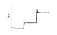
- Figures 7 and 8 are both diagrams showing the behavior of inductor currents IL1 (solid line) and IL2 (dashed line) associated with a gradual increase in output current Io (small ⁇ medium ⁇ large).
- the behavior in each diagram is the result of a simulation in which a stack-type switching power supply 1 is constructed using semiconductor devices X1 and X2 whose characteristics are intentionally shifted from each other.
- Figure 7 shows the behavior when the aforementioned thermal balance current balance control is not implemented.
- Figure 8 shows the behavior when the aforementioned thermal balance current balance control is implemented.
- the current balance of the inductor currents IL1 and IL2 is improved by introducing thermal equilibrium current balance control.
- ⁇ Switching power supply (third embodiment)> 9 is a diagram showing a third embodiment of a switching power supply.
- the switching power supply X of this embodiment is based on the second embodiment (FIG. 5) described above, but has a modified circuit configuration of the temperature characteristic applying circuit 200.
- the comparator 106 is changed from a two-input type to a four-input type.
- the temperature characteristic applying circuit 200 includes a digital/analog conversion circuit 202 instead of the previously mentioned diode 201, and resistors 203 and 204 (resistance values: R203 and R204).
- the digital/analog conversion circuit 202 converts the digital trimming signal TRIM into an analog first voltage signal V1.
- the first voltage signal V1 may be an intermediate voltage between the reference voltage Vref and the ground voltage GND. If the temperature characteristic of the reference voltage Vref is flat, the temperature characteristic of the first voltage signal V1 will also be flat.
- resistors 203 and 204 are a combination of multiple types of resistors with different temperature characteristics.
- the resistance value R203 of resistor 203 may have a positive temperature characteristic.
- the resistance value R204 of resistor 204 may have a negative temperature characteristic.
- the second voltage signal V2 has a negative temperature characteristic.
- an implant resistor diffuseused resistor
- a polysilicon resistor may be used as the resistor with the negative temperature characteristic.
- the four-input comparator 106 generates a comparison signal CMP1 by comparing the first sum signal (SLP1+V1) between the non-inverting input terminals (+) with the second sum signal (Vc1+V2) between the inverting input terminals (-).
- the comparison signal CMP1 becomes high level when the first sum signal (SLP1+V1) is higher than the second sum signal (Vc1+V2).
- the comparison signal CMP1 becomes low level when the first sum signal (SLP1+V1) is lower than the second sum signal (Vc1+V2).
- the temperature characteristic applying circuit 200 applies the input offset voltage Vofs having a negative temperature characteristic to the comparator 106.
- the input offset voltage Vofs (and therefore the second voltage signal V2) may have a positive temperature characteristic.
- the first voltage signal V1 is input to the inverting input terminal (-) of the comparator 106
- the second voltage signal V2 is input to the non-inverting input terminal (+) of the comparator 106.
- ⁇ Switching Power Supply (Fourth Embodiment)> 10 is a diagram showing a fourth embodiment of a switching power supply.
- the switching power supply X of this embodiment is based on the third embodiment (FIG. 9) described above, but the circuit configuration of the temperature characteristic applying circuit 200 is modified.
- the temperature characteristic applying circuit 200 includes a PTAT [proportional to absolute temperature] voltage source 205 in place of the previously mentioned components 202 to 204.
- the PTAT voltage source 205 outputs a PTAT voltage proportional to absolute temperature.
- the temperature characteristic applying circuit 200 uses this PTAT voltage source 205 to set the input offset voltage Vofs. Note that the circuit configuration of the PTAT voltage source 205 can be achieved by applying well-known technology.
- Fig. 11 is a diagram showing a fifth embodiment of a switching power supply.
- the switching power supply X of this embodiment is based on the second embodiment (Fig. 5) described above, but has a modified circuit configuration of the temperature characteristic applying circuit 200.
- this diagram clearly shows the circuit configuration of the ramp signal generating circuit 103.
- the temperature characteristic applying circuit 200 includes a resistor 206 (resistance value: R206) instead of the previously mentioned diode 201.
- the ramp signal generating circuit 103 also includes a current source 103a, a capacitor 103b, and a switch 103c.
- the first terminal of the current source 103a is connected to the power supply terminal.
- the second terminal of the current source 103a and the first terminals of the resistor 206 and the switch 103c are connected to the application terminal of the ramp signal Vr1.
- the second terminal of the resistor 206 is connected to the first terminal of the capacitor 103b.
- the second terminals of the capacitor 103b and the switch 103c are connected to the ground terminal.
- Current source 103a generates a predetermined reference current Iref.
- Capacitor 103b is charged by the reference current Iref when switch 103c is in the off state.
- Switch 103c is turned on/off in response to, for example, the aforementioned pulse width modulation signal PWM.
- switch 103c is turned off when pulse width modulation signal PWM is at a high level. At this time, capacitor 103b is charged by reference current Iref, so ramp signal Vr1 rises. On the other hand, switch 103c is turned on when pulse width modulation signal PWM is at a low level. At this time, capacitor 103b is discharged, so ramp signal Vr1 is reset to zero.
- the resistance value R206 of resistor 206 has a positive temperature characteristic.
- an offset having a positive temperature characteristic is applied to ramp signal Vr1 (and therefore slope signal SLP1).
- This configuration is equivalent to a configuration in which an offset having a negative temperature characteristic is applied to error signal Vc1.
- the power supply control device disclosed in this specification is configured to control the drive of a switch output stage that generates an output voltage from an input voltage, and is configured (first configuration) to include a feedback control circuit configured to determine the duty ratio of the switch output stage according to an error signal between a feedback voltage corresponding to the output voltage and a predetermined reference voltage, and a temperature characteristic imparting circuit configured to impart a negative temperature characteristic to the conversion coefficient from the error signal to the duty ratio.
- the feedback control circuit may be configured (second configuration) to include an error amplifier configured to generate the error signal according to the difference between the feedback voltage and the reference voltage, a comparator configured to compare the error signal with a slope signal to generate a comparison signal, and a controller configured to determine the duty ratio according to a clock signal and the comparison signal.
- the temperature characteristic applying circuit may include a diode whose forward drop voltage has a negative temperature characteristic, and the forward drop voltage may be added to the error signal (third configuration).
- the temperature characteristic applying circuit may be configured to apply an input offset voltage having a negative or positive temperature characteristic to the comparator (fourth configuration).
- the temperature characteristic applying circuit may be configured (fifth configuration) to set the input offset voltage using a resistor ladder that combines multiple types of resistors with different temperature characteristics.
- the temperature characteristic applying circuit may be configured to set the input offset voltage using a PTAT voltage source (sixth configuration).
- the temperature characteristic applying circuit may include a resistor whose resistance value has a positive temperature characteristic, and the voltage across the resistor may be added to the slope signal (seventh configuration).
- the feedback control circuit may further include a ramp signal generating circuit configured to generate a ramp signal, a current detection circuit configured to generate a current detection signal corresponding to the inductor current flowing through the switch output stage, and a signal adding circuit configured to add the ramp signal and the current detection signal to generate the slope signal (eighth configuration).
- the switching power supply disclosed in this specification includes a plurality of switch output stages with a common output, and a plurality of power supply control devices configured to control the drive of each of the plurality of switch output stages, and each of the plurality of power supply control devices is configured to be a power supply control device having any one of the above-mentioned first to eighth configurations (ninth configuration).
- the multiple power supply control devices may be configured such that one is a master and the rest are slaves, the master internally generates the error signal, determines the duty ratio according to the error signal, and outputs the error signal to the slave as a common error signal, and the slave determines the duty ratio according to the common error signal output from the master (tenth configuration).
Landscapes
- Engineering & Computer Science (AREA)
- Power Engineering (AREA)
- Dc-Dc Converters (AREA)
Abstract
電源制御装置10は、入力電圧Viから出力電圧Voを生成するスイッチ出力段SW1の駆動制御を行う。電源制御装置10は、出力電圧Voに応じた帰還電圧Vfbと所定の基準電圧Vrefとの誤差信号Vc1に応じてスイッチ出力段SW1のデューティ比Don1を決定する帰還制御回路100と、誤差信号Vc1からデューティ比Don1への変換係数に負の温度特性を持たせる温度特性付与回路200と、を備える。
Description
本開示は、電源制御装置及びスイッチング電源に関する。
スイッチング電源の電流供給能力を高めるための手法として、並列接続された複数のスイッチ出力段を所定の位相差で駆動させるスタック方式(又はマルチフェイズ方式)が知られている。この駆動方式では、各スイッチ出力段のインダクタにそれぞれ流れるインダクタ電流の大きさが一致していることが理想的である。
なお、上記に関連する従来技術の一例としては、特許文献1を挙げることができる。
しかしながら、例えば、各スイッチ出力段、これらを駆動するドライバ、又は、ドライバを制御する制御回路等の特性のばらつきによって、各スイッチ出力段のインダクタ電流の大きさが一致せず、電流バランスの崩れた状態となり得る。このような状態に陥ると、スイッチング電源の出力電流が偏った動作となり、効率の低下に繋がるおそれがある。また、比較的大きく電流バランスが崩れてしまった場合には、保護回路が働いてスイッチング電源が動作不良状態(例えば強制的に出力動作が停止された状態)となり得る。
例えば、本明細書中に開示されている電源制御装置は、入力電圧から出力電圧を生成するスイッチ出力段の駆動制御を行うように構成された電源制御装置であって、前記出力電圧に応じた帰還電圧と所定の基準電圧との誤差信号に応じて前記スイッチ出力段のデューティ比を決定するように構成された帰還制御回路と、前記誤差信号から前記デューティ比への変換係数に負の温度特性を持たせるように構成された温度特性付与回路とを備える。
なお、その他の特徴、要素、ステップ、利点、及び、特性については、以下に続く発明を実施するための形態及びこれに関する添付の図面によって、さらに明らかとなる。
本開示によれば、電流バランスが崩れにくいスタック方式のスイッチング電源を提供することが可能となる。
<スイッチング電源(比較例)>
図1は、スイッチング電源の比較例(=後出の実施形態と対比される一般的な構成例)を示す図である。本比較例のスイッチング電源Yは、半導体装置Y1及びY2と、インダクタL1及びL2と、キャパシタC1及びC2と、を有する。
図1は、スイッチング電源の比較例(=後出の実施形態と対比される一般的な構成例)を示す図である。本比較例のスイッチング電源Yは、半導体装置Y1及びY2と、インダクタL1及びL2と、キャパシタC1及びC2と、を有する。
半導体装置Y1は、入力電圧Viの印加端と接地端に接続されている。半導体装置Y1の出力端は、インダクタL1の第1端に接続されている。インダクタL1の第2端は、キャパシタC1の第1端と出力電圧Voの印加端に共通に接続されている。キャパシタC1の第2端は、接地端に接続されている。
半導体装置Y1、インダクタL1及びキャパシタC1は、入力電圧Viからスイッチ電圧Vst1を生成し、スイッチ電圧Vst1を整流及び平滑する降圧型のスイッチ出力段を形成している。半導体装置Y1は、その内部で生成されるクロック信号(図示省略)に基づいて、インダクタL1に流れるインダクタ電流IL1をスイッチング制御する。
半導体装置Y2は、入力電圧Viの印加端と接地端に接続されている。半導体装置Y2の出力端は、インダクタL2の第1端に接続されている。インダクタL2の第2端は、キャパシタC2の第1端と出力電圧Voの印加端に共通に接続されている。キャパシタC2の第2端は、接地端に接続されている。
半導体装置Y2、インダクタL1及びキャパシタC2は、入力電圧Viからスイッチ電圧Vst2を生成し、スイッチ電圧Vst2を整流及び平滑する降圧型のスイッチ出力段を形成している。半導体装置Y2は、その内部で生成されるクロック信号(図示省略)に基づいて、インダクタL2に流れるインダクタ電流IL2をスイッチング制御する。
出力電圧Voの出力端には負荷Zが接続されている。負荷Zには、出力電圧Voと負荷Zの抵抗値に応じた出力電流Ioが流れる。
このように、スイッチング電源Yは、出力が共通化された複数のスイッチ出力段それぞれを駆動制御する手段として半導体装置Y1及びY2を備える。
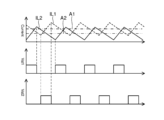
図2は、本比較例のスイッチング電源Yにおいて、電流バランスが崩れる様子を示す図である。特に、本図では、上から順番に、インダクタ電流IL1(破線)及びIL2(実線)、スイッチ電圧Vst1、並びに、スイッチ電圧Vst2が描写されている。
スイッチング電源Yでは、インダクタ電流IL1の平均値A1とインダクタ電流IL2の平均値A2とが略等しくなることが好ましい。
しかしながら、例えば、半導体装置Y1及びY2、インダクタL1及びL2、又は、キャパシタC1及びC2それぞれの製造ばらつき等により、インダクタ電流IL1の平均値A1とインダクタ電流IL2の平均値A2が不一致となった状態、すなわち、電流バランスが崩れた状態に陥る場合がある。
このように電流バランスが崩れた状態に陥ると、スイッチング電源Yの出力電流Ioが偏った動作となり、スイッチング電源Yの効率低下に繋がるおそれがある。また、比較的大きく電流バランスが崩れてしまった場合には、保護回路が働いてスイッチング電源Yが動作不良状態(例えば強制的に出力動作が停止された状態)となり得る。
<スイッチング電源(第1実施形態)>
図3は、スイッチング電源の第1実施形態を示す図である。本実施形態のスイッチング電源Xは、先出の比較例(図1)を基本としつつ、半導体装置Y1及びY2に代えて、半導体装置X1及びX2を備える。
図3は、スイッチング電源の第1実施形態を示す図である。本実施形態のスイッチング電源Xは、先出の比較例(図1)を基本としつつ、半導体装置Y1及びY2に代えて、半導体装置X1及びX2を備える。
半導体装置X1及びX2は、それぞれ、入力電圧Viから出力電圧Voを生成する複数のスイッチ出力段を駆動制御するように構成された電源制御装置(いわゆる電源制御IC[integrated circuit])である。
本図に即して述べると、半導体装置X1及びX2は、先出の半導体装置Y1及びY2と同様、外付けのディスクリート部品(インダクタL1及びL2、並びに、キャパシタC1及びC2)と共に複数のスイッチ出力段をそれぞれ形成する。
また、半導体装置X1及びX2は、電流バランスの改善を図るべく、それぞれの出力帰還制御で共通の内部信号(例えば共通誤差信号Vc及び共通クロック信号CLK)を用いる。なお、共通誤差信号Vcは、出力電圧Voと所望の目標値との差分に応じた電圧信号又は電流信号であってもよい。また、共通クロック信号CLKは、所定のスイッチング周波数fswでパルス駆動される矩形波信号であってもよい。
半導体装置X1及びX2は、いずれも共通の回路構成を持つ同一機種であり、レジスタ設定等によりマスタ/スレーブが切り替えられる。
例えば、半導体装置X1がマスタであり、半導体装置X2がスレーブである場合を考える。この場合、半導体装置X1は、誤差信号Vc1及びクロック信号CLK1を自ら内部生成し、誤差信号Vc1及びクロック信号CLK1を用いて出力帰還制御を行う。すなわち、半導体装置X1は、誤差信号Vc1及びクロック信号CLK1に応じてスイッチ電圧Vst1のデューティ比を決定する。また、半導体装置X1は、誤差信号Vc1及びクロック信号CLK1を先出の共通誤差信号Vc及び共通クロック信号CLKとして半導体装置X2に出力する。
一方、半導体装置X2は、誤差信号Vc2及びクロック信号CLK2を自ら内部生成するのではなく、半導体装置X1から出力される共通誤差信号Vc及び共通クロック信号CLKの入力を受け付け、共通誤差信号Vc及び共通クロック信号CLK(=誤差信号Vc1及びクロック信号CLK1に相当)を用いて出力帰還制御を行う。すなわち、半導体装置X2は、共通誤差信号Vc及び共通クロック信号CLKに応じてスイッチ電圧Vst2のデューティ比を決定する。
なお、半導体装置X1及びX2に加えて、3つ目以降の電源制御装置が設けられてもよい。その場合には、複数の電源制御装置のうち、いずれか一つがマスタとして設定され、その余がスレーブとして設定される。
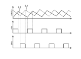
図4は、第1実施形態のスイッチング電源Xにおいて、電流バランスが改善する様子を示す図である。特に、本図では、先出の図3と同じく、上から順に、インダクタ電流IL1(破線)及びIL2(実線)、スイッチ電圧Vst1、並びに、スイッチ電圧Vst2が描写されている。
先述の通り、半導体装置X1及びX2は、互いに共通誤差信号Vc及び共通クロック信号CLK(例えば半導体装置X1で内部生成される誤差信号Vc1及びクロック信号CLK1)を共有している。
従って、半導体装置X1及びX2では、それぞれ、共通誤差信号Vc及び共通クロック信号CLKに応じてスイッチ電圧Vst1及びVst2それぞれのデューティ比が一致するように出力帰還制御が行われる。その結果、インダクタ電流IL1及びIL2の電流バランスが整えられるので、スイッチング電源Xの効率が向上する。
<更なる効率向上についての考察>
スイッチング電源Xの電流バランスを更に改善する手法としては、いわゆるアクティブ補正とパッシブ補正が挙げられる。
スイッチング電源Xの電流バランスを更に改善する手法としては、いわゆるアクティブ補正とパッシブ補正が挙げられる。
アクティブ補正では、半導体装置X1及びX2の相互間でインダクタ電流IL1及びIL2それぞれの電流情報が共有されることにより、電流バランスが高められる。ただし、本手法では、追加ピン及び高精度の電流検出回路が必要となるので、回路規模が大きくなり易い。また、本手法では、スイッチ出力段を形成するパワートランジスタのオン抵抗ばらつきを補正することが難しい。
パッシブ補正では、共通誤差信号Vc及び共通クロック信号CLKに応じてスイッチ電圧Vst1及びVst2それぞれのデューティ比を決定する帰還制御回路が高精度化されることにより、電流バランスが高められる。ただし、本手法では、高精度のトリミング回路が必要となる。また、本手法では、インダクタL1及びL2のDCR[direct current resistance]ばらつき、及び、スイッチ出力段を形成するパワートランジスタのオン抵抗ばらつきを補正することが難しい。
特に、半導体装置X1及びX2は、各個に独立した別のデバイスである。そのため、相互間の熱平衡も重要となり得る。
以下では、上記の考察に鑑み、スイッチング電源Xの電流バランスを更に改善することのできる新規な実施形態を提案する。
<スイッチング電源(第2実施形態)>
図5は、スイッチング電源の第2実施形態を示す図である。本実施形態のスイッチング電源Xは、先出の第1実施形態(図3)を基本としつつ、半導体装置X1の内部構成例がより具体的に描写されている。
図5は、スイッチング電源の第2実施形態を示す図である。本実施形態のスイッチング電源Xは、先出の第1実施形態(図3)を基本としつつ、半導体装置X1の内部構成例がより具体的に描写されている。
本図に即して述べると、半導体装置X1は、出力トランジスタM1と、同期整流トランジスタM2と、帰還制御回路100と、温度特性付与回路200と、を備える。
出力トランジスタM1は、ハーフブリッジの上側スイッチに相当する。出力トランジスタM1は、NMOSFET[N-channel type metal oxide semiconductor field effect transistor]であってもよい。出力トランジスタM1のドレインは、入力電圧Viの印加端に接続されている。出力トランジスタM1のソースは、スイッチ電圧Vst1の印加端に接続されている。出力トランジスタM1のゲートは、上側ゲート信号HGの印加端に接続されている。出力トランジスタM1は、上側ゲート信号HGがハイレベルであるときにオン状態となり、上側ゲート信号HGがローレベルであるときにオフ状態となる。
同期整流トランジスタM2は、ハーフブリッジの下側スイッチに相当する。同期整流トランジスタM2は、NMOSFETであってもよい。同期整流トランジスタM2のソースは、接地電圧GNDの印加端(=接地端)に接続されている。同期整流トランジスタM2のドレインは、スイッチ電圧Vst1の印加端に接続されている。同期整流トランジスタM2のゲートは、下側ゲート信号LGの印加端に接続されている。同期整流トランジスタM2は、下側ゲート信号LGがハイレベルであるときにオン状態となり、下側ゲート信号LGがローレベルであるときにオフ状態となる。
出力トランジスタM1と同期整流トランジスタM2は、上側ゲート信号HGと下側ゲート信号LGに応じて相補的にオン/オフされる。このようなオン/オフ動作により、インダクタL1の第1端には、入力電圧Viと接地電圧GNDとの間でパルス駆動される矩形波状のスイッチ電圧Vst1が生成される。上記の「相補的」という文言は、出力トランジスタM1と同期整流トランジスタM2のオン/オフ状態が完全に逆転している場合のほか、両トランジスタの同時オフ期間(デッドタイム)が設けられている場合も含む。
このように接続された出力トランジスタM1及び同期整流トランジスタM2は、先出のインダクタL1及びキャパシタC1と共に、入力電圧Viから出力電圧Voを生成するスイッチ出力段SW1を形成する。
なお、スイッチ出力段SW1の整流方式は、上記の同期整流方式に限らず、下側スイッチとして整流ダイオードを用いたダイオード整流方式であってもよい。また、出力トランジスタM1は、PMOSFETに置換されてもよい。また、出力トランジスタM1及び同期整流トランジスタM2は、半導体装置X1に外付けされてもよい。
特に、入力電圧Viとして高電圧が印加される場合には、出力トランジスタM1及び同期整流トランジスタM2として、それぞれ、パワーMOSFET、IGBT[insulated gate bipolar transistor]、及び、SiCトランジスタなどの高耐圧素子が用いられるとよい。また、出力トランジスタM1及び同期整流トランジスタM2として、それぞれ、GaNデバイスが用いられてもよい。
帰還制御回路100は、出力電圧Voに応じた帰還電圧Vfbと所定の基準電圧Vrefとの誤差信号Vc1に応じて、スイッチ出力段SW1のデューティ比Don1を決定する。なお、デューティ比Don1は、スイッチング周期Tsw1に占める出力トランジスタM1のオン期間Ton1の比率(=Ton1/Tsw1)として定義される。
本図に即して述べると、帰還制御回路100は、エラーアンプ101と、オシレータ102と、ランプ信号生成回路103と、電流検出回路104と、信号加算回路105と、コンパレータ106と、コントローラ107と、ドライバ108と、を含む。
エラーアンプ101は、反転入力端(-)に印加される帰還電圧Vfbと、非反転入力端(+)に印加される基準電圧Vrefとの差分に応じて、誤差信号Vc1(=電圧帰還情報)を生成する。誤差信号Vc1は、帰還電圧Vfbが基準電圧Vrefよりも低いときに上昇し、帰還電圧Vfbが基準電圧Vrefよりも高いときに低下する。
帰還電圧Vfbは、例えば、出力電圧Voの分圧電圧であってもよい。出力電圧Voがエラーアンプ101の入力ダイナミックレンジ内に収まっている場合には、出力電圧Voを帰還電圧Vfbとしてエラーアンプ101に直接入力しても構わない。また、基準電圧Vrefは、例えば、温度特性が比較的フラットなバンドギャップ電圧であってもよい。
オシレータ102は、所定のスイッチング周波数fsw1(=1/Tsw1)でパルス駆動されるクロック信号CLK1(=オン信号に相当)を生成する。
ランプ信号生成回路103は、出力トランジスタM1のオン期間Ton1に上昇する三角波状、鋸波状、又は、n次スロープ波状(例えばn=2)のランプ信号Vr1を生成する。ランプ信号Vr1は、例えば、出力トランジスタM1のオンタイミングでゼロ値から上昇を開始し、出力トランジスタM1のオフタイミングでゼロ値にリセットされる。
電流検出回路104は、例えば、出力トランジスタM1のオン期間Ton1において、スイッチ出力段SW1に流れるインダクタ電流IL1(以下では上側インダクタ電流IL1Hと呼ぶ)を検出して電流検出信号Vcs1(=電流帰還情報に相当)を生成する。
なお、上側インダクタ電流IL1Hの検出手法は任意である。例えば、出力トランジスタM1のドレイン・ソース間電圧を検出してもよいし、出力トランジスタM1に直列接続されたセンス抵抗の両端間電圧を検出してもよい。或いは、出力トランジスタM1に並列接続された電流検出用トランジスタのドレイン・ソース間電圧を検出してもよい。
信号加算回路105は、ランプ信号Vr1と電流検出信号Vcs1とを足し合わせてスロープ信号SLP1を生成する。
コンパレータ106は、反転入力端(-)に入力される誤差信号Vc1、より正確には誤差信号Vc1にダイオード201の順方向降下電圧Vf1が足し合わされたオフセット済みの誤差信号(Vc1+Vf1)と、非反転入力端(+)に入力されるスロープ信号SLP1とを比較することにより、比較信号CMP1(=オフ信号に相当)を生成する。このような比較処理により、出力トランジスタM1のオフタイミングが決定される。
比較信号CMP1は、SLP1<Vc1+Vf1であるときにハイレベルとなり、SLP1>Vc1+Vf1であるときにローレベルとなる。すなわち、比較信号CMP1のパルス生成タイミングは、オフセット済みの誤差信号(Vc1+Vf1)が高いほど遅くなり、オフセット済みの誤差信号(Vc1+Vf1)が低いほど早くなる。
コントローラ107は、クロック信号CLK1と比較信号CMP1に応じてパルス幅変調信号PWMを生成する。例えば、コントローラ107は、クロック信号CLK1にパルスが生成されたときにパルス幅変調信号PWMをハイレベル(=スイッチ電圧Vst1をハイレベルとするときの論理レベル)に立ち上げる。一方、コントローラ107は、比較信号CMP1にパルスが生成されたときにパルス幅変調信号PWMをローレベル(=スイッチ電圧Vst1をローレベルとするときの論理レベル)に立ち下げる。
従って、出力トランジスタM1のオン期間Ton1(=スイッチ電圧Vst1のハイレベル期間)は、比較信号CMP1のパルス生成タイミングが遅いほど長くなり、逆に、比較信号CMP1のパルス生成タイミングが早いほど短くなる。すなわち、スイッチ出力段SW1のデューティ比Don1(=Ton1/Tsw1)は、オフセット済みの誤差信号(Vc1+Vf1)が高いほど大きくなり、逆に、オフセット済みの誤差信号(Vc1+Vf1)が低いほど小さくなる。このように、コントローラ107は、クロック信号CLK1と比較信号CMP1に応じてデューティ比Don1を決定する。
ドライバ108は、パルス幅変調信号PWMに応じて上側ゲート信号HG及び下側ゲート信号LGを生成する。例えば、ドライバ108は、パルス幅変調信号PWMがハイレベルであるときに上側ゲート信号HGをハイレベルとして下側ゲート信号LGをローレベルとする。一方、ドライバ108は、パルス幅変調信号PWMがローレベルであるときに上側ゲート信号HGをローレベルとして下側ゲート信号LGをハイレベルとする。
また、半導体装置X1は、温度特性付与回路200を備える。温度特性付与回路200は、誤差信号Vc1からデューティ比Don1への変換係数に負の温度特性を持たせる。すなわち、誤差信号Vc1を固定値として仮定した場合、デューティ比Don1は、半導体装置X1の温度が高いほど小さくなり、半導体装置X1の温度が低いほど大きくなる。半導体装置X1の温度は、例えば、出力トランジスタM1の素子形成領域におけるジャンクション温度であってもよい。
本図に即して述べると、温度特性付与回路200は、ダイオード201を含む。ダイオード201のカソードは、エラーアンプ101の出力端(=誤差信号Vc1の印加端)に接続されている。一方、ダイオード201のアノードは、コンパレータ106の反転入力端(-)に接続されている。従って、コンパレータ106の反転入力端(-)には、誤差信号Vc1にダイオード201の順方向降下電圧Vf1を足し合わせた電圧信号(=オフセット済みの誤差信号(Vc1+Vf1)に相当)が印加される。
なお、ダイオード201の順方向降下電圧Vf1は、負の温度特性を持つ。すなわち、順方向降下電圧Vf1は、半導体装置X1の温度が高いほど低下し、半導体装置X1の温度が低いほど上昇する。従って、誤差信号Vc1を固定値として仮定した場合、オフセット済みの誤差信号(Vc1+Vf1)は、半導体装置X1の温度が高いほど低下し、半導体装置X1の温度が低いほど上昇する。
その結果、オフセット済みの誤差信号(Vc1+Vf1)とスロープ信号SLP1との交差タイミングは、半導体装置X1の温度が高いほど早くなり、半導体装置X1の温度が低いほど遅くなる。上記の交差タイミングは、出力トランジスタM1のオフタイミングに相当する。従って、スイッチ出力段SW1のデューティ比Don1は、半導体装置X1の温度が高いほど小さくなり、半導体装置X1の温度が低いほど大きくなる。
なお、半導体装置X1の温度は、一般に、スイッチ出力段SW1に流れるインダクタ電流IL1が大きいほど高くなり、インダクタ電流IL1が小さいほど低くなる。従って、インダクタ電流IL1が増大して半導体装置X1の温度が上昇すると、先に説明した温度特性付与回路200の働きによりデューティ比Don1が引き下げられる。逆に、インダクタ電流IL1が減少して半導体装置X1の温度が低下すると、温度特性付与回路200の働きによりデューティ比Don1が引き上げられる。その結果、インダクタ電流IL1は、所定の平衡状態に収束していく。
一方、スイッチ出力段SW2の駆動制御を行う半導体装置X2は、半導体装置X1と同一の機種であり、それぞれの内部構成は共通である。そのため、重複した説明は省略される。なお、本図では、半導体装置X1がマスタであって、半導体装置X2がスレーブである例が描写されている。この場合、半導体装置X1は、誤差信号Vc1及びクロック信号CLK1を先出の共通誤差信号Vc及び共通クロック信号CLKとして半導体装置X2に出力する。このとき、半導体装置X2のエラーアンプ及びオシレータ(いずれも不図示)は、いずれも無効状態(非動作状態)とされる。
ところで、インダクタ電流IL1及びIL2の電流バランスが崩れた場合には、半導体装置X1及びX2それぞれの温度にも差異が生じ得る。このように、半導体装置X1及びX2の温度が異なる場合、半導体装置X1で内部生成される誤差信号Vc1からデューティ比Don1への変換係数と、半導体装置X2の帰還制御に用いられる共通誤差信号Vc(=誤差信号Vc1)からデューティ比Don2への変換係数は、半導体装置X1及び2それぞれに導入される温度特性付与回路200の働きにより、意図的に異なる値となる。
その結果、半導体装置X1及びX2の温度が一致するように、延いては、インダクタ電流IL1及びIL2が一致するように、スイッチ出力段SW1及びSW2それぞれのデューティ比Don1及びDon2が増減される。以下では、このようなバランス制御のことを「熱平衡電流バランス制御」と呼ぶ。
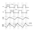
図6は、温度特性付与回路200の導入より実現される熱平衡電流バランス制御の一例を示す図である。本図では、上から順に、スイッチ電圧Vst1及びVst2、インダクタ電流IL1(実線)及びIL2(破線)、並びに、スロープ信号SLP1(実線)及びSLP2(破線)が描写されている。また、半導体装置X1及びX2それぞれに設けられるダイオード201の順方向降下電圧は、Vf1及びVf2として区別されている。
本図で示されているように、インダクタ電流IL2(破線)の方がインダクタ電流IL1(実線)よりも平均的に大きい場合を考える。この場合には、一般に、半導体装置X2の方が半導体装置X1よりも高温になる。そのため、順方向降下電圧Vf2の方が順方向降下電圧Vf1よりも低くなる。
一方、半導体装置X1及びX2では、いずれも共通誤差信号Vc(=Vc1)を用いて帰還性制御が行われる。従って、順方向降下電圧Vf2の方が順方向降下電圧Vf1よりも低い状況では、オフセット済みの誤差信号(Vc+Vf2)の方がオフセット済みの誤差信号(Vc+Vf1)よりも低くなる。
その結果、スイッチ電圧Vst2のデューティ比Don2(=Ton2/Tsw)が小さくなる方向、すなわち、インダクタ電流IL2が減少する方向に自然と制御が掛かる。従って、インダクタ電流IL1及びIL2の電流バランスが改善される方向に働く。
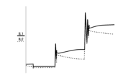
図7及び図8は、いずれも出力電流Ioの段階的な引き上げ(小→中→大)に伴うインダクタ電流IL1(実線)及びIL2(破線)それぞれの挙動を示す図である。各図の挙動は、互いの特性が意図的にずらされた半導体装置X1及びX2を用いてスタック方式のスイッチング電源1を構成した場合のシミュレーション結果である。なお、図7では、先述の熱平衡電流バランス制御が導入されていない場合の挙動が示されている。一方、図8では、先述の熱平衡電流バランス制御が導入されている場合の挙動が示されている。
両図を対比すれば明らかなように、熱平衡電流バランス制御の導入により、インダクタ電流IL1及びIL2の電流バランスが改善される。
<スイッチング電源(第3実施形態)>
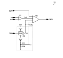
図9は、スイッチング電源の第3実施形態を示す図である。本実施形態のスイッチング電源Xは、先出の第2実施形態(図5)を基本としつつ、温度特性付与回路200の回路構成に変更が加えられている。また、この変更に伴い、コンパレータ106は、2入力型から4入力型に変更されている。
図9は、スイッチング電源の第3実施形態を示す図である。本実施形態のスイッチング電源Xは、先出の第2実施形態(図5)を基本としつつ、温度特性付与回路200の回路構成に変更が加えられている。また、この変更に伴い、コンパレータ106は、2入力型から4入力型に変更されている。
本図に即して述べると、温度特性付与回路200は、先出のダイオード201に代えてデジタル/アナログ変換回路202と、抵抗203及び204(抵抗値:R203及びR204)と、を含む。
デジタル/アナログ変換回路202は、デジタルのトリミング信号TRIMをアナログの第1電圧信号V1に変換する。第1電圧信号V1は、基準電圧Vrefと接地電圧GNDとの間の中間電圧であってもよい。なお、基準電圧Vrefの温度特性がフラットである場合、第1電圧信号V1の温度特性もフラットとなる。
抵抗203及び204は、基準電圧Vrefの印加端と接地電圧GNDの印加端との間に直列接続されており、相互間の接続ノードから第2電圧信号V2を出力する抵抗ラダーである。従って、第2電圧信号V2は、基準電圧Vrefの分圧電圧(=Vref×{R204/(R203+R204)})となる。
なお、抵抗203及び204としては、温度特性の異なる複数種類の抵抗が組み合わされるとよい。例えば、抵抗203の抵抗値R203は、正の温度特性を持ってもよい。また、抵抗204の抵抗値R204は、負の温度特性を持ってもよい。この場合、第2電圧信号V2が負の温度特性を持つ。具体的な例を挙げると、正の温度特性を持つ抵抗としては、インプラ抵抗(拡散抵抗)が用いられてもよい。また、負の温度特性を持つ抵抗としては、ポリ抵抗が用いられてもよい。
4入力型のコンパレータ106は、非反転入力端(+)同士の第1加算信号(SLP1+V1)と、反転入力端(-)同士の第2加算信号(Vc1+V2)とを比較することにより、比較信号CMP1を生成する。この場合、比較信号CMP1は、第1加算信号(SLP1+V1)が第2加算信号(Vc1+V2)よりも高いときにハイレベルとなる。また、比較信号CMP1は、第1加算信号(SLP1+V1)が第2加算信号(Vc1+V2)よりも低いときにローレベルとなる。上記の比較処理は、スロープ信号SLP1とオフセット済みの誤差信号(Vc1+Vofs)とを比較していることに他ならない(ただしVofs=V2-V1)。
このように、温度特性付与回路200は、温度特性の異なる複数種類の抵抗203及び204が組み合わされた抵抗ラダーを用いてコンパレータ106の入力オフセット電圧Vofs(=V2-V1)を設定する。
特に、第1電圧信号V1の温度特性がフラットであり、第2電圧信号V2が負の温度特性を持つ場合を考える。この場合、入力オフセット電圧Vofs(=V2-V1)は、負の温度特性を持つ。すなわち、温度特性付与回路200は、負の温度特性を持つ入力オフセット電圧Vofsをコンパレータ106に付与する。本構成であれば、先述と同様の熱平衡電流バランス制御が実現され得る。
なお、上記とは逆に、入力オフセット電圧Vofs(延いては第2電圧信号V2)は、正の温度特性を持ってもよい。この場合、第1電圧信号V1がコンパレータ106の反転入力端(-)に入力され、第2電圧信号V2がコンパレータ106の非反転入力端(+)に入力されればよい。
<スイッチング電源(第4実施形態)>
図10は、スイッチング電源の第4実施形態を示す図である。本実施形態のスイッチング電源Xは、先出の第3実施形態(図9)を基本としつつ、温度特性付与回路200の回路構成に変更が加えられている。
図10は、スイッチング電源の第4実施形態を示す図である。本実施形態のスイッチング電源Xは、先出の第3実施形態(図9)を基本としつつ、温度特性付与回路200の回路構成に変更が加えられている。
本図に即して述べると、温度特性付与回路200は、先出の構成要素202~204に代えて、PTAT[proportional to absolute temperature]電圧源205を含む。PTAT電圧源205は、絶対温度に比例したPTAT電圧を出力する。温度特性付与回路200は、このPTAT電圧源205を用いて入力オフセット電圧Vofsを設定する。なお、PTAT電圧源205の回路構成については、周知技術を適用すれば足りる。
本構成によれば、先出の第3実施形態(図9)と同様の作用・効果が享受され得る。
<スイッチング電源(第4実施形態)>
図11は、スイッチング電源の第5実施形態を示す図である。本実施形態のスイッチング電源Xは、先出の第2実施形態(図5)を基本としつつ、温度特性付与回路200の回路構成に変更が加えられている。また、本図では、ランプ信号生成回路103の回路構成が明示されている。
図11は、スイッチング電源の第5実施形態を示す図である。本実施形態のスイッチング電源Xは、先出の第2実施形態(図5)を基本としつつ、温度特性付与回路200の回路構成に変更が加えられている。また、本図では、ランプ信号生成回路103の回路構成が明示されている。
本図に即して述べると、温度特性付与回路200は、先出のダイオード201に代えて抵抗206(抵抗値:R206)を含む。また、ランプ信号生成回路103は、電流源103aと、キャパシタ103bと、スイッチ103cと、を含む。
電流源103aの第1端は、電源端に接続されている。電流源103aの第2端と抵抗206及びスイッチ103cそれぞれの第1端は、ランプ信号Vr1の印加端に接続されている。抵抗206の第2端は、キャパシタ103bの第1端に接続されている。キャパシタ103b及びスイッチ103cそれぞれの第2端は、接地端に接続されている。
電流源103aは、所定の基準電流Irefを生成する。キャパシタ103bは、スイッチ103cがオフ状態であるときに基準電流Irefにより充電される。スイッチ103cは、例えば、先出のパルス幅変調信号PWMに応じてオン/オフされる。
具体的に述べると、スイッチ103cは、パルス幅変調信号PWMがハイレベルであるときにオフ状態となる。このとき、キャパシタ103bが基準電流Irefにより充電されるので、ランプ信号Vr1が上昇する。一方、スイッチ103cは、パルス幅変調信号PWMがローレベルであるときにオン状態となる。このとき、キャパシタ103bが放電されるので、ランプ信号Vr1がゼロ値にリセットされる。
なお、ランプ信号Vr1は、キャパシタ103bの充電電圧に抵抗206の両端間電圧(=Iref×R206)が足し合わされた電圧信号である。特に、抵抗206の抵抗値R206は、正の温度特性を持つとよい。本構成であれば、ランプ信号Vr1(延いてはスロープ信号SLP1)に正の温度特性を持つオフセットが付与される。このような構成は、誤差信号Vc1に負の温度特性を持つオフセットが付与される構成と等価である。
従って、本実施形態であれば、先出の第2実施形態(図5)、第3実施形態(図9)及び第4実施形態(図10)と同様の作用・効果が享受され得る。
<付記>
以下では、上記で説明した種々の実施形態について総括的に述べる。
以下では、上記で説明した種々の実施形態について総括的に述べる。
例えば、本明細書中に開示されている電源制御装置は、入力電圧から出力電圧を生成するスイッチ出力段の駆動制御を行うように構成された電源制御装置であって、前記出力電圧に応じた帰還電圧と所定の基準電圧との誤差信号に応じて前記スイッチ出力段のデューティ比を決定するように構成された帰還制御回路と、前記誤差信号から前記デューティ比への変換係数に負の温度特性を持たせるように構成された温度特性付与回路と、を備える構成(第1の構成)とされている。
上記第1の構成による電源制御装置において、前記帰還制御回路は、前記帰還電圧と前記基準電圧との差分に応じて前記誤差信号を生成するように構成されたエラーアンプと、前記誤差信号とスロープ信号とを比較して比較信号を生成するように構成されたコンパレータと、クロック信号及び前記比較信号に応じて前記デューティ比を決定するように構成されたコントローラと、を含む構成(第2の構成)としてもよい。
上記第2の構成による電源制御装置において、前記温度特性付与回路は、順方向降下電圧が負の温度特性を持つダイオードを含み、前記順方向降下電圧が前記誤差信号に足し合わされる構成(第3の構成)としてもよい。
上記第2の構成による電源制御装置において、前記温度特性付与回路は、負又は正の温度特性を持つ入力オフセット電圧を前記コンパレータに付与する構成(第4の構成)としてもよい。
上記第4の構成による電源制御装置において、前記温度特性付与回路は、温度特性の異なる複数種類の抵抗が組み合わされた抵抗ラダーを用いて前記入力オフセット電圧を設定する構成(第5の構成)としてもよい。
上記第4の構成による電源制御装置において、前記温度特性付与回路は、PTAT電圧源を用いて前記入力オフセット電圧を設定する構成(第6の構成)としてもよい。
上記第2の構成による電源制御装置において、前記温度特性付与回路は、抵抗値が正の温度特性を持つ抵抗を含み、前記抵抗の両端間電圧が前記スロープ信号に足し合わされる構成(第7の構成)としてもよい。
上記第2~第7いずれかの構成による電源制御装置において、前記帰還制御回路は、ランプ信号を生成するように構成されたランプ信号生成回路と、前記スイッチ出力段に流れるインダクタ電流に応じた電流検出信号を生成するように構成された電流検出回路と、前記ランプ信号と前記電流検出信号とを足し合わせて前記スロープ信号を生成するように構成された信号加算回路と、をさらに含む構成(第8の構成)としてもよい。
また、例えば、本明細書中に開示されているスイッチング電源は、出力が共通化された複数のスイッチ出力段と、前記複数のスイッチ出力段それぞれの駆動制御を行うように構成された複数の電源制御装置と、を備え、前記複数の電源制御装置は、それぞれ、上記第1~第8いずれかの構成による電源制御装置である構成(第9の構成)とされている。
なお、上記第9の構成によるスイッチング電源において、前記複数の電源制御装置は、いずれか一つがマスタであってその余がスレーブであり、前記マスタは、前記誤差信号を自ら内部生成し、前記誤差信号に応じて前記デューティ比を決定するとともに、前記誤差信号を共通誤差信号として前記スレーブに出力し、前記スレーブは、前記マスタから出力される前記共通誤差信号に応じて前記デューティ比を決定する構成(第10の構成)としてもよい。
<その他>
なお、本明細書中に開示されている種々の技術的特徴は、上記実施形態のほか、その技術的創作の主旨を逸脱しない範囲で種々の変更を加えることが可能である。すなわち、上記実施形態は、全ての点で例示であって制限的なものではないと考えられるべきである。また、本開示の技術的範囲は、特許請求の範囲により規定されるものであって、特許請求の範囲と均等の意味及び範囲内に属する全ての変更が含まれると理解されるべきである。
なお、本明細書中に開示されている種々の技術的特徴は、上記実施形態のほか、その技術的創作の主旨を逸脱しない範囲で種々の変更を加えることが可能である。すなわち、上記実施形態は、全ての点で例示であって制限的なものではないと考えられるべきである。また、本開示の技術的範囲は、特許請求の範囲により規定されるものであって、特許請求の範囲と均等の意味及び範囲内に属する全ての変更が含まれると理解されるべきである。
100 帰還制御回路
101 エラーアンプ
102 オシレータ
103 ランプ信号生成回路
103a 電流源
103b キャパシタ
103c スイッチ
104 電流検出回路
105 信号加算回路
106 コンパレータ
107 コントローラ
108 ドライバ
200 温度特性付与回路
201 ダイオード
202 デジタル/アナログ変換回路
203、204 抵抗
205 PTAT電圧源
206 抵抗
C1、C2 キャパシタ
L1、L2 インダクタ
M1 出力トランジスタ
M2 同期整流トランジスタ
X、Y スイッチング電源
X1、X2、Y1、Y2 半導体装置(電源制御装置)
Z 負荷
101 エラーアンプ
102 オシレータ
103 ランプ信号生成回路
103a 電流源
103b キャパシタ
103c スイッチ
104 電流検出回路
105 信号加算回路
106 コンパレータ
107 コントローラ
108 ドライバ
200 温度特性付与回路
201 ダイオード
202 デジタル/アナログ変換回路
203、204 抵抗
205 PTAT電圧源
206 抵抗
C1、C2 キャパシタ
L1、L2 インダクタ
M1 出力トランジスタ
M2 同期整流トランジスタ
X、Y スイッチング電源
X1、X2、Y1、Y2 半導体装置(電源制御装置)
Z 負荷
Claims (10)
- 入力電圧から出力電圧を生成するスイッチ出力段の駆動制御を行うように構成された電源制御装置であって、
前記出力電圧に応じた帰還電圧と所定の基準電圧との誤差信号に応じて前記スイッチ出力段のデューティ比を決定するように構成された帰還制御回路と、
前記誤差信号から前記デューティ比への変換係数に負の温度特性を持たせるように構成された温度特性付与回路と、
を備える、電源制御装置。 - 前記帰還制御回路は、
前記帰還電圧と前記基準電圧との差分に応じて前記誤差信号を生成するように構成されたエラーアンプと、
前記誤差信号とスロープ信号とを比較して比較信号を生成するように構成されたコンパレータと、
クロック信号及び前記比較信号に応じて前記デューティ比を決定するように構成されたコントローラと、
を含む、請求項1に記載の電源制御装置。 - 前記温度特性付与回路は、順方向降下電圧が負の温度特性を持つダイオードを含み、前記順方向降下電圧が前記誤差信号に足し合わされる、請求項2に記載の電源制御装置。
- 前記温度特性付与回路は、負又は正の温度特性を持つ入力オフセット電圧を前記コンパレータに付与する、請求項2に記載の電源制御装置。
- 前記温度特性付与回路は、温度特性の異なる複数種類の抵抗が組み合わされた抵抗ラダーを用いて前記入力オフセット電圧を設定する、請求項4に記載の電源制御装置。
- 前記温度特性付与回路は、PTAT電圧源を用いて前記入力オフセット電圧を設定する、請求項4に記載の電源制御装置。
- 前記温度特性付与回路は、抵抗値が正の温度特性を持つ抵抗を含み、前記抵抗の両端間電圧が前記スロープ信号に足し合わされる、請求項2に記載の電源制御装置。
- 前記帰還制御回路は、
ランプ信号を生成するように構成されたランプ信号生成回路と、
前記スイッチ出力段に流れるインダクタ電流に応じた電流検出信号を生成するように構成された電流検出回路と、
前記ランプ信号と前記電流検出信号とを足し合わせて前記スロープ信号を生成するように構成された信号加算回路と、
をさらに含む、請求項2~7のいずれか一項に記載の電源制御装置。 - 出力が共通化された複数のスイッチ出力段と、
前記複数のスイッチ出力段それぞれの駆動制御を行うように構成された複数の電源制御装置と、
を備え、
前記複数の電源制御装置は、それぞれ、請求項1~8のいずれか一項に記載の電源制御装置である、スイッチング電源。 - 前記複数の電源制御装置は、いずれか一つがマスタであってその余がスレーブであり、
前記マスタは、前記誤差信号を自ら内部生成し、前記誤差信号に応じて前記デューティ比を決定するとともに、前記誤差信号を共通誤差信号として前記スレーブに出力し、
前記スレーブは、前記マスタから出力される前記共通誤差信号に応じて前記デューティ比を決定する、請求項9に記載のスイッチング電源。
Applications Claiming Priority (2)
| Application Number | Priority Date | Filing Date | Title |
|---|---|---|---|
| JP2023-007375 | 2023-01-20 | ||
| JP2023007375 | 2023-01-20 |
Publications (1)
| Publication Number | Publication Date |
|---|---|
| WO2024154487A1 true WO2024154487A1 (ja) | 2024-07-25 |
Family
ID=91955733
Family Applications (1)
| Application Number | Title | Priority Date | Filing Date |
|---|---|---|---|
| PCT/JP2023/044594 Ceased WO2024154487A1 (ja) | 2023-01-20 | 2023-12-13 | 電源制御装置、スイッチング電源 |
Country Status (1)
| Country | Link |
|---|---|
| WO (1) | WO2024154487A1 (ja) |
Citations (5)
| Publication number | Priority date | Publication date | Assignee | Title |
|---|---|---|---|---|
| JP2009153278A (ja) * | 2007-12-19 | 2009-07-09 | Sharp Corp | スイッチング電源回路 |
| US20120299560A1 (en) * | 2011-05-25 | 2012-11-29 | Linear Technology Corporation | Balancing Temperatures in A Multi-Phase DC/DC Converter |
| JP2014075932A (ja) * | 2012-10-05 | 2014-04-24 | Rohm Co Ltd | 電源装置及びこれを用いた電子機器 |
| JP2020156224A (ja) * | 2019-03-20 | 2020-09-24 | 横河電機株式会社 | 電源システム及び電源装置 |
| US10795390B1 (en) * | 2020-01-28 | 2020-10-06 | Alpha And Omega Semiconductor (Cayman) Ltd. | DC resistance sense temperature compensation |
-
2023
- 2023-12-13 WO PCT/JP2023/044594 patent/WO2024154487A1/ja not_active Ceased
Patent Citations (5)
| Publication number | Priority date | Publication date | Assignee | Title |
|---|---|---|---|---|
| JP2009153278A (ja) * | 2007-12-19 | 2009-07-09 | Sharp Corp | スイッチング電源回路 |
| US20120299560A1 (en) * | 2011-05-25 | 2012-11-29 | Linear Technology Corporation | Balancing Temperatures in A Multi-Phase DC/DC Converter |
| JP2014075932A (ja) * | 2012-10-05 | 2014-04-24 | Rohm Co Ltd | 電源装置及びこれを用いた電子機器 |
| JP2020156224A (ja) * | 2019-03-20 | 2020-09-24 | 横河電機株式会社 | 電源システム及び電源装置 |
| US10795390B1 (en) * | 2020-01-28 | 2020-10-06 | Alpha And Omega Semiconductor (Cayman) Ltd. | DC resistance sense temperature compensation |
Similar Documents
| Publication | Publication Date | Title |
|---|---|---|
| US10763748B2 (en) | Buck-boost DC-DC converter | |
| US8072195B2 (en) | Voltage converter | |
| US9035632B2 (en) | DC-DC converter, control circuit, and power supply control method | |
| CN103023317B (zh) | Dc/dc转换器 | |
| CN211046763U (zh) | 电子转换器和降压型开关转换器 | |
| JP5369555B2 (ja) | 電流モード制御型スイッチングレギュレータ及びその動作制御方法 | |
| JP2000092824A (ja) | スイッチングレギュレータおよびlsiシステム | |
| KR20170120605A (ko) | 유한 상태 기계 제어를 사용하는 다중-레벨 스위칭 조절기 회로들 및 방법들 | |
| JP2005168169A (ja) | 電源回路及びその電源回路の出力電圧変更方法 | |
| JP5470772B2 (ja) | 電流モード制御型スイッチングレギュレータ | |
| TW201444242A (zh) | 直流轉直流轉換控制器 | |
| CN102318174B (zh) | 不连续dc-dc电压转换器中的输出电流感测方法 | |
| CN102751864B (zh) | 基于Cuk的电流源 | |
| CN107112893A (zh) | 功率转换装置 | |
| US11777405B2 (en) | Boost off time adaptive adjustment unit and power converter comprising the same | |
| JP2010183335A (ja) | パルス幅変調回路、パルス幅変調方法及びレギュレータ | |
| JP6831713B2 (ja) | ブートストラップ回路 | |
| CN101449451B (zh) | 电荷泵控制器及其方法 | |
| US8476878B2 (en) | Startup circuit for DC-DC converter | |
| CN116488434A (zh) | 升降压转换器及其控制电路 | |
| US20070052398A1 (en) | DC-DC converter and its control method, and switching regulator and its control method | |
| JP2013215034A (ja) | Dc−dcコンバータ | |
| WO2024154487A1 (ja) | 電源制御装置、スイッチング電源 | |
| JP5604596B2 (ja) | Dc/dcコンバータ | |
| CN113972814A (zh) | 开关功率转换器的占空比控制 |
Legal Events
| Date | Code | Title | Description |
|---|---|---|---|
| 121 | Ep: the epo has been informed by wipo that ep was designated in this application |
Ref document number: 23917698 Country of ref document: EP Kind code of ref document: A1 |
|
| NENP | Non-entry into the national phase |
Ref country code: DE |
|
| 122 | Ep: pct application non-entry in european phase |
Ref document number: 23917698 Country of ref document: EP Kind code of ref document: A1 |