WO2024154358A1 - デバイスおよびデバイスの製造方法 - Google Patents
デバイスおよびデバイスの製造方法 Download PDFInfo
- Publication number
- WO2024154358A1 WO2024154358A1 PCT/JP2023/001780 JP2023001780W WO2024154358A1 WO 2024154358 A1 WO2024154358 A1 WO 2024154358A1 JP 2023001780 W JP2023001780 W JP 2023001780W WO 2024154358 A1 WO2024154358 A1 WO 2024154358A1
- Authority
- WO
- WIPO (PCT)
- Prior art keywords
- electrode
- substrate
- wiring
- hole
- insulating film
- Prior art date
- Legal status (The legal status is an assumption and is not a legal conclusion. Google has not performed a legal analysis and makes no representation as to the accuracy of the status listed.)
- Ceased
Links
Images









Classifications
-
- H—ELECTRICITY
- H10—SEMICONDUCTOR DEVICES; ELECTRIC SOLID-STATE DEVICES NOT OTHERWISE PROVIDED FOR
- H10W—GENERIC PACKAGES, INTERCONNECTIONS, CONNECTORS OR OTHER CONSTRUCTIONAL DETAILS OF DEVICES COVERED BY CLASS H10
- H10W70/00—Package substrates; Interposers; Redistribution layers [RDL]
- H10W70/60—Insulating or insulated package substrates; Interposers; Redistribution layers
- H10W70/62—Insulating or insulated package substrates; Interposers; Redistribution layers characterised by their interconnections
- H10W70/66—Conductive materials thereof
- H10W70/668—Superconducting materials
-
- H—ELECTRICITY
- H10—SEMICONDUCTOR DEVICES; ELECTRIC SOLID-STATE DEVICES NOT OTHERWISE PROVIDED FOR
- H10N—ELECTRIC SOLID-STATE DEVICES NOT OTHERWISE PROVIDED FOR
- H10N60/00—Superconducting devices
- H10N60/01—Manufacture or treatment
-
- H—ELECTRICITY
- H10—SEMICONDUCTOR DEVICES; ELECTRIC SOLID-STATE DEVICES NOT OTHERWISE PROVIDED FOR
- H10N—ELECTRIC SOLID-STATE DEVICES NOT OTHERWISE PROVIDED FOR
- H10N60/00—Superconducting devices
- H10N60/01—Manufacture or treatment
- H10N60/0241—Manufacture or treatment of devices comprising nitrides or carbonitrides
-
- H—ELECTRICITY
- H10—SEMICONDUCTOR DEVICES; ELECTRIC SOLID-STATE DEVICES NOT OTHERWISE PROVIDED FOR
- H10N—ELECTRIC SOLID-STATE DEVICES NOT OTHERWISE PROVIDED FOR
- H10N60/00—Superconducting devices
- H10N60/10—Junction-based devices
- H10N60/12—Josephson-effect devices
-
- H—ELECTRICITY
- H10—SEMICONDUCTOR DEVICES; ELECTRIC SOLID-STATE DEVICES NOT OTHERWISE PROVIDED FOR
- H10N—ELECTRIC SOLID-STATE DEVICES NOT OTHERWISE PROVIDED FOR
- H10N60/00—Superconducting devices
- H10N60/80—Constructional details
- H10N60/805—Constructional details for Josephson-effect devices
-
- H—ELECTRICITY
- H10—SEMICONDUCTOR DEVICES; ELECTRIC SOLID-STATE DEVICES NOT OTHERWISE PROVIDED FOR
- H10N—ELECTRIC SOLID-STATE DEVICES NOT OTHERWISE PROVIDED FOR
- H10N60/00—Superconducting devices
- H10N60/80—Constructional details
- H10N60/81—Containers; Mountings
- H10N60/815—Containers; Mountings for Josephson-effect devices
-
- H—ELECTRICITY
- H10—SEMICONDUCTOR DEVICES; ELECTRIC SOLID-STATE DEVICES NOT OTHERWISE PROVIDED FOR
- H10N—ELECTRIC SOLID-STATE DEVICES NOT OTHERWISE PROVIDED FOR
- H10N69/00—Integrated devices, or assemblies of multiple devices, comprising at least one superconducting element covered by group H10N60/00
-
- H—ELECTRICITY
- H10—SEMICONDUCTOR DEVICES; ELECTRIC SOLID-STATE DEVICES NOT OTHERWISE PROVIDED FOR
- H10P—GENERIC PROCESSES OR APPARATUS FOR THE MANUFACTURE OR TREATMENT OF DEVICES COVERED BY CLASS H10
- H10P14/00—Formation of materials, e.g. in the shape of layers or pillars
- H10P14/40—Formation of materials, e.g. in the shape of layers or pillars of conductive or resistive materials
-
- H—ELECTRICITY
- H10—SEMICONDUCTOR DEVICES; ELECTRIC SOLID-STATE DEVICES NOT OTHERWISE PROVIDED FOR
- H10W—GENERIC PACKAGES, INTERCONNECTIONS, CONNECTORS OR OTHER CONSTRUCTIONAL DETAILS OF DEVICES COVERED BY CLASS H10
- H10W20/00—Interconnections in chips, wafers or substrates
- H10W20/01—Manufacture or treatment
-
- H—ELECTRICITY
- H10—SEMICONDUCTOR DEVICES; ELECTRIC SOLID-STATE DEVICES NOT OTHERWISE PROVIDED FOR
- H10W—GENERIC PACKAGES, INTERCONNECTIONS, CONNECTORS OR OTHER CONSTRUCTIONAL DETAILS OF DEVICES COVERED BY CLASS H10
- H10W20/00—Interconnections in chips, wafers or substrates
- H10W20/40—Interconnections external to wafers or substrates, e.g. back-end-of-line [BEOL] metallisations or vias connecting to gate electrodes
-
- H—ELECTRICITY
- H10—SEMICONDUCTOR DEVICES; ELECTRIC SOLID-STATE DEVICES NOT OTHERWISE PROVIDED FOR
- H10W—GENERIC PACKAGES, INTERCONNECTIONS, CONNECTORS OR OTHER CONSTRUCTIONAL DETAILS OF DEVICES COVERED BY CLASS H10
- H10W70/00—Package substrates; Interposers; Redistribution layers [RDL]
- H10W70/01—Manufacture or treatment
- H10W70/05—Manufacture or treatment of insulating or insulated package substrates, or of interposers, or of redistribution layers
-
- H—ELECTRICITY
- H10—SEMICONDUCTOR DEVICES; ELECTRIC SOLID-STATE DEVICES NOT OTHERWISE PROVIDED FOR
- H10W—GENERIC PACKAGES, INTERCONNECTIONS, CONNECTORS OR OTHER CONSTRUCTIONAL DETAILS OF DEVICES COVERED BY CLASS H10
- H10W70/00—Package substrates; Interposers; Redistribution layers [RDL]
- H10W70/01—Manufacture or treatment
- H10W70/05—Manufacture or treatment of insulating or insulated package substrates, or of interposers, or of redistribution layers
- H10W70/095—Manufacture or treatment of insulating or insulated package substrates, or of interposers, or of redistribution layers of vias therein
-
- H—ELECTRICITY
- H10—SEMICONDUCTOR DEVICES; ELECTRIC SOLID-STATE DEVICES NOT OTHERWISE PROVIDED FOR
- H10W—GENERIC PACKAGES, INTERCONNECTIONS, CONNECTORS OR OTHER CONSTRUCTIONAL DETAILS OF DEVICES COVERED BY CLASS H10
- H10W70/00—Package substrates; Interposers; Redistribution layers [RDL]
- H10W70/60—Insulating or insulated package substrates; Interposers; Redistribution layers
- H10W70/611—Insulating or insulated package substrates; Interposers; Redistribution layers for connecting multiple chips together
-
- H—ELECTRICITY
- H10—SEMICONDUCTOR DEVICES; ELECTRIC SOLID-STATE DEVICES NOT OTHERWISE PROVIDED FOR
- H10W—GENERIC PACKAGES, INTERCONNECTIONS, CONNECTORS OR OTHER CONSTRUCTIONAL DETAILS OF DEVICES COVERED BY CLASS H10
- H10W70/00—Package substrates; Interposers; Redistribution layers [RDL]
- H10W70/60—Insulating or insulated package substrates; Interposers; Redistribution layers
- H10W70/62—Insulating or insulated package substrates; Interposers; Redistribution layers characterised by their interconnections
- H10W70/63—Vias, e.g. via plugs
- H10W70/635—Through-vias
-
- H—ELECTRICITY
- H10—SEMICONDUCTOR DEVICES; ELECTRIC SOLID-STATE DEVICES NOT OTHERWISE PROVIDED FOR
- H10W—GENERIC PACKAGES, INTERCONNECTIONS, CONNECTORS OR OTHER CONSTRUCTIONAL DETAILS OF DEVICES COVERED BY CLASS H10
- H10W70/00—Package substrates; Interposers; Redistribution layers [RDL]
- H10W70/60—Insulating or insulated package substrates; Interposers; Redistribution layers
- H10W70/67—Insulating or insulated package substrates; Interposers; Redistribution layers characterised by their insulating layers or insulating parts
- H10W70/68—Shapes or dispositions thereof
- H10W70/685—Shapes or dispositions thereof comprising multiple insulating layers
-
- H—ELECTRICITY
- H10—SEMICONDUCTOR DEVICES; ELECTRIC SOLID-STATE DEVICES NOT OTHERWISE PROVIDED FOR
- H10W—GENERIC PACKAGES, INTERCONNECTIONS, CONNECTORS OR OTHER CONSTRUCTIONAL DETAILS OF DEVICES COVERED BY CLASS H10
- H10W70/00—Package substrates; Interposers; Redistribution layers [RDL]
- H10W70/60—Insulating or insulated package substrates; Interposers; Redistribution layers
- H10W70/67—Insulating or insulated package substrates; Interposers; Redistribution layers characterised by their insulating layers or insulating parts
- H10W70/69—Insulating materials thereof
- H10W70/698—Semiconductor materials that are electrically insulating, e.g. undoped silicon
Definitions
- the present invention relates to a device and a method for manufacturing the device.
- Interposers are known, which are relay substrates that use through-hole electrodes to provide electrical continuity between circuits on the front and back sides. For example, it is known to flip-chip mount quantum bit chips on interposers (see, for example, Patent Documents 1 to 3). There is also a known configuration in which quantum bit elements and passive elements provided on the front and back sides of a substrate are connected by through-hole electrodes (see, for example, Patent Document 4).
- the through electrode When a through electrode is provided so as to fill a through hole penetrating a substrate, the difference in the linear expansion coefficient between the substrate and the through electrode may cause damage to the substrate and/or the through electrode. Therefore, in order to reduce the volume of the through electrode, the through electrode may be made cylindrical and conform to the inner wall surface of the through hole. However, in this case, the connection area between the wiring formed on the substrate and the through electrode becomes smaller, which may cause the contact between the wiring and the through electrode to become unstable.
- the aim is to increase the connection area between the through electrode and the wiring.
- the device includes a substrate having a first surface, a second surface opposite the first surface, and a through hole penetrating between the first surface and the second surface, a through electrode provided in the through hole and having a side portion along the inner wall surface of the through hole and a bottom portion connected to the side portion, a protective film provided on the through hole closer to the center than the through electrode, and a first wiring provided on the second surface of the substrate and connected to the bottom portion of the through electrode.
- the method for manufacturing a device includes the steps of forming a through hole that penetrates between a first surface of a substrate and a second surface opposite the first surface, forming a through electrode having a side portion along the inner wall surface of the through hole and a bottom portion connected to the side portion, forming a protective film on the through hole closer to the center than the through electrode, and forming a first wiring connected to the bottom portion of the through electrode on the second surface of the substrate.
- One aspect is that it is possible to increase the connection area between the through electrode and the wiring.
- FIG. 1 is a cross-sectional view of a device according to a first embodiment.
- FIG. 2A is a plan view of the through electrode in the first embodiment as viewed from the +Z direction
- FIG. 2B is a plan view as viewed from the -Z direction.
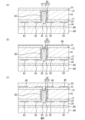
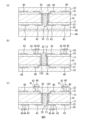
- 3A to 3C are cross-sectional views (part 1) illustrating a method for manufacturing a device according to the first embodiment.
- 4A to 4C are cross-sectional views (part 2) illustrating the method for manufacturing the device according to the first embodiment.
- 5A to 5C are cross-sectional views (part 3) illustrating the method for manufacturing the device according to the first embodiment.
- 6A to 6C are cross-sectional views (part 4) illustrating the method for manufacturing the device according to the first embodiment.
- FIG. 7A to 7C are cross-sectional views (part 5) illustrating the method for manufacturing the device according to the first embodiment.
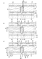
- 8A to 8C are cross-sectional views (part 1) showing a method for manufacturing a device according to Comparative Example 1.
- FIG. 9A to 9C are cross-sectional views (part 2) showing a method for manufacturing a device according to Comparative Example 1.
- FIG. 10A and 10B are cross-sectional views showing an example in which no cavity is formed in the through hole in the first embodiment.
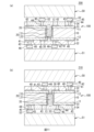
- FIG. 11A is a cross-sectional view of a device according to the second embodiment
- FIG. 11B is a cross-sectional view of a device according to a modified example of the second embodiment.
- FIG. 12 is a cross-sectional view of a device according to the third embodiment.
- FIG. 13(a) is a plan view of a quantum bit element in Example 3, and FIG. 13(b) is a cross-sectional view taken along line AA of FIG. 13(a).
- 14A to 14C are cross-sectional views (part 1) illustrating a method for manufacturing a device according to the third embodiment.
- 15A to 15C are cross-sectional views (part 2) illustrating a method for manufacturing a device according to the third embodiment.
- 16A to 16C are cross-sectional views (part 1) illustrating a method for manufacturing a quantum bit element and a third wiring pattern in the third embodiment.
- 17A to 17C are cross-sectional views (part 2) illustrating a method for manufacturing a quantum bit element and a third wiring pattern in the third embodiment.
- FIG. 1 is a plan view of a quantum bit element in Example 3
- FIG. 13(b) is a cross-sectional view taken along line AA of FIG. 13(a).
- 14A to 14C are cross-sectional views (part 1) illustrating
- FIG. 18 is a cross-sectional view of a device according to a modified example of the third embodiment.
- 19A to 19C are cross-sectional views showing a method for manufacturing a device according to a modified example of the third embodiment.
- 20A to 20C are cross-sectional views (part 1) showing a method for manufacturing a device according to Comparative Example 2.
- 21A to 21C are cross-sectional views (part 2) showing a method for manufacturing a device according to Comparative Example 2.
- FIG. FIG. 22(a) is a cross-sectional view of a device according to Example 4, and
- FIG. 22(b) is a cross-sectional view of a device according to a modified example of Example 4.
- FIG. 1 is a cross-sectional view of a device according to Example 1.
- Example 1 shows an example in which device 100 is an interposer. The directions parallel to and perpendicular to first surface 11 of substrate 10 are defined as X-axis and Y-axis, and the thickness direction of substrate 10 is defined as Z-axis.
- device 100 according to Example 1 has substrate 10 having first surface 11 and second surface 12 opposite to first surface 11, and through-hole 13 penetrating between first surface 11 and second surface 12.
- Substrate 10 is, for example, a silicon substrate, a glass substrate, or a quartz substrate.
- Through-hole 13 has, for example, a diameter of about 5 ⁇ m to 15 ⁇ m and a depth of about 100 ⁇ m to 300 ⁇ m.
- a through electrode 20 is provided in the through hole 13.
- the through electrode 20 has a cylindrical side portion 21 that extends along the inner wall surface of the through hole 13, and a bottom portion 22 that is a plate-shaped portion that is connected to the end of the side portion 21 and is provided overlapping the cylindrical interior of the side portion 21 in a planar view.
- An insulating film 30 is provided between the inner wall surface of the through hole 13 and the through electrode 20.
- the through electrode 20 is formed, for example, from titanium nitride, and has a thickness of, for example, about 50 nm to 150 nm.
- the insulating film 30 is formed, for example, from silicon oxide, and has a thickness of, for example, 50 nm to 150 nm.
- FIG. 2(a) is a plan view of the through electrode in Example 1 as viewed from the +Z direction
- FIG. 2(b) is a plan view as viewed from the -Z direction.
- the through electrode 20 is hatched to clarify the drawings.
- the side portion 21 of the through electrode 20 is cylindrically formed along the inner wall surface of the through hole 13.
- the bottom portion 22 is connected to the end of the side portion 21 and covers the cylindrical interior of the side portion 21.
- the through electrode 20 has a concave shape.
- one or more first wiring patterns 40 are provided on the second surface 12 of the substrate 10 via an insulating film 31.
- the first wiring patterns 40 that overlap the through holes 13 among the one or more first wiring patterns 40 enter the insulating film 31 and the openings provided in the insulating film 30 and connect to the bottom 22 of the through electrode 20.
- FIG. 2(a) and FIG. 2(b) the range in which the first wiring pattern 40 contacts the bottom 22 is illustrated by dotted lines.
- the first wiring pattern 40 contacts more than half of the surface of the bottom 22 on the first wiring pattern 40 side (the shaded area in FIG. 2(b)).
- the first wiring pattern 40 is formed of, for example, titanium nitride, and has a thickness of, for example, 50 nm to 150 nm.
- the insulating film 31 is formed of, for example, silicon oxide, and has a thickness of, for example, about 50 nm to 150 nm.
- An insulating film 32 is provided on the second surface 12 of the substrate 10, covering one or more first wiring patterns 40.
- a through-wire 41 is provided, which is embedded in an opening provided in the insulating film 32 and connected to the first wiring pattern 40.
- a first terminal electrode 42 is provided on the insulating film 32, which is connected to the through-wire 41 and serves as a terminal for external connection.
- a bump electrode 46 is provided on the surface of the first terminal electrode 42.
- the insulating film 32 is formed of, for example, silicon oxide, and has a thickness of, for example, 100 nm to 300 nm.
- the first terminal electrode 42 is formed of a high-melting point metal material, such as vanadium, molybdenum, hafnium, or tantalum.
- the through-wire 41 may be formed of the same material as the first terminal electrode 42, or may be formed of a different material.
- the bump electrode 46 is formed of, for example, indium, gallium, or solder.
- One or more second wiring patterns 43 are provided on the first surface 11 of the substrate 10 via an insulating film 33. At least a part of the one or more second wiring patterns 43 is provided extending from the side 21 of the through electrode 20.
- An insulating film 34 is provided on the first surface 11 of the substrate 10 to cover the one or more second wiring patterns 43. A part of the insulating film 34 enters the through hole 13 and covers the surface of the side 21 and the bottom 22 of the through electrode 20. A cavity 35 is formed inside the insulating film 34 of the through hole 13. By covering the through electrode 20 with the insulating film 34, the through electrode 20 is protected and unintended conduction is suppressed.
- a through wiring 44 is provided that is embedded in an opening provided in the insulating film 34 and connected to the second wiring pattern 43.
- a second terminal electrode 45 that is connected to the through wiring 44 and serves as a terminal for external connection is provided on the insulating film 34.
- the second wiring pattern 43 is formed, for example, from titanium nitride and has a thickness of, for example, 50 nm to 150 nm.
- the insulating film 33 is formed, for example, from silicon oxide and has a thickness of, for example, about 50 nm to 150 nm.
- the insulating film 34 is formed, for example, from silicon oxide and has a thickness of, for example, 100 nm to 300 nm.
- the second terminal electrode 45 is formed of a high-melting point metal material, like the first terminal electrode 42.
- the through wiring 44 may be formed of the same material as the second terminal electrode 45, or may be formed of a different material.
- the insulating film 34 provided closer to the center than the through electrode 20 of the through hole 13 is made of, for example, silicon oxide.
- the through electrode 20 is made of, for example, titanium nitride.
- the substrate 10 is made of, for example, silicon.
- the linear expansion coefficient of silicon oxide is 0.5 ⁇ 10 ⁇ 6 /K
- the linear expansion coefficient of titanium nitride is 9.35 ⁇ 10 ⁇ 6 /K
- the linear expansion coefficient of silicon is 3.9 ⁇ 10 ⁇ 6 /K. Therefore, the insulating film 34 provided closer to the center than the through electrode 20 of the through hole 13 has a linear expansion coefficient closer to that of the substrate 10 than the through electrode 20.
- the electrodes and wiring are preferably formed of a superconducting material that exhibits superconductivity at extremely low temperatures (for example, 10 Kelvin or less). That is, the through electrode 20, the first wiring pattern 40, the second wiring pattern 43, the first terminal electrode 42, the second terminal electrode 45, the through wiring 41, 44, and the bump electrode 46 are preferably formed of a superconducting material. Examples of superconducting materials include aluminum, titanium, vanadium, zinc, gallium, zirconium, niobium, molybdenum, technetium, cadmium, indium, tin, hafnium, tantalum, niobium nitride, and titanium nitride. Furthermore, when a chip other than a quantum bit chip is implemented in device 100, the electrodes and wiring may be formed of copper, tungsten, or the like in addition to the above materials.
- FIG. 3(a) to 7(c) are cross-sectional views showing a method for manufacturing a device according to Example 1.
- a substrate 10 which is a silicon substrate
- the substrate 10 is heated in an oxidizing atmosphere to form a thermal oxide film 80, which is a silicon oxide film, on the first surface 11 and the second surface 12 of the substrate 10.
- the thickness of the thermal oxide film 80 is, for example, 100 nm.
- a resist is applied onto the thermal oxide film 80 formed on the first surface 11 of the substrate 10 to form a resist film 81.
- the resist film 81 is exposed to light and developed to form an opening in the resist film 81.
- a hard mask layer may be formed between the resist film 81 and the thermal oxide film 80.
- a recess 82 is formed in the substrate 10.
- the recess 82 is formed, for example, by using the Bosch process.
- the recess 82 corresponds to the through hole 13 in FIG. 1 and has a diameter of, for example, 10 ⁇ m and a depth of, for example, 200 ⁇ m.
- the substrate 10 is heated in an oxidizing atmosphere to form a thermal oxide film 83, which is a silicon oxide film, on the inner surface of the recess 82.
- the thickness of the thermal oxide film 83 is, for example, 50 nm.
- a conductive film 84 made of, for example, titanium nitride is formed on the first surface 11 of the substrate 10 by, for example, atomic layer deposition (ALD).
- ALD atomic layer deposition
- the conductive film 84 made of titanium nitride is formed by ALD using Ti[N(CH 3 ) 2 ] 4 gas and NH 3 gas.
- the thickness of the conductive film 84 is, for example, 100 nm.
- N 2 H 4 gas may be used instead of NH 3 gas.
- the conductive film 84 is formed along the surface of the thermal oxide film 80 and the surface of the thermal oxide film 83 formed on the inner surface of the recess 82.
- the recess 82 is not filled with the conductive film 84, and a gap is formed inside the conductive film 84.
- the conductive film 84 is patterned by reactive ion etching (RIE) using, for example, a chlorine-based gas. This forms one or more second wiring patterns 43 made of the conductive film 84.
- the second wiring patterns 43 are formed on the first surface 11 of the substrate 10 via the insulating film 33 made of the thermal oxide film 80.
- an insulating film 34 made of a silicon oxide film is formed on the first surface 11 of the substrate 10, for example, by using a chemical vapor deposition (CVD) method.
- the thickness of the insulating film 34 is, for example, 200 nm.
- the insulating film 34 is formed on the insulating film 33, covering the second wiring pattern 43, and also covering the surface of the conductive film 84 formed along the side and bottom surfaces of the recess 82.
- the recess 82 is not filled with the insulating film 34, for example, and a cavity 35 is formed inside the insulating film 34.
- the substrate 10 is turned upside down, and the insulating film 34 is bonded to a support substrate 86 with an adhesive 85.
- the support substrate 86 is, for example, a silicon substrate.
- the substrate 10 is thinned from the second surface 12 side by grinding and polishing (for example, chemical mechanical polishing (CMP)) to expose the thermal oxide film 83 formed on the bottom surface of the recess 82.
- CMP chemical mechanical polishing
- the substrate 10 is thinned by grinding and polishing so that a few ⁇ m of the substrate 10 remains on the thermal oxide film 83 formed on the bottom surface of the recess 82, and then the substrate 10 is wet etched with a KOH aqueous solution or the like to expose the thermal oxide film 83.
- a through hole 13 is formed in the substrate 10, penetrating between the first surface 11 and the second surface 12.
- the through hole 13 has a through electrode 20 having a cylindrical side portion 21 made of a conductive film 84 formed on the inner wall surface of the through hole 13, and a bottom portion 22 made of the conductive film 84 connected to the side portion 21 and overlapping the cylindrical inside of the side portion 21.
- An insulating film 30 made of the thermal oxide film 83 is formed between the through electrode 20 and the inner wall surface of the through hole 13.
- an insulating film 31 made of a silicon oxide film is formed on the second surface 12 of the substrate 10 by, for example, a CVD method.
- the thickness of the insulating film 31 is, for example, 100 nm.
- an opening 87 is formed in the insulating film 31 and the insulating film 30 by RIE using, for example, a fluorine-based gas, exposing the bottom 22 of the through electrode 20.
- a conductive film 88 made of, for example, titanium nitride is formed on the second surface 12 of the substrate 10 by, for example, sputtering.
- the conductive film 88 is also formed in the opening 87 and contacts the bottom 22 of the through electrode 20.
- the thickness of the conductive film 88 is, for example, 100 nm.
- the conductive film 88 may be formed by ALD or CVD instead of sputtering.
- the conductive film 88 is patterned by RIE using, for example, a chlorine-based gas. As a result, one or more first wiring patterns 40 made of the conductive film 88 are formed.
- the first wiring patterns 40 are formed on the second surface 12 of the substrate 10 via an insulating film 31.
- an insulating film 32 made of a silicon oxide film is formed on the second surface 12 of the substrate 10 by, for example, a CVD method.
- the thickness of the insulating film 32 is, for example, 200 nm.
- the insulating film 32 is formed on the insulating film 31, covering the first wiring patterns 40.
- the support substrate 86 is peeled off.
- the support substrate 86 is peeled off by irradiating the adhesive 85 with ultraviolet light.
- the substrate 10 is turned upside down, and an opening is formed in the insulating film 34 by, for example, RIE using a fluorine-based gas, to expose the second wiring pattern 43. Then, for example, a sputtering method is used to form a through wiring 44 that is embedded in the opening formed in the insulating film 34 and connects to the second wiring pattern 43.
- a second terminal electrode 45 that connects to the through wiring 44 is formed on the insulating film 34 by, for example, a sputtering method and an etching method.
- the through wiring 44 and the second terminal electrode 45 are not limited to being formed in separate steps, and may be formed simultaneously in the same step.
- the substrate 10 is turned upside down, and an opening is formed in the insulating film 32 by, for example, RIE using a fluorine-based gas, to expose the first wiring pattern 40.
- a sputtering method is used to form a through-wire 41 that is embedded in the opening formed in the insulating film 32 and connects to the first wiring pattern 40.
- a first terminal electrode 42 that connects to the through-wire 41 is formed on the insulating film 32 by, for example, a sputtering method and an etching method.
- the through-wire 41 and the first terminal electrode 42 are not limited to being formed in separate steps, and may be formed simultaneously in the same step.
- a bump electrode 46 is formed on the first terminal electrode 42. In this manner, the device 100 according to the first embodiment is formed.
- Fig. 7(b) and Fig. 7(c) show an example in which the through wiring 44 and the second terminal electrode 45 are formed, and then the through wiring 41 and the first terminal electrode 42 are formed, they may be formed in the opposite order.
- the through wiring 41 and the first terminal electrode 42 may be formed in a state in which the support substrate 86 is not peeled off and is joined to the insulating film 34.
- the bump electrode 46 may be formed on the second terminal electrode 45 instead of the first terminal electrode 42, or may be formed on both the first terminal electrode 42 and the second terminal electrode 45, or may not be formed on both.
- FIG. 8(a) to 9(c) are cross-sectional views showing a method for manufacturing a device according to Comparative Example 1. First, the same manufacturing steps as those shown in Fig. 3(a) to Fig. 4(c) of Example 1 are carried out to obtain Fig. 8(a).
- the substrate 10 is turned upside down and the insulating film 34 is bonded to a support substrate 86 with an adhesive 85.
- the substrate 10 is then thinned from the second surface 12 side by grinding, polishing, etc., to expose the conductive film 84 from the second surface 12 of the substrate 10.
- This forms a through hole 13 in the substrate 10 that penetrates between the first surface 11 and the second surface 12.
- a cylindrical through electrode 120 made of the conductive film 84 formed on the inner wall surface of the through hole 13 is formed in the through hole 13.
- an insulating film 31 is formed on the second surface 12 of the substrate 10, and then an opening is formed in the insulating film 31 to expose the through electrode 120. Then, a conductive film 88 is formed on the second surface 12 of the substrate 10. The conductive film 88 is also formed in the opening of the insulating film 31 and contacts the through electrode 120.
- the conductive film 88 is patterned to form one or more first wiring patterns 40. Then, an insulating film 32 is formed on the second surface 12 of the substrate 10.
- a through-wire 44 that connects to the second wiring pattern 43 is formed in the insulating film 34.
- a second terminal electrode 45 that connects to the through-wire 44 is formed on the insulating film 34.
- a through-wire 41 that connects to the first wiring pattern 40 is formed in the insulating film 32.
- a first terminal electrode 42 that connects to the through-wire 41 is formed on the insulating film 32.
- a bump electrode 46 is formed on the first terminal electrode 42. In this manner, the device according to Comparative Example 1 is formed.
- the through electrode 120 formed in the through hole 13 of the substrate 10 is cylindrical along the inner wall surface of the through hole 13.
- the substrate and/or the through electrode may be damaged due to the difference in the linear expansion coefficient between the substrate and the through electrode.
- the through electrode 120 is cylindrical along the inner wall surface of the through hole, so that damage to the substrate 10 and the through electrode 120 due to the difference in the linear expansion coefficient between the substrate 10 and the through electrode 120 is suppressed.
- the through electrode 120 is cylindrical, so that the connection area between the first wiring pattern 40 and the through electrode 120 is reduced.
- the through electrode 120 is preferably formed by the ALD method.
- the through electrode 120 is formed in a cylindrical shape with a small thickness along the inner wall surface of the through hole 13. This reduces the connection area between the first wiring pattern 40 and the through electrode 120.
- the through electrode 120 is formed by the sputtering method or the CVD method, the conductive film 84 near the bottom surface of the recess 82 becomes thin, so even in this case, the connection area between the first wiring pattern 40 and the through electrode 120 becomes small.
- the through electrode 20 has a side portion 21 along the inner wall surface of the through hole 13 and a bottom portion 22 connected to the side portion 21.
- the first wiring pattern 40 is connected to the bottom portion 22 of the through electrode 20.
- the first wiring pattern 40 is connected to the bottom portion 22, so that the connection area between the first wiring pattern 40 and the through electrode 20 can be increased. Therefore, the increase and fluctuation of the electrical resistance between the first wiring pattern 40 and the through electrode 20 can be suppressed.
- an insulating film 34 (protective film) is provided on the center side of the through electrode 20 of the through hole 13. As a result, the through electrode 20 is not exposed to the outside, so that the deterioration of the through electrode 20 can be suppressed. Also, the occurrence of unintended conduction in the through electrode 20 can be suppressed.
- Example 1 the first wiring pattern 40 is connected to more than half of the surface of the bottom 22 on the first wiring pattern 40 side.
- This increases the connection area between the first wiring pattern 40 and the through electrode 20, making it possible to reduce the electrical resistance between the first wiring pattern 40 and the through electrode 20.
- the linear expansion coefficient of the insulating film 34 provided closer to the center of the through hole 13 than the through electrode 20 is closer to the linear expansion coefficient of the substrate 10 than the linear expansion coefficient of the through electrode 20.
- the insulating film 34 relieves the stress generated in the substrate 10 and/or the through electrode 20 due to the difference in the linear expansion coefficient between the substrate 10 and the through electrode 20, so damage to the substrate 10 and the through electrode 20 can be suppressed.
- An example of a case where the linear expansion coefficient of the insulating film 34 is closer to that of the substrate 10 than that of the through electrode 20 is when the substrate 10 is a silicon substrate, a glass substrate, or a quartz substrate, and the insulating film 34 is a silicon oxide film or polysilicon. In this case, the effect of improving the ease of manufacture of the device 100 is also obtained.
- Example 1 in Example 1, as shown in FIG. 1, a second wiring pattern 43 formed from the same material as the through electrode 20 is provided on the first surface 11 of the substrate 10 and connected to the through electrode 20.
- a first terminal electrode 42 connected to the first wiring pattern 40 is provided on the second surface 12 of the substrate 10, and a second terminal electrode 45 connected to the second wiring pattern 43 is provided on the first surface 11.
- the second wiring pattern 43 since the second wiring pattern 43 is formed from the same material as the through electrode 20, the second wiring pattern 43 and the through electrode 20 can be formed in a single film formation process. This allows the number of manufacturing steps to be reduced, and the energy and resources used in manufacturing can be reduced.
- Example 1 As shown in FIG. 1, a cavity 35 is formed inside the insulating film 34 of the through hole 13. Even in this case, exposure of the through electrode 20 to the outside is suppressed, so that deterioration of the through electrode 20 and unintended electrical conduction in the through electrode 20 can be suppressed.
- the cavity 35 is formed inside the insulating film 34 of the through hole 13, but the cavity 35 may not be formed.
- Figures 10(a) and 10(b) are cross-sectional views showing an example of a case where a cavity is not formed in the through hole in the first embodiment.
- the through hole 13 may be filled with the insulating film 34 inside the through electrode 20.
- the through hole 13 may be filled with the insulating film 34 and another film 38 other than the insulating film 34 inside the through electrode 20. Even in these cases, the deterioration of the through electrode 20 and the occurrence of unintended conduction in the through electrode 20 can be suppressed.
- the linear expansion coefficient of the other film 38 is closer to the linear expansion coefficient of the substrate 10 than the linear expansion coefficient of the through electrode 20.
- the through electrode 20, the first wiring pattern 40, and the second wiring pattern 43 are formed from titanium nitride. In this way, the through electrode 20, the first wiring pattern 40, and the second wiring pattern 43 are formed from a superconducting material, so that the device 100 can be used as an interposer on which a quantum bit chip is mounted.
- a through electrode 20 having a side portion 21 along the inner wall surface of the through hole 13 and a bottom portion 22 connected to the side portion 21 is formed in the through hole 13 of the substrate 10.
- An insulating film 34 (protective film) is formed on the through hole 13 closer to the center than the through electrode 20.
- a first wiring pattern 40 connected to the bottom portion 22 of the through electrode 20 is formed on the second surface 12 of the substrate 10. This makes it possible to increase the connection area between the first wiring pattern 40 and the through electrode 20, and to suppress increases and fluctuations in the electrical resistance between the first wiring pattern 40 and the through electrode 20.
- Example 1 As shown in FIG. 4(a), a conductive film 84 is formed along the inner surface of a recess 82 formed in the first surface 11 of the substrate 10. As shown in FIG. 5(b), the substrate 10 is thinned from the second surface 12 side of the substrate 10. This forms a through electrode 20 having a side portion 21 made of the conductive film 84 along the inner wall surface of the through hole 13 and a bottom portion 22 made of the conductive film 84 connected to the side portion 21. According to this manufacturing method, it is possible to easily form a through electrode 20 having a side portion 21 along the inner wall surface of the through hole 13 and a bottom portion 22 connected to the side portion 21.
- Example 1 the conductive film 84 along the inner surface of the recess 82 is deposited by the ALD method. This makes it possible to form the conductive film 84 of a uniform thickness on the inner surface of the recess 82 even when the aspect ratio of the recess 82 is large.
- Example 1 as shown in FIG. 4(b), the conductive film 84 extending from the inner surface of the recess 82 onto the first surface 11 of the substrate 10 is patterned to form the second wiring pattern 43 connected to the through electrode 20 on the first surface 11.
- This allows the through electrode 20 and the second wiring pattern 43 to be formed in a single film formation process, thereby reducing the number of manufacturing steps. This allows the energy and resources used in manufacturing to be reduced.
- the first wiring pattern 40 is used as the first wiring connected to the bottom 22 of the through electrode 20, but this is not limited to the above, and may be a through wiring embedded in an opening in the insulating film 31. Also, a multi-layer wiring structure having one or more wiring layers on the insulating film 34 of the first surface 11 of the substrate 10 and/or having one or more wiring layers on the insulating film 32 of the second surface 12 of the substrate 10 may be used.
- FIG. 11(a) is a cross-sectional view of a device according to Example 2
- FIG. 11(b) is a cross-sectional view of a device according to a modified example of Example 2.
- quantum bit chip 50 is flip-chip mounted on first surface 11 of substrate 10 constituting device 100.
- the quantum bit chip 50 is bonded to second terminal electrode 45 by bump electrode 52.
- quantum bit elements are formed on quantum bit chip 50.
- Circuit chip 51 is flip-chip mounted on second surface 12 of substrate 10.
- Circuit chip 51 is bonded to first terminal electrode 42 by bump electrode 46.
- active elements such as CMOS elements and/or passive elements such as capacitors and inductors are formed on circuit chip 51.
- a quantum bit chip 50 is flip-chip mounted on the second surface 12 of a substrate 10 constituting the device 100 by bump electrodes 46.
- a circuit chip 51 is flip-chip mounted on the first surface 11 of the substrate 10 by bump electrodes 52.
- the quantum bit chip 50 is mounted on one of the first surface 11 and the second surface 12 of the substrate 10, and the circuit chip 51 is mounted on the other surface.
- the connection area between the first wiring pattern 40 and the through electrode 20 is increased, and the increase and variation in electrical resistance between the first wiring pattern 40 and the through electrode 20 is suppressed. Therefore, by mounting the quantum bit chip 50 and the circuit chip 51 on the device 100, the increase and variation in electrical resistance between the quantum bit chip 50 and the circuit chip 51 is suppressed.
- FIG. 12 is a cross-sectional view of a device according to Example 3.
- a quantum bit element 60 and one or more third wiring patterns 61 are provided on an insulating film 34.
- the quantum bit element 60 is connected to the through electrode 20 via the third wiring pattern 61 and the second wiring pattern 43.
- An insulating film 36 that covers the quantum bit element 60 and the third wiring pattern 61 is provided on the insulating film 34.
- the insulating film 36 is, for example, a silicon oxide film, and has a thickness of, for example, 100 nm to 300 nm.
- the other configuration is the same as in Example 1, so a description thereof will be omitted.
- the quantum bit element 60 is a Josephson junction element having a lower superconducting film 64, an insulating film 65, and an upper superconducting film 66.
- the lower superconducting film 64 and the upper superconducting film 66 extend crossing each other.
- the insulating film 65 is provided between the lower superconducting film 64 and the upper superconducting film 66 at least at the intersection of the lower superconducting film 64 and the upper superconducting film 66.
- the lower superconducting film 64 and the upper superconducting film 66 are made of a superconducting material such as aluminum.
- the insulating film 65 is made of aluminum oxide, for example.
- FIG. 14(a) to 15(c) are cross-sectional views showing a method for manufacturing a device according to Example 3. First, the same manufacturing steps as those shown in Fig. 3(a) to Fig. 7(a) of Example 1 are carried out to obtain Fig. 14(a).
- the insulating film 32 is bonded to a support substrate 86 with adhesive 85.
- a mask layer (not shown) formed on the insulating film 34 is used as a mask to form an opening 91 in the insulating film 34 that exposes the second wiring pattern 43, for example, by RIE using a fluorine-based gas.
- a quantum bit element 60 and one or more third wiring patterns 61 are formed on an insulating film 34.
- the quantum bit element 60 is connected to the second wiring pattern 43 via the third wiring pattern 61.
- the formation of the quantum bit element 60 and the third wiring pattern 61 will be explained with reference to FIG. 16(a) to FIG. 17(c).
- FIGS. 16(a) to 17(c) are cross-sectional views showing a method for manufacturing a quantum bit element and a third wiring pattern in Example 3.
- a lower superconducting film 64 is formed on an insulating film 34, for example, by using a vapor deposition method.
- An insulating film 65 is formed on the lower superconducting film 64, for example, by using an ALD method.
- An upper superconducting film 66 is formed on the insulating film 65, for example, by using a vapor deposition method.
- a mask layer 92 which is, for example, a silicon oxide film, is formed on the upper superconducting film 66 by, for example, a CVD method. Then, the mask layer 92 is patterned.
- the mask layer 92 is used as a mask to etch the upper superconducting film 66 by RIE using, for example, a chlorine-based gas.
- the mask layer 92 is used as a mask to etch the insulating film 65, for example, by milling.
- the mask layer 92 is used as a mask to etch the lower superconducting film 64 by RIE using, for example, a chlorine-based gas.
- the mask layer 92 is removed.
- This forms the quantum bit element 60 which is made up of the lower superconducting film 64, the insulating film 65, and the upper superconducting film 66.
- the lower superconducting film 64, the insulating film 65, and the upper superconducting film 66 also form the third wiring pattern 61.
- the quantum bit element 60 is connected to the second wiring pattern 43 via the third wiring pattern 61.
- an insulating film 36 made of a silicon oxide film is formed on the insulating film 34, for example, by using a CVD method.
- the thickness of the insulating film 36 is, for example, 200 nm.
- the insulating film 36 is formed on the insulating film 34, covering the quantum bit element 60 and the third wiring pattern 61.
- a through-wire 41 is formed in the insulating film 32 and a first terminal electrode 42 is formed on the through-wire 41 in the same manner as in FIG. 7(c) of Example 1.
- a bump electrode 46 is formed on the first terminal electrode 42. In this manner, the device 300 according to Example 3 is formed.
- [Modification] 18 is a cross-sectional view of a device according to a modification of the third embodiment.
- a quantum bit element 60 and one or more fourth wiring patterns 62 are provided on an insulating film 32.
- the quantum bit element 60 is connected to the through electrode 20 via the fourth wiring pattern 62 and the first wiring pattern 40.
- An insulating film 37 that covers the quantum bit element 60 and the fourth wiring pattern 62 is provided on the insulating film 32.
- the insulating film 37 is, for example, a silicon oxide film, and has a thickness of, for example, 100 nm to 300 nm.
- the other configurations are the same as those of the first embodiment, and therefore will not be described.
- FIG. 19(a) to 19(c) are cross-sectional views showing a method for manufacturing a device according to a modified example of Example 3. First, the same manufacturing steps as those shown in Fig. 3(a) to Fig. 6(c) of Example 1 are carried out to obtain Fig. 19(a).
- an opening is formed in the insulating film 32 to expose the first wiring pattern 40 by, for example, RIE using a fluorine-based gas, using a mask layer (not shown) formed on the insulating film 32 as a mask.
- a quantum bit element 60 and one or more fourth wiring patterns 62 are formed on the insulating film 32.
- the quantum bit element 60 is connected to the first wiring pattern 40 via the fourth wiring pattern 62.
- the quantum bit element 60 and the fourth wiring pattern 62 are formed by the same method as shown in FIG. 16(a) to FIG. 17(c).
- an insulating film 37 made of a silicon oxide film is formed on the insulating film 32 by, for example, CVD.
- the thickness of the insulating film 37 is, for example, 200 nm.
- the insulating film 37 is formed on the insulating film 32, covering the quantum bit element 60 and the fourth wiring pattern 62.
- a through-wire 44 is formed in the insulating film 34 by a method similar to that shown in FIG. 7(b) of Example 1, and a second terminal electrode 45 is formed on the through-wire 44.
- a bump electrode 46 is formed on the surface of the second terminal electrode 45. In this manner, a device 310 according to a modified example of Example 3 is formed.
- FIG. 20(a) to 21(c) are cross-sectional views showing a method for manufacturing a device according to Comparative Example 2.
- a substrate 110 is heated in an oxidizing atmosphere to form a thermal oxide film 180 on a first surface 111 and a second surface 112 of the substrate 110.
- a quantum bit element 160 is formed on the thermal oxide film 180 formed on the first surface 111 of the substrate 110.
- an insulating film 130 which is a silicon oxide film, is formed on the first surface 111 of the substrate 110 by, for example, a CVD method.
- the insulating film 130 is formed on the thermal oxide film 180, covering the quantum bit element 160.
- an opening 150 is formed in the insulating film 130 by RIE using, for example, a fluorine-based gas, exposing the quantum bit element 160.
- a conductive film 140 is formed on the first surface 111 of the substrate 110, for example, by sputtering.
- the conductive film 140 is also formed so as to fill the opening 150 formed in the insulating film 130.
- the conductive film 140 is formed of, for example, titanium nitride.
- the conductive film 140 is patterned by RIE using, for example, a chlorine-based gas to form one or more wiring patterns 142. Some of the one or more wiring patterns 142 are connected to the quantum bit element 160.
- an insulating film 132 which is a silicon oxide film, is formed on the first surface 111 of the substrate 110 by, for example, a CVD method.
- the insulating film 132 is formed on the insulating film 130, covering the wiring pattern 142.
- the insulating film 130 is formed and processed, the conductive film 140 is formed and processed, and the insulating film 132 is formed.
- the insulating films 130 and 132 are formed, for example, by a CVD method. In the case of film formation by a CVD method, the temperature of the substrate 110 becomes several hundred degrees Celsius, which may damage the quantum bit element 160.
- the conductive film 140 is formed, for example, by a sputtering method, and the insulating film 130 and the conductive film 140 are processed, for example, by RIE.
- the insulating films 130 and 132 or the conductive film 140 are irradiated with charged particles, which may also damage the quantum bit element 160. For these reasons, it is considered that the characteristics of the quantum bit element 160 may be deteriorated.
- Example 3 As shown in FIG. 12, the quantum bit element 60 connected to the second wiring pattern 43 is provided on the opposite side of the substrate 10 with respect to the second wiring pattern 43.
- Example 3 As shown in FIG. 18, the quantum bit element 60 connected to the first wiring pattern 40 is provided on the opposite side of the substrate 10 with respect to the first wiring pattern 40.
- the quantum bit element 60 is formed after the second wiring pattern 43 is formed.
- the quantum bit element 60 is formed after the first wiring pattern 40 is formed.
- the quantum bit element 60 by forming the quantum bit element 60 after the first wiring pattern 40 or the second wiring pattern 43, damage to the quantum bit element 60 can be reduced. Therefore, deterioration of the characteristics of the quantum bit element 60 can be suppressed, and the operation of the quantum bit element 60 can be stabilized. In order to prevent deterioration of the characteristics of the quantum bit element 60, it is preferable that the quantum bit element 60 be formed after both the first wiring pattern 40 and the second wiring pattern 43 are formed.
- the wiring layer formed on the substrate 10 side of the quantum bit element 60 may have a multi-layer wiring structure. It is preferable that the quantum bit element 60 is formed after all of the wiring patterns of the multiple wiring layers formed on the substrate 10. By forming the quantum bit element 60 after all of the wiring patterns, damage to the quantum bit element 60 can be reduced, and the annealing temperature in the wiring process can be increased.
- FIG. 22(a) is a cross-sectional view of a device according to Example 4, and FIG. 22(b) is a cross-sectional view of a device according to a modified example of Example 4.
- device 400 according to Example 4 has a circuit chip 51 flip-chip mounted by bump electrodes 46 on second surface 12 of substrate 10 constituting device 300.
- device 410 according to a modified example of Example 4 has a circuit chip 51 flip-chip mounted by bump electrodes 46 on first surface 11 of substrate 10 constituting device 310.
- the increase and variation in electrical resistance between the quantum bit element 60 and the circuit chip 51 are suppressed.
Landscapes
- Engineering & Computer Science (AREA)
- Manufacturing & Machinery (AREA)
- Internal Circuitry In Semiconductor Integrated Circuit Devices (AREA)
Priority Applications (4)
| Application Number | Priority Date | Filing Date | Title |
|---|---|---|---|
| JP2024571595A JPWO2024154358A1 (https=) | 2023-01-20 | 2023-01-20 | |
| EP23917571.4A EP4654809A4 (en) | 2023-01-20 | 2023-01-20 | DEVICE AND DEVICE MANUFACTURING METHOD |
| PCT/JP2023/001780 WO2024154358A1 (ja) | 2023-01-20 | 2023-01-20 | デバイスおよびデバイスの製造方法 |
| US19/233,976 US20250309092A1 (en) | 2023-01-20 | 2025-06-10 | Device and method of manufacturing device |
Applications Claiming Priority (1)
| Application Number | Priority Date | Filing Date | Title |
|---|---|---|---|
| PCT/JP2023/001780 WO2024154358A1 (ja) | 2023-01-20 | 2023-01-20 | デバイスおよびデバイスの製造方法 |
Related Child Applications (1)
| Application Number | Title | Priority Date | Filing Date |
|---|---|---|---|
| US19/233,976 Continuation US20250309092A1 (en) | 2023-01-20 | 2025-06-10 | Device and method of manufacturing device |
Publications (1)
| Publication Number | Publication Date |
|---|---|
| WO2024154358A1 true WO2024154358A1 (ja) | 2024-07-25 |
Family
ID=91955746
Family Applications (1)
| Application Number | Title | Priority Date | Filing Date |
|---|---|---|---|
| PCT/JP2023/001780 Ceased WO2024154358A1 (ja) | 2023-01-20 | 2023-01-20 | デバイスおよびデバイスの製造方法 |
Country Status (4)
| Country | Link |
|---|---|
| US (1) | US20250309092A1 (https=) |
| EP (1) | EP4654809A4 (https=) |
| JP (1) | JPWO2024154358A1 (https=) |
| WO (1) | WO2024154358A1 (https=) |
Citations (8)
| Publication number | Priority date | Publication date | Assignee | Title |
|---|---|---|---|---|
| JP2007067215A (ja) * | 2005-08-31 | 2007-03-15 | Sanyo Electric Co Ltd | 回路基板、回路基板の製造方法および回路装置 |
| JP2008053429A (ja) * | 2006-08-24 | 2008-03-06 | Fujikura Ltd | 半導体装置 |
| WO2018212041A1 (ja) | 2017-05-16 | 2018-11-22 | 国立研究開発法人産業技術総合研究所 | 量子ビットデバイス |
| JP2019165055A (ja) * | 2018-03-19 | 2019-09-26 | Tdk株式会社 | 半導体装置およびその製造方法 |
| US20200343434A1 (en) | 2019-04-29 | 2020-10-29 | International Business Machines Corporation | Through-silicon-via fabrication in planar quantum devices |
| WO2021245949A1 (ja) | 2020-06-05 | 2021-12-09 | 日本電気株式会社 | 量子デバイス及び量子計算機 |
| US20220199507A1 (en) | 2020-12-22 | 2022-06-23 | International Business Machines Corporation | Multi-layered packaging for superconducting quantum circuits |
| JP2022167705A (ja) * | 2021-04-23 | 2022-11-04 | 日本電気株式会社 | 量子デバイス |
Family Cites Families (2)
| Publication number | Priority date | Publication date | Assignee | Title |
|---|---|---|---|---|
| US11276727B1 (en) * | 2017-06-19 | 2022-03-15 | Rigetti & Co, Llc | Superconducting vias for routing electrical signals through substrates and their methods of manufacture |
| EP4227862A4 (en) * | 2020-12-31 | 2024-04-24 | Origin Quantum Computing Technology (Hefei) Co., Ltd | Superconducting quantum chip structure and superconducting quantum chip preparation method |
-
2023
- 2023-01-20 EP EP23917571.4A patent/EP4654809A4/en active Pending
- 2023-01-20 JP JP2024571595A patent/JPWO2024154358A1/ja active Pending
- 2023-01-20 WO PCT/JP2023/001780 patent/WO2024154358A1/ja not_active Ceased
-
2025
- 2025-06-10 US US19/233,976 patent/US20250309092A1/en active Pending
Patent Citations (9)
| Publication number | Priority date | Publication date | Assignee | Title |
|---|---|---|---|---|
| JP2007067215A (ja) * | 2005-08-31 | 2007-03-15 | Sanyo Electric Co Ltd | 回路基板、回路基板の製造方法および回路装置 |
| JP2008053429A (ja) * | 2006-08-24 | 2008-03-06 | Fujikura Ltd | 半導体装置 |
| WO2018212041A1 (ja) | 2017-05-16 | 2018-11-22 | 国立研究開発法人産業技術総合研究所 | 量子ビットデバイス |
| JP2019165055A (ja) * | 2018-03-19 | 2019-09-26 | Tdk株式会社 | 半導体装置およびその製造方法 |
| US20200343434A1 (en) | 2019-04-29 | 2020-10-29 | International Business Machines Corporation | Through-silicon-via fabrication in planar quantum devices |
| JP2022530310A (ja) * | 2019-04-29 | 2022-06-29 | インターナショナル・ビジネス・マシーンズ・コーポレーション | プレーナ型量子デバイスにおけるシリコン貫通ビアの製作 |
| WO2021245949A1 (ja) | 2020-06-05 | 2021-12-09 | 日本電気株式会社 | 量子デバイス及び量子計算機 |
| US20220199507A1 (en) | 2020-12-22 | 2022-06-23 | International Business Machines Corporation | Multi-layered packaging for superconducting quantum circuits |
| JP2022167705A (ja) * | 2021-04-23 | 2022-11-04 | 日本電気株式会社 | 量子デバイス |
Non-Patent Citations (1)
| Title |
|---|
| See also references of EP4654809A1 |
Also Published As
| Publication number | Publication date |
|---|---|
| US20250309092A1 (en) | 2025-10-02 |
| EP4654809A4 (en) | 2026-04-01 |
| JPWO2024154358A1 (https=) | 2024-07-25 |
| EP4654809A1 (en) | 2025-11-26 |
Similar Documents
| Publication | Publication Date | Title |
|---|---|---|
| JP7619399B2 (ja) | 部分構造、インターポーザー、及び半導体装置 | |
| JP5405322B2 (ja) | トレンチコンデンサを備えた半導体装置とその製造方法 | |
| JP5596919B2 (ja) | 半導体装置の製造方法 | |
| JP4564166B2 (ja) | ウエハ・パッシベーション層の形成方法 | |
| JP5222459B2 (ja) | 半導体チップの製造方法、マルチチップパッケージ | |
| US9834436B2 (en) | Cap and substrate electrical connection at wafer level | |
| US7485546B2 (en) | Method of manufacturing semiconductor device | |
| US8173539B1 (en) | Method for fabricating metal redistribution layer | |
| CN112018071A (zh) | 一种多功能tsv结构及其制备方法 | |
| WO2024154358A1 (ja) | デバイスおよびデバイスの製造方法 | |
| CN112331770B (zh) | 金属-绝缘体-金属器件及其形成方法 | |
| TWI803411B (zh) | 記憶體元件及其形成方法 | |
| US7772035B2 (en) | Manufacturing method of semiconductor device | |
| WO2024154354A1 (ja) | デバイスおよびデバイスの製造方法 | |
| KR20000074908A (ko) | 반도체 소자의 커패시터 및 그 제조방법 | |
| EP4697920A1 (en) | Method of manufacturing device and device | |
| CN112466831A (zh) | 半导体装置封装及其制造方法 | |
| JP2026030901A (ja) | 量子デバイスの製造方法及び量子デバイス | |
| JP3043491B2 (ja) | 半導体装置及びその製造方法 | |
| WO2024232051A1 (ja) | デバイスおよびデバイスの製造方法 | |
| JP3981352B2 (ja) | 容量素子の製造方法 | |
| JP2000183167A (ja) | 半導体装置の製造方法 | |
| JPH11297926A (ja) | 半導体装置 | |
| JPS60234347A (ja) | 半導体装置の製造方法 |
Legal Events
| Date | Code | Title | Description |
|---|---|---|---|
| 121 | Ep: the epo has been informed by wipo that ep was designated in this application |
Ref document number: 23917571 Country of ref document: EP Kind code of ref document: A1 |
|
| WWE | Wipo information: entry into national phase |
Ref document number: 2024571595 Country of ref document: JP |
|
| NENP | Non-entry into the national phase |
Ref country code: DE |
|
| WWP | Wipo information: published in national office |
Ref document number: 2023917571 Country of ref document: EP |