WO2024150833A1 - 磁気抵抗効果素子および磁気メモリ装置 - Google Patents
磁気抵抗効果素子および磁気メモリ装置 Download PDFInfo
- Publication number
- WO2024150833A1 WO2024150833A1 PCT/JP2024/000871 JP2024000871W WO2024150833A1 WO 2024150833 A1 WO2024150833 A1 WO 2024150833A1 JP 2024000871 W JP2024000871 W JP 2024000871W WO 2024150833 A1 WO2024150833 A1 WO 2024150833A1
- Authority
- WO
- WIPO (PCT)
- Prior art keywords
- layer
- magnetic
- laminated
- pinned
- free layer
- Prior art date
- Legal status (The legal status is an assumption and is not a legal conclusion. Google has not performed a legal analysis and makes no representation as to the accuracy of the status listed.)
- Ceased
Links
Images


Classifications
-
- H—ELECTRICITY
- H10—SEMICONDUCTOR DEVICES; ELECTRIC SOLID-STATE DEVICES NOT OTHERWISE PROVIDED FOR
- H10B—ELECTRONIC MEMORY DEVICES
- H10B61/00—Magnetic memory devices, e.g. magnetoresistive RAM [MRAM] devices
-
- H—ELECTRICITY
- H10—SEMICONDUCTOR DEVICES; ELECTRIC SOLID-STATE DEVICES NOT OTHERWISE PROVIDED FOR
- H10D—INORGANIC ELECTRIC SEMICONDUCTOR DEVICES
- H10D48/00—Individual devices not covered by groups H10D1/00 - H10D44/00
- H10D48/40—Devices controlled by magnetic fields
-
- H—ELECTRICITY
- H10—SEMICONDUCTOR DEVICES; ELECTRIC SOLID-STATE DEVICES NOT OTHERWISE PROVIDED FOR
- H10N—ELECTRIC SOLID-STATE DEVICES NOT OTHERWISE PROVIDED FOR
- H10N50/00—Galvanomagnetic devices
- H10N50/10—Magnetoresistive devices
Definitions
- the present invention relates to a magnetoresistance effect element and a magnetic memory device.
- Patent Document 1 discloses a magnetic memory element equipped with an antiferromagnetic layer whose magnetic order (magnetization) can be reversed. This antiferromagnetic layer can function as the free layer of a magnetoresistance effect element such as a magnetic tunnel junction (MTJ).
- MTJ magnetic tunnel junction
- MRAMs magnetic random access memories
- spin memristors spin memristors
- switching elements switching elements.
- thermal fluctuations in spin that accompany miniaturization of magnetic memory elements.
- magnetoresistance effect elements are required to establish a hard magnetic order in the pinned layer that functions as a reference layer.
- the present invention aims to provide a magnetoresistance effect element and a magnetic memory device that can establish a pinned layer with a hard magnetic order relative to a free layer of an antiferromagnetic material.
- the magnetoresistance effect element comprises a free layer made of an antiferromagnetic material, a nonmagnetic layer laminated on the free layer, a pinned layer made of an antiferromagnetic material laminated on the nonmagnetic layer, and a pinning layer made of a magnetic material that is magnetically harder than the pinned layer laminated on the pinned layer.
- the magnetic memory device comprises a free layer made of an antiferromagnetic material, a nonmagnetic layer stacked on the free layer, a pinned layer made of an antiferromagnetic material stacked on the nonmagnetic layer, a pinning layer made of a magnetic material that is magnetically harder than the pinned layer stacked on the pinned layer, and a spin Hall layer in contact with the free layer and exhibiting the spin Hall effect when a current is passed parallel to the interface of the free layer.
- the magnetic memory device comprises a free layer made of an antiferromagnetic material, a nonmagnetic layer laminated on the free layer, a pinned layer made of an antiferromagnetic material laminated on the nonmagnetic layer, a pinning layer made of a magnetic material that is magnetically harder than the pinned layer laminated on the pinned layer, and a pair of electrode terminals that introduce a current perpendicular to the surface of the free layer.
- the magnetoresistance effect element according to the fourth aspect of the present invention comprises a pinned layer made of an antiferromagnetic material and a pinning layer that is magnetically harder than the pinned layer.
- the magnetoresistance effect element comprises a free layer made of an antiferromagnetic material, a nonmagnetic layer laminated on the free layer, a pinned layer made of a ferromagnetic material laminated on the nonmagnetic layer, and a pinning layer laminated on the pinned layer and made of a magnetic material that is magnetically harder than the ferromagnetic material of the pinned layer.
- the sixth aspect of the present invention relates to a method for controlling a magnetic memory device, which includes a free layer made of an antiferromagnetic material, a nonmagnetic layer stacked on the free layer, a pinned layer made of an antiferromagnetic material stacked on the nonmagnetic layer, and a pinning layer made of a magnetic material that is magnetically harder than the pinned layer stacked on the pinned layer, and the magnetic order of the free layer is controlled by spin torque.
- the seventh aspect of the present invention relates to a method for controlling a magnetic memory device, which includes a free layer made of an antiferromagnetic material, a nonmagnetic layer stacked on the free layer, a pinned layer made of an antiferromagnetic material stacked on the nonmagnetic layer, a pinning layer made of a magnetic material that is magnetically harder than the pinned layer stacked on the pinned layer, and a spin Hall layer in contact with the free layer and exhibiting the spin Hall effect when a current is passed parallel to the interface of the free layer, and the magnetic order of the free layer is reversed by the spin orbit torque generated by the manifestation of the spin Hall effect.
- the eighth aspect of the present invention relates to a method for controlling a magnetic memory device that includes a free layer made of an antiferromagnetic material, a nonmagnetic layer stacked on the free layer, a pinned layer made of an antiferromagnetic material stacked on the nonmagnetic layer, and a pinning layer made of a magnetic material that is magnetically harder than the pinned layer stacked on the pinned layer, and a write current is passed perpendicular to the surface of the free layer to reverse the magnetic order of the free layer by spin transfer torque.
- a pinned layer with a hard magnetic order can be established relative to the free layer of an antiferromagnetic material whose magnetic order is reversible.
- FIG. 1 is a diagram illustrating a schematic structure of a magnetoresistive effect element according to one embodiment.
- 13 is a diagram illustrating a schematic structure of a magnetoresistive effect element according to a modified example.
- FIG. 13 is a diagram illustrating a schematic structure of a magnetoresistive effect element according to another modified example.
- FIG. 13 is a diagram illustrating a schematic structure of a magnetoresistive effect element according to another modified example.
- 1 is a diffraction pattern obtained from a combined film of Mn 3 Sn and NiMn based on an X-ray diffraction method.
- 1 is a diffraction pattern obtained from a multilayer film of Permalloy and NiMn based on an X-ray diffraction method.
- 1 is a graph showing the magnetic field dependence of Hall resistivity in a combined film of Mn 3 Sn and NiMn.
- 1 is a graph showing the magnetic field dependence of Hall resistivity in a combined film of Mn 3 Sn and NiMn.
- 1 is a graph showing the magnetic field dependence of Hall resistivity in a combined film of Mn 3 Sn and NiMn.
- 1 is a graph showing the magnetic field dependence of magnetization in a multilayer film of Permalloy and NiMn.
- 1 is a diffraction pattern obtained from a combined film of Mn 3 Sn and MnN based on an X-ray diffraction method.
- 1 is a graph showing the magnetic field dependence of Hall resistivity in a combined film of Mn 3 Sn and MnN.
- FIG. 1 is a graph showing the relationship between spacer layer thickness and bias magnetic field for a combined film of Mn 3 Sn and NiMn.
- FIG. 2 is a diagram showing a schematic structure of a combined film of Mn 3 Sn and MnN laminated by epitaxial growth.
- 1 is a diffraction pattern obtained from a combined film of Mn 3 Sn and MnN based on an X-ray diffraction method.
- 1 is a graph showing the magnetic field dependence of the Nernst coefficient in a combined film of Mn 3 Sn and MnN laminated by epitaxial growth.
- 1 is a graph showing the magnetic field dependence of the Nernst coefficient in a combined film of Mn 3 Sn and MnN laminated by epitaxial growth.
- FIG. 1 is a graph showing the relationship between the film thickness of Mn 3 Sn and the bias magnetic field in a combined film of Mn 3 Sn and NiMn. 1 is a graph showing the relationship between the film thickness and the coercive force of Mn 3 Sn in a combined film of Mn 3 Sn and NiMn.
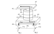
- FIG. 1 is a diagram illustrating a schematic configuration of a magnetic memory device according to one specific example.
- FIG. 1 is a diagram showing a schematic diagram of magnetic order control in a magnetoresistive element by a spin current generated in a spin Hall layer.
- FIG. 1 is a diagram showing a schematic diagram of magnetic order control in a magnetoresistive element by a spin current generated in a spin Hall layer.
- FIG. 1 is a diagram showing a schematic diagram of magnetic order control in a magnetoresistive element by a spin current generated in a spin Hall layer.
- FIG. 1 is a diagram showing a schematic diagram of magnetic order control in a magnetoresistive element by a spin current generated in a spin Hall layer.
- FIG. 1 is a diagram showing a schematic diagram of magnetic order control in a magnetoresistive element by a spin current generated in a spin Hall layer.
- FIG. 13 is a diagram illustrating a schematic configuration of a magnetic memory device according to another specific example.
- FIG. 1 is a diagram illustrating a schematic diagram of magnetic order control of a magnetoresistive element by spin transfer torque.
- FIG. 1 is a schematic diagram illustrating the configuration of a photonic spin register according to one embodiment.
- FIG. 13 is a diagram illustrating a schematic structure of a magnetoresistive effect element according to another embodiment.
- 1 is a graph showing the relationship between a magnetic field and magnetization of permalloy when a magnetic field is applied to a combined film of Mn 3 Sn and permalloy.
- 1 is a graph showing the relationship between a magnetic field and magnetization of permalloy when a magnetic field is applied to a combined film of Mn 3 Sn and permalloy.
- 1 is a graph showing the relationship between a magnetic field and magnetization of permalloy when a magnetic field is applied to a combined film of Mn 3 Sn and permalloy.
- 1 is a graph showing the relationship between a magnetic field and magnetization of permalloy when a magnetic field is applied to a combined film of Mn 3 Sn and permalloy.
- FIG. 1 shows a schematic configuration of a magnetoresistance effect element according to one embodiment.
- the magnetoresistance effect element 11 includes a free layer 13 laminated on the surface of the lower electrode layer 12, a nonmagnetic layer 14 laminated on the free layer 13, a pinned layer 15 laminated on the nonmagnetic layer 14, and a pinning layer 16 laminated on the pinned layer 15 to fix the magnetic order of the pinned layer 15 by the action of interlayer exchange coupling.
- the free layer 13 is made of an antiferromagnetic material having a reversible magnetic order.
- the pinned layer 15 functions as a reference layer that establishes a magnetic order that is fixed with respect to the free layer 13.
- the electrical resistance of the magnetoresistance effect element 11 changes to the maximum when the magnetic order of the free layer 13 is arranged parallel to the magnetic order of the pinned layer 15 and when the magnetic order of the free layer 13 is arranged antiparallel to the magnetic order of the pinned layer 15.
- the magnetic order of the free layer 13, the pinned layer 15, and the pinning layer 16 is aligned perpendicular to the interlayer interface.
- the lower electrode layer 12 is made of a conductor.
- the white arrows in the figure indicate the direction of the magnetic order.
- An upper electrode layer 17 is laminated on the pinning layer 16.
- the upper electrode layer 17 is made of a conductor.
- the upper electrode layer 17 can be made of, for example, a tantalum (Ta) layer 17a laminated on the pinning layer 16 and a ruthenium (Ru) layer 17b laminated on the tantalum layer 17a.
- the lower electrode layer 12 and the upper electrode layer 17 can introduce a current to the magnetoresistance effect element 11.
- the free layer 13 is composed of an antiferromagnetic material having a magnetic structure in which time reversal symmetry is broken macroscopically.
- Such antiferromagnetic material includes a non-collinear antiferromagnetic material.
- the antiferromagnetic material of the free layer 13 can exhibit an anomalous Hall effect based on a chiral spin structure.
- the antiferromagnetic material includes an antiferromagnetic metal containing manganese (Mn) and a collinear antiferromagnetic material having a rutile crystal structure.
- Examples of the former include Mn 3 X (X is one or more selected from the group including Sn, Ge, Ga, Rh, Pt, and Ir), Mn 3 XN (X is one or more selected from the group including Ga, Sn, and Ni), or a gamma-type Mn alloy having a face-centered cubic (fcc) structure.
- Examples of gamma-type Mn alloys include Mn1 -xFex , Mn1 -xRhx , and Mn1 -xPdx .
- Examples of the latter include RuO2 and Mn5Si3 .
- the nonmagnetic layer 14 is made of, for example, an insulator.
- the insulator include MgO , AlOx , and MgAl2O4 .
- the free layer 13, the nonmagnetic layer 14, and the pinned layer 15 (reference layer) establish a magnetic tunnel junction (MTJ).
- MTJ magnetic tunnel junction
- the magnetoresistance effect element 11 can function as a giant magnetoresistance effect (GMR) element.
- GMR giant magnetoresistance effect
- the pinned layer 15 is composed of an antiferromagnetic material.
- the antiferromagnetic material of the pinned layer 15 has a magnetic structure in which the time reversal symmetry is broken macroscopically.
- Such antiferromagnetic materials include non-collinear antiferromagnetic materials.
- the antiferromagnetic material can exhibit an anomalous Hall effect based on the chiral spin structure.
- the antiferromagnetic material includes antiferromagnetic metals containing manganese (Mn) and collinear antiferromagnetic materials having a rutile crystal structure.
- Examples of the former include Mn 3 X (X is one or more selected from the group including Sn, Ge, Ga, Rh, Pt, and Ir), Mn 3 XN (X is one or more selected from the group including Ga, Sn, and Ni), and gamma-type Mn alloys having a face-centered cubic (fcc) structure.
- Examples of gamma-type Mn alloys include Mn1 -xFex , Mn1 -xRhx , and Mn1 -xPdx .
- Examples of the latter include RuO2 and Mn5Si3 .
- the pinned layer 15 is made of the same material as the antiferromagnetic material of the free layer 13.
- the coercive force of the pinned layer 15 is set to be larger than that of the free layer 13 by the action of the pinning layer 16. As long as a magnetic structure in which time reversal symmetry is broken macroscopically is ensured, deviations in the composition ratio and the inclusion of contamination can be tolerated.
- DC sputtering can be used to deposit the free layer 13 and the pinned layer 15.
- the pressure is maintained at, for example, 0.5 Pa in an argon (Ar) atmosphere at room temperature.
- the power is set at, for example, 60 W.
- the free layer 13 and the pinned layer 15 are individually annealed at 500 degrees Celsius for, for example, 30 minutes. The annealing induces crystallization in the free layer 13 and the pinned layer 15. After annealing, the free layer 13 and the pinned layer 15 are naturally cooled to room temperature.
- the pinning layer 16 is formed of a magnetically hard antiferromagnetic material.
- antiferromagnetic materials can include manganese nitride alloy (MnN), nickel manganese alloy (NiMn), and manganese platinum alloy (MnPt).
- MnN manganese nitride alloy
- NiMn nickel manganese alloy
- MnPt manganese platinum alloy
- the antiferromagnetic material of the pinning layer 16 is deposited at room temperature on the surface of the annealed antiferromagnetic material.
- a spacer layer may be formed between the pinned layer 15 and the pinning layer 16.
- the spacer layer can be formed of, for example, Ru, Ir, W, Ti, a compound of the pinned layer 15, or a compound of the pinning layer 16.
- Ru for example, Ru, Ir, W, Ti
- a compound of the pinned layer 15 or a compound of the pinning layer 16.
- the free layer 13 is made of an antiferromagnetic material, and therefore the reversal speed of the magnetic order is faster than that of a free layer made of a ferromagnetic material. This makes it possible to reduce power consumption when reversing the magnetic order in the free layer 13.
- a hard magnetic order is established in the pinned layer 15 due to the action of interlayer exchange coupling, the change in electrical resistance resulting from the parallel and antiparallel magnetic orders created by the free layer 13 and pinned layer 15 can be well maintained.
- the coercivity of the pinned layer 15 is set to be greater than the coercivity of the free layer 13. Even if the magnetic order is reversed in the free layer 13, the magnetic order can be well maintained in the pinned layer 15.
- the pinned layer 15 can function well as a reference layer for the magnetic tunnel junction.
- the pinned layer 15 is formed from the same material as the antiferromagnetic material of the free layer 13. Even when the pinned layer 15 is made of the same material as the free layer 13, the magnetic order of the pinned layer 15 can be fixed well by the action of the pinning layer 16.
- the pinned layer 15 can function well as a reference layer for the magnetic tunnel junction.
- the pinning layer 16 is formed from an antiferromagnetic material that is magnetically harder than the antiferromagnetic material used in the pinned layer 15.
- the pinning layer 16 can effectively fix the magnetic order of the pinned layer 15.
- the pinned layer 15 can effectively function as a reference layer for the magnetic tunnel junction.
- an artificial antiferromagnetic material can be used in the pinning layer 16 of the magnetoresistance effect element 11 instead of the antiferromagnetic material described above.
- the artificial antiferromagnetic material includes a first ferromagnetic layer 18a, a spacer layer 18b stacked on the first ferromagnetic layer, and a second ferromagnetic layer 18c stacked on the spacer layer 18b.
- the first ferromagnetic layer 18a is configured as a multilayer film (Co/Pt)n with n layers of stacked cobalt (Co) layers and platinum (Pt) layers.
- the second ferromagnetic layer 18c is configured as a multilayer film (Co/Pt)m with m layers of stacked cobalt (Co) layers and platinum (Pt) layers. Other ferromagnetic materials such as CoFeB and CoFe may be used for these ferromagnetic layers.
- the spacer layer 18b is formed of a metal such as ruthenium (Ru) or iridium (Ir). The spacer layer 18b is in close contact with the first ferromagnetic layer 18a and the second ferromagnetic layer 18c. In the free layer 13, the pinned layer 15, and the pinning layer 16, the magnetic order is aligned in the direction perpendicular to the interlayer interface.
- the magnetic order may be aligned in the in-plane direction of the interlayer interface.
- the white arrows in the figures indicate the direction of the magnetic order.
- the pinning layer 16 is formed from a magnetically hard artificial antiferromagnet.
- the pinning layer 16 can effectively fix the magnetic order of the pinned layer 15.
- the pinned layer 15 can effectively function as a reference layer for the magnetic tunnel junction.
- the inventors have examined the interlayer exchange coupling between the pinned layer 15 and the pinning layer 16. For the examination, the inventors have prepared a coupling film of Mn 3 Sn [film thickness 30 nm] and NiMn [film thickness 20 nm].
- the Mn 3 Sn film was formed on a SiO 2 /Si substrate at room temperature. DC sputtering was used for the film formation. The pressure in the chamber was maintained at 0.5 [Pa] under an argon (Ar) atmosphere. The power was set to 60 [W].
- the Mn 3 Sn was annealed at 500 degrees Celsius for 30 minutes in vacuum. The Mn 3 Sn crystallized in response to the annealing. After natural cooling to room temperature, a NiMn film [20 nm thick] was deposited on the Mn 3 Sn. Co-evaporation of Mn from the K-cell and Ni from the E-gun was performed. The degree of vacuum was set to 1 ⁇ 10 ⁇ 6 [Pa]. The deposition rate of Ni was set to 0.13 [Angstroms/s]. The deposition rate of Mn was set to 0.15 [Angstroms/s].
- a 5 nm thick AlOx film was formed on the NiMn as a capping layer.
- RF sputtering was used for the film formation.
- the pressure inside the chamber was maintained at 0.2 Pa under an argon (Ar) atmosphere.
- the RF power was set to 100 W.
- the film formation rate was set to 1.6 nm/min.
- the inventors observed the crystal structure of the bonded film based on the X-ray diffraction method. As shown in FIG. 4, the peak of Mn 3 Sn was observed. On the other hand, the peak of NiMn was not observed.
- the inventors prepared a comparative example for evaluating the interlayer exchange coupling.
- a multilayer film of permalloy (Ni0.8Fe0.2) [film thickness 50 nm] and NiMn [film thickness 20 nm] was created.
- Permalloy [film thickness 50 nm] and NiMn [film thickness 20 nm] were formed in order on a SiO 2 /Si substrate at room temperature. E-gun was used to form the permalloy film.
- NiMn [film thickness 20 nm] and AlO x with a film thickness of 5 [nm] were formed in the same manner as described above. As shown in FIG. 5, in the X-ray diffraction method, the peak of permalloy (111) was observed, but the peak of NiMn was not observed.
- an anomalous Hall effect with a coercive force Hc of about 1 [T] was observed in Mn 3 Sn.
- the -B FC loop shifted toward the positive direction with the same shift amount, indicating the presence of an exchange bias.
- the inventors evaluated the magnetic coupling of the comparative multilayer film based on magnetization measurements.
- the MPMS oven option was used for the measurements.
- a shift of about 1 mT was observed in the M-H curve.
- the interface bonding energy J was calculated to be 0.036 mJ/m 2 .
- Mn3Sn film thickness 35 nm] and MnN [film thickness 30 nm].
- Mn3Sn was deposited on a SiO2 /Si substrate at room temperature. DC sputtering was used for deposition. The pressure in the chamber was maintained at 0.5 [Pa] under an argon (Ar) atmosphere. The power was set to 60 [W].
- the Mn3Sn was annealed at 500 degrees Celsius for 30 minutes in vacuum. The Mn3Sn crystallized in response to the annealing. After natural cooling to room temperature, a MnN film [30 nm thick] was deposited on the Mn3Sn . Reactive sputtering was used for deposition. The flow rate of nitrogen gas was set to 60% of the total amount of argon gas and nitrogen gas. The pressure of argon gas was set to 0.5 [Pa]. The deposition rate was set to 1.6 [nm/min].
- a 3 nm thick Al2O3 film was formed on the MnN as a capping layer.
- RF sputtering was used for the film formation.
- the chamber was maintained at a pressure of 0.2 Pa under an argon (Ar) atmosphere.
- the RF power was set to 100 W.
- the film formation rate was set to 1.6 nm/min.
- the -B FC loop shifted toward the positive direction with the same shift amount, indicating the presence of an exchange bias.
- the interface bond energy J 0.018 [mJ/m 2 ] was calculated.
- the inventors have verified the exchange bias caused by MnN.
- a non-magnetic spacer layer was laminated between Mn 3 Sn and MnN in a combined film of Mn 3 Sn [film thickness 35 nm] and MnN [film thickness 30 nm]. Tantalum (Ta) or ruthenium (Ru) was used for the spacer layer. Exchange bias was observed depending on the film thickness of the spacer layer. As shown in FIG. 12, it was confirmed that the exchange bias was reduced depending on the presence of the spacer layer. Therefore, the effect of exchange bias on MnN was confirmed.
- the inventors tried to improve the interface roughness and crystallinity with a combined film of Mn 3 Sn [film thickness 35 nm] and MnN [film thickness 30 nm].
- the inventors adopted epitaxial growth of Mn 3 Sn.
- a nonmagnetic underlayer 22 was formed on a substrate 21.
- ruthenium (Ru) was used for the underlayer 22.
- the film thickness was set to 5 [nm].
- a sapphire (0001) substrate was used for the substrate 21.
- DC sputtering was used for deposition.
- the pressure inside the chamber was maintained at 1.0 [Pa] under an argon (Ar) atmosphere.
- the power was set to 50 [W].
- the deposition rate was set to 2 [nm/min].
- the substrate 21 was heated to 700 degrees Celsius.
- a (0001) oriented ruthenium underlayer 22 was obtained by annealing for 60 minutes. The substrate 21 and underlayer 22 were then naturally cooled to room temperature.
- the Mn 3 Sn layer 23 was formed on the underlayer 22 at room temperature.
- DC sputtering was used for the film formation.
- the pressure inside the chamber was maintained at 0.5 [Pa] under an argon (Ar) atmosphere.
- the power was set to 50 [W].
- the film formation rate was set to 3 [nm/min].
- the Mn 3 Sn layer 23 was annealed at 340 degrees Celsius for 20 minutes in vacuum. The Mn 3 Sn layer 23 was crystallized in response to the anneal. Epitaxial growth of Mn 3 Sn crystal grains was realized in response to the (0001) orientation of the underlayer 22.
- the MnN layer 24 [thickness 30 nm] was deposited on the Mn 3 Sn layer 23. Reactive sputtering was used for deposition. The flow rate of nitrogen gas was set to 60% of the total amount of argon gas and nitrogen gas. The pressure of argon gas was set to 0.5 [Pa]. Then, Al 2 O 3 was deposited as a capping layer on the NiMn layer 24 to a thickness of 5 [nm]. RF sputtering was used for deposition.
- the inventors observed the crystal structure of the bonded film based on the X-ray diffraction method. As shown in Fig. 14, Mn3Sn (002) and (004) peaks and Ru (002) and (004) peaks were observed. Epitaxial growth of Mn3Sn was confirmed.
- the magnetic coupling of the MnN/Mn 3 Sn coupled film was evaluated based on the measurement of the anomalous Nernst effect.
- the -B FC loop shifted toward the positive direction with the same shift amount, indicating the presence of an exchange bias.
- the exchange bias H ex was reduced to 0.20 [T].
- the inventors observed the bias magnetic field of the Mn 3 Sn layer 23 in the MnN/Mn 3 Sn bonded film.
- the inventors changed the film thickness of the Mn 3 Sn layer 23.
- the anomalous Hall effect and the shift in the magnetic field direction were observed for all film thicknesses.
- an approximate curve was calculated from three measured values in the range of 50 nm ⁇ film thickness t ⁇ 100 nm as a function of 1/t. A decrease in the bias magnetic field was confirmed as the film thickness increased.
- an approximate curve was calculated from four measured values in the range of 35 nm ⁇ film thickness t ⁇ 100 nm as a function of 1/t. A decrease in the bias magnetic field was confirmed as the film thickness increased.
- the magnetic memory device 41 includes a magnetoresistance effect element 42 that changes the electrical resistance by reversing the magnetic order of the free layer 13 made of an antiferromagnetic material, and a spin Hall layer 43 that contacts the free layer 13 of the magnetoresistance effect element 42 and forms a current parallel to the interface of the free layer 13.
- the magnetoresistance effect element 42 like the above-mentioned magnetoresistance effect element 11, includes a free layer 13 stacked on the surface of the spin Hall layer 43, a nonmagnetic layer 14 stacked on the free layer 13, a pinned layer 15 stacked on the nonmagnetic layer 14, and a pinning layer 16 stacked on the pinned layer 15 and fixes the magnetic order of the pinned layer 15 by the action of interlayer exchange coupling.
- the free layer 13 is made of an antiferromagnetic material having a reversible magnetic order.
- the pinned layer 15 functions as a reference layer that establishes a magnetic order fixed to the free layer 13.
- the magnetoresistance effect element 42 When the magnetic order of the free layer 13 is arranged parallel to the magnetic order of the pinned layer 15, the magnetoresistance effect element 42 exhibits low electrical resistance. When the magnetic order of the free layer 13 is arranged antiparallel to the magnetic order of the pinned layer 15, the magnetoresistance effect element 42 exhibits high electrical resistance. In the free layer 13, the pinned layer 15, and the pinning layer 16, the magnetic order is aligned perpendicular to the interlayer interface.
- the spin Hall layer 43 is made of a material that exhibits the spin Hall effect (hereinafter referred to as "spin Hall material").
- spin Hall materials include nonmagnetic heavy metals, topological insulators, topological semimetals, and topological magnets.
- nonmagnetic heavy metals include tantalum (Ta), tungsten (W), and platinum (Pt).
- topological insulators include bismuth tellurium (BiTe), bismuth antimony (BiSb), and bismuth antimony tellurium (BiSbTe).
- topological semimetals include tungsten telluride (WTe 2 ) and molybdenum telluride (MoTe 2 ).
- topological magnetic materials examples include Mn3X (X is one or more elements selected from the group including Sn, Ge, Ga, Rh, Pt, and Ir), as well as cobalt manganese gallium ( Co2MnGa ), iron gallium ( Fe3Ga ), iron aluminum ( Fe3Al ), etc.
- X is one or more elements selected from the group including Sn, Ge, Ga, Rh, Pt, and Ir
- Co2MnGa iron gallium
- Fe3Ga iron aluminum
- SOT spin orbit torque
- the magnetic memory device 41 includes a first terminal 44 and a second terminal 45 that are connected to the spin Hall layer 43 and introduce a predetermined current into the spin Hall layer 43.
- the first terminal 44 and the second terminal 45 are formed, for example, from a conductive metal material.
- the first terminal 44 and the second terminal 45 are disposed apart from each other.
- a first transistor element Tr1 is connected to the first terminal 44.
- a second transistor element Tr2 is connected to the second terminal 45.
- the direction of the current between the first terminal 44 and the second terminal 45 can be selectively set by the action of the first transistor element Tr1 and the second transistor element Tr2.
- the first transistor element Tr1 is, for example, an NMOS (negative-channel metal oxide semiconductor) field effect transistor.
- the first transistor element Tr1 has a drain connected to the first terminal 44, a source connected to the first bit line BL1, and a gate connected to the word line WL.
- the second transistor element Tr2 is, for example, an NMOS field effect transistor.
- the second transistor element Tr2 has a drain connected to the second terminal 45, a source connected to the second bit line BL2, and a gate connected to the word line WL. If the potential of the first bit line BL1 is higher than that of the second bit line BL2, a current flows from the first terminal 44 to the second terminal 45. Conversely, if the potential of the second bit line BL2 is higher than that of the first bit line BL1, a current flows from the second terminal 45 to the first terminal 44.
- the magnetic memory device 41 includes a third terminal 46 that is connected to the upper electrode layer 17 of the magnetoresistance effect element 42 and introduces a current into the magnetoresistance effect element 42 in a direction perpendicular to the surface.
- the third terminal 46 is formed, for example, from a conductive metal material.
- the third terminal 46 is connected to a ground line 47 at ground potential. Therefore, a current can flow from the first terminal 44 or the second terminal 45 toward the third terminal 46.
- a current I write is supplied to the spin Hall layer 43 from the first terminal 44 and the second terminal 45.
- a high-level voltage signal is supplied to the word line WL, a voltage equal to or higher than the threshold is applied to the gate of the first transistor element Tr1 and the gate of the second transistor element Tr2.
- the first bit line BL1 is set to a high level and the second bit line BL2 is set to a low level, a current I write is introduced from the first terminal 44 to the spin Hall layer 43 and flows from the second terminal 45 to the second bit line BL2. As shown in FIG.
- the free layer 13 of the magnetoresistance effect element 42 is made of an antiferromagnetic material, and therefore the reversal speed of the magnetic order is faster than that of a free layer made of a ferromagnetic material. This makes it possible to reduce power consumption when reversing the magnetic order in the free layer 13. In addition, because a hard magnetic order is established in the pinned layer 15 due to the action of interlayer exchange coupling, the change in electrical resistance can be well maintained.
- a current I read is supplied from the second terminal 45 to the magnetoresistance effect element 42.
- a high-level voltage signal is supplied to the word line WL, the first bit line BL1 is opened, and the second bit line BL2 is set to a high level, a current I read flows from the second terminal 45 to the third terminal 46.
- the current I read is affected by the electrical resistance of the magnetoresistance effect element 42. Since a data value of "1" or "0" is assigned to a high resistance value and a low resistance value, a value of "1” or “0” can be determined by measuring the magnitude of the current I read .
- a topological insulator, a topological semimetal, or a topological magnet can be used instead of a nonmagnetic metal.
- a current is passed through the spin Hall layer 43 in one direction parallel to the plane, electrons spin-polarized parallel or oblique to the plane perpendicular direction are scattered and separated to the upper surface side (free layer 13 side) and the lower surface side of the spin Hall layer 43, generating spin accumulation.
- the spin polarization direction of the spin accumulation on the upper surface side of the spin Hall layer 43 is opposite to that of the spin accumulation on the lower surface side.
- the spin current generated in the plane perpendicular direction in this way induces SOT.
- an antiferromagnetic layer 48 may be laminated between the spin Hall layer 43 and the free layer 13.
- the antiferromagnetic layer 48 is formed of, for example, NiMn, MnN, MnPt, MnIr, FeNi, etc.
- the antiferromagnetic layer 48 can tilt the magnetic order in the free layer 13 with respect to the perpendicular direction. This allows the magnetic order in the free layer 13 to be easily inverted based on the SOT acting in the perpendicular direction.
- an antiferromagnetic material may be used in the spin Hall layer 43. Examples of the antiferromagnetic material used in the spin Hall layer 43 include NiMn, MnN, MnPt, MnIr, and FeNi. Such a spin Hall layer 43 can tilt the magnetic order in the free layer 13 with respect to the perpendicular direction.
- the magnetic memory device 51 includes a magnetoresistance effect element 52 that changes the electrical resistance by reversing the magnetic order of the free layer 13 made of an antiferromagnetic material, and a first terminal 53 and a second terminal 54 that introduce a current perpendicular to the surface of the free layer 13 of the magnetoresistance effect element 52.
- the magnetoresistance effect element 51 like the above-mentioned magnetoresistance effect element 11, includes a free layer 13 laminated on the surface of the lower electrode layer 12, a nonmagnetic layer 14 laminated on the free layer 13, a pinned layer 15 laminated on the nonmagnetic layer 14, and a pinning layer 16 laminated on the pinned layer 15 and fixing the magnetic order of the pinned layer 15 by the action of interlayer exchange coupling.
- the free layer 13 is made of an antiferromagnetic material having a reversible magnetic order.
- the pinned layer 15 functions as a reference layer that establishes a magnetic order fixed to the free layer 13.
- the magnetoresistance effect element 52 When the magnetic order of the free layer 13 is arranged parallel to the magnetic order of the pinned layer 15, the magnetoresistance effect element 52 exhibits low electrical resistance. When the magnetic order of the free layer 13 is arranged antiparallel to the magnetic order of the pinned layer 15, the magnetoresistance effect element 52 exhibits high electrical resistance. In the free layer 13, the pinned layer 15, and the pinning layer 16, the magnetic order is aligned perpendicular to the interlayer interface.
- the first terminal 53 and the second terminal 54 are formed, for example, from a conductive metal material.
- the first terminal 44 is connected, for example, to the lower electrode layer 12.
- the second terminal 45 is connected, for example, to the upper electrode layer 17.
- a transistor element Tr is connected to the first terminal 44.
- a bit line BL is connected to the second terminal 45. The presence or absence of a current between the first terminal and the second terminal can be controlled by the action of the transistor element Tr.
- the transistor element Tr is composed of, for example, an NMOS field effect transistor.
- the transistor element Tr has a drain connected to the first terminal 53, a source connected to the source line SL, and a gate connected to the word line WL. When a high-level voltage is applied to the gate from the word line WL, a current flows between the bit line BL and the source line.
- the magnetic order of the free layer 13 can be switched between parallel and anti-parallel to the magnetic order of the pinned layer 15.
- the magnetoresistance effect element 52 exhibits low electrical resistance.
- the magnetic order of the free layer 13 is arranged anti-parallel to the magnetic order of the pinned layer 15, the magnetoresistance effect element 52 exhibits high electrical resistance.
- Binary information can be distinguished based on low and high resistance.
- the parallel or anti-parallel magnetic order is assigned a data value of "1" or "0". Since the parallel or anti-parallel magnetic order is maintained without the application of voltage, data can be maintained in the magnetic memory device 51 without the supply of power.
- a current I write is supplied to the magnetoresistance effect element 52 from the first terminal 53 and the second terminal 54.
- a high-level voltage signal is supplied to the word line WL, a voltage equal to or higher than the threshold is applied to the gate of the transistor element Tr.
- the bit line BL is set to a high level and the source line SL is set to a low level, the current I write is introduced from the second terminal 54 to the magnetoresistance effect element 52 and flows from the first terminal 53 to the source line SL.
- the current I write is introduced from the first terminal 53 to the magnetoresistance effect element 52 and flows from the second terminal 54 to the bit line BL.
- the magnetic order of the free layer 13 is determined by the action of spin transfer torque (STT), and data can be written.
- STT spin transfer torque
- the data to be written can be changed depending on the direction of the current I write . In this manner, a parallel or antiparallel magnetic order is established in the free layer 13 and the pinned layer 15 .
- the free layer 13 of the magnetoresistance effect element 52 is made of an antiferromagnetic material, and therefore the reversal speed of the magnetic order is faster than that of a free layer made of a ferromagnetic material. This makes it possible to reduce power consumption when reversing the magnetic order in the free layer 13. In addition, because a hard magnetic order is established in the pinned layer 15 due to the action of interlayer exchange coupling, the change in electrical resistance can be well maintained.
- a current I read is supplied from the second terminal 54 to the magnetoresistance effect element 52.
- the bit line BL is set to a high level
- the source line SL is set to a low level
- the current I read flows from the second terminal 54 to the first terminal 53.
- the current I read is affected by the electrical resistance of the magnetoresistance effect element 52. Since a data value of "1" or “0” is assigned to a high resistance value and a low resistance value, the value of "1" or “0” can be determined by measuring the magnitude of the current I read .
- the magnetic memory devices 41 can be arranged in a matrix to form, for example, a cache memory.
- a cache memory can be connected to, for example, a processor (MPU or CPU) and used in an information processing system such as a computer system.
- the magnetic memory devices 51 can be arranged in a matrix to form, for example, a cache memory.
- FIG. 26 shows a schematic configuration of a photonic spin register 61.
- the photonic spin register 61 includes an optical receiver 62 that generates an electrical signal of serial data from an optical signal PL of serial data, and a shift register 63 that is connected to the optical receiver 62 and generates an electrical signal of parallel data from the electrical signal of serial data.
- the optical signal PL carries serial data based on pulse amplitude modulation.
- the optical receiver 62 includes a substrate 65 made of an insulator, a photoelectric conversion element 66 formed on the substrate 65 and outputting an electric signal in response to a received optical signal PL, and an optical waveguide 67 formed on the substrate 65 and guiding the optical signal PL toward the photoelectric conversion element 66.
- SiO2 is used as the insulator.
- the photoelectric conversion element 66 is formed from a dielectric (semiconductor or insulator).
- the photoelectric conversion element 66 is sandwiched on the substrate 65 between metal films 68a and 68b laminated on the substrate 65.
- the photoelectric conversion element 66 and the metal films 68a and 68b are in close contact with each other at the interface in response to the sandwiching.
- the metal films 68a and 68b are formed from, for example, Au, Ag, or other metal material.
- the metal films 68a and 68b constitute a plasmon waveguide.
- the optical waveguide 67 gradually narrows toward the photoelectric conversion element 66.
- the narrower the width of the photoelectric conversion element 66 (for example, 50 nm), the greater the light confinement effect. As a result, the light can be focused below the diffraction limit.
- the interaction between the photoelectric conversion element 66 and the optical electric field becomes stronger.
- the optical receiver 62 includes a spin Hall element 71 connected to the metal film 68b and disposed on the shift register 63.
- the spin Hall element 71 is made of a spin Hall material, similar to the spin Hall layer 43 described above.
- An electrode 72 is connected to the spin Hall element 71 at a position away from the metal film 68b. The electrode 72 is grounded.
- V bias bias voltage
- I ph photocurrent I ph flows into the spin Hall element 71 across the photoelectric conversion element 66.
- a current flows through the spin Hall element 71 parallel to the interface with the shift register 63, a spin current is generated in the perpendicular direction due to the spin Hall effect.
- the shift register 63 includes a substrate 73, a long spin Hall layer 74 laminated on the substrate 73 and extending linearly, a first magnetic layer 75 laminated on the spin Hall layer 74 and extending linearly from one end of the spin Hall layer 74 to the other end, and a second magnetic layer 76 laminated on the spin Hall layer 74, linearly continuing in series with the first magnetic layer 75 and extending to the other end of the spin Hall layer 74.
- the spin Hall layer 74 is made of a spin Hall material, similar to the spin Hall layer 43 described above.
- the linearly continuing first magnetic layer 75 and second magnetic layer 76 have magnetic domains separated by magnetic domain walls arranged in a line in the linear direction.
- the first magnetic layer 75 and the second magnetic layer 76 are composed of a topological antiferromagnet or a ferrimagnet (e.g., GdFeCo) of, for example, Mn3X (X is one or more selected from the group including Sn, Ge, Ga, Rh, Pt, and Ir).
- a topological antiferromagnet or a ferrimagnet e.g., GdFeCo
- Mn3X is one or more selected from the group including Sn, Ge, Ga, Rh, Pt, and Ir.
- the thickness of the spin Hall layer 74 is, for example, 4 [nm]
- the thicknesses of the first magnetic layer 75 and the second magnetic layer 76 are, for example, 6 [nm].
- the magnetic order is fixed in the direction perpendicular to the interface with the spin Hall layer 74 by, for example, the action of a magnet.
- the spin Hall element 71 is stacked on the magnetic domain adjacent to the second magnetic layer 76 in the first magnetic layer 75.
- a first electrode 77 is connected to the spin Hall layer 74 and the first magnetic layer 75 at one end of the spin Hall layer 74.
- a second electrode 78 is connected to the spin Hall layer 74 and the second magnetic layer 76 at the other end of the spin Hall layer 74.
- a DC shift current I s flows from the first electrode 77 to the second electrode 78.
- domain walls move in the first magnetic layer 75 and the second magnetic layer 76. When the domain walls move, the direction of the magnetic order is maintained in each magnetic domain.
- Each read element 79a, 79b, 79c, and 79d includes a barrier layer made of a nonmagnetic material (e.g., MgO) laminated on the second magnetic layer 76, a pinned layer 15 laminated on the barrier layer, a pinning layer 16 laminated on the pinned layer 15 and fixing the magnetic order of the pinned layer 15 by the action of interlayer exchange coupling, and an upper electrode layer 17 laminated on the pinning layer 16.
- An output terminal 81 is connected to the upper electrode layer 17.
- the second magnetic layer 76 is formed of an antiferromagnetic material having a magnetic order that can be reversed for each magnetic domain. Each magnetic domain is combined with the read elements 79a, 79b, 79c, and 79d to form a magnetoresistance effect element 11. Each magnetic domain functions as a free layer 13.
- the magnetic order of the first magnetic layer 75 is fixed in advance to face downward.
- the pinned layer 15 is fixed to face upward.
- the optical signal PL is guided by the optical waveguide 67 and input to the photoelectric conversion element 66.
- the optical signal PL carries serial data based on pulse amplitude modulation.
- the optical signal PL propagates as a surface plasmon polariton at the interface between the photoelectric conversion element 66 and the metal films 68a, 68b, generating a strong electric field in the vicinity.
- V bias bias voltage
- a photocurrent I ph flows from the photoelectric conversion element 66 to the spin Hall element 71.
- the SOT acts on the magnetic order.
- the photocurrent I ph is a pulse current corresponding to the "1" and "0" values contained in the optical signal PL
- the magnetic order is reversed in the magnetic domains in the first magnetic layer 75. If the current density of the photocurrent I ph does not reach the threshold value, the magnetic order is not reversed. In this way, the "1" and "0" values contained in the optical signal PL can be transferred to the spin state of the magnetic domains by the action of the photocurrent I ph .
- a read current is generated in the direction perpendicular to the surface for each of the read elements 79a, 79b, 79c, 79d.
- the read current is output from the output terminal 81.
- the magnitude of the read current changes depending on the electrical resistance determined based on the magnetoresistance effect of the magnetic tunnel junction. Therefore, a "1" value or a "0" value can be determined for each of the read elements 79a, 79b, 79c, 79d. In this way, the serial data optical signal can be converted into a parallel data electrical signal.
- FIG. 27 shows a schematic configuration of a magnetoresistance effect element according to another embodiment.
- the magnetoresistance effect element 91 includes a free layer 13 laminated on the surface of the lower electrode layer 12, a nonmagnetic layer 14 laminated on the free layer 13, a pinned layer 92 made of a ferromagnetic material laminated on the nonmagnetic layer 14, and a pinning layer 93 laminated on the pinned layer 92 and fixing the magnetic order of the pinned layer 92 by the action of interlayer exchange coupling.
- the lower electrode layer 12 is made of a conductor.
- the free layer 13 is made of an antiferromagnetic material having a reversible magnetic order.
- the free layer 13 and the nonmagnetic layer 14 are configured in the same manner as described above.
- the pinned layer 92 functions as a reference layer that establishes a magnetic order that is fixed relative to the free layer 13.
- the magnetoresistance effect element 91 exhibits low electrical resistance.
- the magnetoresistance effect element 91 exhibits high electrical resistance.
- the magnetic order is aligned in the in-plane direction of the interlayer interface.
- the white arrows in the figure indicate the direction of the magnetic order.
- An upper electrode layer 17 is laminated on the pinning layer 93. The upper electrode layer 17 is configured in the same manner as described above.
- the pinning layer 93 is made of the same material as the antiferromagnetic material of the free layer 13.
- the antiferromagnetic material of the pinning layer 93 has a magnetic structure in which the time reversal symmetry is broken macroscopically.
- Such antiferromagnetic materials include non-collinear antiferromagnetic materials.
- the antiferromagnetic material can exhibit the anomalous Hall effect based on the broken symmetry.
- Other antiferromagnetic materials include antiferromagnetic metals containing manganese (Mn) and collinear antiferromagnetic materials having a rutile crystal structure.
- Examples of the former include Mn 3 X (X is one or more selected from the group including Sn, Ge, Ga, Rh, Pt, and Ir), Mn 3 XN (X is one or more selected from the group including Ga, Sn, and Ni), or gamma-type Mn alloys with a face-centered cubic (fcc) structure.
- fcc face-centered cubic
- Examples of gamma-type Mn alloys include Mn1 -xFex , Mn1 -xRhx , and Mn1 -xPdx .
- Examples of the latter include RuO2 and Mn5Si3 .
- the coercive force of the pinned layer 92 is set to be larger than the coercive force of the free layer 13 by the action of the pinning layer 93.
- DC sputtering can be used to deposit the free layer 13 and the pinning layer 93.
- the pressure is maintained at, for example, 0.5 Pa in an argon (Ar) atmosphere at room temperature.
- the power is set to, for example, 60 W.
- the free layer 13 and the pinning layer 93 are individually annealed at 500 degrees Celsius for, for example, 30 minutes. The annealing induces crystallization in the free layer 13 and the pinning layer 93. After annealing, the free layer 13 and the pinning layer 93 are naturally cooled to room temperature.
- the free layer 13 is made of an antiferromagnetic material, and therefore the reversal speed of the magnetic order is faster than that of a free layer made of a ferromagnetic material. This makes it possible to reduce the power consumption required for reversing the magnetic order in the free layer 13.
- the change in electrical resistance can be well maintained.
- the inventors have examined the interlayer exchange coupling between the pinned layer 92 and the pinning layer 93. As shown in FIG. 28, the inventors prepared a coupling film of a Mn 3 Sn layer 94 [thickness 30 nm] and a permalloy (Ni0.8Fe0.2) layer 95 [thickness 5 nm] for the examination.
- the thickness of the Mn 3 Sn layer 94 was set to 35 [nm].
- the thickness of the permalloy layer 95 was set to 5 [nm].
- the Mn 3 Sn layer 94 was deposited at room temperature on a SiO 2 /Si substrate 96. DC sputtering was used for the deposition.
- the pressure in the chamber was maintained at 1.2 [Pa] under an argon (Ar) atmosphere.
- the power was set to 60 [W].
- the Mn 3 Sn layer 94 was annealed at 500 degrees Celsius for 30 minutes in a vacuum. The Mn 3 Sn layer 94 crystallized in response to the annealing. After natural cooling to room temperature, a permalloy layer 95 [5 nm thick] was deposited on the Mn 3 Sn layer 84. Electron beam evaporation was used for deposition. The deposition rate of permalloy was set to 0.3 [Angstroms/s].
- an AlOx layer 97 having a thickness of 5 nm was formed as a capping layer on the permalloy layer 95.
- RF sputtering was used for the film formation.
- the pressure inside the chamber was maintained at 0.2 Pa under an argon (Ar) atmosphere.
- the RF power was set to 100 W.
- the film formation rate was set to 1.6 nm/min.
- the inventors raised the temperature to 450 [K], which is sufficiently higher than the Neel temperature of Mn 3 Sn, and then applied an in-plane magnetization of +5 [T] and cooled it to 300 [K].
- 450 [K] which is sufficiently higher than the Neel temperature of Mn 3 Sn
- an in-plane magnetization of +5 [T] was measured, a shift in the positive direction was observed, which was larger than the shift in the isothermal process described above, as shown in Figure 30.
- 11 magnetoresistive effect element, 12...electrode (lower electrode layer), 13...free layer, 14...non-magnetic layer, 15...pinned layer, 16...pinning layer, 17...electrode (upper electrode layer), 41...magnetic memory device, 42...magnetoresistive effect element, 43...spin Hall layer, 51...magnetic memory device, 52...magnetoresistive effect element.
Landscapes
- Hall/Mr Elements (AREA)
- Semiconductor Memories (AREA)
- Mram Or Spin Memory Techniques (AREA)
Priority Applications (1)
| Application Number | Priority Date | Filing Date | Title |
|---|---|---|---|
| JP2024570412A JPWO2024150833A1 (https=) | 2023-01-13 | 2024-01-15 |
Applications Claiming Priority (2)
| Application Number | Priority Date | Filing Date | Title |
|---|---|---|---|
| US202363479747P | 2023-01-13 | 2023-01-13 | |
| US63/479,747 | 2023-01-13 |
Publications (1)
| Publication Number | Publication Date |
|---|---|
| WO2024150833A1 true WO2024150833A1 (ja) | 2024-07-18 |
Family
ID=91897060
Family Applications (1)
| Application Number | Title | Priority Date | Filing Date |
|---|---|---|---|
| PCT/JP2024/000871 Ceased WO2024150833A1 (ja) | 2023-01-13 | 2024-01-15 | 磁気抵抗効果素子および磁気メモリ装置 |
Country Status (2)
| Country | Link |
|---|---|
| JP (1) | JPWO2024150833A1 (https=) |
| WO (1) | WO2024150833A1 (https=) |
Citations (4)
| Publication number | Priority date | Publication date | Assignee | Title |
|---|---|---|---|---|
| JP2012151476A (ja) * | 2011-01-19 | 2012-08-09 | Crocus Technology Sa | 低電力磁気ランダムアクセスメモリセル |
| JP2014502423A (ja) * | 2010-11-17 | 2014-01-30 | ニュー・ヨーク・ユニヴァーシティ | 双極性スピン転移反転 |
| WO2017018391A1 (ja) * | 2015-07-24 | 2017-02-02 | 国立大学法人東京大学 | メモリ素子 |
| US20200341079A1 (en) * | 2019-04-23 | 2020-10-29 | Imec Vzw | Magnetic tunnel junction device |
-
2024
- 2024-01-15 WO PCT/JP2024/000871 patent/WO2024150833A1/ja not_active Ceased
- 2024-01-15 JP JP2024570412A patent/JPWO2024150833A1/ja active Pending
Patent Citations (4)
| Publication number | Priority date | Publication date | Assignee | Title |
|---|---|---|---|---|
| JP2014502423A (ja) * | 2010-11-17 | 2014-01-30 | ニュー・ヨーク・ユニヴァーシティ | 双極性スピン転移反転 |
| JP2012151476A (ja) * | 2011-01-19 | 2012-08-09 | Crocus Technology Sa | 低電力磁気ランダムアクセスメモリセル |
| WO2017018391A1 (ja) * | 2015-07-24 | 2017-02-02 | 国立大学法人東京大学 | メモリ素子 |
| US20200341079A1 (en) * | 2019-04-23 | 2020-10-29 | Imec Vzw | Magnetic tunnel junction device |
Also Published As
| Publication number | Publication date |
|---|---|
| JPWO2024150833A1 (https=) | 2024-07-18 |
Similar Documents
| Publication | Publication Date | Title |
|---|---|---|
| US6831312B2 (en) | Amorphous alloys for magnetic devices | |
| US7120049B2 (en) | Magnetic cell and magnetic memory | |
| EP0877398B1 (en) | Magnetic element and magnetic head and magnetic memory device using thereof | |
| JP3085663B2 (ja) | メモリー素子に情報を書き込む方法およびメモリー素子から情報を非破壊的に読み出す方法 | |
| US8830735B2 (en) | Magnetic memory including memory cells incorporating data recording layer with perpendicular magnetic anisotropy film | |
| CN112349832B (zh) | 磁阻效应元件以及惠斯勒合金 | |
| KR20010007428A (ko) | 자기저항 효과 소자, 자기저항 효과 메모리 셀, 및자기저항 효과 메모리셀에/로부터 정보기입 혹은 판독수행방법 | |
| JP5166600B2 (ja) | トンネル磁気記録素子、磁気メモリセル及び磁気ランダムアクセスメモリ | |
| JP3693247B2 (ja) | 磁気抵抗効果記憶素子およびその製造方法 | |
| JP2004071714A (ja) | 磁気抵抗効果素子及び磁気メモリ装置 | |
| JPWO2001024289A1 (ja) | 磁気抵抗効果記憶素子およびその製造方法 | |
| JP3691898B2 (ja) | 磁気抵抗効果素子、磁気情報読み出し方法、及び記録素子 | |
| JP4061590B2 (ja) | 磁性薄膜及びそれを用いた磁気抵抗効果素子並びに磁気デバイス | |
| JP2007201059A (ja) | 磁気素子、磁気記録装置及び書き込み方法 | |
| JP2005228998A (ja) | 磁性薄膜及びそれを用いた磁気抵抗効果素子並びに磁気デバイス | |
| KR100358452B1 (ko) | 자기 장치용 고정층 | |
| JP2005019484A (ja) | 磁気抵抗効果素子及び磁気ヘッド | |
| JP4387955B2 (ja) | 磁気抵抗効果素子 | |
| JP3520192B2 (ja) | 磁気素子とそれを用いた磁気部品および電子部品 | |
| JP2003318462A (ja) | 磁気抵抗効果素子とこれを用いた磁気ヘッドおよび磁気メモリ | |
| JP2008283173A (ja) | 磁気抵抗効果素子及び磁気メモリ装置 | |
| WO2024150833A1 (ja) | 磁気抵抗効果素子および磁気メモリ装置 | |
| JP2004031605A (ja) | 磁気抵抗効果素子および磁気メモリ装置とこれらの製造方法 | |
| CN112913003A (zh) | 磁记录层、磁畴壁移动元件和磁记录阵列 | |
| WO2023228389A1 (ja) | 磁気抵抗効果素子及び磁気抵抗効果素子の製造方法 |
Legal Events
| Date | Code | Title | Description |
|---|---|---|---|
| 121 | Ep: the epo has been informed by wipo that ep was designated in this application |
Ref document number: 24741605 Country of ref document: EP Kind code of ref document: A1 |
|
| ENP | Entry into the national phase |
Ref document number: 2024570412 Country of ref document: JP Kind code of ref document: A |
|
| WWE | Wipo information: entry into national phase |
Ref document number: 2024570412 Country of ref document: JP |
|
| NENP | Non-entry into the national phase |
Ref country code: DE |
|
| 122 | Ep: pct application non-entry in european phase |
Ref document number: 24741605 Country of ref document: EP Kind code of ref document: A1 |