WO2024150360A1 - 電子制御装置 - Google Patents
電子制御装置 Download PDFInfo
- Publication number
- WO2024150360A1 WO2024150360A1 PCT/JP2023/000575 JP2023000575W WO2024150360A1 WO 2024150360 A1 WO2024150360 A1 WO 2024150360A1 JP 2023000575 W JP2023000575 W JP 2023000575W WO 2024150360 A1 WO2024150360 A1 WO 2024150360A1
- Authority
- WO
- WIPO (PCT)
- Prior art keywords
- circuit board
- electronic control
- control device
- spring portion
- cover
- Prior art date
- Legal status (The legal status is an assumption and is not a legal conclusion. Google has not performed a legal analysis and makes no representation as to the accuracy of the status listed.)
- Ceased
Links
Images







Classifications
-
- H—ELECTRICITY
- H05—ELECTRIC TECHNIQUES NOT OTHERWISE PROVIDED FOR
- H05K—PRINTED CIRCUITS; CASINGS OR CONSTRUCTIONAL DETAILS OF ELECTRIC APPARATUS; MANUFACTURE OF ASSEMBLAGES OF ELECTRICAL COMPONENTS
- H05K7/00—Constructional details common to different types of electric apparatus
- H05K7/14—Mounting supporting structure in casing or on frame or rack
Definitions
- the present invention relates to an electronic control device.
- microcomputers i.e., multi-terminal type microcomputers.
- BGA All Grid Array
- QFP Quad Flat Package
- solder distortion occurs in the solder connections of electronic components (including BGA microcontrollers) mounted on the circuit board.
- the environmental temperature changes so that it goes back and forth between the temperature ranges of room temperature, high temperature (temperature higher than room temperature), and low temperature (temperature lower than room temperature)
- the environmental temperature changes so that it goes back and forth between the temperature ranges of room temperature, high temperature (temperature higher than room temperature), and low temperature (temperature lower than room temperature)
- the environmental temperature changes so that it goes back and forth between the temperature ranges of room temperature, high temperature (temperature higher than room temperature), and low temperature (temperature lower than room temperature)
- the above-mentioned solder distortion increases in proportion to the package size of the BGA microcontroller. For this reason, an increase in package size leads to a shortened lifespan of the solder connections.
- manufacturers are implementing various measures to extend the life of solder connections.
- Common measures include, first, optimizing the arrangement of electronic components on the circuit board, and, second, reducing the number of fastening points of the circuit board to the housing.
- the first measure is to ensure a long distance from the fastening parts of the circuit board to the mounting positions of the electronic components, thereby reducing the effect of rigid fixation to the housing and reducing solder distortion.
- the second measure is to reduce the degree of rigid fixation of the circuit board, thereby reducing solder distortion. Both measures are expected to be effective to a certain extent in reducing solder distortion.
- the size of the circuit board and therefore the size of the entire electronic control device (hereinafter also referred to as the "product size") will increase accordingly.
- the product size to which the first measure can be applied such as the difficulty of ensuring a long distance from the fastening parts of the circuit board to the mounting positions of the electronic components.
- the second measure there is a risk that the reliability of the electronic control device will decrease if the number of fastening points is reduced. For this reason, there is also a limit to how much the number of fastening points can be reduced.
- Patent Document 1 describes a technology for an electronic control device that includes a housing consisting of an upper case (cover) and a lower case (base), and a circuit board housed within the housing with electronic components mounted thereon, in which a spring portion extending from the inner surface of the upper case is brought into contact with the top surface of the circuit board, and the biasing force of this spring portion supports the circuit board.
- So-called on-board electronic control devices installed in vehicles such as automobiles are used in environments where they are susceptible to not only changes in environmental temperature but also vibrations and shocks. For example, vibrations are applied to the electronic control device while the automobile is running, and shocks are applied to the electronic control device when the automobile crashes.
- the circuit board is held down by a spring part inside the housing, but if the electronic control device is subjected to severe vibration or a large impact, the circuit board will resist the spring force of the spring part and deform the spring part, which may cause the spring part to deform excessively.
- the object of the present invention is to provide an electronic control device that can suppress excessive deformation of the spring part that holds the circuit board inside the housing.
- the present application includes multiple means for solving the above problems, and one example is an electronic control device including a circuit board on which electronic components are mounted and a housing for accommodating the circuit board.
- the housing includes a base having a pedestal for placing the circuit board, and a cover disposed opposite the base.
- the cover includes a spring portion for applying an elastic force to the circuit board in a direction for pressing the circuit board against the pedestal, and a stopper portion for restricting deformation of the spring portion to deformation within an elastic range.
- FIG. 1 is a perspective view showing an external appearance of an electronic control device according to a first embodiment
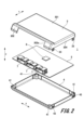
- FIG. 2 is an exploded perspective view of the electronic control device according to the first embodiment
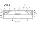
- 1 is a cross-sectional view of an electronic control device according to a first embodiment.
- 5A and 5B are diagrams illustrating a contact state between a spring portion and a circuit board in the first embodiment.
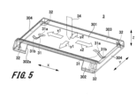
- 2 is a perspective view of a cover included in the electronic control device according to the first embodiment, seen from an oblique direction.
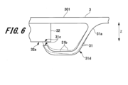
- FIG. 5A to 5C are diagrams (part 1) illustrating the positional relationship between a spring portion and a stopper portion in the electronic control device according to the first embodiment.
- FIG. 13 is a diagram (part 2) illustrating the positional relationship between the spring portion and the stopper portion in the electronic control device according to the first embodiment.
- FIG. 2 is a cross-sectional view showing an arrangement of a circuit board and a spring portion in the electronic control device according to the first embodiment.
- FIG. FIG. 11 is an exploded perspective view of an electronic control device according to a second embodiment.
- FIG. 6 is a cross-sectional view of an electronic control device according to a second embodiment.
- FIG. 6 is a cross-sectional view showing a main part of an electronic control device according to a second embodiment.
- FIG. 11 is an exploded perspective view of an electronic control device according to a third embodiment.
- FIG. 11 is a cross-sectional view of an electronic control device according to a third embodiment.
- FIG. 13A and 13B are diagrams illustrating the positional relationship between a spring portion and a stopper portion of a cover and a circuit board in an electronic control device according to a sixth embodiment.
- 13 is a diagram illustrating the structure of a spring portion of a cover in an electronic control device according to a seventh embodiment.
- FIG. 1A to 1C are diagrams showing examples of the shape of a spring portion (part 1);
- FIG. 11 is a diagram (part 2) showing an example of the shape of the spring portion.
- 11A and 11B are diagrams showing examples of the shape of the spring portion (part 3).
- Fig. 1 is a perspective view showing the external appearance of an electronic control device according to a first embodiment.
- Fig. 2 is an exploded perspective view of the electronic control device according to the first embodiment.
- Fig. 3 is a cross-sectional view of the electronic control device according to the first embodiment.
- the width direction of the electronic control device is defined as the X direction
- the depth direction of the electronic control device is defined as the Y direction
- the height direction of the electronic control device is defined as the Z direction.
- the X direction, Y direction, and Z direction are three axial directions that are orthogonal to one another.
- the electronic control device 1 includes a circuit board 5 and a housing 2 that houses the circuit board 5.
- the electronic control device 1 is, for example, an ECU (electronic control unit) that is mounted on a vehicle such as an automobile for an autonomous driving system or an advanced driving assistance system.
- the electronic control device 1 may be mounted inside the vehicle cabin or in the engine room. In this embodiment, the electronic control device 1 is assumed to be mounted inside the vehicle cabin.
- a waterproof structure for example using a waterproof adhesive, to prevent moisture from entering the inside of the electronic control device.
- the electronic control device 1 which includes a housing 2 consisting of a cover 3 and a base 4, is generally rectangular in plan view and generally rectangular in shape overall.
- the dimension (width) of the electronic control device 1 in the X direction is longer than the dimension (depth) of the electronic control device 1 in the Y direction.
- the cover 3 and the base 4 are fixed at their respective corners.
- two snap fits 33 are provided on each of the two short sides of the cover 3, and correspondingly, convex snap fit engagement portions 43 are provided on each of the two short sides of the base 4.
- the snap fits 33 are formed integrally with the cover 3, and the snap fit engagement portions 43 are formed integrally with the base 4.
- the cover 3 and the base 4 are fixed by engaging the snap fits 33 with the snap fit engagement portions 43.
- the method of fixing the cover 3 and the base 4 is not limited to a method using snap fits, and may be, for example, a method using crush ribs (not shown) or another method, although not shown.
- the cover 3 has a spring portion 31 and a stopper portion 32.
- the configuration of the cover 3 will be described in detail later.
- the base 4 has a pedestal portion 41.
- One pedestal portion 41 is formed at each of the four corners of the base 4.
- the pedestal portions 41 are provided on the base 4 for mounting the circuit board 5.
- the circuit board 5 is supported by the base 4 with the four corners of the circuit board 5 placed on the corresponding pedestal portions 41.
- the circuit board 5 is equipped with three connectors 7. These connectors 7 are components for electrically connecting the electronic control unit 1 and an external device (not shown) via a vehicle harness (not shown) to transmit and receive voltage, current, signals, and the like between the electronic control unit 1 and the external device.
- Each connector 7 is made of a resin such as PBT (polybutylene terephthalate), PA (polyamide), or PPS (polyphenylene sulfide).
- Each connector 7 also has a plurality of connector terminals (not shown) made of a metal whose main component is copper.
- Each connector 7 is connected to the circuit board 5 by, for example, soldering or press-fitting.
- the three connectors 7 are arranged along the edge of the circuit board 5. The number of connectors 7 mounted on the circuit board 5 can be changed as necessary.
- the cover 3 integrally includes an opposing wall 301, a front wall 302, a rear wall 303, and a pair of side walls 304.
- the opposing wall 301 is disposed in a state facing the circuit board 5 in the Z direction.
- the front wall 302 is disposed on the same side as the connector 7 on the circuit board 5 in the Y direction.
- the front wall 302 is formed with a cutout portion 302a (see FIG. 1 and FIG. 2).
- the cutout portion 302a is formed to avoid interference with the connector 7.
- the rear wall 303 is disposed on the opposite side of the connector 7 on the circuit board 5 in the Y direction.
- a slide core can be provided inside a molding die used for resin molding of the cover 3, and the spring portion 31 can be formed integrally with the cover 3 by moving this slide core.
- a resin material with a wide elastic range as the constituent material of the cover 3.
- a material with high toughness for example, PBT or PA rather than PPS, and it is also preferable to select a material that does not contain glass reinforced fibers.
- the cover 3 is provided with a plurality of spring portions 31 as shown in Figs. 3 and 5.
- the spring portions 31 are provided so as to be located at the ends of the circuit board 5 in the X direction and at the middle of the circuit board 5 in the Y direction.
- the spring portions 31 have a base end 31a and a free end 31b.
- the base end 31a of the spring portion 31 is connected to the opposing wall 301 of the cover 3.
- the spring portion 31 is supported at one point on the inner surface of the cover 3, and has a so-called cantilever spring shape.
- the free end 31b of the spring portion 31 is in contact with the circuit board 5 by the elastic force of the spring portion 31 itself.
- the advantage of having the spring portion 31 in a cantilever spring shape is that weld lines are less likely to occur in the spring portion 31 during resin molding.
- a weld line is a molding defect that occurs when resin that has flowed around from multiple paths joins together during molding, leaving a linear mark. Generally, the strength of the resin decreases where a weld line occurs. Therefore, by suppressing the occurrence of weld lines, a resin spring with stable strength can be achieved.
- the spring portion 31 preferably extends along the direction in which the resin flows during molding.
- a molding gate 34 is formed at a position corresponding to the center of the opposing wall 301 of the cover 3, and resin is poured from this molding gate 34 into the cavity (the hollow that forms the cover 3).
- the spring portion 31 is formed in a state in which it extends in the longitudinal directions x1, x2 of the cover 3.
- the circuit board 5 is elastically fixed by the spring portion 31.
- This type of fixing structure can be said to be a floating fixation because the circuit board 5 can be raised from the pedestal portion 41 of the base 4 by deforming the spring portion 31 against the pressing force F1 of the spring portion 31.
- a fixing structure in which the circuit board 5 is fastened to the base 4 by a screw can be said to be a rigid fixation.
- the stopper portion 32 is a portion provided to restrict deformation of the spring portion 31 to deformation in the elastic region, and has a stopper surface 32a.
- the elastic region is the elastic region of the spring portion 31 itself. Specifically, the elastic region is a region in which, even if the spring portion 31 is deformed by an external force, the spring portion 31 returns to its original shape when the external force is removed, i.e., a region in which the spring portion 31 does not undergo plastic deformation.
- the stopper portion 32 limits the amount of deformation of the spring portion 31 so that it does not deform beyond the elastic region.
- the stopper portion 32 is provided so that the spring portion 31 comes into contact with the stopper portion 32 when the spring portion 31 is deformed in the elastic region.
- the end part 31c on the free end 31b side of the spring part 31 contacts the stopper surface 32a of the stopper part 32 as shown in FIG. 6, thereby suppressing the deformation of the spring part 31.
- the tip 31c of the spring part 31 is arranged facing away from the circuit board 5 so as not to damage the board surface by contacting with the circuit board 5.
- the free end 31b of the spring portion 31 is positioned so as to protrude downward in FIG. 7 beyond the stopper portion 32 before and after the cover 3 is attached to the base 4. This allows the spring portion 31 to elastically deform while the amount of deformation of the spring portion 31 can be limited by the stopper portion 32. Furthermore, with the cover 3 attached to the base 4, the clearance C1 between the stopper portion 32 and the tip 31c of the spring portion 31 is preferably within 1 mm (excluding zero). This allows the spring portion 31 to be used stably within the elastic range.
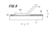
- FIG. 8 is a cross-sectional view showing the arrangement of the circuit board and the spring portion in the electronic control device according to the first embodiment.
- the circuit board 5 has a circuit pattern 52 that forms an electric circuit and an insulating film 53 that protects the circuit pattern 52.
- the circuit pattern 52 is, for example, a copper pattern
- the insulating film 53 is, for example, a resist film.
- the spring portion 31 contacts the circuit board 5 at a position different from the circuit pattern 52. Specifically, the free end 31b of the spring portion 31 contacts the insulating film 53 at a position shifted from the circuit pattern 52. Therefore, the circuit pattern 52 does not exist under the insulating film 53 with which the free end 31b of the spring portion 31 contacts.
- the circuit pattern 52 can be prevented from being broken.
- the occurrence of contamination due to sliding between the spring portion 31 and the circuit pattern 52 can be suppressed.
- the base material of the circuit board 5 can be protected.
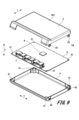
- Fig. 9 is an exploded perspective view of the electronic control device according to the second embodiment.
- Fig. 10 is a cross-sectional view of the electronic control device according to the second embodiment.
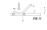
- Fig. 11 is a cross-sectional view showing a main part of the electronic control device according to the second embodiment.
- a through hole 51 is provided in the circuit board 5, but this is not limiting.
- a recess first recess
- the free end 31b of the spring portion 31 may be fitted into this recess.
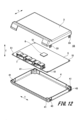
- Fig. 12 is an exploded perspective view of the electronic control device according to the third embodiment.
- Fig. 13 is a cross-sectional view of the electronic control device according to the third embodiment.
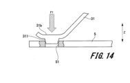
- Fig. 14 is a cross-sectional view showing a main part of the electronic control device according to the third embodiment.
- the electronic control device 1B according to the third embodiment differs from the electronic control device 1A according to the second embodiment in that a protrusion 311 is provided on the spring portion 31, and this protrusion 311 is fitted into the through hole 51 of the circuit board 5.
- the protrusion 311 corresponds to the first protrusion.
- the protrusion 311 is formed on the free end 31b of the spring portion 31.
- the protrusion 311 of the spring portion 31 is fitted into the through hole 51 of the circuit board 5, and in this state, a pressing force F1 of the spring portion 31 is applied to the circuit board 5.
- the protrusion 311 formed on the free end 31b of the spring portion 31 fits into the through hole 51 of the circuit board 5, so that the movement of the circuit board 5 in the planar direction is more firmly restricted than in the second embodiment. Therefore, it is possible to more effectively suppress the positional deviation of the circuit board 5 caused by vibrations, etc.
- a through hole 51 is provided in the circuit board 5, but this is not limiting.
- a recess first recess
- the protrusion 311 of the spring portion 31 may be fitted into this recess.
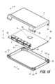
- Fig. 15 is an exploded perspective view of the electronic control device according to the fourth embodiment.
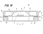
- Fig. 16 is a cross-sectional view of the electronic control device according to the fourth embodiment.
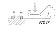
- Fig. 17 is a cross-sectional view showing a main part of the electronic control device according to the fourth embodiment.
- the electronic control device 1C according to the fourth embodiment is different from the electronic control device 1 according to the first embodiment in the constituent material of the base 4 and the support structure of the circuit board 5 by the base 4.
- the base 4 is made of the same resin as the cover 3, for example, PBT (polybutylene terephthalate), PPS (polyphenylene sulfide), PA (polyamide), etc.
- a protrusion 411 is formed on the pedestal portion 41 of the base 4.
- the protrusion 411 corresponds to the second protrusion.
- a through hole 54 is provided in the circuit board 5.
- the through hole 54 corresponds to the second hole.
- the protrusion 411 provided on the base 4 fits into the corresponding through hole 54 of the circuit board 5, and in this state, the pressing force F1 of the spring portion 31 is applied to the circuit board 5.
- the protrusions 411 formed on the pedestal portion 41 of the base 4 fit into the through holes 54 of the circuit board 5, so that movement of the circuit board 5 in the planar direction is more tightly restricted than in the first embodiment. Therefore, it is possible to effectively prevent the circuit board 5 from shifting out of position due to vibrations or the like.
- the base 4 is made of resin, it is possible to keep the difference in thermal expansion between the base 4 and the circuit board 5 small. Therefore, it is possible to reduce distortion that occurs in the solder connections of the electronic components 6, compared to when the circuit board 5 is fixed to the base 4 with screws or the like.
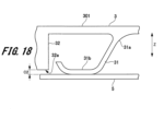
- FIG. 18 is an enlarged view of a main part of an electronic control device according to the fifth embodiment.
- the electronic control device according to the fifth embodiment is different from the electronic control device 1 according to the first embodiment in the structure for suppressing deformation of the spring portion 31 by the stopper portion 32.
- the stopper portion 32 in the first embodiment is provided such that the spring portion 31 contacts the stopper portion 32 when the spring portion 31 is deformed in the elastic region.
- the stopper portion 32 in the fifth embodiment is provided such that the circuit board 5 contacts the stopper portion 32 when the spring portion 31 is deformed in the elastic region.
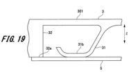
- the main surface of the circuit board 5 abuts against the stopper surface 32a of the stopper portion 32, as shown in FIG. 19. This limits the deformation of the spring portion 31 to deformation within the elastic region. This makes it possible to suppress plastic deformation of the spring portion 31.
- the spring portions 31 and the stopper portions 32 are arranged at multiple locations (four locations in the illustrated example) corresponding to the edges of the circuit board 5.
- the stopper portions 32 are arranged at positions corresponding to the four corners of the circuit board 5, and the spring portions 31 are arranged in the vicinity of the stopper portions 32.
- the sixth embodiment when a large-mass electronic component such as a connector 7 or an electrolytic capacitor 9 is mounted on the circuit board 5, it is desirable that at least one of the multiple locations where the spring portion 31 and the stopper portion 32 are arranged is near the component mounting position on the circuit board 5.
- the component mounting position on the circuit board 5 is the position where the connector 7 or the electrolytic capacitor 9 is mounted.
- the present invention is not limited to the above-described embodiment, and includes various modified examples.
- the contents of the present invention are described in detail to make it easier to understand, but the present invention is not necessarily limited to having all the configurations described in the above-described embodiment.
- a configuration is adopted in which a resin cover 3 having an integral spring portion 31 is provided, but the present invention is not limited to this.
- a configuration may be adopted in which a metal spring portion such as stainless steel is attached to a resin cover by means of screws, etc.
- the spring portion 31 has one inflection portion 31d (see FIG. 6) between the base end portion 31a and the free end 31b, but this is not limited thereto.
- the spring portion 31 may have multiple inflection portions 31d (two in the illustrated example) between the base end portion 31a and the free end 31b.
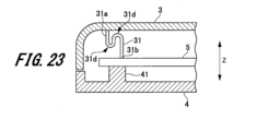
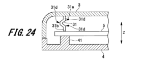
- the shape of the spring portion 31 can be modified in various ways, for example, as shown in FIG. 23 and FIG. 24.
Landscapes
- Engineering & Computer Science (AREA)
- Microelectronics & Electronic Packaging (AREA)
- Mounting Of Printed Circuit Boards And The Like (AREA)
Abstract
電子制御装置は、電子部品が実装された回路基板と、回路基板を収容する筐体と、を備える。筐体は、回路基板を据えるための台座部を有するベースと、ベースに対向して配置されるカバーと、を有する。カバーは、回路基板を台座部に押し付ける方向で回路基板に弾性力を付与するバネ部と、バネ部の変形を弾性領域での変形に抑制するためのストッパ部と、を有する。
Description
本発明は、電子制御装置に関する。
近年における自動車の電動化や電子制御装置の統合化などの動向により、自動車の電子制御装置に要求される機能が増加し、高機能なマイクロコンピュータ(以下、「マイコン」と略称する。)、つまり多端子タイプのマイコンの採用が活発化している。この流行により、マイコンのパッケージは、QFP(Quad Flat Package)タイプよりも多端子対応可能なBGA(Ball Grid Array)タイプが主流となり、パッケージサイズも拡大する傾向にある。
一方、サイズの大きいBGAパッケージのマイコン(以下、「BGAマイコン」ともいう。)を自動車の電子制御装置に適用するには、多くの課題がある。例えば、構造的な課題で代表的なものとしては、車両の環境温度が変化したときに発生する熱ストレスによってBGAマイコンの半田接続部の寿命が短くなることが挙げられる。BGAマイコンの半田接続部の短寿命化を引き起こす要因はいくつかある。そのなかのひとつの要因は、BGAマイコンが搭載された回路基板を筐体に固定する構造が、リジッドな固定であることが分かっている。リジッドな固定の典型例として、ネジを用いて回路基板を筐体に締結する構造が挙げられる。
回路基板を筐体にリジッドに固定すると、回路基板は、環境温度の変化によって凹状又は凸状に湾曲するように変形する。このように回路基板が変形すると、回路基板に実装されている電子部品(BGAマイコンを含む)の半田接続部に歪み(以下、「半田歪み」ともいう。)が発生する。また、環境温度が、常温、高温(常温よりも高い温度)、低温(常温よりも低い温度)の各温度域を行き来するように変化すると、この温度変化の繰り返しによる半田歪みによって半田接続部にクラックが発生し、最終的に断線に至ることが分かっている。また、上述した半田歪みは、BGAマイコンのパッケージサイズに比例して大きくなる。このため、パッケージサイズの拡大は、半田接続部の短寿命化につながってしまう。
これに対し、半田接続部の長寿命化を図るために、各メーカーは様々な対策を実施している。一般的な対策としては、第1に、回路基板上の電子部品の配置を最適化すること、第2に、筐体への回路基板の締結点数を削減することが挙げられる。第1の対策は、回路基板の締結部から電子部品の実装位置までの距離を長く確保することで、筐体とのリジッドな固定による影響を小さくし、半田歪みを低減させる対策となっている。第2の対策は、回路基板のリジッド固定の度合いを緩和することで、半田歪みを低減させる対策となっている。どちらの対策も、半田歪みを低減するうえでは一定の効果が見込める。ただし、第1の対策では、回路基板の締結部から電子部品の実装位置までの距離を長く確保すると、その分、回路基板のサイズ、ひいては電子制御装置全体のサイズ(以下、「製品サイズ」ともいう。)が大きくなってしまう。また、元々の製品サイズが小さい電子制御装置では、回路基板の締結部から電子部品の実装位置までの距離を長く確保することが難しいなど、第1の対策を適用できる製品サイズに制約がある。一方、第2の対策では、締結点数を減らすと電子制御装置の信頼性が低下するおそれがある。このため、締結点数を削減するにも限界がある。
そこで、電子制御装置における半田接続部の長寿命化に関する技術として、例えば、特許文献1に記載された技術が知られている。特許文献1には、上ケース(カバー)及び下ケース(ベース)からなる筐体と、電子部品を実装した状態で筐体内に収容された回路基板とを備える電子制御装置に関して、上ケースの内面から延びるバネ部を回路基板の上面に接触させ、このバネ部の付勢力によって回路基板を支持する技術が記載されている。
自動車等の車両に搭載される、いわゆる車載用の電子制御装置は、環境温度の変化だけでなく、振動や衝撃を受けやすい環境で使用される。例えば、自動車の走行中には電子制御装置に振動が加わり、自動車の衝突時には電子制御装置に衝撃が加わる。
特許文献1に記載された技術では、筐体内で回路基板をバネ部によって押さえているが、電子制御装置に激しい振動や大きな衝撃を加わった場合に、回路基板がバネ部の付勢力に抗してバネ部を変形させ、これによってバネ部が過剰に変形してしまうおそれがある。
特許文献1に記載された技術では、筐体内で回路基板をバネ部によって押さえているが、電子制御装置に激しい振動や大きな衝撃を加わった場合に、回路基板がバネ部の付勢力に抗してバネ部を変形させ、これによってバネ部が過剰に変形してしまうおそれがある。
本発明の目的は、筐体内で回路基板を押さえるバネ部の過剰な変形を抑制することができる電子制御装置を提供することにある。
上記課題を解決するために、例えば、請求の範囲に記載された構成を採用する。
本願は、上記課題を解決する手段を複数含んでいるが、その一つを挙げるならば、電子部品が実装された回路基板と、回路基板を収容する筐体と、を備える電子制御装置である。筐体は、回路基板を据えるための台座部を有するベースと、ベースに対向して配置されるカバーと、を有する。カバーは、回路基板を台座部に押し付ける方向で回路基板に弾性力を付与するバネ部と、バネ部の変形を弾性領域での変形に抑制するためのストッパ部と、を有する。
本願は、上記課題を解決する手段を複数含んでいるが、その一つを挙げるならば、電子部品が実装された回路基板と、回路基板を収容する筐体と、を備える電子制御装置である。筐体は、回路基板を据えるための台座部を有するベースと、ベースに対向して配置されるカバーと、を有する。カバーは、回路基板を台座部に押し付ける方向で回路基板に弾性力を付与するバネ部と、バネ部の変形を弾性領域での変形に抑制するためのストッパ部と、を有する。
本発明によれば、筐体内で回路基板を押さえるバネ部の過剰な変形を抑制することができる。
上記した以外の課題、構成及び効果は、以下の実施形態の説明によって明らかにされる。
上記した以外の課題、構成及び効果は、以下の実施形態の説明によって明らかにされる。
以下、本発明の実施形態について図面を参照して詳細に説明する。本明細書及び図面において、実質的に同一の機能又は構成を有する要素については、同一の符号を付し、重複する説明は省略する。
<第1実施形態>
図1は、第1実施形態に係る電子制御装置の外観を示す斜視図である。図2は、第1実施形態に係る電子制御装置の分解斜視図である。図3は、第1実施形態に係る電子制御装置の断面図である。本実施形態においては、電子制御装置を構成する各部の形状や位置関係などを明確にするために、電子制御装置の幅方向をX方向、電子制御装置の奥行き方向をY方向、電子制御装置の高さ方向をZ方向とする。X方向、Y方向及びZ方向は、互いに直交する3軸方向である。
図1は、第1実施形態に係る電子制御装置の外観を示す斜視図である。図2は、第1実施形態に係る電子制御装置の分解斜視図である。図3は、第1実施形態に係る電子制御装置の断面図である。本実施形態においては、電子制御装置を構成する各部の形状や位置関係などを明確にするために、電子制御装置の幅方向をX方向、電子制御装置の奥行き方向をY方向、電子制御装置の高さ方向をZ方向とする。X方向、Y方向及びZ方向は、互いに直交する3軸方向である。
図1~図3に示すように、電子制御装置1は、回路基板5と、回路基板5を収容する筐体2と、を備えている。電子制御装置1は、例えば、自動運転システム用又は先進運転支援システム用として、自動車などの車両に搭載されるECU(エレクトロニックコントロールユニット)である。車両における電子制御装置1の搭載場所は、車両室内でもよいし、エンジンルーム内でもよい。本実施形態においては、車両室内に搭載される電子制御装置1を想定する。エンジンルーム内に搭載される電子制御装置の場合は、電子制御装置の内部に水分が侵入しないよう、例えば防水接着剤を用いた防水構造を採用する必要がある。
筐体2は、カバー3と、ベース4とを有している。カバー3は、例えば、PBT(ポリブチレンテレフタレート)、PPS(ポリフェニレンサルファイド)、PA(ポリアミド)等の樹脂によって構成されている。ベース4は、例えば、アルミニウムや鉄等を主成分とした金属(合金を含む)によって構成されている。筐体2は、ベース4にカバー3を組み付けることによって収容空間8(図3)を形成する。収容空間8は、回路基板5を収容するために筐体2の内部に形成される空間である。
仮に、電子制御装置1がエンジンルームに搭載される場合は、カバー3、ベース4、コネクタ7の各部品間に存在する隙間に防水接着剤を塗布することにより、電子制御装置1の防水性能を確保するとよい。防水接着剤としては、例えば、シリコン系、エポキシ系、ウレタン系等の材料からなる接着剤を用いることができる。
カバー3及びベース4からなる筐体2を備える電子制御装置1は、平面視が略四角形状で、全体で略直方体形状に形成されている。電子制御装置1のX方向の寸法(幅寸法)は、電子制御装置1のY方向の寸法(奥行き寸法)よりも長い。カバー3とベース4は、それぞれの隅部で固定されている。具体的には、カバー3の2つの短辺には、それぞれ2つのスナップフィット33が設けられ、これに対応してベース4の2つの短辺には、それぞれ凸状のスナップフィット係合部43が設けられている。スナップフィット33はカバー3に一体に形成され、スナップフィット係合部43はベース4に一体に形成されている。カバー3とベース4は、スナップフィット33をスナップフィット係合部43に係合させることによって固定される。カバー3とベース4の固定方法は、スナップフィットによる固定方法に限らず、例えば図示はしないが、クラッシュリブによる固定方法でもよいし、他の固定方法でもよい。
カバー3は、図3に示すように、バネ部31と、ストッパ部32と、を有している。カバー3の構成については、後段で詳しく説明する。
ベース4は、図2及び図3に示すように、台座部41を有している。台座部41は、ベース4の四隅に1つずつ形成されている。台座部41は、回路基板5を据えるためにベース4に設けられている。回路基板5は、回路基板5の4つの隅部をそれぞれに対応する台座部41に載置した状態で、ベース4に支持される。
回路基板5は、少なくとも片面に回路パターン(図示せず)が形成されたプリント基板である。本実施形態においては、一例として、回路基板5がガラスエポキシ基板によって構成されている。回路基板5は、平面視長方形に形成されている。回路基板5の中央には電子部品6が実装されている。電子部品6は、BGAタイプのパッケージ構造を有する高機能マイコンである。
回路基板5には、3つのコネクタ7が実装されている。これらのコネクタ7は、電子制御装置1と外部装置(図示せず)とを、車両ハーネス(図示せず)を介して電気的に接続することにより、電子制御装置1と外部装置との間で電圧や電流、信号などの授受を行うための部品である。各々のコネクタ7は、例えば、PBT(ポリブチレンテレフタレート)、PA(ポリアミド)、PPS(ポリフェニレンサルファイド)等の樹脂で構成されている。また、各々のコネクタ7は、銅を主成分とした金属からなるコネクタ端子(図示せず)を複数有している。各々のコネクタ7は、例えば、半田やプレスフィットによって回路基板5に接続されている。3つのコネクタ7は、回路基板5の端辺に沿って配置されている。回路基板5に実装されるコネクタ7の数は、必要に応じて変更可能である。
なお、回路基板5には、電子部品6及びコネクタ7の他にも、例えば、トランジスタ、コンデンサ、抵抗、ダイオード、コイルなどの電子部品も実装されるが、図2及び図3ではそれらの電子部品を省略している。
次に、カバー3の構成について詳しく説明する。
カバー3は、対向壁301と、前壁302と、後壁303と、一対の側壁304と、を一体に有している。対向壁301は、Z方向で回路基板5と対向する状態に配置される。前壁302は、Y方向で回路基板5上のコネクタ7と同じ側に配置される。前壁302には切り欠き部302a(図1、図2参照)が形成されている。切り欠き部302aは、コネクタ7との干渉を避けるために形成されている。後壁303は、Y方向で回路基板5上のコネクタ7と反対側に配置される。一対の側壁304は、互いに対向する状態でX方向の一方と他方に配置される。カバー3は、対向壁301、前壁302、後壁303及び一対の側壁304の他に、前述したバネ部31及びストッパ部32を有する一体成形品である。言い換えると、バネ部31及びストッパ部32は、いずれもカバー3と一体に形成されている。その場合、バネ部31は、X方向及びY方向の各方向において、カバー3の内面から2mm以上離れた位置に配置されていることが好ましい。このようにカバー3の内面から離れた位置にバネ部31を配置することにより、カバー3の樹脂成形に使用する成形金型の内部にスライドコアを設け、このスライドコアの移動によってカバー3と一体にバネ部31を形成することができる。カバー3と一体にバネ部31を形成する場合は、カバー3の構成材料として、弾性領域の広い樹脂材料を選定することが好ましい。好ましい樹脂材料としては靭性の高い材料、例えば、PPSを選定するよりもPBT又はPAを選定することが好ましく、また、ガラス強化繊維が含まれていない材料を選定することが好ましい。
カバー3は、対向壁301と、前壁302と、後壁303と、一対の側壁304と、を一体に有している。対向壁301は、Z方向で回路基板5と対向する状態に配置される。前壁302は、Y方向で回路基板5上のコネクタ7と同じ側に配置される。前壁302には切り欠き部302a(図1、図2参照)が形成されている。切り欠き部302aは、コネクタ7との干渉を避けるために形成されている。後壁303は、Y方向で回路基板5上のコネクタ7と反対側に配置される。一対の側壁304は、互いに対向する状態でX方向の一方と他方に配置される。カバー3は、対向壁301、前壁302、後壁303及び一対の側壁304の他に、前述したバネ部31及びストッパ部32を有する一体成形品である。言い換えると、バネ部31及びストッパ部32は、いずれもカバー3と一体に形成されている。その場合、バネ部31は、X方向及びY方向の各方向において、カバー3の内面から2mm以上離れた位置に配置されていることが好ましい。このようにカバー3の内面から離れた位置にバネ部31を配置することにより、カバー3の樹脂成形に使用する成形金型の内部にスライドコアを設け、このスライドコアの移動によってカバー3と一体にバネ部31を形成することができる。カバー3と一体にバネ部31を形成する場合は、カバー3の構成材料として、弾性領域の広い樹脂材料を選定することが好ましい。好ましい樹脂材料としては靭性の高い材料、例えば、PPSを選定するよりもPBT又はPAを選定することが好ましく、また、ガラス強化繊維が含まれていない材料を選定することが好ましい。
バネ部31及びストッパ部32は、カバー3の内面から突出する状態で設けられている。具体的には、図3及び図5に示すように、バネ部31は、カバー3の対向壁301の内面から局所的に突出する状態で設けられている。また、ストッパ部32は、カバー3の全周ではなく、カバー3の対向壁301及び側壁304の内面から局所的に突出する状態で設けられている。これにより、樹脂成形時に起こりうるカバー3の反りの影響を小さくし、ストッパ部32の寸法安定性を向上させることができる。
カバー3には、図3及び図5に示すように、複数のバネ部31が設けられている。本実施形態においては、一例として、カバー3に2つのバネ部31が設けられている。バネ部31は、X方向では回路基板5の端部に位置し、Y方向では回路基板5の中間部に位置するように設けられている。バネ部31は、図3に示すように、基端部31aと、自由端31bとを有している。バネ部31の基端部31aは、カバー3の対向壁301に接続されている。つまり、バネ部31は、カバー3の内面に1点で支持された、いわゆる片持ちのバネ形状になっている。バネ部31の自由端31bは、バネ部31自身の弾性力によって回路基板5に接触している。
バネ部31を片持ちのバネ形状とした場合は、樹脂成形時にバネ部31にウェルドラインが発生しにくくなるという利点がある。ウェルドラインは、成形時に複数の経路から回り込んだ樹脂が合流することにより、線状の跡となって発生する成形不良である。一般に、ウェルドラインが発生した箇所では、樹脂の強度が低下する。よって、ウェルドラインの発生を抑制することで、安定した強度の樹脂バネを実現することができる。
また、バネ部31は、基端部31aと自由端31bとの間に1つの変曲部31d(図6参照)を有している。一般に、樹脂バネに発生する応力の緩和や耐クリープ性を向上させる方策としては、本実施形態のように樹脂バネのアーム形状に変曲部31dを設けることが効果的である。また、バネ部31に変曲部31dを設けることにより、バネ部31の弾性領域を広げて設計自由度を向上させることができる。
バネ部31は、成形時に樹脂が流れる方向に沿って延出していることが好ましい。成形金型を用いてカバー3を成形する場合は、図5に示すように、カバー3の対向壁301の中央部に対応する位置に成形ゲート34を形成し、この成形ゲート34からキャビティ(カバー3を形作る空洞)に樹脂を流し込む。このとき、一部の樹脂は、カバー3の長手方向x1,x2と短手方向y1,y2に沿って流れるのに対し、バネ部31は、カバー3の長手方向x1,x2に延出する状態で形成されている。このため、成形ゲート34からキャビティに流れ込んだ樹脂は、バネ部31を形作るキャビティの部分で、バネ部31の基端部31aから自由端31bに向かってスムーズに流れる。これにより、バネ部31にウェルドラインが発生することを効果的に抑制し、バネ部31に求められる強度を確保することができる。
バネ部31は、ベース4の台座部41に据えられた回路基板5に対して、図4に示すように、回路基板5を台座部41に押し付ける方向で回路基板5に弾性力(以下、「押し付け力」ともいう。)F1を付与する。これにより、バネ部31は、筐体2内で回路基板5を押さえている。その場合、ベース4の台座部41と回路基板5との接触界面には、バネ部31の押し付け力F1によって摩擦力F2が発生する。そうすると、X方向及びY方向を含む平面方向(以下、単に「平面方向」という。)への回路基板5の移動が規制される。また、Z方向における回路基板5の変位は、バネ部31の押し付け力F1によって抑制される。このため、回路基板5は、バネ部31によって弾性的に固定される。このような固定構造は、バネ部31の押し付け力F1に抗してバネ部31を変形させることで、ベース4の台座部41から回路基板5を浮かせることができるため、フローティング固定と言うことができる。これに対して、図示はしないが、回路基板5をネジによってベース4に締結した固定構造は、リジッド固定と言うことができる。
ストッパ部32は、バネ部31の変形を弾性領域での変形に抑制するために設けられた部分であり、ストッパ面32aを有している。弾性領域は、バネ部31自身の弾性領域である。具体的には、弾性領域は、バネ部31が外力によって変形しても、外力を取り除くとバネ部31が元に戻る領域、すなわちバネ部31が塑性変形しない領域である。ストッパ部32は、バネ部31が弾性領域を超えて変形しないようにバネ部31の変形量を制限する。ストッパ部32は、バネ部31が弾性領域で変形している状態でバネ部31がストッパ部32に接触するように設けられている。具体的には、ストッパ部32は、ストッパ部32の押し付け力F1に抗して回路基板5がバネ部31を変形させた場合に、図6に示すように、バネ部31の自由端31b側の端部(以下、「先端」ともいう。)31cがストッパ部32のストッパ面32aに接触することにより、バネ部31の変形を抑制する。これにより、バネ部31の変形を弾性領域内に抑制することができる。バネ部31の先端31cは、回路基板5との接触によって基板表面にダメージを与えないよう、回路基板5から離間する方向を向いて配置されている。
図7に示すように、バネ部31の自由端31bは、ベース4にカバー3を組み付ける前後において、ストッパ部32よりも図7の下方に突出する状態に配置される。これにより、バネ部31の弾性変形を許容しつつ、バネ部31の変形量をストッパ部32で制限することができる。また、ベース4にカバー3を組み付けた状態で、ストッパ部32とバネ部31の先端31cとの間のクリアランスC1は、好ましくは1mm以内(ただし、ゼロを除く)である。これにより、バネ部31を弾性領域内で安定して使用することができる。
図8は、第1実施形態に係る電子制御装置において、回路基板とバネ部の配置を示す断面図である。
図8に示すように、回路基板5は、電気回路を形成する回路パターン52と、回路パターン52を保護する絶縁膜53と、を有している。回路パターン52は、例えば、銅のパターンであり、絶縁膜53は、例えば、レジスト膜である。バネ部31は、回路パターン52と異なる位置で回路基板5に接触している。具体的には、バネ部31の自由端31bは、回路パターン52からずれた位置で絶縁膜53に接触している。このため、バネ部31の自由端31bが接触している絶縁膜53の下には、回路パターン52が存在していない。したがって、回路基板5の表層部がバネ部31との擦れ等によって削られた場合でも、回路パターン52の断線を避けることができる。また、バネ部31と回路パターン52との摺動に起因するコンタミネーションの発生を抑制することができる。また、バネ部31を絶縁膜53に接触させることで、回路基板5の基材を保護することができる。
図8に示すように、回路基板5は、電気回路を形成する回路パターン52と、回路パターン52を保護する絶縁膜53と、を有している。回路パターン52は、例えば、銅のパターンであり、絶縁膜53は、例えば、レジスト膜である。バネ部31は、回路パターン52と異なる位置で回路基板5に接触している。具体的には、バネ部31の自由端31bは、回路パターン52からずれた位置で絶縁膜53に接触している。このため、バネ部31の自由端31bが接触している絶縁膜53の下には、回路パターン52が存在していない。したがって、回路基板5の表層部がバネ部31との擦れ等によって削られた場合でも、回路パターン52の断線を避けることができる。また、バネ部31と回路パターン52との摺動に起因するコンタミネーションの発生を抑制することができる。また、バネ部31を絶縁膜53に接触させることで、回路基板5の基材を保護することができる。
第1実施形態に係る電子制御装置1において、例えば、回路基板5が環境温度の変化によって膨張又は収縮すると、バネ部31は、回路基板5をベース4の台座部41に押し付けつつ、回路基板5の膨張又は収縮に追従して変形する。これにより、回路基板5をベース4にリジッドに固定する場合に比べて、電子部品6の半田接続部に生じる歪みを低減することができる。したがって、電子部品6の半田接続部の寿命を延ばすことができる。
また、自動車に搭載される環境で電子制御装置1に要求される代表的な試験に衝撃試験がある。この衝撃試験において、例えば、Z方向に大きな衝撃力が加わった場合に、回路基板5がバネ部31の押し付け力F1に抗してバネ部31を変形させることが想定される。その場合、バネ部31の変形量が一定量に達すると、図6に示すようにバネ部31の先端31cがストッパ部32のストッパ面32aに突き当たる。これにより、バネ部31の変形は、弾性領域での変形に抑制される。このため、バネ部31の過剰な変形を抑制することができる。
したがって、第1実施形態に係る電子制御装置1によれば、電子部品6の半田接続部の長寿命化、並びに、バネ部31の塑性変形の抑制を同時に実現することができる。
したがって、第1実施形態に係る電子制御装置1によれば、電子部品6の半田接続部の長寿命化、並びに、バネ部31の塑性変形の抑制を同時に実現することができる。
<第2実施形態>
図9は、第2実施形態に係る電子制御装置の分解斜視図である。図10は、第2実施形態に係る電子制御装置の断面図である。図11は、第2実施形態に係る電子制御装置の要部を示す断面図である。
図9は、第2実施形態に係る電子制御装置の分解斜視図である。図10は、第2実施形態に係る電子制御装置の断面図である。図11は、第2実施形態に係る電子制御装置の要部を示す断面図である。
第2実施形態に係る電子制御装置1Aは、第1実施形態に係る電子制御装置1と比較して、バネ部31による回路基板5の固定構造が異なる。具体的には、回路基板5の4つの隅部には、貫通孔51が1つずつ設けられている。言い換えると、回路基板5には4つの貫通孔51が設けられている。貫通孔51は、第1の孔に相当する。これに対して、カバー3の対向壁301の4つのコーナー部には、バネ部31が1つずつ設けられている。言い換えると、カバー3には、4つのバネ部31が設けられている。バネ部31の自由端31bは回路基板5の貫通孔51に嵌まり合い、この状態でバネ部31の押し付け力F1が回路基板5に付与されている。
第2実施形態に係る電子制御装置1Aにおいては、回路基板5に設けられた貫通孔51にバネ部31が嵌まり合っているため、第1実施形態に比較して、平面方向への回路基板5の移動がより強固に規制される。したがって、振動等に起因する回路基板5の位置ズレを効果的に抑制することができる。
なお、本第2実施形態においては、回路基板5に貫通孔51を設けているが、これに限らず、図示はしないが、回路基板5に窪み(第1の窪み)を設け、この窪みにバネ部31の自由端31bを嵌合させた構成を採用してもよい。
<第3実施形態>
図12は、第3実施形態に係る電子制御装置の分解斜視図である。図13は、第3実施形態に係る電子制御装置の断面図である。図14は、第3実施形態に係る電子制御装置の要部を示す断面図である。
図12は、第3実施形態に係る電子制御装置の分解斜視図である。図13は、第3実施形態に係る電子制御装置の断面図である。図14は、第3実施形態に係る電子制御装置の要部を示す断面図である。
第3実施形態に係る電子制御装置1Bは、第2実施形態に係る電子制御装置1Aと比較して、バネ部31に突起311を設け、この突起311を回路基板5の貫通孔51に嵌合させた点が異なる。突起311は、第1の突起に相当する。突起311は、バネ部31の自由端31bに形成されている。バネ部31の突起311は回路基板5の貫通孔51に嵌合し、この状態でバネ部31の押し付け力F1が回路基板5に付与されている。
第3実施形態に係る電子制御装置1Bにおいては、バネ部31の自由端31bに形成された突起311が回路基板5の貫通孔51に嵌合しているため、第2実施形態に比較して、平面方向への回路基板5の移動がより強固に規制される。したがって、振動等に起因する回路基板5の位置ズレをより効果的に抑制することができる。
なお、本第3実施形態においては、回路基板5に貫通孔51を設けているが、これに限らず、図示はしないが、回路基板5に窪み(第1の窪み)を設け、この窪みにバネ部31の突起311を嵌合させた構成を採用してもよい。
<第4実施形態>
図15は、第4実施形態に係る電子制御装置の分解斜視図である。図16は、第4実施形態に係る電子制御装置の断面図である。図17は、第4実施形態に係る電子制御装置の要部を示す断面図である。
図15は、第4実施形態に係る電子制御装置の分解斜視図である。図16は、第4実施形態に係る電子制御装置の断面図である。図17は、第4実施形態に係る電子制御装置の要部を示す断面図である。
第4実施形態に係る電子制御装置1Cは、第1実施形態に係る電子制御装置1と比較して、ベース4の構成材料と、ベース4による回路基板5の支持構造が異なる。具体的には、ベース4は、カバー3と同様の樹脂、例えば、PBT(ポリブチレンテレフタレート)、PPS(ポリフェニレンサルファイド)、PA(ポリアミド)等の樹脂によって構成されている。また、ベース4の台座部41には突起411が形成されている。突起411は、第2の突起に相当する。一方、回路基板5には、貫通孔54が設けられている。貫通孔54は、第2の孔に相当する。ベース4に設けられた突起411は、これに対応する回路基板5の貫通孔54に嵌まり合い、この状態でバネ部31の押し付け力F1が回路基板5に付与されている。
第4実施形態に係る電子制御装置1Cにおいては、ベース4の台座部41に形成された突起411が回路基板5の貫通孔54に嵌合しているため、第1実施形態に比較して、平面方向への回路基板5の移動がより強固に規制される。したがって、振動等に起因する回路基板5の位置ズレを効果的に抑制することができる。また、ベース4は樹脂によって構成されているため、ベース4と回路基板5との熱膨張差を小さく抑えることができる。したがって、回路基板5をベース4にネジ等で固定する場合に比べて、電子部品6の半田接続部に生じる歪みを低減することができる。
なお、本第4実施形態においては、回路基板5に貫通孔54を設けているが、これに限らず、図示はしないが、回路基板5に窪み(第2の窪み)を設け、この窪みにベース4の突起411を嵌合させた構成を採用してもよい。
<第5実施形態>
図18は、第5実施形態に係る電子制御装置の要部を拡大した図である。
第5実施形態に係る電子制御装置は、第1実施形態に係る電子制御装置1と比較して、ストッパ部32によるバネ部31の変形抑制構造が異なる。具体的には、第1実施形態におけるストッパ部32は、バネ部31が弾性領域で変形している状態でバネ部31がストッパ部32に接触するように設けられている。これに対して、第5実施形態におけるストッパ部32は、バネ部31が弾性領域で変形している状態で回路基板5がストッパ部32に接触するように設けられている。
図18は、第5実施形態に係る電子制御装置の要部を拡大した図である。
第5実施形態に係る電子制御装置は、第1実施形態に係る電子制御装置1と比較して、ストッパ部32によるバネ部31の変形抑制構造が異なる。具体的には、第1実施形態におけるストッパ部32は、バネ部31が弾性領域で変形している状態でバネ部31がストッパ部32に接触するように設けられている。これに対して、第5実施形態におけるストッパ部32は、バネ部31が弾性領域で変形している状態で回路基板5がストッパ部32に接触するように設けられている。
図18に示すように、バネ部31の自由端31bは、ベース4にカバー3を組み付ける前後において、ストッパ部32よりも図18の下方に突出する状態に配置される。これにより、バネ部31の弾性変形を許容しつつ、バネ部31の変形量をストッパ部32で制限することができる。また、ベース4にカバー3を組み付けた状態で、ストッパ部32と回路基板5との間のクリアランスC2は、好ましくは1mm以内(ただし、ゼロを除く)である。これにより、バネ部31を弾性領域内で安定して使用することができる。
第5実施形態に係る電子制御装置において、例えば外部から加わる衝撃力によって回路基板5がバネ部31を変形させ、これによってバネ部31の変形量が一定量に達すると、図19に示すように回路基板5の主面がストッパ部32のストッパ面32aに突き当たる。これにより、バネ部31の変形は、弾性領域での変形に制限される。このため、バネ部31の塑性変形を抑制することができる。
<第6実施形態>
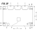
図20は、第6実施形態に係る電子制御装置において、カバーが有するバネ部及びストッパ部と回路基板との位置関係を説明する図である。なお、第6実施形態においては、上記第5実施形態と同様に、回路基板5がストッパ部32に接触することでバネ部31の変形が抑制される構成を採用している。
図20は、第6実施形態に係る電子制御装置において、カバーが有するバネ部及びストッパ部と回路基板との位置関係を説明する図である。なお、第6実施形態においては、上記第5実施形態と同様に、回路基板5がストッパ部32に接触することでバネ部31の変形が抑制される構成を採用している。
図20に示すように、ストッパ部32は、バネ部31の近傍に配置されている。本実施形態においては、一例として、バネ部31とストッパ部32がY方向で隣接するように配置されている。この場合、Y方向で隣り合うバネ部31とストッパ部32の中心間距離をL1(mm)とし、回路基板5の短手寸法をL2(mm)すると、L1は、好ましくは、L2の1/3以下であり、より好ましくは、L2の1/4以下であり、さらに好ましくは、L2の1/5以下である。このようにバネ部31の近傍にストッパ部32を配置することにより、ストッパ部32によって抑制されるバネ部31の変形量が想定しやくなる。よって、電子制御装置の設計が容易になる。
また、第6実施形態において、バネ部31及びストッパ部32は、回路基板5の端辺に対応する複数の箇所(図例では4箇所)に配置されている。本実施形態においては、一例として、回路基板5の四隅に対応する位置にストッパ部32が配置され、このストッパ部32の近傍にバネ部31が配置されている。このようにバネ部31及びストッパ部32を配置することにより、複数のバネ部31の弾性力によって回路基板5をバランス良く固定することができる。また、回路基板5における部品実装効率を高めて、電子制御装置の小型化に寄与することができる。
また、第6実施形態において、回路基板5にコネクタ7や電解コンデンサ9のような質量の大きい電子部品が実装されている場合、バネ部31及びストッパ部32が配置されている複数の箇所のうち少なくともいずれか1つの箇所は、回路基板5における部品実装位置の近傍であることが望ましい。本実施形態において、回路基板5における部品実装位置は、コネクタ7が実装されている位置や、電解コンデンサ9が実装されている位置である。このようにバネ部31及びストッパ部32を配置することにより、Z方向に大きな衝撃力が加わった場合に、コネクタ7や電解コンデンサ9の重さによる回路基板5の変位や、これにともなうバネ部31の変形を、ストッパ部32によって効果的に抑制することができる。
なお、本第6実施形態においては、回路基板5における部品実装位置の近傍にバネ部31及びストッパ部32を配置しているが、これに限らず、回路基板5の重心位置の近傍にバネ部31及びストッパ部32を配置してもよい。
<第7実施形態>
図21は、第7実施形態に係る電子制御装置において、カバーが有するバネ部の構造を説明する図である。
図21に示すように、バネ部31は、カバー3の対向壁301に接続された2つの基端部31aと、回路基板5に押し当てられる自由端31bと、2つの変曲部31dとを有している。バネ部31は、カバー3の内面に2点で支持された、いわゆる両持ちのバネ形状になっている。樹脂バネは、材料の特性上、一定の荷重を継続的に付与することにより、徐々に変形が進んでいく特性、すなわちクリープ特性を有する。一般的にクリープ耐性は、材料特性や樹脂部品の形状に依存する。本実施形態のように両持ちのバネ形状を採用すると、片持ちのバネ形状に比べて、耐クリープ性を向上させることができる。
<変形例等>
本発明は、上述した実施形態に限定されるものではなく、様々な変形例を含む。例えば、上述した実施形態では、本発明の内容を理解しやすいように詳細に説明しているが、本発明は、上述した実施形態で説明したすべての構成を必ずしも備えるものに限定されない。また、ある実施形態の構成の一部を、他の実施形態の構成に置き換えることが可能である。また、ある実施形態の構成に他の実施形態の構成を加えることも可能である。また、各実施形態の構成の一部について、これを削除し、又は他の構成を追加し、あるいは他の構成に置換することも可能である。
本発明は、上述した実施形態に限定されるものではなく、様々な変形例を含む。例えば、上述した実施形態では、本発明の内容を理解しやすいように詳細に説明しているが、本発明は、上述した実施形態で説明したすべての構成を必ずしも備えるものに限定されない。また、ある実施形態の構成の一部を、他の実施形態の構成に置き換えることが可能である。また、ある実施形態の構成に他の実施形態の構成を加えることも可能である。また、各実施形態の構成の一部について、これを削除し、又は他の構成を追加し、あるいは他の構成に置換することも可能である。
また、上記実施形態においては、バネ部31を一体に有する樹脂製のカバー3を備えた構成を採用しているが、本発明はこれに限らず、例えば、ステンレス等の金属製のバネ部を、樹脂製のカバーにネジ止め等によって取り付けた構成を採用してもよい。
また、上記実施形態において、バネ部31は、基端部31aと自由端31bとの間に1つの変曲部31d(図6参照)を有しているが、これに限らず、例えば図22に示すように、バネ部31は、基端部31aと自由端31bとの間に複数(図例では2つ)の変曲部31dを有していてもよい。変曲部31dの数を増やすことで、バネ部31の弾性領域を更に広げることができる。また、バネ部31の形状は、例えば図23及び図24に示すように、種々の変更が可能である。
1,1A,1B,1C…電子制御装置、2…筐体、3…カバー、4…ベース、5…回路基板、6…電子部品、31…バネ部、31a…基端部、31b…自由端、31d…変曲部、32…ストッパ部、41…台座部、51…貫通孔(第1の孔)、52…回路パターン、54…貫通孔(第2の孔)、311…突起(第1の突起)、411…突起(第2の突起)
Claims (17)
- 電子部品が実装された回路基板と、前記回路基板を収容する筐体と、を備え、
前記筐体は、前記回路基板を据えるための台座部を有するベースと、前記ベースに対向して配置されるカバーと、を有し、
前記カバーは、前記回路基板を前記台座部に押し付ける方向で前記回路基板に弾性力を付与するバネ部と、前記バネ部の変形を弾性領域での変形に抑制するためのストッパ部と、を有する
電子制御装置。 - 前記ストッパ部は、前記バネ部が弾性領域で変形している状態で前記バネ部が前記ストッパ部に接触するように設けられている
請求項1に記載の電子制御装置。 - 前記ストッパ部は、前記バネ部が弾性領域で変形している状態で前記回路基板が前記ストッパ部に接触するように設けられている
請求項1に記載の電子制御装置。 - 前記バネ部の自由端は、前記ベースに前記カバーを組み付ける前後において、前記ストッパ部よりも突出する状態に配置される
請求項2又は3に記載の電子制御装置。 - 前記ベースに前記カバーを組み付けた状態で、前記ストッパ部と前記回路基板との間のクリアランス、又は、前記ストッパ部と前記バネ部の先端との間のクリアランスが1mm以内である
請求項4に記載の電子制御装置。 - 前記ストッパ部は、前記バネ部の近傍に配置されている
請求項1に記載の電子制御装置。 - 前記ストッパ部は、前記カバーの内面から局所的に突出する状態で設けられている
請求項1に記載の電子制御装置。 - 前記バネ部及び前記ストッパ部は、前記回路基板の端辺に対応する複数の箇所に配置されている
請求項1に記載の電子制御装置。 - 前記複数の箇所のうち少なくともいずれか1つの箇所は、前記回路基板における部品実装位置又は前記回路基板の重心位置の近傍である
請求項8に記載の電子制御装置。 - 前記回路基板は、前記バネ部と嵌まり合う第1の孔又は第1の窪みを有する
請求項1に記載の電子制御装置。 - 前記バネ部は、前記第1の孔又は前記第1の窪みに嵌合する第1の突起を有する
請求項10に記載の電子制御装置。 - 前記ベースは、樹脂製のベースであるとともに、前記台座部に第2の突起を有し、
前記回路基板は、前記第2の突起に嵌まり合う第2の孔又は第2の窪みを有する
請求項1に記載の電子制御装置。 - 前記バネ部は、前記バネ部の基端部と自由端との間に、少なくとも1つの変曲部を有する
請求項1に記載の電子制御装置。 - 前記バネ部は、前記カバーの内面に1点又は2点で支持されている
請求項7に記載の電子制御装置。 - 前記カバーは、前記バネ部を有する樹脂の一体成形品であり、
前記バネ部は、成形時に樹脂が流れる方向に沿って延出している
請求項1に記載の電子制御装置。 - 前記バネ部は、前記カバーの内面から2mm以上離れた位置に配置されている
請求項15に記載の電子制御装置。 - 前記回路基板は、回路パターンを有し、
前記バネ部は、前記回路パターンと異なる位置で前記回路基板に接触している
請求項1に記載の電子制御装置。
Priority Applications (1)
| Application Number | Priority Date | Filing Date | Title |
|---|---|---|---|
| PCT/JP2023/000575 WO2024150360A1 (ja) | 2023-01-12 | 2023-01-12 | 電子制御装置 |
Applications Claiming Priority (1)
| Application Number | Priority Date | Filing Date | Title |
|---|---|---|---|
| PCT/JP2023/000575 WO2024150360A1 (ja) | 2023-01-12 | 2023-01-12 | 電子制御装置 |
Publications (1)
| Publication Number | Publication Date |
|---|---|
| WO2024150360A1 true WO2024150360A1 (ja) | 2024-07-18 |
Family
ID=91896528
Family Applications (1)
| Application Number | Title | Priority Date | Filing Date |
|---|---|---|---|
| PCT/JP2023/000575 Ceased WO2024150360A1 (ja) | 2023-01-12 | 2023-01-12 | 電子制御装置 |
Country Status (1)
| Country | Link |
|---|---|
| WO (1) | WO2024150360A1 (ja) |
Citations (4)
| Publication number | Priority date | Publication date | Assignee | Title |
|---|---|---|---|---|
| KR100504659B1 (ko) * | 2003-02-11 | 2005-08-03 | 현대모비스 주식회사 | 차량의 인쇄회로기판 설치 구조 |
| JP2006066623A (ja) * | 2004-08-26 | 2006-03-09 | Denso Corp | 電子制御装置 |
| JP2018064015A (ja) * | 2016-10-12 | 2018-04-19 | アイシン・エィ・ダブリュ株式会社 | 基板保持装置 |
| JP2019161194A (ja) * | 2018-03-16 | 2019-09-19 | パナソニックIpマネジメント株式会社 | 電子機器用ケース及び電子機器 |
-
2023
- 2023-01-12 WO PCT/JP2023/000575 patent/WO2024150360A1/ja not_active Ceased
Patent Citations (4)
| Publication number | Priority date | Publication date | Assignee | Title |
|---|---|---|---|---|
| KR100504659B1 (ko) * | 2003-02-11 | 2005-08-03 | 현대모비스 주식회사 | 차량의 인쇄회로기판 설치 구조 |
| JP2006066623A (ja) * | 2004-08-26 | 2006-03-09 | Denso Corp | 電子制御装置 |
| JP2018064015A (ja) * | 2016-10-12 | 2018-04-19 | アイシン・エィ・ダブリュ株式会社 | 基板保持装置 |
| JP2019161194A (ja) * | 2018-03-16 | 2019-09-19 | パナソニックIpマネジメント株式会社 | 電子機器用ケース及び電子機器 |
Similar Documents
| Publication | Publication Date | Title |
|---|---|---|
| CN101145641B (zh) | 配线基板收纳结构 | |
| US7891983B2 (en) | Contact and IC socket using the same | |
| US6442027B2 (en) | Electronic control unit having connector positioned between two circuit substrates | |
| JP4943930B2 (ja) | 立体回路部品の取付構造 | |
| EP1895823B1 (en) | Circuit Board Housing Structure | |
| CN114041245B (zh) | 连接器和电子设备 | |
| WO2020079801A1 (ja) | 基板収納筐体 | |
| KR20200119838A (ko) | 커넥터 및 전자 기기 | |
| JP2012099267A (ja) | 端子およびこれを用いたコネクタ | |
| JP7010555B2 (ja) | フローティングコネクタ | |
| WO2022009902A1 (ja) | コネクタ及び電子機器 | |
| US7896693B2 (en) | Retaining member electric component and electric device | |
| JP2019009183A (ja) | 半導体装置 | |
| JP4866830B2 (ja) | 自動車用電子装置 | |
| CN112803180B (zh) | 逆变器装置 | |
| JP2013149899A (ja) | 電子制御ユニットのケース | |
| CA2742558A1 (en) | Flat cable wiring structure | |
| JP4820241B2 (ja) | 配線基板収納構造 | |
| JP5044471B2 (ja) | コネクタ | |
| JP4549406B2 (ja) | 電子部品搭載構造及び車載用センサー | |
| JP5769589B2 (ja) | フラット回路体のコネクタ接続構造 | |
| JP7224789B2 (ja) | 車両用電子制御装置 | |
| JP7200481B2 (ja) | 電子装置 | |
| JP2017208273A (ja) | 電子装置 | |
| KR102934917B1 (ko) | 커넥터 및 전자 기기 |
Legal Events
| Date | Code | Title | Description |
|---|---|---|---|
| 121 | Ep: the epo has been informed by wipo that ep was designated in this application |
Ref document number: 23915982 Country of ref document: EP Kind code of ref document: A1 |
|
| NENP | Non-entry into the national phase |
Ref country code: DE |
|
| 122 | Ep: pct application non-entry in european phase |
Ref document number: 23915982 Country of ref document: EP Kind code of ref document: A1 |
|
| NENP | Non-entry into the national phase |
Ref country code: JP |