WO2024142970A1 - 照明光学系、露光装置、及びデバイス製造方法 - Google Patents
照明光学系、露光装置、及びデバイス製造方法 Download PDFInfo
- Publication number
- WO2024142970A1 WO2024142970A1 PCT/JP2023/044847 JP2023044847W WO2024142970A1 WO 2024142970 A1 WO2024142970 A1 WO 2024142970A1 JP 2023044847 W JP2023044847 W JP 2023044847W WO 2024142970 A1 WO2024142970 A1 WO 2024142970A1
- Authority
- WO
- WIPO (PCT)
- Prior art keywords
- light
- illumination
- optical system
- emitting
- illumination optical
- Prior art date
- Legal status (The legal status is an assumption and is not a legal conclusion. Google has not performed a legal analysis and makes no representation as to the accuracy of the status listed.)
- Ceased
Links
Images


Classifications
-
- G—PHYSICS
- G03—PHOTOGRAPHY; CINEMATOGRAPHY; ANALOGOUS TECHNIQUES USING WAVES OTHER THAN OPTICAL WAVES; ELECTROGRAPHY; HOLOGRAPHY
- G03F—PHOTOMECHANICAL PRODUCTION OF TEXTURED OR PATTERNED SURFACES, e.g. FOR PRINTING, FOR PROCESSING OF SEMICONDUCTOR DEVICES; MATERIALS THEREFOR; ORIGINALS THEREFOR; APPARATUS SPECIALLY ADAPTED THEREFOR
- G03F7/00—Photomechanical, e.g. photolithographic, production of textured or patterned surfaces, e.g. printing surfaces; Materials therefor, e.g. comprising photoresists; Apparatus specially adapted therefor
- G03F7/70—Microphotolithographic exposure; Apparatus therefor
- G03F7/70058—Mask illumination systems
- G03F7/70191—Optical correction elements, filters or phase plates for controlling intensity, wavelength, polarisation, phase or the like
-
- G—PHYSICS
- G03—PHOTOGRAPHY; CINEMATOGRAPHY; ANALOGOUS TECHNIQUES USING WAVES OTHER THAN OPTICAL WAVES; ELECTROGRAPHY; HOLOGRAPHY
- G03F—PHOTOMECHANICAL PRODUCTION OF TEXTURED OR PATTERNED SURFACES, e.g. FOR PRINTING, FOR PROCESSING OF SEMICONDUCTOR DEVICES; MATERIALS THEREFOR; ORIGINALS THEREFOR; APPARATUS SPECIALLY ADAPTED THEREFOR
- G03F7/00—Photomechanical, e.g. photolithographic, production of textured or patterned surfaces, e.g. printing surfaces; Materials therefor, e.g. comprising photoresists; Apparatus specially adapted therefor
- G03F7/70—Microphotolithographic exposure; Apparatus therefor
- G03F7/70058—Mask illumination systems
- G03F7/70075—Homogenization of illumination intensity in the mask plane by using an integrator, e.g. fly's eye lens, facet mirror or glass rod, by using a diffusing optical element or by beam deflection
-
- G—PHYSICS
- G03—PHOTOGRAPHY; CINEMATOGRAPHY; ANALOGOUS TECHNIQUES USING WAVES OTHER THAN OPTICAL WAVES; ELECTROGRAPHY; HOLOGRAPHY
- G03F—PHOTOMECHANICAL PRODUCTION OF TEXTURED OR PATTERNED SURFACES, e.g. FOR PRINTING, FOR PROCESSING OF SEMICONDUCTOR DEVICES; MATERIALS THEREFOR; ORIGINALS THEREFOR; APPARATUS SPECIALLY ADAPTED THEREFOR
- G03F7/00—Photomechanical, e.g. photolithographic, production of textured or patterned surfaces, e.g. printing surfaces; Materials therefor, e.g. comprising photoresists; Apparatus specially adapted therefor
- G03F7/20—Exposure; Apparatus therefor
-
- G—PHYSICS
- G03—PHOTOGRAPHY; CINEMATOGRAPHY; ANALOGOUS TECHNIQUES USING WAVES OTHER THAN OPTICAL WAVES; ELECTROGRAPHY; HOLOGRAPHY
- G03F—PHOTOMECHANICAL PRODUCTION OF TEXTURED OR PATTERNED SURFACES, e.g. FOR PRINTING, FOR PROCESSING OF SEMICONDUCTOR DEVICES; MATERIALS THEREFOR; ORIGINALS THEREFOR; APPARATUS SPECIALLY ADAPTED THEREFOR
- G03F7/00—Photomechanical, e.g. photolithographic, production of textured or patterned surfaces, e.g. printing surfaces; Materials therefor, e.g. comprising photoresists; Apparatus specially adapted therefor
- G03F7/70—Microphotolithographic exposure; Apparatus therefor
- G03F7/70008—Production of exposure light, i.e. light sources
- G03F7/70025—Production of exposure light, i.e. light sources by lasers
-
- G—PHYSICS
- G03—PHOTOGRAPHY; CINEMATOGRAPHY; ANALOGOUS TECHNIQUES USING WAVES OTHER THAN OPTICAL WAVES; ELECTROGRAPHY; HOLOGRAPHY
- G03F—PHOTOMECHANICAL PRODUCTION OF TEXTURED OR PATTERNED SURFACES, e.g. FOR PRINTING, FOR PROCESSING OF SEMICONDUCTOR DEVICES; MATERIALS THEREFOR; ORIGINALS THEREFOR; APPARATUS SPECIALLY ADAPTED THEREFOR
- G03F7/00—Photomechanical, e.g. photolithographic, production of textured or patterned surfaces, e.g. printing surfaces; Materials therefor, e.g. comprising photoresists; Apparatus specially adapted therefor
- G03F7/70—Microphotolithographic exposure; Apparatus therefor
- G03F7/70008—Production of exposure light, i.e. light sources
- G03F7/7005—Production of exposure light, i.e. light sources by multiple sources, e.g. light-emitting diodes [LED] or light source arrays
-
- G—PHYSICS
- G03—PHOTOGRAPHY; CINEMATOGRAPHY; ANALOGOUS TECHNIQUES USING WAVES OTHER THAN OPTICAL WAVES; ELECTROGRAPHY; HOLOGRAPHY
- G03F—PHOTOMECHANICAL PRODUCTION OF TEXTURED OR PATTERNED SURFACES, e.g. FOR PRINTING, FOR PROCESSING OF SEMICONDUCTOR DEVICES; MATERIALS THEREFOR; ORIGINALS THEREFOR; APPARATUS SPECIALLY ADAPTED THEREFOR
- G03F7/00—Photomechanical, e.g. photolithographic, production of textured or patterned surfaces, e.g. printing surfaces; Materials therefor, e.g. comprising photoresists; Apparatus specially adapted therefor
- G03F7/70—Microphotolithographic exposure; Apparatus therefor
- G03F7/70058—Mask illumination systems
- G03F7/7015—Details of optical elements
- G03F7/70166—Capillary or channel elements, e.g. nested extreme ultraviolet [EUV] mirrors or shells, optical fibers or light guides
-
- G—PHYSICS
- G03—PHOTOGRAPHY; CINEMATOGRAPHY; ANALOGOUS TECHNIQUES USING WAVES OTHER THAN OPTICAL WAVES; ELECTROGRAPHY; HOLOGRAPHY
- G03F—PHOTOMECHANICAL PRODUCTION OF TEXTURED OR PATTERNED SURFACES, e.g. FOR PRINTING, FOR PROCESSING OF SEMICONDUCTOR DEVICES; MATERIALS THEREFOR; ORIGINALS THEREFOR; APPARATUS SPECIALLY ADAPTED THEREFOR
- G03F7/00—Photomechanical, e.g. photolithographic, production of textured or patterned surfaces, e.g. printing surfaces; Materials therefor, e.g. comprising photoresists; Apparatus specially adapted therefor
- G03F7/70—Microphotolithographic exposure; Apparatus therefor
- G03F7/70058—Mask illumination systems
- G03F7/70208—Multiple illumination paths, e.g. radiation distribution devices, microlens illumination systems, multiplexers or demultiplexers for single or multiple projection systems
-
- G—PHYSICS
- G03—PHOTOGRAPHY; CINEMATOGRAPHY; ANALOGOUS TECHNIQUES USING WAVES OTHER THAN OPTICAL WAVES; ELECTROGRAPHY; HOLOGRAPHY
- G03F—PHOTOMECHANICAL PRODUCTION OF TEXTURED OR PATTERNED SURFACES, e.g. FOR PRINTING, FOR PROCESSING OF SEMICONDUCTOR DEVICES; MATERIALS THEREFOR; ORIGINALS THEREFOR; APPARATUS SPECIALLY ADAPTED THEREFOR
- G03F7/00—Photomechanical, e.g. photolithographic, production of textured or patterned surfaces, e.g. printing surfaces; Materials therefor, e.g. comprising photoresists; Apparatus specially adapted therefor
- G03F7/70—Microphotolithographic exposure; Apparatus therefor
- G03F7/70216—Mask projection systems
- G03F7/70358—Scanning exposure, i.e. relative movement of patterned beam and workpiece during imaging
-
- G—PHYSICS
- G03—PHOTOGRAPHY; CINEMATOGRAPHY; ANALOGOUS TECHNIQUES USING WAVES OTHER THAN OPTICAL WAVES; ELECTROGRAPHY; HOLOGRAPHY
- G03F—PHOTOMECHANICAL PRODUCTION OF TEXTURED OR PATTERNED SURFACES, e.g. FOR PRINTING, FOR PROCESSING OF SEMICONDUCTOR DEVICES; MATERIALS THEREFOR; ORIGINALS THEREFOR; APPARATUS SPECIALLY ADAPTED THEREFOR
- G03F7/00—Photomechanical, e.g. photolithographic, production of textured or patterned surfaces, e.g. printing surfaces; Materials therefor, e.g. comprising photoresists; Apparatus specially adapted therefor
- G03F7/70—Microphotolithographic exposure; Apparatus therefor
- G03F7/70483—Information management; Active and passive control; Testing; Wafer monitoring, e.g. pattern monitoring
- G03F7/7055—Exposure light control in all parts of the microlithographic apparatus, e.g. pulse length control or light interruption
Definitions
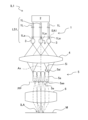
- FIG. 9 is a diagram showing the positional relationship between an end face of an optical fiber and a collector lens in a light source section of an illumination optical system according to a modified example of the first embodiment.
- FIG. 10(a) is a diagram showing an optical path when only the output end of the normal illumination fiber is emitting light in the illumination optical system of the second embodiment of the present invention, and
- FIG. 10(b) shows an image formed on the entrance surface of the fly's eye lens by light from the normal illumination fiber.
- FIG. 11 is a diagram showing a schematic configuration of a fiber group of a light source unit according to the second embodiment.
- FIG. 12 is a diagram showing an arrangement of a plurality of light emitting surfaces in a light emitting region of a light source unit according to the second embodiment.
- FIG. 15 is a diagram showing the arrangement of an exit end of an optical fiber, an axicon lens, a collector lens, and two relay lenses in a light source section of an illumination optical system according to a modified example.
- 16 is a diagram showing a schematic internal configuration of a modified illumination optical system, in which an image of the exit end of an optical fiber arranged in a light-emitting region is formed in the vicinity of the exit surface of a fly-eye lens.
- FIG. 17 is a flow chart showing the manufacturing process of a semiconductor device.
- FIG. 18 is a flow chart showing the manufacturing process of a liquid crystal device such as a liquid crystal display element.
- the optical fiber group 1 is composed of a large diameter fiber group 1LG including multiple large diameter fibers 1L, a medium diameter fiber group 1MG including multiple medium diameter fibers 1M, and a small diameter fiber group 1SG including multiple small diameter fibers 1S.
- Each of the multiple medium-diameter fibers 1M included in the medium-diameter fiber group 1MG has an incident end 1Mi where light from the semiconductor laser unit 2 is incident, and an exit end (light-emitting surface) 1Me from which the incident light is emitted.
- Each medium-diameter fiber 1M branches into three on the path from the incident end 1Mi to the exit end 1Me, and has three exit ends 1Me for one incident end 1Mi.
- the core diameter of the medium-diameter fiber 1M on the exit end 1Me side may be approximately 0.5 mm to 0.9 mm, or approximately 0.53 mm to 0.8 mm.
- the emission ends 1Se of the small diameter fiber 1S are arranged in a matrix of three rows in the X direction and four columns in the Y direction.
- the distance between the emission end 1Se in the first row and the emission end 1Se in the second row, and the distance between the emission end 1Se in the third row and the emission end 1Se in the fourth row from one end side in the Y direction are equal to each other and are greater than the distance between the emission end 1Se in the second row and the emission end 1Se in the third row.
- the three emission ends 1Se are arranged at equal intervals, and the center of the central emission end 1Se is at the same position as the optical axis Ax.
- the exit end 1Se of the small diameter fiber 1S has a smaller diameter than the exit end 1Me of the medium diameter fiber 1M. Therefore, on the entrance surface 5i of the fly-eye lens 5, the area ARS where the light emitted from each of the 12 exit ends 1Se overlaps and enters is a circular area with a smaller diameter than the area ARM in the case of the medium diameter fiber 1M ( Figure 7(c)).
- the illumination optical system IL1 of this embodiment can change the dimensions of the light beam emitted from the light source unit LS1, so the illumination conditions ( ⁇ value) can be changed without blocking part of the light beam. In other words, the illumination conditions can be changed without causing a loss of light.
- the illumination optical system IL1 of this embodiment includes an optical fiber group 1, and the emission end of each optical fiber included in the optical fiber group 1 is disposed in the light-emitting area EA1. Therefore, the semiconductor laser unit 2, which is relatively large and requires a cooling mechanism, and the moving mechanism 22, which can be a complex structure, can be disposed in a relatively spacious location away from the illumination area ILA. In addition, the light quantity distribution of the light emitted from the semiconductor laser unit 2 can be made uniform inside the optical fiber.
- fiber group 1 large diameter fiber 1L and small diameter fiber 1S are each replaced with medium diameter fiber 1M.
- the arrangement of the fiber end faces in the light-emitting area EA1 as viewed in the direction of the optical axis Ax is the same as the arrangement in the first embodiment ( Figure 4) except that the sizes of the end faces are all the same.
- the positions of the fiber end faces in the direction of the optical axis Ax are made different from each other.
- the position of the output end 1Me (right end in FIG. 9) located at the location where the output end 1Se of the small diameter fiber 1S is located is on the opposite side of the relay lens 4 to the output end 1Me located at the location where the output end 1Me of the medium diameter fiber 1M is located in the first embodiment.
- the collector lens 3 is replaced with a collector lens 3S having a larger focal length (larger radius of curvature) than the collector lens 3.
- the collector lens 3S is positioned so that its front focus is located on the corresponding output end 1Me.
- the diameter of the light beam emitted from the collector lens 3S is smaller than the diameter of the light beam emitted from the collector lens 3 at the entrance surface 5i of the fly's eye lens 5.
- the rear focal points of collector lens 3L, collector lens 3, and collector lens 3S are aligned or nearly aligned with the front focal position of relay lens 4. This allows the ⁇ value to be changed without changing the position where the light source image is in focus.
- the core diameters of the optical fibers in the fiber group 1 are uniform, while the focal length and arrangement of the collector lenses corresponding to the output ends of the optical fibers are made different. Even in this modified embodiment, by moving the semiconductor laser unit 2, the size of the light beam entrance area (dimensions of the cross-sectional shape) on the entrance surface 5i of the fly's eye lens 5 can be switched, and the size of the ⁇ value can be switched.
- the illumination optical system IL1 of the first embodiment is configured to be able to select three types of ⁇ values, but is not limited to this.
- the small diameter fiber 1S may be removed from the fiber group 1, and only two types of ⁇ values may be selected.
- optical fibers with core diameters different from the large diameter fiber 1L, the medium diameter fiber 1M, and the small diameter fiber 1S may be added to the fiber group 1, and four or more types of ⁇ values may be selected.
- the illumination optical system IL1 of the first embodiment is configured to be able to select three types of ⁇ values, but is not limited to this.
- a relay optical system that zooms the diameter of the light at the fiber output end may be added between the collector lens 3 and the relay lens 4.
- one or two types of fibers may be omitted from the large diameter fiber 1L, the medium diameter fiber 1M, and the small diameter fiber 1S of the fiber group 1.
- the illumination optical system IL2 of the second embodiment is the same as the illumination optical system IL1 of the first embodiment, except that the configuration of the light source section LS2 is different from the light source section LS1 of the illumination optical system IL1 of the first embodiment. A description of the configuration that is the same as that of the first embodiment IL1 will be omitted.
- the light source section LS2 mainly includes an optical fiber (light guide) group 7, a semiconductor laser unit (light source device) 8, a plurality of collector lenses 9, and a control section (illuminance distribution control section) CONT2.
- the optical fiber group 7 is composed of a normal illumination fiber group 7NG including multiple normal illumination fibers 7N, an annular illumination fiber group 7AG including multiple annular illumination fibers 7A, and a quadrupole illumination fiber group 7PG including multiple quadrupole illumination fibers 7P.
- Each of the multiple normal illumination fibers 7N included in the normal illumination fiber group 7NG has an incident end 7Ni where light from the semiconductor laser unit 8 is incident, and an exit end 7Ne from which the incident light is emitted.
- Each fiber 7N has one exit end 7Ne for one incident end 7Ni.
- the cross-sectional shape of the exit end 7Ne is circular ( Figure 12).
- Each of the multiple quadruple lighting fibers 7P included in the quadruple lighting fiber group 7PG has an incident end 7Pi where light from the semiconductor laser unit 2 is incident, and an exit end 7Pe where the incident light is emitted.
- Each quadruple lighting fiber 7P branches into four on the way from the incident end 7Pi to the exit end 7Pe, and at the exit end 7Pe, the four fiber end faces, each of which is circular, are arranged at equal intervals from one another along the circumference ( Figure 12).
- the positions of the output ends 7Ne, 7Ae, and 7Pe in the Z-axis direction may be different from each other.
- the positions of the rear foci of the multiple collector lenses 9 with different focal lengths in the direction of the optical axis Ax coincide or nearly coincide
- the positions of the front foci of each of the multiple collector lenses 9 with different focal lengths in the direction of the optical axis Ax coincide or nearly coincide with the positions of the output ends 7Ne, 7Ae, and 7Pe in the direction of the optical axis Ax.
- the set of four emission ends 7Ne of the normal illumination fibers 7N, the set of four emission ends 7Ae of the annular illumination fibers 7A, and the set of four emission ends 7Pe of the quadrupole illumination fibers 7P are each arranged symmetrically with respect to the position of the optical axis Ax (the optical axis of the relay lens 4).
- the multiple exit ends 7Ne are arranged point-symmetrically with respect to the optical axis Ax as the reference, and are also arranged line-symmetrically with respect to a reference line that passes through the optical axis Ax and extends in the X-axis direction, and are also arranged line-symmetrically with respect to a reference line that passes through the optical axis Ax and extends in the Y-axis direction.
- the same is true for the multiple exit ends 7Ae and the multiple exit ends 7Pe.
- each of the input ends 7Ni is repeatedly internally reflected within each of the normal illumination fibers 7N, and is emitted with a nearly uniform light intensity distribution from each of the output ends 7Ne arranged in the light-emitting area EA2. The same is true for the light incident on each of the output ends 7Ae and each of the output ends 7Pe.
- the area ARN on the entrance surface 5i (a collection of rectangular entrance surfaces 5ai of lens elements 5a) of the fly-eye lens 5, where the light emitted from each of the four exit ends 7Ne overlaps, is a circular area that is approximately inscribed within the approximately square outline of the entrance surface 5i ( Figure 10(b)).
- the light quantity distribution of the light beam incident on the entrance surface 5i of the fly-eye lens 5 is reflected in the light quantity distribution on the exit surface 5e of the fly-eye lens 5, so a circular pupil intensity distribution is formed in the illumination pupil PP near the exit surface 5e of the fly-eye lens 5, and normal illumination is performed.
- the control unit CONT2 moves the semiconductor laser unit 2 to cause the light from the semiconductor laser unit 8 to enter the quadrupole illumination fiber group 7PG and exit from the exit end 7Pe of the quadrupole illumination fiber 7P in the light-emitting area EA2 (FIG. 14(a)).
- the light emitted from each of the four exit surfaces 7Pe passes through the corresponding collector lens 9 and relay lens 4 and enters the same area of the entrance surface 5i of the fly's eye lens 5 in an overlapping manner.
- the illumination conditions can be changed, i.e., between normal illumination, annular illumination, and quadrupole illumination, by switching the exit end that emits light in the illumination area EA2 and varying the cross-sectional shape of the light beam at the entrance surface 5i of the fly-eye lens 5.
- the illumination conditions can be changed without causing a loss of light and without placing a complex structure including a moving mechanism near the illuminated surface.
- the illuminance distribution can be changed to realize more suitable illumination conditions according to the state of the mask M and the substrate P, and a highly uniform illuminance distribution can also be realized.
- annular illumination is performed using an annular illumination fiber 7A, but this is not limited to this.
- the condenser lens 9 is positioned so that its optical axis is parallel or nearly parallel to the optical axis Ax, and its front focal point is located on or near the exit end 7Ae'.
- the first relay lens 91, the axicon lens 93, and the second relay lens 92 are positioned nearly in a straight line so that their optical axes are parallel or nearly parallel to the optical axis Ax.
- the front focal position of the first relay lens 91 is positioned near the rear focal position of the collector lens 9, and an image of the fiber exit end 7Ae' is formed near the axicon lens 93.
- the light emitted from the output end 7Ae' of the optical fiber 7A' has its cross-sectional shape converted to an annular shape via the collector lens 9, the first relay lens 91, and the axicon lens 93. Then, it passes through the second relay lens 92 and the relay lens 4 and enters the annular area ARA of the entrance surface 5i of the fly's eye lens 5.
- the ⁇ value can be changed by switching the exit end that emits light in the illumination area EA1 and varying the dimensions of the cross-sectional shape of the light beam at the entrance surface 5i of the fly-eye lens 5.
- the illumination conditions can be changed, that is, switching between normal illumination, annular illumination, and quadrupole illumination, by switching the exit end that emits light in the illumination area EA2 and varying the cross-sectional shape of the light beam at the entrance surface 5i of the fly-eye lens 5.
- quadrupole illumination it is also possible to insert a diffractive optical element or the like between the collector lens 3 and the relay lens 4.
- the illuminance distribution in the illumination area ILA is changed by changing the output balance of the multiple semiconductor lasers provided in the semiconductor laser units 2 and 8, but this is not limiting.
- the fiber group with an increased number of optical fibers will have an additional optical fiber.
- the exit end that outputs light in the illumination area EA1 can be changed from the exit end 1Le shown in FIG. 3 to the exit end 1Le of the additional large diameter fiber 1L.
- an arbitrary moving mechanism may be provided to move at least one of the emission ends 1Le, 1Me, 1Se arranged in the light-emitting area EA1 in the X direction and the Y direction together with the corresponding collector lens 3. Also, an arbitrary moving mechanism may be provided to move at least one of the emission ends 7Ne, 7Ae, 7Pe arranged in the light-emitting area EA2 in the X direction and the Y direction together with the corresponding collector lens 9.
- the angle of incidence of the light passing through the collector lenses 3, 9 with respect to the fly-eye lens 5 can be changed, and the illuminance distribution in the illumination area ILA can be changed.
- a bending mechanism changes (physically bends) the curvature of the optical fiber, and the curvature of at least one of the large diameter fiber 1L, medium diameter fiber 1M, and small diameter fiber 1S included in fiber group 1, or the normal illumination fiber 7N, annular illumination fiber 7A, and quadruple illumination fiber 7P included in fiber group 7, is changed near the output end, thereby changing the angle of incidence of the light passing through the corresponding collector lenses 3 and 9 with respect to the fly's eye lens 5, and changing the illuminance distribution in the illumination area ILA.
- the illumination system aperture stop arranged on the pupil conjugate plane PP was moved in a direction perpendicular to the optical axis, but since the above embodiment does not have an illumination system aperture stop, it is difficult to make such adjustments as in the conventional example. Therefore, an arbitrary movement mechanism may be used to tilt the entire light source units LS1 and LS2 in the X direction or Y direction relative to the relay lens 4.
- a unit equipped with multiple desired light sources such as a fiber laser or a mercury lamp, can be used.
- an input lens that allows light from the light source unit to enter each fiber may be provided between a light source unit such as the semiconductor laser unit 2 and the incident end of each of the optical fibers in the fiber group 1. It is also preferable to configure each of the optical fibers in the fiber group 1 so that the numerical aperture at the incident end is the same.
- the device manufacturing method further includes a processing step S48 in which the surface of the substrate P is processed using the resist pattern generated on the surface of the substrate P in the development step S46 as a mask.
- the resist pattern refers to a photoresist layer in which concaves and convexes are generated in a shape corresponding to the pattern transferred by the exposure apparatus EX, and the concaves penetrate the photoresist layer.
- the processing step S48 the surface of the substrate P is processed via the resist pattern.
- the processing includes, for example, etching the surface of the substrate P and depositing a film of metal, semiconductor material, dielectric material, etc. on the surface of the substrate P, and this step is repeated multiple times.
- a large number of sets of three dots corresponding to R (Red), G (Green), and B (Blue) are arranged in a matrix.
- a color filter is formed by arranging multiple sets of three striped filters of R, G, and B in the horizontal scanning direction.
- a liquid crystal panel liquid crystal cell
- a liquid crystal panel is assembled using a glass substrate on which a predetermined pattern has been formed in the pattern forming process S50 and a color filter formed in the color filter forming process S52.
- a liquid crystal panel is formed by injecting liquid crystal between the glass substrate and the color filter.
- various parts such as an electric circuit and a backlight for display operation are attached to the liquid crystal panel assembled in the cell assembly process S54.
Landscapes
- Physics & Mathematics (AREA)
- General Physics & Mathematics (AREA)
- Engineering & Computer Science (AREA)
- Optics & Photonics (AREA)
- Plasma & Fusion (AREA)
- Exposure And Positioning Against Photoresist Photosensitive Materials (AREA)
- Exposure Of Semiconductors, Excluding Electron Or Ion Beam Exposure (AREA)
Priority Applications (4)
| Application Number | Priority Date | Filing Date | Title |
|---|---|---|---|
| CN202380083701.3A CN120457390A (zh) | 2022-12-27 | 2023-12-14 | 照明光学系统、曝光装置及器件制造方法 |
| JP2024567471A JPWO2024142970A1 (https=) | 2022-12-27 | 2023-12-14 | |
| KR1020257019996A KR20250110883A (ko) | 2022-12-27 | 2023-12-14 | 조명 광학계, 노광 장치, 및 디바이스 제조 방법 |
| US19/249,603 US20250321497A1 (en) | 2022-12-27 | 2025-06-25 | Illumination optical system, exposure apparatus, and device manufacturing method |
Applications Claiming Priority (2)
| Application Number | Priority Date | Filing Date | Title |
|---|---|---|---|
| JP2022-210527 | 2022-12-27 | ||
| JP2022210527 | 2022-12-27 |
Related Child Applications (1)
| Application Number | Title | Priority Date | Filing Date |
|---|---|---|---|
| US19/249,603 Continuation US20250321497A1 (en) | 2022-12-27 | 2025-06-25 | Illumination optical system, exposure apparatus, and device manufacturing method |
Publications (1)
| Publication Number | Publication Date |
|---|---|
| WO2024142970A1 true WO2024142970A1 (ja) | 2024-07-04 |
Family
ID=91717328
Family Applications (1)
| Application Number | Title | Priority Date | Filing Date |
|---|---|---|---|
| PCT/JP2023/044847 Ceased WO2024142970A1 (ja) | 2022-12-27 | 2023-12-14 | 照明光学系、露光装置、及びデバイス製造方法 |
Country Status (6)
| Country | Link |
|---|---|
| US (1) | US20250321497A1 (https=) |
| JP (1) | JPWO2024142970A1 (https=) |
| KR (1) | KR20250110883A (https=) |
| CN (1) | CN120457390A (https=) |
| TW (1) | TW202431029A (https=) |
| WO (1) | WO2024142970A1 (https=) |
Citations (5)
| Publication number | Priority date | Publication date | Assignee | Title |
|---|---|---|---|---|
| JPH0629189A (ja) * | 1992-07-13 | 1994-02-04 | Hitachi Ltd | 投影式露光装置およびその方法並びに照明光学装置 |
| JP2001297959A (ja) * | 2000-04-11 | 2001-10-26 | Nikon Corp | 照明装置及び露光装置 |
| WO2005062350A1 (ja) * | 2003-12-19 | 2005-07-07 | Nikon Corporation | 光束変換素子、露光装置、照明光学系及び露光方法 |
| JP2009258551A (ja) * | 2008-04-21 | 2009-11-05 | Nikon Corp | 照明装置、露光装置、露光方法及びデバイス製造方法 |
| JP2013201372A (ja) * | 2012-03-26 | 2013-10-03 | Nikon Corp | 露光装置、露光方法及びデバイス製造方法 |
Family Cites Families (1)
| Publication number | Priority date | Publication date | Assignee | Title |
|---|---|---|---|---|
| JP6651124B2 (ja) | 2015-03-28 | 2020-02-19 | 株式会社ニコン | 照明光学系、露光装置、およびデバイス製造方法 |
-
2023
- 2023-12-14 JP JP2024567471A patent/JPWO2024142970A1/ja active Pending
- 2023-12-14 KR KR1020257019996A patent/KR20250110883A/ko active Pending
- 2023-12-14 CN CN202380083701.3A patent/CN120457390A/zh active Pending
- 2023-12-14 WO PCT/JP2023/044847 patent/WO2024142970A1/ja not_active Ceased
- 2023-12-25 TW TW112150551A patent/TW202431029A/zh unknown
-
2025
- 2025-06-25 US US19/249,603 patent/US20250321497A1/en active Pending
Patent Citations (5)
| Publication number | Priority date | Publication date | Assignee | Title |
|---|---|---|---|---|
| JPH0629189A (ja) * | 1992-07-13 | 1994-02-04 | Hitachi Ltd | 投影式露光装置およびその方法並びに照明光学装置 |
| JP2001297959A (ja) * | 2000-04-11 | 2001-10-26 | Nikon Corp | 照明装置及び露光装置 |
| WO2005062350A1 (ja) * | 2003-12-19 | 2005-07-07 | Nikon Corporation | 光束変換素子、露光装置、照明光学系及び露光方法 |
| JP2009258551A (ja) * | 2008-04-21 | 2009-11-05 | Nikon Corp | 照明装置、露光装置、露光方法及びデバイス製造方法 |
| JP2013201372A (ja) * | 2012-03-26 | 2013-10-03 | Nikon Corp | 露光装置、露光方法及びデバイス製造方法 |
Also Published As
| Publication number | Publication date |
|---|---|
| US20250321497A1 (en) | 2025-10-16 |
| TW202431029A (zh) | 2024-08-01 |
| JPWO2024142970A1 (https=) | 2024-07-04 |
| CN120457390A (zh) | 2025-08-08 |
| KR20250110883A (ko) | 2025-07-21 |
Similar Documents
| Publication | Publication Date | Title |
|---|---|---|
| US8508717B2 (en) | Illumination optical system, exposure apparatus, and device manufacturing method | |
| US8520291B2 (en) | Illumination optical system, exposure apparatus, and device manufacturing method | |
| KR100827874B1 (ko) | 노광 장치, 노광 장치의 제조 방법, 노광 방법, 마이크로 장치의 제조 방법, 및 디바이스의 제조 방법 | |
| CN101681117B (zh) | 照明光学装置、曝光装置及元件制造方法 | |
| CN101910817B (zh) | 照明光学系统、曝光装置以及器件制造方法 | |
| KR101578560B1 (ko) | 옵티컬 인테그레이터 시스템, 조명 광학 장치, 노광 장치, 및 디바이스 제조 방법 | |
| JP2010004008A (ja) | 光学ユニット、照明光学装置、露光装置、露光方法、およびデバイス製造方法 | |
| KR101493536B1 (ko) | 광학 적분기 시스템, 조명 광학 장치, 노광 장치, 및 디바이스 제조 방법 | |
| JP5688672B2 (ja) | 光伝送装置、照明光学系、露光装置、およびデバイス製造方法 | |
| CN110431487A (zh) | 照明装置及方法、曝光装置及方法、以及元件制造方法 | |
| KR101506748B1 (ko) | 광학 적분기, 조명 광학 장치, 노광 장치, 및 디바이스 제조 방법 | |
| JP2010161246A (ja) | 伝送光学系、照明光学系、露光装置、露光方法、およびデバイス製造方法 | |
| JP2004266259A (ja) | 照明光学装置、露光装置および露光方法 | |
| JP5182588B2 (ja) | オプティカルインテグレータ、照明光学系、露光装置、およびデバイス製造方法 | |
| WO2024142970A1 (ja) | 照明光学系、露光装置、及びデバイス製造方法 | |
| JP5326733B2 (ja) | 照明光学系、露光装置、およびデバイス製造方法 | |
| JP2010097975A (ja) | 補正ユニット、照明光学系、露光装置、およびデバイス製造方法 | |
| US10459343B2 (en) | Illumination device | |
| JP7353894B2 (ja) | 光源装置、照明装置、露光装置及び物品の製造方法 | |
| JP5190804B2 (ja) | 減光ユニット、照明光学系、露光装置、およびデバイス製造方法 | |
| JP5366019B2 (ja) | 伝送光学系、照明光学系、露光装置、およびデバイス製造方法 | |
| JP5201061B2 (ja) | 補正フィルター、照明光学系、露光装置、およびデバイス製造方法 | |
| JP2004311742A (ja) | 光学系の調整方法、照明光学装置、露光装置、および露光方法 | |
| JP2009260337A (ja) | 照明光学系、露光装置、およびデバイス製造方法 | |
| JP2007059510A (ja) | 照明光学装置、露光装置及びマイクロデバイスの製造方法 |
Legal Events
| Date | Code | Title | Description |
|---|---|---|---|
| 121 | Ep: the epo has been informed by wipo that ep was designated in this application |
Ref document number: 23911751 Country of ref document: EP Kind code of ref document: A1 |
|
| WWE | Wipo information: entry into national phase |
Ref document number: 2024567471 Country of ref document: JP |
|
| WWE | Wipo information: entry into national phase |
Ref document number: 202380083701.3 Country of ref document: CN |
|
| WWE | Wipo information: entry into national phase |
Ref document number: 1020257019996 Country of ref document: KR |
|
| WWP | Wipo information: published in national office |
Ref document number: 1020257019996 Country of ref document: KR |
|
| NENP | Non-entry into the national phase |
Ref country code: DE |
|
| WWP | Wipo information: published in national office |
Ref document number: 202380083701.3 Country of ref document: CN |
|
| 122 | Ep: pct application non-entry in european phase |
Ref document number: 23911751 Country of ref document: EP Kind code of ref document: A1 |