WO2024116850A1 - コイル装置および電力変換装置 - Google Patents
コイル装置および電力変換装置 Download PDFInfo
- Publication number
- WO2024116850A1 WO2024116850A1 PCT/JP2023/041073 JP2023041073W WO2024116850A1 WO 2024116850 A1 WO2024116850 A1 WO 2024116850A1 JP 2023041073 W JP2023041073 W JP 2023041073W WO 2024116850 A1 WO2024116850 A1 WO 2024116850A1
- Authority
- WO
- WIPO (PCT)
- Prior art keywords
- core
- cooling body
- metal base
- wiring
- base substrate
- Prior art date
- Legal status (The legal status is an assumption and is not a legal conclusion. Google has not performed a legal analysis and makes no representation as to the accuracy of the status listed.)
- Ceased
Links
Images









Classifications
-
- H—ELECTRICITY
- H01—ELECTRIC ELEMENTS
- H01F—MAGNETS; INDUCTANCES; TRANSFORMERS; SELECTION OF MATERIALS FOR THEIR MAGNETIC PROPERTIES
- H01F27/00—Details of transformers or inductances, in general
- H01F27/08—Cooling; Ventilating
- H01F27/22—Cooling by heat conduction through solid or powdered fillings
-
- H—ELECTRICITY
- H01—ELECTRIC ELEMENTS
- H01F—MAGNETS; INDUCTANCES; TRANSFORMERS; SELECTION OF MATERIALS FOR THEIR MAGNETIC PROPERTIES
- H01F27/00—Details of transformers or inductances, in general
- H01F27/24—Magnetic cores
- H01F27/26—Fastening parts of the core together; Fastening or mounting the core on casing or support
-
- H—ELECTRICITY
- H01—ELECTRIC ELEMENTS
- H01F—MAGNETS; INDUCTANCES; TRANSFORMERS; SELECTION OF MATERIALS FOR THEIR MAGNETIC PROPERTIES
- H01F27/00—Details of transformers or inductances, in general
- H01F27/28—Coils; Windings; Conductive connections
-
- H—ELECTRICITY
- H01—ELECTRIC ELEMENTS
- H01F—MAGNETS; INDUCTANCES; TRANSFORMERS; SELECTION OF MATERIALS FOR THEIR MAGNETIC PROPERTIES
- H01F30/00—Fixed transformers not covered by group H01F19/00
- H01F30/06—Fixed transformers not covered by group H01F19/00 characterised by the structure
- H01F30/10—Single-phase transformers
-
- H—ELECTRICITY
- H02—GENERATION; CONVERSION OR DISTRIBUTION OF ELECTRIC POWER
- H02M—APPARATUS FOR CONVERSION BETWEEN AC AND AC, BETWEEN AC AND DC, OR BETWEEN DC AND DC, AND FOR USE WITH MAINS OR SIMILAR POWER SUPPLY SYSTEMS; CONVERSION OF DC OR AC INPUT POWER INTO SURGE OUTPUT POWER; CONTROL OR REGULATION THEREOF
- H02M3/00—Conversion of DC power input into DC power output
- H02M3/22—Conversion of DC power input into DC power output with intermediate conversion into AC
- H02M3/24—Conversion of DC power input into DC power output with intermediate conversion into AC by static converters
- H02M3/28—Conversion of DC power input into DC power output with intermediate conversion into AC by static converters using discharge tubes with control electrode or semiconductor devices with control electrode to produce the intermediate AC
Definitions
- This disclosure relates to a coil device and a power conversion device.
- power conversion devices such as DC-DC converters are equipped with coil devices such as transformers and smoothing reactors.
- the coil devices installed in power conversion devices are composed of a coil and a core.
- the core has the function of forming a magnetic path, which is the path of magnetic lines of force generated by the current flowing through the coil.
- a direct current or an alternating voltage is applied to the coil of the coil device.
- switching elements capable of handling high switching frequencies of, for example, 1 kHz or more are used as switching elements to be installed in the power conversion devices.
- the heat generated when electricity is passed through a coil device can be roughly divided into Joule heat generated in the coil and heat generated in the core. Joule heat increases inversely proportional to the cross-sectional area of the wiring used as the coil. For this reason, if an attempt is made to use wiring with a small cross-sectional area in order to reduce the size of the coil device, the Joule heat generated in the coil device will increase.
- the skin effect causes the current to flow only near the surface of the wiring, increasing the electrical resistance of the coil device. As the frequency of the alternating current flowing through the wiring increases, the electrical resistance value increases monotonically.
- the higher the frequency of the AC voltage applied to the coil device is set to in an attempt to reduce the size of the coil device, the higher the electrical resistance of the wiring of the coil device becomes due to the skin effect, and the more Joule heat is generated in the coil device.
- This disclosure has been made as part of such development, and one objective is to provide a coil device that can improve heat dissipation, and another objective is to provide a power conversion device that employs such a coil device.
- the coil device is a coil device having a coil unit.
- the coil unit includes one or more cores, a metal base substrate, a first winding section, a second winding section, and one or more cooling bodies.
- the core has a loop-shaped magnetic path.
- the metal base substrate is disposed in an inner region of the core surrounded by the core and an outer region of the core, and a first coil pattern and a second coil pattern are formed on the metal base body with an insulating layer interposed therebetween.
- the first winding section includes a first coil pattern and is wound around the core in a manner passing through the inner region of the core.
- the second winding section includes a second coil pattern and is wound around the core in a manner passing through the inner region of the core and is electrically insulated from the first winding section.
- the cooling body includes a first cooling body joined to the metal base body on the side opposite to the side on which the insulating layer is formed.
- the metal base substrate includes a first metal base substrate and a second metal base substrate.
- the first coil pattern is formed on the first metal base substrate.
- the second coil pattern is formed on the second metal base substrate.
- the first metal base substrate and the second metal base substrate are arranged to face each other in such a manner that an insertion portion through which the core is inserted is formed between the first metal base substrate and the second metal base substrate.
- the power conversion device according to the present disclosure is a power conversion device equipped with the coil device described above.
- heat generated in each of the first and second winding parts located in the outer region of the core is dissipated to the first cooling body via the insulating layer and the metal base body.
- Heat generated in each of the first and second winding parts located in the inner region of the core is also dissipated to the first cooling body via the insulating layer and the metal base body. This allows the heat generated in each of the first and second winding parts located in the inner region of the core to be dissipated to the first cooling body to the same extent as the heat generated in each of the first and second winding parts located in the outer region of the core. As a result, the heat dissipation performance of the coil device can be improved.
- the power conversion device disclosed herein is equipped with the coil device described above, which allows for improved heat dissipation.
- FIG. 1 is a circuit diagram showing an example of a power conversion device to which a coil device according to each embodiment is applied.
- 1 is an exploded perspective view showing an example of a power conversion device including a coil device according to a first embodiment
- FIG. 2 is an enlarged exploded perspective view showing the structure of a coil device in the power conversion device in the embodiment.
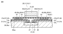
- 4 is a cross-sectional view taken along line IV-IV in FIG. 2 in the embodiment.
- 10A to 10C are diagrams for explaining the reason for providing a slit portion in the metal base board in the embodiment.
- FIG. 4 is an exploded perspective view showing a current path of the coil device in the embodiment.
- FIG. 2 is an exploded perspective view showing an example of a variation of the power conversion device including the coil device in the embodiment.
- FIG. 13 is a cross-sectional view showing an example of a coil device according to a first modified example of the embodiment.
- FIG. 11 is a cross-sectional view showing an example of a coil device according to a second modified example of the embodiment.
- FIG. 13 is a cross-sectional view showing an example of a coil device according to a third modified example of the embodiment.
- 11 is a cross-sectional view showing an example of a power conversion device including a coil device according to a second embodiment.
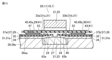
- FIG. FIG. 11 is a cross-sectional view showing a coil device according to an example of a first modified example in the embodiment.
- FIG. 13 is a cross-sectional view showing a coil device according to another example of the first modified example in the embodiment.
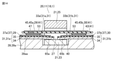
- FIG. 11 is a cross-sectional view showing a coil device according to an example of a second modified example in the embodiment.
- FIG. 13 is a cross-sectional view showing a coil device according to another example of the second modified example in the embodiment.
- 11 is a cross-sectional view showing an example of a power conversion device including a coil device according to a third embodiment.
- FIG. 13 is a cross-sectional view showing an example of a power conversion device including a coil device according to a fourth embodiment.
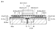
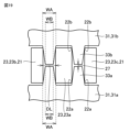
- FIG. 13 is a cross-sectional view showing an example of a coil device according to a modified example of the embodiment. 13 is a partial plan view showing the positional relationship between a core and a metal base substrate in a power conversion device including a coil device according to a fifth embodiment.
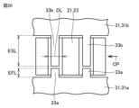
- FIG. 13 is a partial plan view showing the positional relationship between a core and a metal base substrate in a coil device according to a first modified example of the embodiment.
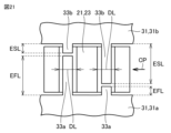
- FIG. 13 is a partial plan view showing the positional relationship between a core and a metal base substrate in a coil device according to a second modified example of the embodiment.
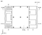
- 13 is a perspective view showing an example of a power conversion device including a coil device according to a sixth embodiment.
- FIG. FIG. 2 is a partial plan view of a power conversion device including a coil device in the embodiment.
- 24 is a partial cross-sectional view taken along line XXIV-XXIV in FIG. 23 in the embodiment.
- FIG. 2 is an enlarged exploded perspective view showing the structure of a coil device in the power conversion device in the embodiment.
- FIG. 13 is a perspective view showing an example of a power conversion device including a coil device according to a modified example in the embodiment.
- FIG. 2 is a partial plan view of a power conversion device including a coil device in the embodiment.
- 28 is a partial cross-sectional view taken along the cross-sectional line XXVIII-XXVIII in FIG. 27 in the embodiment.
- FIG. 1 shows an example of a circuit diagram of a DC-DC converter.
- the DC-DC converter is mounted, for example, on an electric vehicle.
- the DC-DC converter has the function of converting the input voltage of a lithium-ion battery, which is about 100V to 300V, to a voltage of 12V to 15V, and outputting the converted voltage to charge a lead-acid battery.
- the DC-DC converter as a power conversion device 1 includes an inverter circuit section 2, a transformer section 3, a rectifier circuit section 4, a smoothing circuit section 5, an input terminal 6, an input capacitor 8, a control circuit section 10, and an output terminal 7.
- the inverter circuit section 2 is composed of switching elements 9.
- the inverter circuit section 2 is composed of four switching elements: 9a, 9b, 9c, and 9d.
- the switching elements for example, power semiconductor elements such as MOS transistors (MOSFET: Metal Oxide Semiconductor Field Effect Transistors) or insulated gate bipolar transistors (IGBT: Insulated Gate Bipolar Transistors) are used.
- MOSFET Metal Oxide Semiconductor Field Effect Transistors
- IGBT Insulated Gate Bipolar Transistors
- the transformer unit 3 is composed of a transformer 11 having a primary winding portion 11a and a secondary winding portion 11b.
- the rectifier circuit unit 4 is composed of a rectifier element 12.
- the rectifier circuit unit 4 is composed of four rectifier elements 12a, 12b, 12c, and 12d.
- As the rectifier element 12 for example, a power semiconductor element such as a diode, a MOS transistor, or a thyristor is used.
- the smoothing circuit unit 5 is composed of a smoothing reactor 13 and a smoothing capacitor 14.
- the switching operation of each of the four switching elements 9 in the inverter circuit section 2 is controlled by the control circuit section 10, so that the DC voltage input from the input terminal 6 is converted to an AC voltage.
- the AC voltage converted in the inverter circuit section 2 is converted to an arbitrary voltage by the transformer 11.
- the voltage to be converted is determined by the winding ratio of the primary winding section 11a and the secondary winding section 11b in the transformer 11.
- the transformer 11 provides electrical insulation between the input terminal 6 and the output terminal 7.
- the rectifier circuit section 4 the AC voltage supplied from the transformer section 3 is converted back to DC voltage by the rectifier element 12.
- the smoothing circuit section 5 the DC voltage converted by the rectifier circuit section 4 is smoothed by the smoothing reactor 13 and the smoothing capacitor 14. This stabilizes the output voltage output from the output terminal 7.
- the transformer 11 and smoothing reactor 13 are coil devices that generate a relatively large amount of heat. It is necessary to dissipate the heat generated in the transformer 11 and smoothing reactor 13 and lower the temperatures of the transformer 11 and smoothing reactor 13 to an allowable temperature or lower, for example, below approximately 100°C to 120°C. In each embodiment, a structure for dissipating heat from a coil device composed of a coil unit will be specifically described.
- Embodiment 1 a first example of a transformer as a coil device will be described.
- a coil device 20 is composed of one coil unit 18.
- a transformer 11 as the coil device 20 is formed by a core 21 having a loop-shaped magnetic path, and a first winding portion 29 (primary winding portion 11a) and a second winding portion 30 (secondary winding portion 11b) wound around the core 21.
- the first winding portion 29 includes a first coil pattern 37a and a first wiring body 45a.
- the second winding portion 30 includes a second coil pattern 37b and a second wiring body 45b.
- the first coil pattern 37a and the second coil pattern 37b are formed on a metal base substrate 31.
- the first wiring body 45a and the second wiring body 45b are formed on a wiring member 41.
- the first winding portion 29 and the second winding portion 30 are electrically insulated.
- the metal base substrate 31 is placed on a first cooling body 39a as a cooling body 39.
- the transformer 11 includes a metal base substrate 31, wiring member 41, a core 21, and a first cooling body 39a.
- the core 21 is composed of an E-core 23 and an I-core 25.
- the E-core 23 has legs 23a, 23b, and 23c.
- the I-core 25 comes into contact with legs 23a, 23b, and 23c, forming a core 21 with a loop-shaped magnetic path.
- the E-core 23 and the I-core 25 are fixed with an adhesive (not shown).
- the core 21 is, for example, a ferrite core such as a manganese zinc (Mn-Zn) ferrite core or a nickel zinc (Ni-Zn) ferrite core.
- a ferrite core such as a manganese zinc (Mn-Zn) ferrite core or a nickel zinc (Ni-Zn) ferrite core.
- An amorphous core or an iron dust core may also be used as the core 21.
- the core 21 is constructed by combining the E-type core 23 and the I-type core 25, as long as the combination can form a core 21 having a loop-shaped magnetic path, the core is not limited to the E-type core 23 and the I-type core 25.
- the core may be a combination of two U-type cores.
- the core may be a combination of two E-type cores.
- the core may be a combination of a T-type core and a U-type core.
- the metal base substrate 31 is composed of a metal base body 34, an insulating layer 35, and a coil pattern 37.
- the coil pattern 37 is disposed on the metal base body 34 with the insulating layer 35 interposed therebetween.
- the metal base body 34 has a thermal conductivity of 1.0 W/(m ⁇ K) or more, preferably 10.0 W/(m ⁇ K) or more, and more preferably 100.0 W/(m ⁇ K) or more.
- the metal base body 34 is formed from a metal material such as copper, iron, aluminum, an iron alloy, or an aluminum alloy.
- the metal base substrate 31 comprises a first metal base substrate 31a and a second metal base substrate 31b.
- the first metal base substrate 31a includes a first extension portion 33a extending from the outer region of the core 21 to the inner region of the core 21.
- the second metal base substrate 31b includes a second extension portion 33b extending from the outer region of the core 21 to the inner region of the core 21.
- the first metal base substrate 31a and the second metal base substrate 31b are arranged so that the first extension portion 33a and the second extension portion 33b face each other, with an insertion portion 32 formed between the first metal base substrate 31a and the second metal base substrate 31b, through which the legs 23a to 23c of the core 21 are inserted.
- the insertion portion 32 includes an insertion portion 32a through which the leg 23a is inserted, an insertion portion 32b through which the leg 23b is inserted, and an insertion portion 32c through which the leg 23c is inserted.
- the metal base substrate 31 is formed with a slit portion 27 that prevents a loop-shaped induced current from flowing in the portion surrounding the core 21.
- the slit portion 27 is formed in the inner region of the core 21.
- the slit portion 27 is formed in a manner that connects to the insertion portion 32.
- the first extension portion 33a (first metal base substrate 31a) and the second extension portion 33b (second metal base substrate 31b) are disposed with a length SL corresponding to the slit portion 27 between them.
- the slit portion 27 physically and electrically separates the portions of the first metal base substrate 31a and the second metal base substrate 31b that surround the leg portion 23a.
- the slit portion 27 has the function of preventing the formation of a short coil in the metal base body 34. This will be described later.
- the insulating layer 35 has a first main surface 35a and a second main surface 35b.
- the second main surface 35b is in contact with almost the entire surface of the metal base body 33.
- the insulating layer 35 has electrical insulation properties.
- the insulating layer 35 is formed, for example, from epoxy resin, glass fiber reinforced epoxy resin, polyimide resin, or the like. Furthermore, a thermally conductive filler may be mixed into the epoxy resin, etc., to improve thermal conductivity.
- the thickness of the insulating layer 35 is preferably as thin as possible without affecting electrical insulation or manufacturability.
- the thickness of the insulating layer 35 is set, for example, to a thickness of about 1 ⁇ m or more and 2000 ⁇ m or less. More preferably, the thickness of the insulating layer 35 is set to a thickness of about 1 ⁇ m or more and 200 ⁇ m or less.
- the insulating layer 35 is formed with an insertion portion 32a through which the leg 23a of the E-shaped core 23 is inserted, an insertion portion 32b through which the leg 23b is inserted, and an insertion portion 32c through which the leg 23c is inserted.
- a coil pattern 37 is formed on the first main surface 35a of the insulating layer 35.
- the coil pattern 37 includes a first coil pattern 37a and a second coil pattern 37b.
- the first coil pattern 37a is formed on the first metal base substrate 31a.
- the second coil pattern 37b is formed on the second metal base substrate 31b.
- the first coil pattern 37a includes a first coil pattern first part 37af and a first coil pattern second part 37as.
- the inverter circuit part 2 is formed on the first metal base substrate 31a.
- the first coil pattern first part 37af and the first coil pattern second part 37as are electrically connected to the inverter circuit part 2.
- wiring patterns (not shown) other than the first coil pattern 37a may be formed on the first metal base substrate 31a.
- the second coil pattern 37b includes a second coil pattern first part 37bf and a second coil pattern second part 37bs.
- the rectifier circuit part 4 is formed on the second metal base substrate 31b.
- the second coil pattern first part 37bf and the second coil pattern second part 37bs are electrically connected to the rectifier circuit part 4.
- wiring patterns (not shown) other than the second coil pattern 37b may be formed on the second metal base substrate 31b.
- the first metal base substrate 31a on which the first coil pattern 37a and the inverter circuit section 2 are formed has an electrical primary potential.
- the second metal base substrate 31b on which the second coil pattern 37b and the rectifier circuit section 4 are formed has an electrical secondary potential.
- the first metal base substrate 31a having the primary potential and the second metal base substrate 31b having the secondary potential are electrically insulated from each other.
- the thickness of the first coil pattern 37a and the second coil pattern 37b is, for example, about 1 ⁇ m or more and 2000 ⁇ m or less.
- the first coil pattern 37a and the second coil pattern 37b are formed from, for example, copper, nickel, gold, aluminum, silver, tin, or the like.
- the coil pattern 37 may also be formed from an alloy containing these metals.
- Heat generated in the coil pattern 37 is dissipated to the metal base body 34 via the insulating layer 35, which is in contact with almost the entire surface of the metal base body 34.
- the first coil pattern 37a and the metal base body 34 are separated by a creepage distance CR1.
- a creepage distance CR1 When the potential of the first coil pattern 37a and the potential of the metal base body 34 are different, by ensuring the creepage distance CR1, it is possible to prevent dielectric breakdown from occurring on the creepage between the first coil pattern 37a and the metal base body 34.
- the creepage distance CR1 is set based on the potential difference between the potential of the first coil pattern 37a and the potential of the metal base body 34. The larger the potential difference, the longer the creepage distance CR1 needs to be set. From the viewpoint of preventing dielectric breakdown, it is preferable to arrange the first coil pattern 37a in a rounded pattern so as to avoid sharp patterns at corners, etc., whenever possible. In addition, the second coil pattern 37b and the metal base body 34 are separated by a creepage distance CR2. The creepage distance CR2 is also set in the same way as the creepage distance CR1.
- the wiring member 41 is disposed so as to straddle the first metal base substrate 31a and the second metal base substrate 31b which face each other with the slit portion 27 in between.
- the wiring member 41 includes an insulating portion 43 and a wiring body 45.
- the wiring member 41 is formed with an insertion portion 42.
- the insertion portion 42 includes an insertion portion 42a through which the leg portion 23a of the E-shaped core 23 is inserted, an insertion portion 42b through which the leg portion 23b is inserted, and an insertion portion 42c through which the leg portion 23c is inserted.
- a printed wiring board is used as the wiring member 41. In addition to the printed circuit board, for example, a metal bus bar covered with an insulating coating may be used as the wiring member 41.
- the insulating portion 43 has a first main surface 43a and a second main surface 43b.
- the wiring body 45 includes a first wiring body 45a and a second wiring body 45b.
- the first wiring body 45a and the second wiring body 45b are formed from, for example, copper, nickel, gold, aluminum, silver, or tin.
- the first wiring body 45a is formed on the first main surface 43a of the insulating portion 43.
- the first wiring body 45a is disposed so as to surround the insertion portion 42a.
- the second wiring body 45b is formed on the second main surface 43b of the insulating portion 43.
- the second wiring body 45b is disposed so as to surround the insertion portion 42a.
- first wiring body 45a is electrically connected to the first wiring pattern first portion 37af via the through-hole conductive portion 47 and the conductive bonding member 53.
- the other end of the first wiring body 45a is electrically connected to the first wiring pattern second portion 37as via the through-hole conductive portion 47 and the conductive bonding member 53.
- One end of the second wiring body 45b is electrically connected to the second wiring pattern first portion 37bf via the conductive bonding member 53.
- the other end of the second wiring body 45b is electrically connected to the second wiring pattern second portion 37bs via the conductive bonding member 53.
- a conductive adhesive or solder can be used as the joining member 53.
- the first wiring body 45a is thermally joined to the first metal base substrate 31a via the joining member 53 so that the heat can be conducted.
- the second wiring body 45b is thermally joined to the second metal base substrate 31b via the joining member 53 so that the heat can be conducted.
- a heat conductive member (not shown) may be interposed between the wiring body 45 and the coil pattern 37.
- the wiring body 45 and the coil pattern 37 are thermally joined in a manner that allows heat to be conducted through the heat conductive member in addition to the joining member 53.
- the thermal conductivity of the heat conductive member is preferably, for example, 0.1 W/(m ⁇ K) or more, more preferably 1.0 W/(m ⁇ K) or more, and even more preferably 10.0 W/(m ⁇ K) or more.
- heat conductive grease, a heat conductive sheet, or a heat conductive adhesive can be used as the heat conductive member.
- the insulating portion 43 has electrical insulating properties.
- the insulating portion 43 is formed, for example, from glass fiber reinforced epoxy resin, phenolic resin, polyphenylene sulfide (PPS: Poly Phenylene Sulfide), polyether ether ketone (PEEK: Poly Ether Ether Ketone), etc.
- the printed circuit board used as the wiring member 41 may generally be formed from a material that is considered to have a relatively low thermal conductivity.
- the printed circuit board used as the wiring member 41 may be a general-purpose printed circuit board.
- a ceramic substrate such as aluminum oxide, aluminum nitride, or silicon carbide may be used as the printed circuit board used as the wiring member 41.
- a conductive portion (not shown) may be formed on the surface or inside of the wiring member 41.
- the wiring member 41 may be, for example, a laminated bus bar formed by laminating an insulating film sheet and a metal conductor.
- the insulating film sheet may be, for example, a film made of polyethylene terephthalate (PET: Poly Ethylene Terephthalate), a film made of polyimide (PI: Poly Imide), or a paper made of aramid (fully aromatic polyamide) fibers.
- PET Poly Ethylene Terephthalate
- PI Poly Imide
- aramid fully aromatic polyamide
- the metal base substrate 31 on which the coil pattern 37 etc. are formed is placed on the first cooling body 39a.
- the metal base substrate 31 is fixed to the first cooling body 39a by, for example, screws (not shown).
- a groove portion 40 in which the E-shaped core 23 is housed is formed on the main surface 39aa of the first cooling body 39a.
- the thermal conductivity of the first cooling body 39a is preferably, for example, 1.0 W/(m ⁇ K) or more, more preferably 10.0 W/(m ⁇ K) or more, and even more preferably 100.0 W/(m ⁇ K) or more.
- the first cooling body 39a is formed from a metal material such as copper, iron, aluminum, an iron alloy, or an aluminum alloy.
- the first cooling body 39a may also be formed from a resin with high thermal conductivity.
- the first cooling body 39a may be electrically connected to another member so that it has the same potential as the ground potential.
- the metal base substrate 31 is in contact with the main surface 39aa of the first cooling body 39a, so that the first cooling body 39a and the metal base substrate 31 are thermally coupled to each other so that heat can be conducted.
- a thermally conductive member (not shown) between the main surface 39aa of the first cooling body 39a and the metal base substrate 31, heat can be conducted more easily.
- the E-shaped core 23 abuts against the bottom surface of the groove 40 of the first cooling body 39a, so that the core 21 (E-shaped core 23) and the first cooling body 39a are thermally coupled to enable thermal conduction.
- a thermally conductive member (not shown) between the bottom surface of the groove 40 and the E-shaped core 23, heat can be conducted more easily.
- the E-shaped core 23 and the first cooling body 39a may be bonded with an adhesive (not shown) or the like.
- the first cooling body 39a may also be configured to form part of the housing of the coil device 20.
- the first cooling body 39a may also be configured to form part of the housing of the power conversion device 1 including the coil device 20.
- a surface of the first cooling body 39a other than the surface on which the metal base substrate 31 is arranged may be air-cooled or water-cooled.
- the coil device 20 (power conversion device 1) according to the first embodiment is configured as described above.
- the operation of the above-mentioned power conversion device (coil device 20, transformer 11) will be briefly explained.
- the slit portion 27 in the coil device 20 (transformer 11) has the function of preventing the formation of a short coil in the metal base body 34. This will be explained.
- the induced current RP becomes a short coil that is magnetically coupled to the coil pattern 37 in the metal base body 34.
- the coil device 20 transformer 11
- the flow of the induced current RP is blocked, allowing the transformer 11 to exhibit the desired performance.
- the AC voltage converted in the inverter circuit section 2 is converted to an arbitrary voltage by the transformer 11.
- the AC voltage converted by the inverter circuit section 2 flows through a current path PT1.
- the current path PT1 is the first winding section 29 including the first coil pattern 37a and the first wiring body 45a.
- the first winding section 29 becomes the primary winding section 11a in the transformer 11.
- the AC voltage converted to an arbitrary voltage by the transformer 11 flows through the current path PT2.
- the current path PT2 is the second winding section 30 including the second coil pattern 37b and the second wiring body 45b.
- the second winding section 30 becomes the secondary winding section 11b in the transformer 11.
- the AC voltage that flows through the current path PT2 is converted to a DC voltage in the rectifier circuit section 4.
- the AC voltage flows through the primary winding section 11a, causing the primary winding section 11a to generate heat.
- the AC voltage flows through the secondary winding section 11b, causing the secondary winding section 11b to generate heat.
- heat generated in the portion of the first winding portion 29 located in the outer region of the core 21 is dissipated to the first cooling body 39a via the insulating layer 35 and the metal base body 34. Heat generated in the portion of the first winding portion 29 located in the inner region of the core 21 is also dissipated to the first cooling body 39a via the insulating layer 35 and the metal base body 34.
- the heat generated in the portion of the secondary winding portion 11b that is located in the outer region of the core 21 is dissipated to the first cooling body 39a via the insulating layer 35 and the metal base body 34 for the secondary winding portion 11b.
- the heat generated in the portion of the secondary winding portion 11b that is located in the inner region of the core 21 is also dissipated to the first cooling body 39a via the insulating layer 35 and the metal base body 34 for the secondary winding portion 11b.
- heat generated in the portion of the secondary winding portion 11b located in the inner region of the core 21 can be dissipated to the first cooling body 39a to the same extent as heat generated in the portion of the secondary winding portion 11b located in the outer region of the core 21.
- the heat dissipation performance of the coil device 20 can be improved. Also, there is no need to enlarge the first coil pattern 37a and the second coil pattern 37b, etc., for heat dissipation, which contributes to the miniaturization of the coil device 20 and, ultimately, the power conversion device 1.
- the metal base substrate 31 includes a first metal base substrate 31a and a second metal base substrate 31b.
- the first metal base substrate 31a and the second metal base substrate 31b are not an integral metal base substrate, but are separate metal base substrates. Therefore, the area per metal base substrate can be made smaller than when the first metal base substrate 31a and the second metal base substrate 31b are formed from a single integral metal base substrate.
- first metal base substrate 31a and the second metal base substrate 31b are formed as separate metal base substrates, it is possible to standardize the metal base substrate 31 even when the input voltage to the input terminal 6 in the power conversion device 1 is different. This will be explained below.
- the magnetic flux density Bm affects the heat generation of the core 21. For this reason, when the input voltage Vin increases, if the heat dissipation structure of the core 21 is the same, it is preferable that the magnetic flux density Bm is also about the same. Assume that the input voltage Vin input to the input terminal 6 of the power conversion device 1 increases, for example, by three times.
- the period Ton during which the switching element 9 is on is set to 1/3 the original value
- the number of turns N of the first winding portion 29 is set to 3 times the original value
- the cross-sectional area Ae of the leg portion 23a is set to 3 times the original value.
- the period Ton during which the switching element 9 is on is reduced, the amount of heat generated by both the switching element 9 in the inverter circuit section 2 and the rectifier element 12 in the rectifier circuit section 4 will increase. For this reason, if the heat dissipation structure of the switching element 9 and the heat dissipation structure of the rectifier element 12 are the same, it is preferable that the period Ton during which the switching element 9 is on is also the same.
- the metal base substrate 31 may be formed from a single metal base substrate.
- the first metal base substrate 31a and the second metal base substrate 31b need only be spaced apart (length SL) so that the insertion portion 32a (32) through which the leg 23a of the E-type core 23 is inserted is formed without modifying the first metal base substrate 31a and the second metal base substrate 31b.
- the wiring member 41 needs to be modified so that the insertion portion 42a (42) through which the leg 23a of the E-type core 23 is inserted is formed in the wiring member 41.
- the number of turns N of the first winding portion 29 (primary winding portion 11a) in the wiring member 41 has a limited design range that can be selected due to the constraints of the insulation distance and the wiring width. Therefore, by using the first metal base substrate 31a and the second metal base substrate 31b as the metal base substrate 31, it is possible to change the cross-sectional area Ae of the leg portion 23a of the E-shaped core 23, and to expand the design range by combining the number of turns N and the cross-sectional area Ae.
- FIG. 7 shows an example of the structure of the power conversion device 1 (coil device 20) when it is assumed that the input voltage Vin input to the input terminal 6 of the power conversion device 1 is tripled.
- a first metal base substrate 31a and a second metal base substrate 31b are used as the metal base substrate 31, and the insertion portion 42 of the wiring member 41 and the cross-sectional area Ae of the E-shaped core 23 are changed.
- the cross-sectional area Ae (3 ⁇ CD ⁇ CW) of the E-shaped core 23 is three times larger than that of the power conversion device 1 shown in FIG. 2.
- the first metal base substrate 31a and the second metal base substrate 31b are arranged at a distance SL from each other in such a manner that an insertion portion 32 is formed through which the E-shaped core 23, whose cross-sectional area Ae has been three times larger, can be inserted.
- the area of the insertion portion 42 of the wiring member 41 is three times larger.
- the dimensions of the wiring member 41 are changed, and the dimensions of the first metal base board 31a and the second metal base board 31b are not changed, and the first metal base board 31a and the second metal base board 31b before the change are used.
- This makes it possible to standardize the first metal base board 31a and the second metal base board 31b when the electrical specifications are changed. As a result, this contributes to reducing the manufacturing costs of the metal base board 31.
- the first wiring body 45a of the first winding portion 29 is disposed on the first main surface 43a of the insulating portion 43 of the wiring member 41, and the second wiring body 45b of the second winding portion 30 is disposed on the second main surface 43b of the insulating portion 43.
- the voltage of the first winding portion 29 is higher than the voltage of the second winding portion 30
- the current flowing through the second winding portion 30 becomes greater than the current flowing through the first winding portion 29, and the amount of heat generated by the second winding portion 30 becomes greater than the amount of heat generated by the first winding portion 29.
- the second winding section 30 on the second main surface 43b of the insulating section 43, which is closer to the second metal base substrate 31b, and to place the first winding section 29, which has a relatively high voltage, on the first main surface 43a of the insulating section 43 in order to more reliably electrically insulate it.
- the first winding portion 29 and the second winding portion 30 are each wound once around the leg portion 23a of the E-shaped core 23 (one winding (one turn)). Furthermore, a single printed circuit board has been used as an example of the wiring member 41 on which the first wiring body 45a and the second wiring body 45b are arranged.
- the number of turns of each of the first winding portion 29 and the second winding portion 30 may be two or more, depending on the specifications.
- two or more printed circuit boards may be stacked as the wiring member 41.
- one printed circuit board may be electrically connected to the other printed circuit boards by a conductive joining member.
- a multilayer printed circuit board in which wiring bodies and insulating parts are alternately stacked may be used.
- a coil device 20 (power conversion device 1) according to a first modified example will be described.
- a sealing member 55 is filled between the metal base substrate 31 and the wiring member 41.
- a sealing member 55 is filled between the core 21 (E-shaped core 23) and the first cooling body 39a (groove portion 40). Note that the rest of the configuration is similar to that of the coil device 20 shown in Fig. 4, so the same members are given the same reference numerals and the description thereof will not be repeated unless necessary.
- the sealing member 55 is preferably formed from a material having a thermal conductivity of about 0.1 W/(m ⁇ K) or more, preferably about 1.0 W/(m ⁇ K).
- the sealing member 55 is electrically insulating.
- the sealing member 55 may have a Young's modulus of 1 MPa or more.
- the sealing member 55 may be formed from a resin material having elasticity.
- the sealing member 55 may be formed from an epoxy resin containing a thermally conductive filler.
- the sealing member 55 may be formed from a rubber material such as silicone or urethane.
- the heat generated in the metal base substrate 31 and the heat generated in the wiring member 41 can be dissipated to the first cooling body 39a via the sealing member 55.
- a sealing member 55 is filled between the metal base substrate 31 and the wiring member 41, including between the first metal base substrate 31a and the second metal base substrate 31b. This makes it possible to prevent the surface of the metal base substrate 31 from being contaminated by electrically conductive substances. As a result, it is possible to reduce both the creepage distance between the first coil pattern 37a and the metal base body 34 and the creepage distance between the second coil pattern 37b and the metal base body 34, which contributes to the miniaturization of the coil device 20 and, ultimately, the miniaturization of the power conversion device 1.
- a sealing member 55 is filled between the groove 40 and the E-shaped core 23. This allows heat generated in the core 21 to be dissipated to the first cooling body 39a via the sealing member 55. As a result, there is no need to enlarge the core 21 for heat dissipation, which further contributes to the miniaturization of the coil device 20 and, ultimately, the power conversion device 1.
- the sealing member 55 fixes the wiring member 41 to the metal base substrate 31, and fixes the core 21 (E-shaped core 23) to the first cooling body 39a.
- the vibration resistance of the coil device 20, and therefore the vibration resistance of the power conversion device 1 can be improved.
- a coil device 20 (power conversion device 1) according to a second modification will be described.
- an elastic member 57 such as a spring as a biasing member is interposed between the metal base substrate 31 and the E-shaped core 23. Note that other configurations are similar to those of the coil device 20 shown in Fig. 4, so the same members are given the same reference numerals and the description thereof will not be repeated unless necessary.
- an elastic member 57 is interposed between the metal base substrate 31 and the E-shaped core 23.
- heat generated in the E-shaped core 23 (core 21) is efficiently conducted to the metal base substrate 31 (first metal base substrate 31a and second metal base substrate 31b) via the elastic member 57 such as a spring, and the heat conducted to the metal base substrate 31 (metal base main body 34) is dissipated to the first cooling body 39a.
- the elastic member 57 such as a spring
- the elastic member 57 interposed between the metal base substrate 31 and the E-core 23 biases the E-core 23 (core 21) against the first cooling body 39a.
- the vibration resistance of the coil device 20, and therefore the vibration resistance of the power conversion device 1 can be improved.
- a coil device 20 (power conversion device 1) according to a third modified example will be described.
- a metal base substrate 31 is formed with an uneven portion 59 as a biasing member.
- the uneven portion 59 is interposed between the metal base substrate 31 and the E-shaped core 23. Burrs generated when processing the metal base substrate 31 are used as the uneven portion 59.
- Press processing is an example of the outer shape processing of the metal base substrate 31 (metal base main body 34).
- a die In press processing, a die is used to apply pressure to the metal base substrate 31 (metal base body 34), thereby processing the metal base substrate 31.
- burrs are generated on the metal base body 34. The burrs are generated so that they protrude from the surface of the metal base substrate 31. For example, the burrs are generated so that convex portions and concave portions are alternately connected.
- burrs generated by the press process are used as uneven portions 59 and are interposed between the metal base substrate 31 and the E-shaped core 23 (core 21). Note that the rest of the configuration is the same as that of the coil device 20 shown in Figure 4, so the same members are given the same reference numerals and their descriptions will not be repeated unless necessary.
- burrs generated on the metal base substrate 31 during press processing are interposed between the metal base substrate 31 and the E-shaped core 23 as uneven portions 59. Therefore, the E-shaped core 23 (core 21) is biased against the first cooling body 39a by the uneven portions 59 interposed between the metal base substrate 31 and the E-shaped core 23.
- the convex portions of the uneven portion 59 acting as burrs have a pointed shape. This restricts the movement of the E-shaped core 23 (21) in a direction intersecting the direction in which the E-shaped core 23 (core 21) is urged toward the first cooling body 39a. As a result, the vibration resistance of the coil device 20, and therefore the vibration resistance of the power conversion device 1, can be further improved.
- the uneven portion 59 biases the E-shaped core 23 (core 21) against the first cooling body 39a, so that heat generated in the core 21 can be efficiently dissipated to the first cooling body 39a.
- the core 21 for heat dissipation, which further contributes to the miniaturization of the coil device 20 and, ultimately, the power conversion device 1.
- Embodiment 2 a second example of a transformer as a coil device will be described.
- a metal base substrate 31 is formed with step portions 61a and 61b as sandwiching portions for sandwiching an E-shaped core 23 (core 21).
- the first extension portion 33a of the first metal base substrate 31a and the second extension portion 33b of the second metal base substrate 31b face each other with the slit portion 27 in between.
- the step portion 61a is formed in the first extension portion 33a of the first extension portion 33a and the second extension portion 33b that face each other.
- the step portion 61b is formed in the second extension portion 33b of the first extension portion 33a and the second extension portion 33b that face each other.
- One end of the E-shaped core 23 is received in the step portion 61a, and the other end of the E-shaped core 23 is received in the step portion 61b, so that the E-shaped core 23 is sandwiched between the step portion 61a (first extension portion 33a) and the step portion 61b (second extension portion 33b) and is biased against the first cooling body 39a.
- the rest of the configuration is similar to that of the coil device 20 shown in Figure 4, so the same members are given the same reference numerals and the description will not be repeated unless necessary.
- the E-shaped core 23 is sandwiched between the step portion 61a in the first extension portion 33a and the step portion 61b in the second extension portion 33b, and is biased against the first cooling body 39a. This restricts the movement of the E-shaped core 23. As a result, the vibration resistance of the coil device 20, and therefore the vibration resistance of the power conversion device 1, can be improved.
- the contact area between the E-shaped core 23 and the first metal base substrate 31a increases. Since the E-shaped core 23 is received in the step portion 61b, the contact area between the E-shaped core 23 and the second metal base substrate 31b (second extension portion 33b) increases.
- the heat generated in the E-shaped core 23 (core 21) is efficiently conducted to the metal base substrate 31 (first metal base substrate 31a and second metal base substrate 31b), and the heat conducted to the metal base substrate 31 (metal base main body 34) is dissipated to the first cooling body 39a.
- the core 21 for heat dissipation there is no need to enlarge the core 21 for heat dissipation, which can further contribute to the miniaturization of the coil device 20 and, ultimately, the power conversion device 1.
- a coil device 20 (power conversion device 1) according to a first modified example will be described.
- a cambered portion 63a that is cambered upward from the E-core 23 toward the wiring member 41 is formed on a first extension portion 33a of a first metal base substrate 31a.
- a cambered portion 63b that is cambered upward from the E-core 23 toward the wiring member 41 is formed on a second extension portion 33b of a second metal base substrate 31b.
- the thickness of the E-shaped core 23 is set to a thickness equal to or greater than the depth of the groove 40, and the upwardly curved portions 63a and 63b are configured to abut against the E-shaped core 23. Note that the rest of the configuration is similar to that of the coil device 20 shown in Figure 4, so the same members are given the same reference numerals and descriptions thereof will not be repeated unless necessary.
- the E-shaped core 23 is sandwiched between the first metal base substrate 31a (upwardly curved portion 63a) and the first cooling body 39a, and the E-shaped core 23 is sandwiched between the second metal base substrate 31b (upwardly curved portion 63b) and the first cooling body 39a.
- the E-shaped core 23 is urged toward the first cooling body 39a by the upwardly curved portions 63a and 63b, and the E-shaped core 23 (core 21) is fixed to the first cooling body 39a.
- the E-core 23 is biased against the first cooling body 39a by the upward cambered portions 63a and 63b, thereby improving the vibration resistance of the coil device 20 and, ultimately, the vibration resistance of the power conversion device 1. Furthermore, the E-core 23 is biased against the first cooling body 39a by the upward cambered portions 63a and 63b, thereby enabling heat generated in the E-core 23 (core 21) to be efficiently dissipated to the first cooling body 39a.
- a sloping portion 24 may be provided along each of the upward cambered portion 63a and the upward cambered portion 63b in the portion of the E-shaped core 23 where the upward cambered portion 63a and the upward cambered portion 63b contact each other.
- a coil device 20 (power conversion device 1) according to a second modified example will be described.
- a downwardly curved portion 65a that curves downward from the first cooling body 39a toward the E-core 23 is formed on the first extension portion 33a of the first metal base substrate 31a.
- a downwardly curved portion 65b that curves downward from the first cooling body 39a toward the E-core 23 is formed on the second extension portion 33b of the second metal base substrate 31b.
- the thickness of the E-shaped core 23 is set to a thickness equal to or less than the thickness corresponding to the depth of the groove portion 40, and the downwardly curved portion 65a and the downwardly curved portion 65b are configured to abut against the E-shaped core 23. Note that the rest of the configuration is similar to that of the coil device 20 shown in Figure 4, so the same members are given the same reference numerals and the description will not be repeated unless necessary.
- the E-shaped core 23 is sandwiched between the first metal base substrate 31a (downwardly curved portion 65a) and the first cooling body 39a, and the E-shaped core 23 is sandwiched between the second metal base substrate 31b (downwardly curved portion 65b) and the first cooling body 39a.
- the E-shaped core 23 is urged toward the first cooling body 39a by the downwardly curved portions 65a and 65b, and the E-shaped core 23 (core 21) is fixed to the first cooling body 39a.
- the downward curvature 65a and the downward curvature 65b bias the E-core 23 against the first cooling body 39a, thereby improving the vibration resistance of the coil device 20 and, ultimately, the vibration resistance of the power conversion device 1. Furthermore, the downward curvature 65a and the downward curvature 65b bias the E-core 23 against the first cooling body 39a, thereby allowing the heat generated in the E-core 23 (core 21) to be efficiently dissipated to the first cooling body 39a.
- a sloping portion 24 may be provided along the downwardly curved portion 65a and the downwardly curved portion 65b at the portion of the E-shaped core 23 where the downwardly curved portion 65a and the downwardly curved portion 65b contact each other.
- Embodiment 3 a third example of a transformer as a coil device will be described.
- a convex portion 67 protruding toward the slit portion 27 is formed on the E-shaped core 23.
- the convex portion 67 is sandwiched between the first extension portion 33a (first metal base substrate 31a) and the second extension portion 33b (second metal base substrate 31b).
- the other configurations are the same as those of the coil device 20 shown in Fig. 4, so the same members are denoted by the same reference numerals, and the description thereof will not be repeated unless necessary.
- the E-shaped core 23 is formed with a convex portion 67 that protrudes toward the slit portion 27. This allows the E-shaped core 23 to be pressed against the first cooling body 39a with the core 21 (E-shaped core 23) sandwiched between the first metal base substrate 31a and the second metal base substrate 31b. This improves the vibration resistance of the coil device 20, and ultimately the vibration resistance of the power conversion device 1.
- the convex portion 67 on the E-shaped core 23 is sandwiched between the first metal base substrate 31a and the second metal base substrate 31b, thereby increasing the contact area between the E-shaped core 23 and each of the first metal base substrate 31a and the second metal base substrate 31b.
- Embodiment 4 a fourth example of a transformer as a coil device will be described.
- a screw member 69 is attached as a first fixing member, penetrating the first extension portion 33a (first metal base substrate 31a) and the E-shaped core 23 to reach the first cooling body 39a.
- a screw member 69 is attached as a first fixing member, penetrating the second extension portion 33b (second metal base substrate 31b) and the E-shaped core 23 to reach the first cooling body 39a.
- the rest of the configuration is similar to that of the coil device 20 shown in Fig. 4, so the same members are given the same reference numerals, and the description thereof will not be repeated unless necessary.
- the first metal base substrate 31a, the second metal base substrate 31b, and the E-shaped core 23 are fixed to the first cooling body 39a by the screw members 69. This improves the vibration resistance of the coil device 20, and therefore the vibration resistance of the power conversion device 1.
- a coil device 20 (power conversion device) according to a modified example will be described.
- an insulating member 71 is filled between the first metal base substrate 31a (first extension portion 33a) and the second metal base substrate 31b (second extension portion 33b).
- a screw member 73 is attached as a second fixing member, penetrating the insulating member 71 and the E-shaped core 23 and reaching the first cooling body 39a. Note that the other configurations are the same as those of the coil device 20 shown in Fig. 4, so the same members are given the same reference numerals, and the description thereof will not be repeated unless necessary.
- the insulating member 71 and the E-shaped core 23 interposed between the first extension portion 33a and the second extension portion 33b are fixed to the first cooling body 39a by the screw member 73. This improves the vibration resistance of the coil device 20, and therefore the vibration resistance of the power conversion device 1.
- the heat generated in the core 21 can be efficiently dissipated to the first cooling body 39a.
- the insulating member 71 may be made of any material that is electrically insulating. This makes it possible to more effectively prevent dielectric breakdown in the region between the first metal base substrate 31a and the second metal base substrate 31b.
- Embodiment 5 a fifth example of a transformer as a coil device will be described.
- the first extension 33a first metal base substrate 31a
- the second extension 33b second metal base substrate 31b
- the rest of the configuration is similar to that of the coil device 20 shown in Fig. 4, so the same members are given the same reference numerals and the description thereof will not be repeated unless necessary.
- the portions (root portions) of the first extension portion 33a and the second extension portion 33b that are located in the outer region of the core 21 have a width WA.
- the tip portions (inner region of the core 21) of the first extension portion 33a and the second extension portion 33b have a width WB.
- the distance between adjacent leg portions 23a and 23b (or leg portions 23c) is distance DL.
- Width WA is set wider than distance DL.
- Width WB is set narrower than distance DL.
- one first extension portion 33a abuts against the corners 22a of both legs 23a and 23b.
- the other first extension portion 33a abuts against the corners 22a of both legs 23a and 23c.
- one second extension portion 33b abuts against the corners 22b of both legs 23a and 23b.
- the other second extension portion 33b abuts against the corners 22b of both legs 23a and 23c.
- the first extension 33a abuts against the corner 22a of the E-core 23, and the second extension 33b abuts against the corner 22b of the E-core, so that the core 21 (E-core 23) is sandwiched between the first extension 33a and the second extension 33b.
- the vibration resistance of the coil device 20, and therefore the vibration resistance of the power conversion device 1 can be improved.
- the first extension portion 33a has a length EFL from the outer region to the inner region of the core 21.
- the second extension portion 33b has a length ESL from the outer region to the inner region of the core 21.
- the length EFL of each of the two first extension portions 33a is shorter than the length ESL of each of the two second extension portions 33b.
- the two second extension portions 33b each having the length ESL are located in the inner region of the core 21 beyond the center portion CP (extension direction) of the core 21.
- the two second extensions 33b in the second metal base substrate 31b are positioned beyond the central portion CP of the core 21.
- heat generated near the central portion CP where the amount of heat generated in the core 21 is the highest, is efficiently conducted to the second metal base substrate 31b via the two second extensions 33b.
- the heat conducted to the second metal base substrate 31b is dissipated to the first cooling body 39a.
- the two first extensions 33a of the first metal base substrate 31a may be positioned beyond the central portion CP of the core 21. In this case, heat generated near the central portion CP, where the amount of heat generated in the core 21 is the highest, is efficiently conducted to the first metal base substrate 31a via the two first extensions 33a. The heat conducted to the first metal base substrate 31a is dissipated to the first cooling body 39a.
- the first extension 33a has a length EFL from the outer region to the inner region of the core 21.
- the second extension 33b has a length ESL from the outer region to the inner region of the core 21.
- the length EFL of one of the first extensions 33a is longer than the length ESL of one of the second extensions 33b.
- the length EFL of the other first extension 33a is shorter than the length ESL of the other second extension 33b.
- One of the first extensions 33a having the length EFL is located in the inner region of the core 21 beyond the center CP (extension direction) of the core 21.
- the other of the second extensions 33b having the length ESL is located in the inner region of the core 21 beyond the center CP (extension direction) of the core 21.
- one of the first extensions 33a in the first metal base substrate 31a is positioned beyond the central portion CP of the core 21.
- the other of the second extensions 33b in the second metal base substrate 31b is positioned beyond the central portion CP of the core 21.
- heat generated near the central portion CP where the amount of heat generated in the core 21 is the highest, is efficiently conducted to the first metal base substrate 31a via one of the first extensions 33a, and is also efficiently conducted to the second metal base substrate 31b via the other of the second extensions 33b.
- the heat conducted to the first metal base substrate 31a and the second metal base substrate 31b is dissipated to the first cooling body 39a.
- Embodiment 6 a sixth example of a transformer as a coil device will be described.
- the description will be given using an XYZ orthogonal coordinate system as necessary.
- the same members as those in the configuration of the coil device 20 shown in FIG. 4 and the like are given the same reference numerals, and the description will not be repeated unless necessary.
- the transformer 11 as the coil device 20 includes the first core 21a, the second core 21b, the third core 21c and the fourth core 21d as the cores 21.
- the cooling bodies 39 in addition to the first cooling body 39a, the second cooling body 39b, the third cooling body 39c, the fourth cooling body 39d, the fifth cooling body 39e and the sixth cooling body 39f are included.
- Each of the second cooling body 39b, the third cooling body 39c, the fourth cooling body 39d, the fifth cooling body 39e and the sixth cooling body 39f is placed on the first cooling body 39a.
- the second cooling body 39b to the sixth cooling body 39f are thermally joined to the first cooling body 39a.
- the first wiring body 45a includes a first wiring body first part 45aa and a first wiring body second part 45ab. Each of the first wiring body first part 45aa and the first wiring body second part 45ab includes a part extending along the X-axis as the first direction.
- the second wiring body 45b includes a second wiring body first part 45ba and a second wiring body second part 45bb. Each of the second wiring body first part 45ba and the second wiring body second part 45bb includes a part extending along the X-axis.
- the first wiring body first part 45aa and the second wiring body first part 45ba, and the first wiring body second part 45ab and the second wiring body second part 45bb are arranged at a distance in the Y-axis direction as the second direction.
- the second core 21b is arranged at a distance from the first core 21a in the X-axis direction.
- the third core 21c is arranged at a distance from the first core 21a in the Y-axis direction.
- the fourth core 21d is arranged at a distance from the third core 21c in the X-axis direction, and at a distance from the second core 21b in the Y-axis direction.
- the four cores, the first core 21a to the fourth core 21d, are arranged in a matrix (2x2).
- the second cooling body 39b is disposed between the first core 21a and the second core 21b.
- the second cooling body 39b is disposed with a gap between it and the first core 21a and the second core 21b.
- the third cooling body 39c is disposed between the first core 21a and the third core 21c, and is also disposed between the second core 21b and the fourth core 21d.
- the fourth cooling body 39d is arranged on the side opposite the first core 21a from the side on which the third cooling body 39c is arranged, with the first core 21a sandwiched between the fourth cooling body 39d and the third cooling body 39c.
- the fourth cooling body 39d is arranged on the side opposite the second core 21b from the side on which the third cooling body 39c is arranged, with the second core 21b sandwiched between the fourth cooling body 39d and the third cooling body 39c.
- the fifth cooling body 39e is arranged on the side opposite the third core 21c from the side on which the third cooling body 39c is arranged, with the third core 21c sandwiched between the fifth cooling body 39e and the third cooling body 39c.
- the fifth cooling body 39e is arranged on the side opposite the fourth core 21d from the side on which the third cooling body 39c is arranged, with the fourth core 21d sandwiched between the fifth cooling body 39e and the third cooling body 39c.
- the sixth cooling body 39f is arranged between the third cooling body 39c and the fourth cooling body 39d.
- the sixth cooling body 39f is arranged with a gap between it and each of the third cooling body 39c and the fourth cooling body 39d.
- the third cooling body 39c is in contact with each of the first core 21a, the second core 21b, the third core 21c, and the fourth core 21d.
- the third cooling body 39c is thermally bonded to each of the first core 21a, the second core 21b, the third core 21c, and the fourth core 21d.
- the fourth cooling body 39d is in contact with each of the first core 21a and the second core 21b.
- the fourth cooling body 39d is thermally bonded to each of the first core 21a and the second core 21b.
- the fifth cooling body 39e is in contact with each of the third core 21c and the fourth core 21d.
- the fifth cooling body 39e is thermally bonded to each of the third core 21c and the fourth core 21d.
- the core 21 (first core 21a to fourth core 21d) is thermally bonded to the first cooling body 39a via each of the third cooling body 39c, the fourth cooling body 39d, and the fifth cooling body 39e.
- Each of the second cooling body 39b and the sixth cooling body 39f includes an E-type cooling body 38a as the first part of the second cooling body, and an I-type cooling body 38b as the second part of the second cooling body.
- the E-type cooling body 38a is disposed in the first cooling body 39a.
- the I-type cooling body 38b is disposed so as to face the E-type cooling body 38a.
- the E-type cooling body 38a has legs 38aa, 38ab, and 38ac.
- the I-type cooling body 38b is disposed so as to be in contact with each of the legs 38aa, 38ab, and 38ac.
- the E-type cooling body 38a and the I-type cooling body 38b are arranged so as to sandwich the wiring member 41 from the side where the first cooling body 39a is arranged and the side opposite to the side where the first cooling body 39a is arranged.
- the E-type cooling body 38a is thermally joined to the wiring member 41 via a heat conductive member 75.
- the I-type cooling body 38b is thermally joined to the wiring member 41 via a heat conductive member 76.
- the wiring member 41 is thermally joined to the first cooling body 39a via each of the second cooling body 39b and the sixth cooling body 39f.
- the second cooling body 39b and the sixth cooling body 39f are configured by combining the E-type cooling body 38a and the I-type cooling body 38b, but as long as the wiring member 41 can be sandwiched by combining them, the configuration is not limited to the E-type cooling body 38a and the I-type cooling body 38b. For example, a configuration in which two E-type cooling bodies are combined may also be used.
- each of the second cooling body 39b to the sixth cooling body 39f is preferably 1.0 W/(m ⁇ K) or more, more preferably 10.0 W/(m ⁇ K) or more, and even more preferably 100.0 W/(m ⁇ K) or more.
- Each of the second cooling body 39b to the sixth cooling body 39f is formed from a metal material such as copper, iron, aluminum, an iron alloy, or an aluminum alloy.
- each of the second cooling body 39b to the sixth cooling body 39f may be formed, for example, from a resin having high thermal conductivity.
- Each of the second cooling body 39b to the sixth cooling body 39f may be electrically connected to another member so that it has the same potential as the ground potential.
- the wiring member 41 has the following insertion portions 42: insertion portion 42a, insertion portion 42b, insertion portion 42c, insertion portion 42d, and insertion portion 42e.
- the leg 23c (see FIG. 2) of the core 21 (first core 21a and second core 21b), the leg 23b (see FIG. 2) of the core 21 (third core 21c and fourth core 21d), the third cooling body 39c, the leg 38ac of the E-type cooling body 38a (second cooling body 39b), and the leg 38ab of the E-type cooling body 38a (sixth cooling body 39f) are inserted into the insertion portion 42a.
- the legs 23a (see FIG. 2) of the core 21 (first core 21a and second core 21b) and the legs 38aa of the E-type cooling body 38a (second cooling body 39b) are inserted into the insertion portion 42b.
- the legs 23a (see FIG. 2) of the core 21 (third core 21c and fourth core 21d) and the legs 38aa of the E-type cooling body 38a (sixth cooling body 39f) are inserted into the insertion portion 42c.
- the leg 23b (see FIG. 2) of the core 21 (first core 21a and second core 21b), the leg 38ab of the E-type cooling body 38a (second cooling body 39b), and the fourth cooling body 39d are inserted into the insertion portion 42d.
- the leg 23c (see FIG. 2) of the core 21 (third core 21c and fourth core 21d), the leg 38ac of the E-type cooling body 38a (sixth cooling body 39f), and the fifth cooling body 39e are inserted into the insertion portion 42e.
- the first wiring body first part 45aa and the second wiring body first part 45ba are wound around the first core 21a and the second core 21b with the second cooling body 39b interposed between the first core 21a and the second core 21b.
- the first wiring body second part 45ab and the second wiring body second part 45bb are wound around the third core 21c and the fourth core 21d with the sixth cooling body 39f interposed between the third core 21c and the fourth core 21d.
- the second cooling body 39b and the sixth cooling body 39f are each thermally joined to the wiring member 41 via the thermal conductive member 75 or the thermal conductive member 76. This allows heat generated in the wiring member 41 to be dissipated to the first cooling body 39a via the second cooling body 39b and the sixth cooling body 39f. As a result, there is no need to increase the size of the wiring member 41 for heat dissipation, which contributes to the miniaturization of the coil device 20 and, ultimately, the miniaturization of the power conversion device 1.
- the third cooling body 39c is thermally bonded to each of the first core 21a, the second core 21b, the third core 21c, and the fourth core 21d.
- the fourth cooling body 39d is thermally bonded to each of the first core 21a and the second core 21b.
- the fifth cooling body 39e is thermally bonded to each of the third core 21c and the fourth core 21d.
- the core 21 is arranged with a gap between it and the second cooling body 39b and the sixth cooling body 39f, but the core 21 may be arranged so as to be in contact with the second cooling body 39b and the sixth cooling body 39f. That is, the first core 21a and the second core 21b may be arranged so as to be in contact with the second cooling body 39b, and the third core 21c and the fourth core 21d may be arranged so as to be in contact with the sixth cooling body 39f.
- the heat generated in the core 21 can be conducted to each of the second cooling body 39b and the sixth cooling body 39f and dissipated to the first cooling body 39a, and the heat generated in the core 21 can be effectively dissipated to the first cooling body 39a.
- there is no need to enlarge the core 21 for heat dissipation which can further contribute to the miniaturization of the coil device 20 and, ultimately, the power conversion device 1.
- the coil device 20 includes a lid cooling body 39g in addition to the first cooling body 39a to the sixth cooling body 39f as the cooling body 39.
- the lid cooling body 39g is disposed so as to cover the core 21 (the first core 21a to the fourth core 21d) and the second cooling body 39b to the sixth cooling body 39f.
- a heat conductive member 77 is interposed between the lid cooling body 39g and the core 21 and the second cooling body 39b to the sixth cooling body 39f.
- the lid cooling body 39g is fixed to the second cooling body 39b to the sixth cooling body 39f by screw members 74. Note that the rest of the configuration is similar to that of the coil device 20 shown in Figures 22 to 24 or Figure 4, etc., so the same members are given the same reference numerals and their descriptions will not be repeated unless necessary.
- the thermal conductivity of the lid cooling body 39g is preferably 1.0 W/(m ⁇ K) or more, more preferably 10.0 W/(m ⁇ K) or more, and even more preferably 100.0 W/(m ⁇ K) or more.
- the lid cooling body 39g is formed from a metal material such as copper, iron, aluminum, an iron alloy, or an aluminum alloy.
- the lid cooling body 39g may be formed, for example, from a resin having high thermal conductivity.
- the lid cooling body 39g may be electrically connected to another member so that it has the same potential as the ground potential.
- a thermally conductive member 77 is interposed between the lid cooling body 39g and the core 21 and the second cooling body 39b to the sixth cooling body 39f.
- the lid cooling body 39g is thermally bonded to the core 21 and the second cooling body 39b to the sixth cooling body 39f via the thermally conductive member 77.
- the second cooling body 39b to the sixth cooling body 39f are thermally bonded to the first cooling body 39a.
- the core 21 and the second cooling body 39b to the sixth cooling body 39f, together with the lid cooling body 39g, are fixed to the first cooling body 39a by the screw member 74. This improves the vibration resistance of the coil device 20, and therefore the vibration resistance of the power conversion device 1.
- the core 21 is described as having four cores, the first core 21a to the fourth core 21d, arranged in a matrix (2 x 2).
- the number and arrangement of the cores 21 are not limited to this.
- the coil device described in each of the above-mentioned embodiments is described as being composed of one coil unit, the coil device can also be applied to a coil device composed of two or more coil units.
- the coil device 20 (power conversion device 1) described in each embodiment can be combined in various ways as needed.
- a coil device having a coil unit includes: One or more cores having a looped magnetic path; a metal base substrate disposed in an inner region of the core and an outer region of the core, the metal base substrate having a first coil pattern and a second coil pattern formed on a metal base body with an insulating layer interposed therebetween; a first winding portion including the first coil pattern and wound around the core in a manner passing through the inner region of the core; a second winding portion including the second coil pattern, wound around the core in a manner passing through the inner region of the core, and electrically insulated from the first winding portion; one or more cooling bodies including a first cooling body joined to the metal base body on the side opposite to the side on which the insulating layer is formed;
- the metal base substrate is a first metal base substrate on which the first coil pattern is formed; a second metal base substrate on which the second coil pattern is formed, A coil device in which the first metal base substrate and the second metal base substrate are
- a slit portion for preventing a loop-shaped induced current from flowing in a portion surrounding the core is formed in the metal base substrate in a manner connected to the insertion portion; 2.
- the first coil pattern is A first coil pattern first portion; a first coil pattern second portion;
- the second coil pattern is A first portion of a second coil pattern; a second coil pattern second portion;
- the wiring body is a first wiring body electrically connecting the first coil pattern first portion and the first coil pattern second portion; a second wiring main body electrically connecting the second coil pattern first portion and the second coil pattern second portion, the first winding portion includes the first wiring main body, 3.
- the wiring member is a printed circuit board, 4.
- the wiring member is disposed on an opposite side of the metal base substrate from a side where the first cooling body is disposed, in an aspect of being located in the inner region of the core and the outer region of the core surrounded by the core,
- the first cooling body is formed with a receiving groove portion for receiving the core, 5.
- Appendix 6 A coil device described in any one of appendix 1 to 5, wherein a biasing member is interposed between the metal base substrate and the core, biasing a portion of the core located between the metal base substrate and the first cooling body toward the first cooling body.
- the first metal base substrate includes a first extension portion extending from the outer region of the core to the inner region of the core; the second metal base substrate includes a second extension portion extending from the outer region of the core to the inner region of the core; A coil device described in any one of appendix 1 to 6, wherein the first metal base substrate and the second metal base substrate are arranged so that the first extension portion and the second extension portion face each other.
- Appendix 8 A coil device as described in Appendix 7, wherein the first extension portion and the second extension portion are formed with a clamping portion that clamps a portion of the core located between the metal base substrate and the first cooling body between the first extension portion and the second extension portion.
- Appendix 9 A coil device as described in Appendix 7, wherein the first extension portion and the second extension portion are formed with a warped portion that sandwiches a portion of the core located between the metal base substrate and the first cooling body between the metal base substrate and the first cooling body and urges the portion toward the first cooling body.
- Appendix 10 A coil device as described in Appendix 7, wherein the core is formed with a protrusion protruding from a portion of the core located between the metal base substrate and the first cooling body toward between the first extension portion and the second extension portion.
- the core is a first leg around which the first winding portion and the second winding portion are wound; a second leg portion positioned at a first distance from the first leg portion, the first extension portion and the second extension portion are located between the first leg portion and the second leg portion so as to face each other,
- the first extension portion is formed so that a width thereof narrows from a first width wider than the first interval to a second width narrower than the first interval toward a tip of the first extension portion
- the second extension portion is formed so that a width thereof narrows from a third width wider than the first interval to a fourth width narrower than the first interval toward a tip of the second extension portion,
- the coil device of claim 7, wherein the metal base substrate is arranged to sandwich the core with the first extension portion abutting against the first leg portion and the second leg portion and the second extension portion abutting against the first leg portion and the second leg portion.
- Appendix 12 A coil device as described in Appendix 7, wherein a first fixing member is attached from each of the first extension portion and the second extension portion, passing through a portion of the core located between the metal base substrate and the first cooling body and reaching the first cooling body.
- An insulating member is filled between the first extension portion and the second extension portion, 8.
- the first extension portion has a first extension length extending from the outer region of the core to the inner region of the core; the second extension portion has a second extension length extending from the outer region of the core to the inner region of the core; 8. The coil device according to claim 7, wherein the first extension length is set to either a first length longer than the second extension length or a second length shorter than the second extension length.
- the core includes a first core and a second core arranged at a distance from each other in a first direction, the cooling body includes a second cooling body disposed between the first core and the second core and thermally joined to the first cooling body;
- the coil device according to any one of appendices 3 to 5, wherein the first wiring body and the second wiring body are wound around the first core and the second core, respectively, with the second cooling body interposed between the first core and the second core.
- the second cooling body is A second cooling body first part disposed on the first cooling body; a second cooling body second part disposed to face the second cooling body first part, The coil device of claim 15, wherein the second cooling body first part and the second cooling body second part are arranged to sandwich the wiring member from the side where the first cooling body is arranged and the side opposite to the side where the first cooling body is arranged.
- Appendix 18 The coil device according to any one of appendixes 15 to 17, wherein the second cooling body is arranged so as to be in contact with each of the first core and the second core.
- the first wiring main body includes a first wiring main body first part and a first wiring main body second part connected in series
- the second wiring main body includes a second wiring main body first part and a second wiring main body second part connected in series, each of the first wiring body first portion, the first wiring body second portion, the second wiring body first portion, and the second wiring body second portion includes a portion extending in a first direction; the first wiring body first portion and the first wiring body second portion, and the second wiring body first portion and the second wiring body second portion are disposed at a distance from each other in a second direction intersecting the first direction
- the cores include a first core and a third core that are spaced apart from each other in the second direction
- the cooling body includes a third cooling body, a fourth cooling body, and a fifth cooling body, each of which is thermally joined to the first cooling body; the third cooling body is disposed between the first core and the third core in a manner in which the third cooling body is in contact with each of the first core and the third core; the fourth cooling cooling
- the first wiring main body includes a first wiring main body first part and a first wiring main body second part connected in series
- the second wiring main body includes a second wiring main body first part and a second wiring main body second part connected in series
- each of the first wiring body first portion, the first wiring body second portion, the second wiring body first portion, and the second wiring body second portion includes a portion extending in a first direction
- the first wiring body first portion and the first wiring body second portion, and the second wiring body first portion and the second wiring body second portion are disposed at a distance from each other in a second direction intersecting the first direction
- the core is A first core; a second core disposed at a distance from the first core in the first direction; a third core disposed at a distance from the first core in the second direction; a fourth core disposed at a distance from the third core in the first direction and at a distance from the second core in the second direction, the first wiring main body first portion and the second wiring main body first portion are wound around the first core and the second core, respectively
- the cooling bodies include a second cooling body, a third cooling body, a fourth cooling body, a fifth cooling body, and a sixth cooling body, each of which is thermally joined to the first cooling body;
- the second cooling body is disposed between the first core and the second core,
- the third cooling body is disposed between the first core and the third core so as to be in contact with each of the first core and the third core, and is disposed between the second core and the fourth core so as to be in contact with each of the second core and the fourth core;
- the fourth cooling body is disposed on an opposite side to a side where the third cooling body is disposed with respect to the first core and the second core, in a manner in which the fourth cooling body and the third cooling body sandwich the first core and the second core;
- the fifth cooling body is disposed on an opposite side to the third core from the side where the third cooling body is disposed, with the third core and the fourth core being sandwiched between the fifth cooling body and the third cooling body; 21.
- Appendix 23 A power conversion device comprising the coil device according to any one of appendixes 1 to 22.
- Appendix 24 an inverter circuit section electrically connected to the first coil pattern and disposed on the first metal base substrate; 24.
- the present disclosure can be effectively used in a coil device having a first winding section and a second winding section wound around a core, and in a power conversion device equipped with a coil device.
- 1 power conversion device 2 inverter circuit section, 3 transformer section, 4 rectifier circuit section, 5 smoothing circuit section, 6 input terminal, 7 output terminal, 8 input capacitor, 9, 9a, 9b, 9c, 9d switching elements, 10 control circuit section, 11 transformer, 11a primary winding section, 11b secondary winding section, 12, 12a, 12b, 12c, 12d rectifier elements, 13 smoothing reactor, 14 smoothing capacitor, 18 coil unit, 20 coil device, 21 core, 21a first core, 21b second core, 21c third core, 21d fourth core, 22a, 22b corners, 23 E-shaped core, 23a, 23b, 23c leg portion, 24 inclined portion, 25 I-shaped core, 27 slit portion, 29 first winding portion, 30 second winding portion, 31 metal base substrate, 31a first metal base substrate, 31b second metal base substrate, 32, 32a, 32b, 32c insertion portion, 33a first extension portion, 33b second extension portion, 34 metal base body, 34a first main surface, 34b second main surface, 35 insulating layer, 35
Landscapes
- Engineering & Computer Science (AREA)
- Power Engineering (AREA)
- Dc-Dc Converters (AREA)
- Coils Of Transformers For General Uses (AREA)
Priority Applications (1)
| Application Number | Priority Date | Filing Date | Title |
|---|---|---|---|
| JP2024561344A JP7814549B2 (ja) | 2022-11-30 | 2023-11-15 | コイル装置および電力変換装置 |
Applications Claiming Priority (2)
| Application Number | Priority Date | Filing Date | Title |
|---|---|---|---|
| JP2022-191443 | 2022-11-30 | ||
| JP2022191443 | 2022-11-30 |
Publications (1)
| Publication Number | Publication Date |
|---|---|
| WO2024116850A1 true WO2024116850A1 (ja) | 2024-06-06 |
Family
ID=91323637
Family Applications (1)
| Application Number | Title | Priority Date | Filing Date |
|---|---|---|---|
| PCT/JP2023/041073 Ceased WO2024116850A1 (ja) | 2022-11-30 | 2023-11-15 | コイル装置および電力変換装置 |
Country Status (2)
| Country | Link |
|---|---|
| JP (1) | JP7814549B2 (https=) |
| WO (1) | WO2024116850A1 (https=) |
Citations (6)
| Publication number | Priority date | Publication date | Assignee | Title |
|---|---|---|---|---|
| WO2005086185A1 (en) * | 2004-03-10 | 2005-09-15 | Det International Holding Limited | Magnetic device |
| JP2016165176A (ja) * | 2015-03-06 | 2016-09-08 | Fdk株式会社 | 絶縁型スイッチング電源 |
| JP2017195326A (ja) * | 2016-04-22 | 2017-10-26 | 三菱電機株式会社 | 電源装置 |
| JP2018198252A (ja) * | 2017-05-23 | 2018-12-13 | 住友電気工業株式会社 | トランス、及び回路構成体 |
| WO2020039787A1 (ja) * | 2018-08-20 | 2020-02-27 | 三菱電機株式会社 | 回路装置及び電力変換装置 |
| WO2022255115A1 (ja) * | 2021-06-03 | 2022-12-08 | 三菱電機株式会社 | コイル装置および電力変換装置 |
-
2023
- 2023-11-15 WO PCT/JP2023/041073 patent/WO2024116850A1/ja not_active Ceased
- 2023-11-15 JP JP2024561344A patent/JP7814549B2/ja active Active
Patent Citations (6)
| Publication number | Priority date | Publication date | Assignee | Title |
|---|---|---|---|---|
| WO2005086185A1 (en) * | 2004-03-10 | 2005-09-15 | Det International Holding Limited | Magnetic device |
| JP2016165176A (ja) * | 2015-03-06 | 2016-09-08 | Fdk株式会社 | 絶縁型スイッチング電源 |
| JP2017195326A (ja) * | 2016-04-22 | 2017-10-26 | 三菱電機株式会社 | 電源装置 |
| JP2018198252A (ja) * | 2017-05-23 | 2018-12-13 | 住友電気工業株式会社 | トランス、及び回路構成体 |
| WO2020039787A1 (ja) * | 2018-08-20 | 2020-02-27 | 三菱電機株式会社 | 回路装置及び電力変換装置 |
| WO2022255115A1 (ja) * | 2021-06-03 | 2022-12-08 | 三菱電機株式会社 | コイル装置および電力変換装置 |
Also Published As
| Publication number | Publication date |
|---|---|
| JPWO2024116850A1 (https=) | 2024-06-06 |
| JP7814549B2 (ja) | 2026-02-16 |
Similar Documents
| Publication | Publication Date | Title |
|---|---|---|
| US8188829B2 (en) | Coil substrate structure, substrate holding structure, and switching power supply | |
| US11432437B2 (en) | Power converter | |
| JP5359749B2 (ja) | トランス及びスイッチング電源装置 | |
| US8237535B2 (en) | Integral planar transformer and busbar | |
| JP5120245B2 (ja) | 基板保持構造及びスイッチング電源装置 | |
| US8897029B2 (en) | Compact isolated switching power converters | |
| JP7171736B2 (ja) | 回路装置及び電力変換装置 | |
| JP5088310B2 (ja) | 電子回路装置 | |
| JP5558543B2 (ja) | スイッチング電源装置 | |
| US20220264769A1 (en) | Power converter and method for manufacturing power converter | |
| JP7345621B2 (ja) | 電力変換装置および電力変換装置の製造方法 | |
| US20230411066A1 (en) | Transformer | |
| CN113519114A (zh) | 电力变换装置 | |
| JP7580599B2 (ja) | コイル装置および電力変換装置 | |
| CN113544958A (zh) | 线圈装置及电力转换装置 | |
| JP7814549B2 (ja) | コイル装置および電力変換装置 | |
| CN113647006B (zh) | 电力转换装置 | |
| JP2023130993A (ja) | 電力変換装置および直流直流コンバータ装置 | |
| JP7660597B2 (ja) | ラミネートコイルの製造方法、並びにラミネートコイル、コイル装置および電力変換装置 | |
| JP2024129909A (ja) | トランス及び電力変換装置 | |
| WO2025079521A1 (ja) | 電力変換システム | |
| WO2025079522A1 (ja) | 電力変換装置 | |
| JP2010251559A (ja) | 電子回路装置 | |
| JP7118285B2 (ja) | ラミネートコイル、コイル装置および電力変換装置 | |
| JPWO2024116850A5 (https=) |
Legal Events
| Date | Code | Title | Description |
|---|---|---|---|
| 121 | Ep: the epo has been informed by wipo that ep was designated in this application |
Ref document number: 23897501 Country of ref document: EP Kind code of ref document: A1 |
|
| WWE | Wipo information: entry into national phase |
Ref document number: 2024561344 Country of ref document: JP |
|
| NENP | Non-entry into the national phase |
Ref country code: DE |
|
| 122 | Ep: pct application non-entry in european phase |
Ref document number: 23897501 Country of ref document: EP Kind code of ref document: A1 |