WO2024101032A1 - 電子部品 - Google Patents
電子部品 Download PDFInfo
- Publication number
- WO2024101032A1 WO2024101032A1 PCT/JP2023/035888 JP2023035888W WO2024101032A1 WO 2024101032 A1 WO2024101032 A1 WO 2024101032A1 JP 2023035888 W JP2023035888 W JP 2023035888W WO 2024101032 A1 WO2024101032 A1 WO 2024101032A1
- Authority
- WO
- WIPO (PCT)
- Prior art keywords
- conductor
- resin layer
- terminal electrode
- layer
- support portion
- Prior art date
- Legal status (The legal status is an assumption and is not a legal conclusion. Google has not performed a legal analysis and makes no representation as to the accuracy of the status listed.)
- Ceased
Links
Images




Classifications
-
- H—ELECTRICITY
- H01—ELECTRIC ELEMENTS
- H01F—MAGNETS; INDUCTANCES; TRANSFORMERS; SELECTION OF MATERIALS FOR THEIR MAGNETIC PROPERTIES
- H01F17/00—Fixed inductances of the signal type
-
- H—ELECTRICITY
- H01—ELECTRIC ELEMENTS
- H01F—MAGNETS; INDUCTANCES; TRANSFORMERS; SELECTION OF MATERIALS FOR THEIR MAGNETIC PROPERTIES
- H01F27/00—Details of transformers or inductances, in general
-
- H—ELECTRICITY
- H01—ELECTRIC ELEMENTS
- H01F—MAGNETS; INDUCTANCES; TRANSFORMERS; SELECTION OF MATERIALS FOR THEIR MAGNETIC PROPERTIES
- H01F27/00—Details of transformers or inductances, in general
- H01F27/28—Coils; Windings; Conductive connections
-
- H—ELECTRICITY
- H01—ELECTRIC ELEMENTS
- H01F—MAGNETS; INDUCTANCES; TRANSFORMERS; SELECTION OF MATERIALS FOR THEIR MAGNETIC PROPERTIES
- H01F27/00—Details of transformers or inductances, in general
- H01F27/28—Coils; Windings; Conductive connections
- H01F27/29—Terminals; Tapping arrangements for signal inductances
-
- H—ELECTRICITY
- H01—ELECTRIC ELEMENTS
- H01G—CAPACITORS; CAPACITORS, RECTIFIERS, DETECTORS, SWITCHING DEVICES, LIGHT-SENSITIVE OR TEMPERATURE-SENSITIVE DEVICES OF THE ELECTROLYTIC TYPE
- H01G4/00—Fixed capacitors; Processes of their manufacture
- H01G4/40—Structural combinations of fixed capacitors with other electric elements, the structure mainly consisting of a capacitor, e.g. RC combinations
Definitions
- This disclosure relates to electronic components, and in particular to electronic components having inductors.
- Patent Document 1 discloses an electronic component in which conductor layers including an inductor and resin layers are alternately laminated, with the topmost conductor layer forming a terminal electrode. Each resin layer is provided with a via at a position that overlaps with the terminal electrode, thereby shorting all of the conductor patterns that overlap with the terminal electrodes.
- This disclosure describes a technology that improves the utilization efficiency of conductor layers in electronic components that have a structure in which conductor layers including inductors and resin layers are alternately laminated.
- An electronic component includes a first conductor layer, a first resin layer in which the first conductor layer is embedded, a second conductor layer formed on the upper surface of the first resin layer or on the upper surface of another resin layer covering the first resin layer, a second resin layer covering the upper surface of the first resin layer so as to embed the second conductor layer, and a terminal electrode formed on the upper surface of the second resin layer
- the first conductor layer includes a first conductor pattern
- the second conductor layer includes a second conductor pattern
- the first conductor pattern includes a first support portion that at least partially overlaps with the terminal electrode, and first and second coil portions connected to the first support portion without overlapping with the terminal electrode
- the second conductor pattern includes a second support portion that overlaps with the terminal electrode and is connected to the terminal electrode through a via provided in the second resin layer, and a third coil portion connected to the second support portion without overlapping with the terminal electrode, the first coil portion and the second coil portion being electrically connected via the first support portion, and the first support portion being entirely
- This disclosure provides a technology that improves the utilization efficiency of conductor layers in electronic components that have a structure in which conductor layers including inductors and resin layers are alternately laminated.
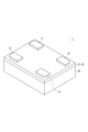
- FIG. 1 is a schematic perspective view showing the appearance of an electronic component 1 according to an embodiment of the technology disclosed herein.
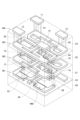
- FIG. 2 is a schematic exploded perspective view of the electronic component 1.
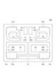
- FIG. 3 is a schematic plan view showing the pattern shape of the conductor layer M1.
- FIG. 4 is a schematic plan view showing the pattern shape of the conductor layer MM.
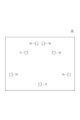
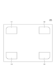
- FIG. 5 is a schematic plan view showing the positions of vias provided in the resin layer 21.
- FIG. FIG. 6 is a schematic plan view showing the pattern shape of the conductor layer M2.
- FIG. 7 is a schematic plan view showing the positions of vias provided in the resin layer 22.
- FIG. 8 is a schematic plan view showing the pattern shape of the conductor layer M3.
- FIG. 9 is a schematic plan view showing the positions of vias provided in the resin layer 23.
- FIG. 10 is a schematic plan view showing the pattern shape of the conductor layer M4.
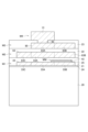
- FIG. 11 is a schematic partial cross-sectional view of the electronic component 1.
- FIG. 1 is a simplified perspective view showing the appearance of an electronic component 1 according to one embodiment of the technology disclosed herein.
- the electronic component 1 is a surface mount type LC filter, and includes a support substrate 20, a plurality of resin layers 21-23 laminated on the surface of the support substrate 20, and terminal electrodes 11-14 formed on the mounting surface.
- the material of the support substrate 20 is not particularly limited as long as it is chemically and thermally stable, generates little stress, and can maintain a smooth surface, and examples of the material that can be used include silicon single crystal, alumina, sapphire, aluminum nitride, MgO single crystal, SrTiO3 single crystal, surface silicon oxide, glass, quartz, and ferrite.
- FIG. 2 is a simplified exploded perspective view of electronic component 1.
- conductor layers M1, MM, M2, M3, and M4 made of Cu or the like are provided on the support substrate 20.
- conductor layer M1 is provided on a planarization layer 24 that covers the surface of the support substrate 20, and is embedded in a resin layer 21.
- Alumina, silicon oxide, or the like can be used as the planarization layer 24.
- Conductor layer M2 is provided on the upper surface of resin layer 21, and is embedded in resin layer 22.
- Conductor layer M3 is provided on the upper surface of resin layer 22, and is embedded in resin layer 23.
- Conductor layer M4 is made of terminal electrodes 11 to 14 provided on the upper surface of resin layer 23.
- Conductor layer MM is provided on the upper surface of conductor layer M1 via a capacitive insulating film (not shown), and is embedded in resin layer 21.
- the conductor layer M1 includes a number of conductor patterns 31-37. Of these, conductor patterns 31-34 overlap with terminal electrodes 11-14, respectively, in a planar view. Regions 11a-14a indicated by dashed lines in FIG. 3 are regions that overlap with terminal electrodes 11-14, respectively, in a planar view. The same is true in FIG. 6 and FIG. 8, which will be described later.
- the conductor pattern 33 is composed of a support portion 33A that at least partially overlaps the terminal electrode 13, and coil portions 33B and 33C that do not overlap the terminal electrode 13.
- the coil portions 33B and 33C are connected to different positions of the support portion 33A, so that the coil portions 33B and 33C are connected via the support portion 33A.
- the conductor pattern 34 is composed of a support portion 34A that at least partially overlaps the terminal electrode 14, and coil portions 34B and 34C that do not overlap the terminal electrode 14.
- the coil portions 34B and 34C are connected to different positions of the support portion 34A, so that the coil portions 34B and 34C are connected via the support portion 34A.
- the arrangement and shape of the portion where the support portion 33A and the coil portions 33B and 33C are connected are not particularly limited, and may be formed so that at least a portion of the coil portions overlap the terminal electrode 13 in a plan view, or may be formed at a position that does not overlap the terminal electrode 13. The same applies to the support portion 344A.
- the conductor layer MM includes a plurality of conductor patterns 43-46.
- the conductor patterns 43 and 45 are provided on the conductor pattern 33 located on the conductor layer M1 via a capacitive insulating film.
- the conductor patterns 44 and 46 are provided on the conductor pattern 34 located on the conductor layer M1 via a capacitive insulating film.
- the conductor patterns 43-46 function as upper electrodes of the capacitor, and parts of the conductor patterns 33 and 34 function as lower electrodes of the capacitor.
- the conductor pattern 43 overlaps with parts of the support portion 33A and the coil portion 33B of the conductor pattern 33.
- the conductor pattern 44 overlaps with parts of the support portion 34A and the coil portion 34B of the conductor pattern 34.
- the conductor patterns 43 and 44 at least partially overlap the terminal electrodes 13 and 14, respectively, in a plan view.
- the resin layer 21 is provided with a plurality of vias 51 to 58.
- the vias 51 and 52 expose the conductor pattern 33 located on the conductor layer M1
- the vias 57 and 58 expose the conductor pattern 34 located on the conductor layer M1
- the vias 53 to 56 expose the conductor patterns 43 to 46 located on the conductor layer MM.
- the vias 51 and 52 expose the coil parts 33B and 33C of the conductor pattern 33, respectively
- the vias 57 and 58 expose the coil parts 34B and 34C of the conductor pattern 34, respectively.
- the via 53 is disposed at a position overlapping the coil part 33B of the conductor pattern 33, and the via 54 is disposed at a position overlapping the coil part 34B of the conductor pattern 34.
- the resin layer 21 does not have vias at positions overlapping the support parts 31A to 34A, and the support parts 31A to 34A are entirely covered with the resin layer 21.
- the conductor layer M2 includes a plurality of conductor patterns 61-67.
- the conductor patterns 61-64 overlap the terminal electrodes 11-14, respectively, in a plan view.
- the conductor pattern 61 is made up of a support portion 61A that at least partially overlaps the terminal electrode 11, and coil portions 61B, 61C that do not overlap the terminal electrode 11.
- the conductor pattern 62 is made up of a support portion 62A that at least partially overlaps the terminal electrode 12, and coil portions 62B, 62C that do not overlap the terminal electrode 12.
- the conductor pattern 63 is made up of a support portion 63A that at least partially overlaps the terminal electrode 13, and coil portions 63B, 63C that do not overlap the terminal electrode 13.
- the conductor pattern 64 is made up of a support portion 64A that at least partially overlaps the terminal electrode 14, and coil portions 64B, 64C that do not overlap the terminal electrode 14.
- Coil portions 61B and 61C are connected to different positions of support portion 61A, and thus coil portions 61B and 61C are connected via support portion 61A.
- Coil portions 62B and 62C are connected to different positions of support portion 62A, and thus coil portions 62B and 62C are connected via support portion 62A.
- Coil portions 63B and 63C are connected to different positions of support portion 63A, and thus coil portions 63B and 63C are connected via support portion 63A.
- Coil portions 64B and 64C are connected to different positions of support portion 64A, and thus coil portions 64B and 64C are connected via support portion 64A.
- the arrangement and shape of the portion where support portion 61A and coil portions 61B and 61C are connected are not particularly limited, and may be formed so that at least a portion overlaps terminal electrode 11 in a plan view, or may be formed at a position that does not overlap terminal electrode 11.
- the coil portion 61B is connected to the coil portion 33B of the conductor pattern 33 located on the conductor layer M1 through a via 51 provided in the resin layer 21.
- the coil portion 62B is connected to the coil portion 34B of the conductor pattern 34 located on the conductor layer M1 through a via 57 provided in the resin layer 21.
- the coil portion 63B is connected to the coil portion 33C of the conductor pattern 33 located on the conductor layer M1 through a via 52 provided in the resin layer 21.
- the coil portion 64B is connected to the coil portion 34C of the conductor pattern 34 located on the conductor layer M1 through a via 58 provided in the resin layer 21.
- the conductor patterns 65 and 66 are connected to the conductor patterns 45 and 46 located on the conductor layer MM through vias 55 and 56 provided in the resin layer 21, respectively.
- the conductor pattern 67 is connected to the conductor patterns 43 and 44 located on the conductor layer MM through vias 53 and 54 provided in the resin layer 21.
- the resin layer 22 is provided with a plurality of vias 71-77. These vias 71-77 expose the conductor patterns 61-67 located on the conductor layer M2, respectively.
- via 71 is arranged at a position overlapping with the coil portion 61C of the conductor pattern 61
- via 72 is arranged at a position overlapping with the coil portion 62C of the conductor pattern 62
- via 73 is arranged at a position overlapping with the coil portion 63C of the conductor pattern 63
- via 74 is arranged at a position overlapping with the coil portion 64C of the conductor pattern 64.
- No vias are provided in the resin layer 22 at positions overlapping with the support portions 61A-64A, and the support portions 61A-64A are entirely covered with the resin layer 22.
- the conductor layer M3 includes a plurality of conductor patterns 80-82.
- conductor patterns 81 and 82 overlap terminal electrodes 11 and 12, respectively, in a planar view
- conductor pattern 83 overlaps terminal electrodes 13 and 14 in a planar view.
- Conductor pattern 81 consists of a support portion 81A that at least partially overlaps terminal electrode 11, and coil portions 81B and 81C that do not overlap terminal electrode 11.
- Conductor pattern 82 consists of a support portion 82A that at least partially overlaps terminal electrode 12, and coil portions 82B and 82C that do not overlap terminal electrode 12.
- Conductor pattern 80 consists of a support portion 83A that at least partially overlaps terminal electrode 13, a support portion 84A that at least partially overlaps terminal electrode 14, and coil portions 83B, 83C, and 80C that do not overlap terminal electrodes 13 and 14.
- the coil parts 81B and 81C are connected to different positions of the support part 81A, and thus the coil parts 81B and 81C are connected via the support part 81A.
- the coil parts 82B and 82C are connected to different positions of the support part 82A, and thus the coil parts 82B and 82C are connected via the support part 82A.
- the coil parts 83B and 80C are connected to different positions of the support part 83A, and thus the coil parts 83B and 80C are connected via the support part 83A.
- the coil parts 84B and 80C are connected to different positions of the support part 84A, and thus the coil parts 84B and 80C are connected via the support part 84A.
- the arrangement and shape of the part where the support part 81A and the coil parts 81B and 81C are connected are not particularly limited, and may be formed so that at least a part of it overlaps the terminal electrode 11 in a plan view, or may be formed in a position that does not overlap the terminal electrode 11.
- the coil portion 81B is connected to the coil portion 61C of the conductor pattern 61 located on the conductor layer M2 through a via 71 provided in the resin layer 22.
- the coil portion 81C is connected to the conductor pattern 65 located on the conductor layer M2 through a via 75 provided in the resin layer 22.
- the coil portion 82B is connected to the coil portion 62C of the conductor pattern 62 located on the conductor layer M2 through a via 72 provided in the resin layer 22.
- the coil portion 82C is connected to the conductor pattern 66 located on the conductor layer M2 through a via 76 provided in the resin layer 22.
- the coil portion 83B is connected to the coil portion 63C of the conductor pattern 63 located on the conductor layer M2 through a via 73 provided in the resin layer 22.
- the coil portion 84B is connected to the coil portion 64C of the conductor pattern 64 located on the conductor layer M2 through a via 74 provided in the resin layer 22.
- the coil portion 80C is connected to the conductor pattern 67 located on the conductor layer M2 through a via 77 provided in the resin layer 22.
- the resin layer 23 has a plurality of vias 91-94. These vias 91-94 expose the support portions 81A-84A located on the conductor layer M3, respectively. Therefore, the vias 91-94 overlap with the terminal electrodes 11-14, respectively.
- the conductor layer M4 includes a plurality of terminal electrodes 11-14. These terminal electrodes 11-14 are connected to the support portions 81A-84A located on the conductor layer M3 through vias 91-94, respectively.
- an inductor consisting of the coil portion 81B and the conductor pattern 61, and a capacitor with the conductor pattern 45 as the upper electrode are connected in parallel between the terminal electrode 11 and the conductor pattern 33.
- an inductor consisting of the coil portion 82B and the conductor pattern 62, and a capacitor with the conductor pattern 46 as the upper electrode are connected in parallel between the terminal electrode 12 and the conductor pattern 34.
- an inductor consisting of the coil portion 83B and the conductor pattern 63, and a capacitor with the conductor pattern 43 as the upper electrode are connected in parallel between the terminal electrode 13 and the conductor pattern 33.
- an inductor consisting of the coil portion 84B and the conductor pattern 64, and a capacitor with the conductor pattern 44 as the upper electrode are connected in parallel between the terminal electrode 14 and the conductor pattern 34.
- the conductor patterns 33 and 34 themselves also function as inductors. This constitutes an LC filter with the terminal electrodes 11 and 12 as input/output terminals and the terminal electrodes 13 and 14 as ground terminals.
- FIG. 11 is a schematic partial cross-sectional view of electronic component 1.
- the terminal electrode 13 directly below the terminal electrode 13 are provided a conductor pattern 80 located on conductor layer M3, a conductor pattern 63 located on conductor layer M2, and a conductor pattern 33 located on conductor layer M1.
- the terminal electrode 13 is connected to the support portion 83A of the conductor pattern 80 via a via 93 provided in the resin layer 23. In this way, the terminal electrode 13 is connected to the support portion 83A of the conductor pattern 80 located directly below via the via 93, thereby increasing the fixing strength.
- the resin layer 22 does not have a via connecting the support portion 83A of the conductor pattern 80 to the support portion 63A of the conductor pattern 63, and similarly, the resin layer 21 does not have a via connecting the support portion 63A of the conductor pattern 63 to the support portion 33A of the conductor pattern 33.
- the stress applied to the electronic component 1 through the terminal electrode 13 is absorbed by the resin layers 21 and 22, so that the lower conductor layer is less likely to be damaged.
- the capacitor is less likely to be damaged, so that capacitance fluctuations caused by damage can be suppressed.
- the area in which the upper electrode of the capacitor can be arranged is expanded, which increases the design freedom.
- coil portions 63B and 63C located on conductor layer M2 are connected to each other via support portion 63A, so that support portion 63A functions as part of the coil pattern.
- coil portions 33B and 33C located on conductor layer M1 are connected to each other via support portion 33A, so that support portion 33A functions as part of the coil pattern.
- a portion of the coil pattern is positioned so as to overlap terminal electrode 13, so that it is possible to obtain sufficient inductance while keeping the chip size small.
- the conductor pattern located on the conductor layer M3 is connected to the terminal electrodes 11-14 directly above it through vias, while the areas of the conductor patterns located on the conductor layers M1 and M2 that overlap with the terminal electrodes 11-14 are covered on the front with a resin layer, which alleviates the stress applied to the electronic component 1 through the terminal electrodes 11-14 and makes it possible to obtain a larger inductance while keeping the chip size small.
- support portions 33A, 63A, 83A may completely overlap terminal electrode 13 when viewed in a plane from the terminal electrode side, or may not overlap at least partially.
- support portions 34A, 64A, 84A may completely overlap terminal electrode 14 when viewed in a plane from the terminal electrode side, or may not overlap at least partially.
- Support portions 61A, 81A may completely overlap terminal electrode 11 when viewed in a plane from the terminal electrode side, or may not overlap at least partially.
- Support portions 62A, 82A may completely overlap terminal electrode 12 when viewed in a plane from the terminal electrode side, or may not overlap at least partially.
- An electronic component comprises a first conductor layer, a first resin layer in which the first conductor layer is embedded, a second conductor layer formed on an upper surface of the first resin layer or on an upper surface of another resin layer covering the first resin layer, a second resin layer covering the upper surface of the first resin layer so as to embed the second conductor layer, and a terminal electrode formed on the upper surface of the second resin layer, wherein the first conductor layer includes a first conductor pattern, and the second conductor layer includes a second conductor pattern, wherein the first conductor pattern includes a first support portion at least partially overlapping with the terminal electrode, and first and second coil portions connected to the first support portion without overlapping with the terminal electrodes, wherein the second conductor pattern includes a second support portion overlapping with the terminal electrode and connected to the terminal electrode through a via provided in the second resin layer, and a third coil portion connected to the second support portion without overlapping with the terminal electrode, wherein the first coil portion and the second coil portion are electrically connected via the first support portion,
- the electronic component further includes a third conductor layer and a third resin layer in which the third conductor layer is embedded, the first conductor layer is formed on the upper surface of the third resin layer, the third conductor layer includes a third conductor pattern, the third conductor pattern includes a third support portion that at least partially overlaps with the terminal electrode, and fourth and fifth coil portions connected to the third support portion without overlapping with the terminal electrode, the fourth coil portion and the fifth coil portion being electrically connected via the third support portion, and the third support portion may be entirely covered with the third resin layer. This reduces stress applied to the first and third conductor layers via the terminal electrodes and increases the utilization efficiency of the first and third conductor layers.
- the electronic component further includes a third conductor layer formed on the upper surface of the first resin layer, and a third resin layer covering the upper surface of the first resin layer so as to embed the third conductor layer, the second conductor layer being formed on the upper surface of the third resin layer, the third conductor layer including a third conductor pattern, the third conductor pattern including a third support portion at least partially overlapping with the terminal electrode, and fourth and fifth coil portions connected to the third support portion without overlapping with the terminal electrode, the fourth coil portion and the fifth coil portion being electrically connected via the third support portion, and the third support portion may be entirely covered with the third resin layer. This reduces stress applied to the first and third conductor layers via the terminal electrodes, and improves the utilization efficiency of the first and third conductor layers.
- the electronic component further includes a third conductor layer and a third resin layer in which the third conductor layer is embedded, the first conductor layer being formed on the upper surface of the third resin layer, the third conductor layer including a third conductor pattern, the third conductor pattern including a third support portion at least partially overlapping with the terminal electrode, and a lower electrode partially overlapping with the terminal electrode and the remaining portion not overlapping with the terminal electrode, and the lower electrode may be covered with the upper electrode via a capacitive insulating film. This expands the area in which the upper electrode of the capacitor can be arranged, thereby increasing design freedom.
Landscapes
- Engineering & Computer Science (AREA)
- Power Engineering (AREA)
- Microelectronics & Electronic Packaging (AREA)
- Manufacturing & Machinery (AREA)
- Coils Or Transformers For Communication (AREA)
Abstract
Description
11~14 端子電極
11a~14a 端子電極と重なる領域
20 支持基板
21~23 樹脂層
24 平坦化層
25 容量絶縁膜
31~37 導体パターン
33A,34A サポート部
33B,33C,34B,34C コイル部
43~46 導体パターン
51~58 ビア
61~67 導体パターン
61A~64A サポート部
61B~64B,61C~64C コイル部
71~77 ビア
80~82 導体パターン
81A~84A サポート部
81B~84B,80C~82C コイル部
91~94 ビア
M1,MM,M2,M3,M4 導体層
Claims (4)
- 第1導体層と、
前記第1導体層を埋め込む第1樹脂層と、
前記第1樹脂層の上面、或いは、前記第1樹脂層を覆う他の樹脂層の上面に形成された第2導体層と、
前記第2導体層を埋め込むよう、前記第1樹脂層の前記上面を覆う第2樹脂層と、
第2樹脂層の上面に形成された端子電極と、を備え、
前記第1導体層は、第1導体パターンを含み、
前記第2導体層は、第2導体パターンを含み、
前記第1導体パターンは、前記端子電極と少なくとも一部が重なる第1サポート部と、前記端子電極と重なることなく前記第1サポート部に接続された第1及び第2コイル部とを含み、
前記第2導体パターンは、前記端子電極と重なるとともに前記第2樹脂層に設けられたビアを介して前記端子電極に接続された第2サポート部と、前記端子電極と重なることなく前記第2サポート部に接続された第3コイル部とを含み、
前記第1コイル部と前記第2コイル部は、前記第1サポート部を介して電気的に接続され、
前記第1サポート部は、全面が前記第1樹脂層で覆われている、電子部品。 - 第3導体層と、
前記第3導体層を埋め込む第3樹脂層と、をさらに備え、
前記第1導体層は、前記第3樹脂層の上面に形成され、
前記第3導体層は、第3導体パターンを含み、
前記第3導体パターンは、前記端子電極と少なくとも一部が重なる第3サポート部と、前記端子電極と重なることなく前記第3サポート部に接続された第4及び第5コイル部とを含み、
前記第4コイル部と前記第5コイル部は、前記第3サポート部を介して電気的に接続され、
前記第3サポート部は、全面が前記第3樹脂層で覆われている、請求項1に記載の電子部品。 - 前記第1樹脂層の上面に形成された第3導体層と、
前記第3導体層を埋め込むよう、前記第1樹脂層の前記上面を覆う第3樹脂層と、をさらに備え、
前記第2導体層は、前記第3樹脂層の上面に形成され、
前記第3導体層は、第3導体パターンを含み、
前記第3導体パターンは、前記端子電極と少なくとも一部が重なる第3サポート部と、前記端子電極と重なることなく前記第3サポート部に接続された第4及び第5コイル部とを含み、
前記第4コイル部と前記第5コイル部は、前記第3サポート部を介して電気的に接続され、
前記第3サポート部は、全面が前記第3樹脂層で覆われている、請求項1に記載の電子部品。 - 第3導体層と、
前記第3導体層を埋め込む第3樹脂層と、をさらに備え、
前記第1導体層は、前記第3樹脂層の上面に形成され、
前記第3導体層は、第3導体パターンを含み、
前記第3導体パターンは、前記端子電極と少なくとも一部が重なる第3サポート部と、一部が前記端子電極と重なり、残りの部分が前記端子電極と重ならない下部電極とを含み、
前記下部電極は、容量絶縁膜を介して上部電極で覆われる、請求項1に記載の電子部品。
Priority Applications (2)
| Application Number | Priority Date | Filing Date | Title |
|---|---|---|---|
| JP2024557061A JPWO2024101032A1 (ja) | 2022-11-10 | 2023-10-02 | |
| CN202380077187.2A CN120153447A (zh) | 2022-11-10 | 2023-10-02 | 电子部件 |
Applications Claiming Priority (2)
| Application Number | Priority Date | Filing Date | Title |
|---|---|---|---|
| JP2022180499 | 2022-11-10 | ||
| JP2022-180499 | 2022-11-10 |
Publications (1)
| Publication Number | Publication Date |
|---|---|
| WO2024101032A1 true WO2024101032A1 (ja) | 2024-05-16 |
Family
ID=91032574
Family Applications (1)
| Application Number | Title | Priority Date | Filing Date |
|---|---|---|---|
| PCT/JP2023/035888 Ceased WO2024101032A1 (ja) | 2022-11-10 | 2023-10-02 | 電子部品 |
Country Status (3)
| Country | Link |
|---|---|
| JP (1) | JPWO2024101032A1 (ja) |
| CN (1) | CN120153447A (ja) |
| WO (1) | WO2024101032A1 (ja) |
Citations (4)
| Publication number | Priority date | Publication date | Assignee | Title |
|---|---|---|---|---|
| JP2000173835A (ja) * | 1998-12-05 | 2000-06-23 | Tdk Corp | 積層電子部品及びその製造方法 |
| WO2015005161A1 (ja) * | 2013-07-11 | 2015-01-15 | 株式会社村田製作所 | 電子部品 |
| JP2021106223A (ja) * | 2019-12-26 | 2021-07-26 | Tdk株式会社 | 電子部品 |
| JP2022055128A (ja) * | 2020-09-28 | 2022-04-07 | Tdk株式会社 | 電子部品 |
-
2023
- 2023-10-02 WO PCT/JP2023/035888 patent/WO2024101032A1/ja not_active Ceased
- 2023-10-02 CN CN202380077187.2A patent/CN120153447A/zh active Pending
- 2023-10-02 JP JP2024557061A patent/JPWO2024101032A1/ja active Pending
Patent Citations (4)
| Publication number | Priority date | Publication date | Assignee | Title |
|---|---|---|---|---|
| JP2000173835A (ja) * | 1998-12-05 | 2000-06-23 | Tdk Corp | 積層電子部品及びその製造方法 |
| WO2015005161A1 (ja) * | 2013-07-11 | 2015-01-15 | 株式会社村田製作所 | 電子部品 |
| JP2021106223A (ja) * | 2019-12-26 | 2021-07-26 | Tdk株式会社 | 電子部品 |
| JP2022055128A (ja) * | 2020-09-28 | 2022-04-07 | Tdk株式会社 | 電子部品 |
Also Published As
| Publication number | Publication date |
|---|---|
| CN120153447A (zh) | 2025-06-13 |
| JPWO2024101032A1 (ja) | 2024-05-16 |
Similar Documents
| Publication | Publication Date | Title |
|---|---|---|
| US8050045B2 (en) | Electronic component and method of manufacturing the same | |
| US7339452B2 (en) | Embedded inductor and application thereof | |
| JP7473437B2 (ja) | 電子部品 | |
| US7633368B2 (en) | On-chip inductor | |
| WO2009082003A1 (ja) | 電磁バンドギャップ素子及びそれを用いたアンテナ並びにフィルタ | |
| US8705247B2 (en) | Circuit board and mother laminated body | |
| US6476695B1 (en) | High frequency module | |
| JP7602397B2 (ja) | 電子部品及びその製造方法 | |
| JP5138260B2 (ja) | チップ型電子部品 | |
| JP2009164560A (ja) | 実装構造体、電気光学装置及び電子機器 | |
| US7449772B2 (en) | Chip-type electronic component including thin-film circuit elements | |
| US20240194396A1 (en) | Inductor component | |
| US11798469B1 (en) | Display panel and display device | |
| CN120153447A (zh) | 电子部件 | |
| US20070086145A1 (en) | Capacitor-built-in substrate and method of manufacturing the same | |
| CN113314564B (zh) | 电子装置 | |
| US20230093838A1 (en) | Electronic component | |
| US20250149218A1 (en) | Inductor component | |
| US20250168978A1 (en) | Electronic component | |
| JP3936620B2 (ja) | 高周波モジュール | |
| JP7734022B2 (ja) | Lc複合電子部品 | |
| JP4417235B2 (ja) | 発振器 | |
| WO2024111251A1 (ja) | 電子部品 | |
| JP6256575B2 (ja) | 高周波モジュール | |
| JP3936619B2 (ja) | 高周波モジュール |
Legal Events
| Date | Code | Title | Description |
|---|---|---|---|
| 121 | Ep: the epo has been informed by wipo that ep was designated in this application |
Ref document number: 23888385 Country of ref document: EP Kind code of ref document: A1 |
|
| WWE | Wipo information: entry into national phase |
Ref document number: 2024557061 Country of ref document: JP |
|
| WWE | Wipo information: entry into national phase |
Ref document number: 202380077187.2 Country of ref document: CN |
|
| NENP | Non-entry into the national phase |
Ref country code: DE |
|
| WWP | Wipo information: published in national office |
Ref document number: 202380077187.2 Country of ref document: CN |
|
| 122 | Ep: pct application non-entry in european phase |
Ref document number: 23888385 Country of ref document: EP Kind code of ref document: A1 |