WO2024100973A1 - 積層セラミックコンデンサ - Google Patents
積層セラミックコンデンサ Download PDFInfo
- Publication number
- WO2024100973A1 WO2024100973A1 PCT/JP2023/032095 JP2023032095W WO2024100973A1 WO 2024100973 A1 WO2024100973 A1 WO 2024100973A1 JP 2023032095 W JP2023032095 W JP 2023032095W WO 2024100973 A1 WO2024100973 A1 WO 2024100973A1
- Authority
- WO
- WIPO (PCT)
- Prior art keywords
- horizontal portion
- shoulder
- laminate
- external electrode
- layer
- Prior art date
- Legal status (The legal status is an assumption and is not a legal conclusion. Google has not performed a legal analysis and makes no representation as to the accuracy of the status listed.)
- Ceased
Links
Images


Classifications
-
- H—ELECTRICITY
- H01—ELECTRIC ELEMENTS
- H01G—CAPACITORS; CAPACITORS, RECTIFIERS, DETECTORS, SWITCHING DEVICES, LIGHT-SENSITIVE OR TEMPERATURE-SENSITIVE DEVICES OF THE ELECTROLYTIC TYPE
- H01G4/00—Fixed capacitors; Processes of their manufacture
- H01G4/30—Stacked capacitors
-
- H—ELECTRICITY
- H01—ELECTRIC ELEMENTS
- H01G—CAPACITORS; CAPACITORS, RECTIFIERS, DETECTORS, SWITCHING DEVICES, LIGHT-SENSITIVE OR TEMPERATURE-SENSITIVE DEVICES OF THE ELECTROLYTIC TYPE
- H01G2/00—Details of capacitors not covered by a single one of groups H01G4/00-H01G11/00
- H01G2/02—Mountings
- H01G2/06—Mountings specially adapted for mounting on a printed-circuit support
- H01G2/065—Mountings specially adapted for mounting on a printed-circuit support for surface mounting, e.g. chip capacitors
-
- H—ELECTRICITY
- H01—ELECTRIC ELEMENTS
- H01G—CAPACITORS; CAPACITORS, RECTIFIERS, DETECTORS, SWITCHING DEVICES, LIGHT-SENSITIVE OR TEMPERATURE-SENSITIVE DEVICES OF THE ELECTROLYTIC TYPE
- H01G4/00—Fixed capacitors; Processes of their manufacture
- H01G4/002—Details
- H01G4/005—Electrodes
- H01G4/008—Selection of materials
-
- H—ELECTRICITY
- H01—ELECTRIC ELEMENTS
- H01G—CAPACITORS; CAPACITORS, RECTIFIERS, DETECTORS, SWITCHING DEVICES, LIGHT-SENSITIVE OR TEMPERATURE-SENSITIVE DEVICES OF THE ELECTROLYTIC TYPE
- H01G4/00—Fixed capacitors; Processes of their manufacture
- H01G4/002—Details
- H01G4/005—Electrodes
- H01G4/012—Form of non-self-supporting electrodes
-
- H—ELECTRICITY
- H01—ELECTRIC ELEMENTS
- H01G—CAPACITORS; CAPACITORS, RECTIFIERS, DETECTORS, SWITCHING DEVICES, LIGHT-SENSITIVE OR TEMPERATURE-SENSITIVE DEVICES OF THE ELECTROLYTIC TYPE
- H01G4/00—Fixed capacitors; Processes of their manufacture
- H01G4/002—Details
- H01G4/018—Dielectrics
- H01G4/06—Solid dielectrics
- H01G4/08—Inorganic dielectrics
- H01G4/12—Ceramic dielectrics
- H01G4/1209—Ceramic dielectrics characterised by the ceramic dielectric material
- H01G4/1218—Ceramic dielectrics characterised by the ceramic dielectric material based on titanium oxides or titanates
- H01G4/1227—Ceramic dielectrics characterised by the ceramic dielectric material based on titanium oxides or titanates based on alkaline earth titanates
-
- H—ELECTRICITY
- H01—ELECTRIC ELEMENTS
- H01G—CAPACITORS; CAPACITORS, RECTIFIERS, DETECTORS, SWITCHING DEVICES, LIGHT-SENSITIVE OR TEMPERATURE-SENSITIVE DEVICES OF THE ELECTROLYTIC TYPE
- H01G4/00—Fixed capacitors; Processes of their manufacture
- H01G4/002—Details
- H01G4/224—Housing; Encapsulation
-
- H—ELECTRICITY
- H01—ELECTRIC ELEMENTS
- H01G—CAPACITORS; CAPACITORS, RECTIFIERS, DETECTORS, SWITCHING DEVICES, LIGHT-SENSITIVE OR TEMPERATURE-SENSITIVE DEVICES OF THE ELECTROLYTIC TYPE
- H01G4/00—Fixed capacitors; Processes of their manufacture
- H01G4/002—Details
- H01G4/228—Terminals
- H01G4/232—Terminals electrically connecting two or more layers of a stacked or rolled capacitor
- H01G4/2325—Terminals electrically connecting two or more layers of a stacked or rolled capacitor characterised by the material of the terminals
Definitions
- the present invention relates to a multilayer ceramic capacitor.
- a display module that includes a flexible housing, multiple non-flexible substrates built into the housing, and a flexible substrate that connects the multiple substrates.
- This display module is flexible as a whole, so it can be used even in a bent state.
- a non-flexible substrate is connected to the display module, and electronic components are mounted on the substrate. Among these electronic components is a multilayer ceramic capacitor.
- An object of the present invention is to provide a multilayer ceramic capacitor that can improve stability when mounted on a substrate and that prevents the multilayer ceramic capacitor from coming into contact with a housing.
- Multilayer ceramic capacitors are A plurality of dielectric layers and a plurality of internal electrode layers are stacked, a laminate having a first main surface and a second main surface opposed to each other in a stacking direction, a first side surface and a second side surface opposed to each other in a width direction perpendicular to the stacking direction, and a first end surface and a second end surface opposed to each other in a length direction perpendicular to the stacking direction and the width direction; an external electrode disposed on the first end surface and the second end surface and connected to the internal electrode layer; the external electrodes each extend to at least a portion of the first main surface, the second main surface, the first side surface, and the second side surface;
- a cross section parallel to the width direction and the stacking direction is a WT cross section, a cross section parallel to the length direction and the stacking direction is a LT cross section, and a cross section parallel to the width direction and the length direction is a WL cross section, When viewed in the WT cross section, the external electrode
- the present invention provides a multilayer ceramic capacitor that can improve stability when mounted on a substrate and prevents the housing from coming into contact with the multilayer ceramic capacitor.
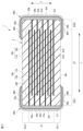
- FIG. 1 is a perspective view of a multilayer ceramic capacitor according to the present invention
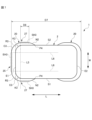
- 2 is a cross-sectional view taken along line II in FIG. 1.
- 2 is a cross-sectional view taken along line II-II of FIG. 1.
- FIG. 2 is a diagram illustrating a WT cross section of an external electrode.
- FIG. 13 is a diagram for explaining a horizontal portion.
- FIG. 2 is a diagram illustrating an LT cross section of a multilayer ceramic capacitor.
- FIG. 2 is a diagram illustrating a schematic LW cross section of a multilayer ceramic capacitor.
- Fig. 1 is a perspective view showing the multilayer ceramic capacitor 1 of the present embodiment.
- the multilayer ceramic capacitor 1 includes a laminate 2 and external electrodes 20.
- the external electrodes 20 include a first external electrode 20a and a second external electrode 20b.
- ⁇ Direction definition> 1 to 7 show an L direction, a W direction, and a T direction.
- the L direction is the length direction L of the multilayer ceramic capacitor 1.
- the W direction is the width direction W of the multilayer ceramic capacitor 1.
- the T direction is the lamination direction T of the multilayer ceramic capacitor 1. 2 is referred to as the LT cross section, and the cross section shown in FIG. 3 is referred to as the WT cross section.
- the length direction L, the width direction W, and the stacking direction T do not necessarily have to be perpendicular to each other.
- the length direction L, the width direction W, and the stacking direction T may intersect each other.
- the laminate 2 has a substantially rectangular parallelepiped shape.
- the laminate has two main surfaces M, two end surfaces E, and two side surfaces S.
- the main surfaces M are surfaces facing the stacking direction T.
- the end surfaces E are surfaces facing the length direction L.
- the side surfaces S are surfaces facing the width direction W.
- the two main surfaces M are a first main surface M1 and a second main surface M2.
- the two end surfaces E are a first end surface E1 and a second end surface E2.
- the two side surfaces S are a first side surface S1 and a second side surface S2.
- the ridges and corners of the laminate 2 are preferably rounded.
- a ridge is a portion where two surfaces of the laminate 2 intersect.
- a corner is a portion where three surfaces of the laminate 2 intersect.
- the size of the laminate 2 is not particularly limited.
- the length in the longitudinal direction L of the laminate 2 may be 0.05 mm or more and 1.00 mm or less.
- the length in the stacking direction T of the laminate 2 may be 0.10 mm or more and 0.50 mm or less.
- the length in the width direction W of the laminate 2 may be 0.10 mm or more and 0.50 mm or less.
- the length of each portion of the laminate 2 can be measured with a micrometer or an optical microscope.
- the length in the length direction L does not necessarily have to be longer than the length in the width direction W.
- the external electrodes 20 are provided with horizontal portions H having a predetermined shape. Specifically, a main surface horizontal portion MH, a side surface horizontal portion SH, and an end surface horizontal portion EH are provided on the external electrode 20. These horizontal portions H will be described later.
- Fig. 2 is a cross-sectional view of the laminate ceramic capacitor shown in Fig. 1 taken along line II.
- the laminate 2 includes a plurality of dielectric layers 4 and a plurality of internal electrode layers 10.
- the plurality of dielectric layers 4 and the plurality of internal electrode layers 10 are stacked in a stacking direction T on top of each other.
- the laminate 2 has an inner layer portion IL and an outer layer portion OL in the stacking direction T.
- the outer layer portion OL includes a first outer layer portion OL1 and a second outer layer portion OL2.
- the first outer layer portion OL1 and the second outer layer portion OL2 are arranged to sandwich the inner layer portion IL in the stacking direction T.
- the inner layer portion IL includes some of the dielectric layers 4 and a plurality of internal electrode layers 10.
- the plurality of internal electrode layers 10 are disposed to face each other with the dielectric layer 4 interposed therebetween.
- the inner layer portion IL is a portion where a capacitance is formed and essentially functions as a capacitor, and is therefore also called an effective portion.
- the first outer layer portion OL1 is disposed on the first main surface M1 side of the laminate 2.
- the second outer layer portion OL2 is disposed on the second main surface M2 side of the laminate 2.
- the first outer layer portion OL1 is disposed between the first main surface M1 and an internal electrode layer 10 that is closest to the first main surface M1 among the multiple internal electrode layers 10.
- the second outer layer portion OL2 is disposed between the second main surface M2 and an internal electrode layer 10 that is closest to the second main surface M2 among the multiple internal electrode layers 10.
- the first outer layer portion OL1 and the second outer layer portion OL2 do not include the internal electrode layer 10.
- the first outer layer portion OL1 and the second outer layer portion OL2 include the remaining dielectric layers 4, among the plurality of dielectric layers 4, excluding the dielectric layers 4 for the inner layer portion IL.
- the first outer layer portion OL1 and the second outer layer portion OL2 function as protective layers for the inner layer portion IL.
- the dielectric layer 4 includes an outer dielectric layer 5 and an inner dielectric layer 6 .
- the outer dielectric layer 5 is a dielectric layer 4 constituting the first outer layer portion OL1 and the second outer layer portion OL2 of the dielectric layer 4.
- the outer dielectric layer 5 is disposed between the first main surface M1 and the internal electrode layer 10 closest to the first main surface M1, and between the second main surface M2 and the internal electrode layer 10 closest to the second main surface M2.
- the inner dielectric layer 6 is a dielectric layer 4 located between the internal electrode layers 10 and constituting the inner layer portion IL together with the internal electrode layers 10 .
- the inner dielectric layer 6 is disposed between a first inner electrode layer 10a and a second inner electrode layer 10b which will be described below.
- the number of dielectric layers 4 laminated in the laminate 2 can be, for example, from 10 to 2000.
- the number of dielectric layers 4 includes the number of outer dielectric layers 5 and the number of inner dielectric layers 6.
- the outer dielectric layer 5 may have a thickness of, for example, 10 ⁇ m or more and 100 ⁇ m or less
- the inner dielectric layer 6 may have a thickness of, for example, 0.8 ⁇ m or more and 3.0 ⁇ m or less.
- the material of the dielectric layer 4 may be a dielectric ceramic, for example, including BaTiO3 , CaTiO3 , SrTiO3 , CaZrO3 , or TiO2 .
- the material of the dielectric layer 4 may be the above-mentioned dielectric ceramic to which a Mn compound, an Fe compound, a Cr compound, a Co compound, an Ni compound, or the like has been added in an amount less than that of the main component.
- the internal electrode layer 10 includes a first internal electrode layer 10a and a second internal electrode layer 10b.
- the first internal electrode layer 10a is the internal electrode layer 10 connected to the first external electrode 20a.
- the second internal electrode layer 10b is the internal electrode layer 10 connected to the second external electrode 20b.
- the first internal electrode layer 10a extends from the first end face E1 toward the second end face E2, and the second internal electrode layer 10b extends from the second end face E2 toward the first end face E1.
- the first internal electrode layer 10 a and the second internal electrode layer 10 b each have a counter electrode portion 11 and an extraction electrode portion 12 .
- the opposing electrode portion 11 is a portion of the internal electrode layer 10 where the first internal electrode layer 10a and the second internal electrode layer 10b face each other in the stacking direction T.
- the extraction electrode portion 12 is a portion of the internal electrode layer 10 that is extracted from the opposing electrode portion 11 to the end face E1 or the end face E2 of the laminate 2.
- the opposing electrode portion 11 of the first internal electrode layer 10a is referred to as a first opposing electrode portion 11a
- the lead electrode portion 12 of the first internal electrode layer 10a is referred to as a first lead electrode portion 12a.
- the first lead electrode portion 12a is a portion that is led out from the first opposing electrode portion 11a to the first end face E1 of the laminate 2.
- the opposing electrode portion 11 of the second internal electrode layer 10b is referred to as a second opposing electrode portion 11b
- the lead electrode portion 12 of the second internal electrode layer 10b is referred to as a second lead electrode portion 12b.
- the second lead electrode portion 12b is a portion that is led out from the second opposing electrode portion 11b to the second end face E2 of the laminate 2.
- the number of the internal electrode layers 10 can be, for example, from 10 to 1000.
- the number of the internal electrode layers 10 includes the number of the first internal electrode layers 10a and the number of the second internal electrode layers 10b.
- the thickness of the internal electrode layer 10 can be, for example, not less than 0.3 ⁇ m and not more than 0.4 ⁇ m.
- the material of the internal electrode layer 10 can be, for example, metals such as Ni, Cu, Ag, Pd, and Au, alloys of Ni and Cu, alloys of Ag and Pd, etc.
- the material of the internal electrode layer 10 may contain dielectric particles of the same composition as the ceramic contained in the dielectric layer 4.
- the laminate 2 has an electrode opposing portion LF and an end gap portion EG in the longitudinal direction L.
- the end gap portion EG includes a first end gap portion EG1 and a second end gap portion EG2.
- the electrode opposing portion LF is a portion where the first internal electrode layer 10a and the second internal electrode layer 10b oppose each other in the stacking direction T.
- the electrode opposing portion LF is a portion where the first opposing electrode portion 11a and the second opposing electrode portion 11b oppose each other in the stacking direction T.
- the electrode facing portion LF is located at the center in the longitudinal direction L of the laminate 2 .
- the electrode facing portion LF is a portion where a capacitance is formed, and is a portion that essentially functions as a capacitor. For this reason, the electrode facing portion LF is also called an effective portion.
- the end gap portion EG is a portion where the first internal electrode layer 10a and the second internal electrode layer 10b do not face each other in the stacking direction T. Specifically, in the stacking direction T, a portion where the first internal electrode layer 10a is arranged and the second internal electrode layer 10b is not arranged is a first end gap portion EG1. Similarly, a portion where the second internal electrode layer 10b is arranged and the first internal electrode layer 10a is not arranged is a second end gap portion EG2.
- the first end gap portion EG1 corresponds to the portion where the first extension electrode portion 12a is disposed
- the second end gap portion EG2 corresponds to the portion where the second extension electrode portion 12b is disposed.
- the first end gap portion EG1 functions as an extraction electrode to the first end face E1 of the first internal electrode layer 10a
- the second end gap portion EG2 functions as an extraction electrode to the second end face E2 of the second internal electrode layer 10b.
- the end gap portion EG is a section in the length direction L, and is therefore also called an L gap.
- the length of the end gap portion EG in the longitudinal direction L can be, for example, 5 ⁇ m or more and 30 ⁇ m or less.
- the external electrodes include a first external electrode 20a and a second external electrode 20b.
- the first external electrode 20a is an external electrode disposed on the first end face E1 of the laminate 2.
- the first external electrode 20a is electrically connected to the first internal electrode layer 10a.
- the second external electrode 20b is an external electrode disposed on the second end face E2 of the laminate 2.
- the second external electrode 20b is electrically connected to the second internal electrode layer 10b.
- the external electrode 20 extends from the end face E to parts of the two main faces M and to parts of the two side faces S.
- a portion arranged on the end face E is referred to as an end face external electrode 25.
- a portion arranged on a part of the main face M is referred to as a main face external electrode 26.
- a portion arranged on a part of the side face S is referred to as a side face external electrode 27.
- the portion of the first external electrode 20a that is arranged on the first end face E1 is referred to as the first end face external electrode 25a.
- the portion of the first external electrode 20a that is arranged on a part of the first main face M1 or a part of the second main face M2 is referred to as the first main face external electrode 26a.
- the portion of the first external electrode 20a that is arranged on a part of the first side face S1 or a part of the second side face S2 is referred to as the first side face external electrode 27a.
- the portion of the second external electrode 20b that is arranged on the second end face E2 is referred to as the second end face external electrode 25b.
- the portion of the second external electrode 20b that is arranged on a part of the first main face M1 or a part of the second main face M2 is referred to as the second main face external electrode 26b.
- the portion of the second external electrode 20b that is arranged on a part of the first side face S1 or a part of the second side face S2 is referred to as the second side face external electrode 27b.
- the above-mentioned main surface horizontal portion MH is provided on the first main surface external electrode 26a and the second main surface external electrode 26b. Also, the end surface horizontal portion EH is provided on the first end surface external electrode 25a and the second end surface external electrode 25b.
- the layer structure of the external electrode 20 will be described with reference to FIG.
- the external electrode 20 includes three layers: a base electrode layer 21, an inner plating layer 23, and a surface plating layer 24. These layers are arranged in the following order from the end face E of the laminate 2: the base electrode layer 21, the inner plating layer 23, and the surface plating layer 24.
- the first external electrode 20a includes a first base electrode layer 21a, a first inner plating layer 23a, and a first surface plating layer 24a.
- the second external electrode 20b includes a second base electrode layer 21b, a second inner plating layer 23b, and a second surface plating layer 24b.
- the direction away from the end face E of the laminate 2 may be referred to as the "up" side.
- the resin electrode layer 22 may be described as being disposed on the base electrode layer 21.
- the first base electrode layer 21a is disposed on and covers the first end face E1 of the laminate 2.
- the first base electrode layer 21a may extend from the first end face E1 to a part of the first main surface M1, a part of the second main surface M2, a part of the first side surface S1, and a part of the second side surface S2.
- the second base electrode layer 21b is disposed on the second end face E2 of the laminate 2 and covers the second end face E2.
- the second base electrode layer 21b may extend from the second end face E2 to a portion of the second main surface M1, a portion of the second main surface M2, a portion of the first side surface S1, and a portion of the second side surface S2.
- the base electrode layer 21 may be a fired layer containing metal and glass.
- the fired layer is a layer formed by applying a conductive paste containing metal and glass to a laminate by a dipping method and firing the laminate.
- the firing for forming the fired layer may be performed after firing the internal electrode layer, or may be performed simultaneously with firing the internal electrode layer.
- the fired layer may be a multi-layer structure.
- the metal contained in the fired layer contains Cu as a main component.
- the metal may contain at least one selected from metals such as Ni, Ag, Pd, or Au, or an alloy such as an Ag-Pd alloy, as a main component, or may contain it as a component other than the main component.
- the glass contained in the fired layer may be a glass component containing at least one element selected from B, Si, Ba, Mg, Al, Li, etc.
- borosilicate glass may be used.
- the base electrode layer 21 may also be a resin layer containing conductive particles and a thermosetting resin.
- the resin layer may be formed on the above-mentioned fired layer, or may be formed directly on the laminate without forming a fired layer.
- the resin layer is a layer formed by applying a conductive paste containing conductive particles and a thermosetting resin to the laminate by a coating method and then firing the layer.
- the resin layer may be fired after firing the internal electrode layer, or may be fired simultaneously with the internal electrode layer.
- the resin layer may also be a multi-layer structure.
- each of the base electrode layers 21 as a fired layer or resin layer is not particularly limited and may be 1 ⁇ m or more and 10 ⁇ m or less.
- the base electrode layer 21 may also be a thin film layer of 1 ⁇ m or less formed by a thin film formation method such as sputtering or vapor deposition, in which metal particles are deposited.
- the inner plating layer 23 is disposed on the base electrode layer 21 and covers at least a portion of the base electrode layer 21.
- the inner plating layer 23 includes at least one selected from metals such as Cu, Ni, Ag, Pd, and Au, and alloys such as an Ag-Pd alloy.
- the surface plating layer 24 is disposed on the inner plating layer 23 and covers at least a portion of the inner plating layer 23.
- the surface plating layer 24 contains a metal such as Sn, for example.
- the inner plating layer 23 is preferably a Ni plating layer, and the surface plating layer 24 is preferably a Sn plating layer.
- the Ni plating layer can prevent the base electrode layer from being eroded by solder when mounting the ceramic electronic component.
- the Sn plating layer can improve the wettability of the solder when mounting the ceramic electronic component, making mounting easier.
- the top plating layer 24 as a Sn plating layer, the wettability of the solder with respect to the external electrode 20 can be improved.
- Fig. 3 is a cross-sectional view of the laminated ceramic capacitor shown in Fig. 1 taken along line II-II.
- the laminate 2 has an electrode facing portion WF and a side gap portion SG in which the internal electrode layers 10 face each other in the width direction W.
- the side gap portion SG includes a first side gap portion SG1 and a second side gap portion SG2.
- the first side gap portion SG1 and the second side gap portion SG2 are arranged to sandwich the electrode facing portion WF.
- the first side gap SG1 is located between the electrode facing portion WF and the first side surface S1
- the second side gap SG2 is located between the electrode facing portion WF and the second side surface S2.
- the first side gap SG1 is located between the end of the internal electrode layer 10 on the first side surface S1 side and the first side surface S1
- the second side gap SG2 is located between the end of the internal electrode layer 10 on the second side surface S2 side and the second side surface S2.
- the first side gap SG1 and the second side gap SG2 do not include the internal electrode layer 10 but only the dielectric layer 4 .
- the first side gap SG1 and the second side gap SG2 function as protective layers for the internal electrode layer 10 .
- the side gap portion SG is a section in the width direction W, and is therefore also called a W gap.
- the length in the width direction W of the side gap portion SG can be, for example, 1/10 of the length in the width direction W of the laminate 2 or 5 ⁇ m or more and 30 ⁇ m or less.
- the above-mentioned main surface horizontal portion MH is provided on the first main surface external electrode 26a and the second main surface external electrode 26b, as in the description based on Fig. 2.
- the side surface horizontal portion SH is provided on the first side surface external electrode 27a and the second side surface external electrode 27b.
- the length in the longitudinal direction L of the entire multilayer ceramic capacitor 1 including the laminate 2 and the external electrodes 20 may be, for example, 0.2 mm or more and 2.0 mm or less.
- the length in the lamination direction T of the entire multilayer ceramic capacitor 1 may be, for example, 0.1 mm or more and 1.2 mm or less.
- the length in the width direction W of the entire multilayer ceramic capacitor 1 may be, for example, 0.1 mm or more and 1.2 mm or less.
- the multilayer ceramic capacitor 1 is a two-terminal capacitor.
- the multilayer ceramic capacitor 1 is not limited to two terminals, and can also be a multi-terminal capacitor with three or more terminals.
- the external electrodes 20 have horizontal portions H.
- the length of the horizontal portions H satisfies a predetermined ratio.
- the portions of the external electrode 20 other than the horizontal portion H are located lower than the horizontal portion H, that is, closer to the inside of the laminate 2 . This improves the stability of the multilayer ceramic capacitor 1 of this embodiment when it is mounted on a substrate. Also, the multilayer ceramic capacitor 1 of this embodiment can prevent the housing from coming into contact with the multilayer ceramic capacitor 1.
- the horizontal portion H includes a main surface horizontal portion MH, a side surface horizontal portion SH, and an end surface horizontal portion EH.
- the main surface horizontal portion MH includes a WT surface horizontal portion MH1 and an LT surface horizontal portion MH2.
- the side surface horizontal portion SH includes a WT surface horizontal portion SH1 and a WL surface horizontal portion SH3.
- the end surface horizontal portion EH includes an LT surface horizontal portion EH2 and a WL surface horizontal portion EH3.
- the shoulders C include a WT surface shoulder C1, an LT surface shoulder C2, and a WL surface shoulder C3.
- the non-horizontal portion N includes an LT plane non-horizontal portion N1 and a WL plane non-horizontal portion N2.
- the laminate corner K includes a WT laminate shoulder K1, a LT laminate shoulder K2, and a WL laminate shoulder K3.
- FIG. 4 is a diagram that shows a schematic WT cross section of the external electrode 20.
- FIG. 6 is a diagram that shows a schematic LT cross section of the multilayer ceramic capacitor 1.
- FIG. 7 is a diagram that shows a schematic LW cross section of the multilayer ceramic capacitor 1.
- the WT cross section will be described with reference to FIG. ⁇ Horizontal section>
- the external electrode 20 has a WT surface horizontal portion MH1 in the main surface external electrode 26.
- the WT surface horizontal portion MH1 is provided on each of the first main surface M1 and the second main surface M2 (shown in FIG. 1 ) of the laminate 2. Therefore, two WT surface horizontal portions MH1 are included in the WT cross section.
- the WT surface main surface horizontal portion MH 1 includes a portion that is approximately horizontal to the main surface M of the laminate 2 .
- the external electrode 20 has a WT surface side horizontal portion SH1 in the side surface external electrode 27.
- the WT surface side horizontal portion SH1 is provided on each of the first side surface S1 and the second side surface S2 (shown in FIG. 1 ) of the laminate 2. Therefore, two WT surface side horizontal portions SH1 are included in the WT cross section.
- the WT side horizontal portion SH1 includes a portion that is approximately horizontal to the side surface S of the laminate 2. A detailed definition of the horizontal portion H will be described later with reference to FIG.
- the external electrode 20 has a WT surface shoulder C1.
- the WT surface shoulder portion C1 is a portion that connects the WT surface main surface horizontal portion MH1 and the WT surface end surface horizontal portion SH1.
- the WT surface shoulder C1 is the external electrode 20 that exists in a corner region R1 shown in Fig. 4.
- This corner region R1 is a region defined by lines L1 and L2.
- Line L1 is a line extending parallel to the stacking direction T from an end portion in the width direction W of WT surface main surface horizontal portion MH1.
- Line L2 is a line extending parallel to the width direction W from an end portion in the stacking direction T of WT surface side surface horizontal portion SH1.
- the WT surface shoulders C1 are present on each of the four ridges of the laminate 2. Therefore, four WT surface shoulders C1 are included in the WT cross section.
- Fig. 5 is an enlarged view of the WT cross section for explaining the horizontal portion H.
- Fig. 5 is an enlarged view of a region R4 in Fig. 4. That is, Fig. 5 shows an enlarged view of a horizontal portion MH1 of the WT surface main surface.
- 5 is a point indicating the position on the WT cross section that is closest to the first main surface M1 of the external electrode 20.
- the point P1 is a point indicating the position of the outermost external electrode 20 on the first main surface M1 side on the WT cross section.
- the WT surface main surface horizontal portion MH1 is the external electrode 20 located between point P1 and point P2. More specifically, the WT surface main surface horizontal portion MH1 is the external electrode 20 located in the WT cross section between a line passing through point P1 and parallel to the first main surface M1, and a line passing through point P2 and parallel to the first main surface M1.
- the aforementioned length D1 can be 0.5 ⁇ m or more and 3 ⁇ m or less.
- the horizontal portion H has been described using the horizontal portion MH1 of the WT plane principal surface as an example. This description also applies to other horizontal portions H. That is, the horizontal portion H is the external electrode 20 that belongs to a range from a point on each surface that is closest to that surface to a position a predetermined distance away from that point toward the inside of the laminate 2. The above-mentioned predetermined distances in the six horizontal portions H shown above will be described below.
- the main surface horizontal portion MH1 of the WT surface is a portion of the WT surface extending from a point located closest to the main surface M to an inner side by 0.5 ⁇ m or more and 3.0 ⁇ m or less.
- the WT surface side horizontal portion SH1 is a portion of the WT surface extending from the point closest to the side surface S to the inside by 0.5 ⁇ m or more and 3.0 ⁇ m or less.
- the main surface horizontal portion MH2 of the LT plane is a portion extending from a point on the LT plane that is closest to the main surface M to an inner portion by 0.5 ⁇ m or more and 2.5 ⁇ m or less.
- the horizontal portion EH2 of the LT plane end surface is a portion of the LT plane extending from a point on the LT plane closest to the end surface E to an inner portion by 0.5 ⁇ m or more and 4.0 ⁇ m or less.
- the horizontal portion SH3 of the WL surface side is a portion of the WT surface extending from the point closest to the side surface S to the inside by 0.5 ⁇ m or more and 2.5 ⁇ m or less.
- the horizontal portion EH3 of the WL surface end face is a portion extending from the point on the WT surface closest to the end face E to the inside by 0.5 ⁇ m to 4.0 ⁇ m.
- the horizontal portion H does not refer only to the portion of the external electrode 20 that is horizontal in the strict sense.
- the horizontal portion H refers to the external electrode 20 that is included in the above-mentioned range, including the portion that is horizontal in the strict sense.
- Fig. 6 is a diagram that typically illustrates the LT cross section of the multilayer ceramic capacitor 1. Fig. 6 illustrates the details of only the external electrode 20 disposed on the first end face E1. However, the external electrode 20 disposed on the second end face E2 is similar to the external electrode 20 disposed on the first end face E1.
- the external electrode 20 has, as the horizontal portion H, an LT plane main surface horizontal portion MH2 and an LT plane end surface horizontal portion EH2.
- the LT plane main surface horizontal portion MH2 exists in the main surface external electrode 26 arranged on the first main surface M1 and in the main surface external electrode 26 arranged on the second main surface M2. Further, the LT plane end surface horizontal portion EH2 exists on the end surface external electrode 25 arranged on the first end surface E1.
- the ranges of the LT plane main surface horizontal portion MH2 and the LT plane end surface horizontal portion EH2 are as described above. That is, the LT plane main surface horizontal portion MH2 is a portion of the external electrode 20 that is a predetermined length inward from the point closest to the main surface M. Moreover, the LT plane end surface horizontal portion EH2 is a portion of the external electrode 20 that is a predetermined length inward from the point closest to the end surface E.
- the external electrode 20 has an LT plane shoulder C2.
- the LT surface shoulder portion C2 is a portion that connects the LT surface main surface horizontal portion MH2 and the LT surface end surface horizontal portion EH2.
- the LT surface shoulder C2 like the WT surface shoulder C1 described above, is an external electrode 20 that exists in the range defined by the lines L3 and L4 shown in FIG.
- the line L3 is a line extending parallel to the stacking direction T from the end of the LT surface main surface horizontal portion MH2 on the first end surface E1 side.
- the line L4 is a line extending parallel to the length direction L from the end of the LT surface end surface horizontal portion EH2.
- the LT surface shoulders C2 are present on each of the four ridges of the laminate 2. Therefore, four LT surface shoulders C2 are included in the LT cross section.
- the external electrode 20 has an LT plane non-horizontal portion N1.
- the LT plane non-horizontal portion N1 is an external electrode 20 that exists in the LT plane in the range from the end portion on the second end face E2 side of the LT plane main surface horizontal portion MH2 to the end portion P3 on the second end face E2 side of the external electrode 20.
- the LT plane non-horizontal portion N1 is provided on the LT plane on the first main surface M1 side and the second main surface M2 side.
- the LT laminate corner K2 is a corner of the laminate 2 that contacts the external electrode 20 connecting the LT surface main surface horizontal portion MH2 and the LT surface end surface horizontal portion EH2.
- the LT laminate corner K2 is a corner of the laminate 2 that contacts the LT surface shoulder portion C2.
- the LT laminate corner K2 is the laminate 2 existing in the corner region R2 shown in Fig. 6.
- This corner region R2 is an area defined by the above-mentioned lines L3 and L4.
- the LT laminate corners K2 are present on the four ridges of the laminate 2. Therefore, four LT laminate corners K2 are included in the LT cross section.
- Fig. 7 is a diagram that shows a schematic view of the WL cross section of the multilayer ceramic capacitor 1.
- Fig. 7 shows details of only the external electrode 20 arranged on the first end face E1.
- the external electrode 20 arranged on the second end face E2 is similar to the external electrode 20 arranged on the first end face E1.
- the arrangement of the external electrodes 20 on the WL plane is similar to the arrangement of the external electrodes 20 on the LT plane described above.
- the external electrode 20 On the WL surface, the external electrode 20 has, as the horizontal portion H, a WL surface side surface horizontal portion SH3 and a WL surface end surface horizontal portion EH3.
- the WL plane side horizontal portion SH3 exists in the side surface external electrode 27 arranged on the first side surface S1 and in the side surface external electrode 27 arranged on the second side surface S2. Further, the WL surface end surface horizontal portion EH3 exists on the end surface external electrode 25 arranged on the first end surface E1.
- the ranges of the WL surface side horizontal portion SH3 and the WL surface end surface horizontal portion EH3 are as described above. That is, the WL plane side surface horizontal portion SH3 is a portion of the external electrode 20 that extends a predetermined length inward from the point closest to the side surface S. Moreover, the WL plane end surface horizontal portion EH3 is a portion of the external electrode 20 that extends a predetermined length inward from the point closest to the end surface E.
- the external electrode 20 has a WL surface shoulder C3.
- the WL surface shoulder portion C3 is a portion that connects the WL surface side horizontal portion SH3 and the WL surface end surface horizontal portion EH3.
- the WL surface shoulder C3, like the WT surface shoulder C1 and LT surface shoulder C2 described above, is an external electrode 20 that exists in the range defined by lines L5 and L6 shown in FIG.
- line L5 is a line extending parallel to the width direction W from the end of the WL surface side horizontal portion SH3 on the first end surface E1 side.
- Line L6 is a line extending parallel to the length direction L from the end of the WL surface end surface horizontal portion EH3.
- the WL surface shoulders C3 are present on each of the four ridges of the laminate 2. Therefore, four WL surface shoulders C3 are included in the WL cross section.
- the external electrode 20 has a WL plane non-horizontal portion N2.
- the WL surface non-horizontal portion N2 is an external electrode 20 that exists on the WL surface in the range from the end portion of the WL surface side horizontal portion SH3 on the second end face E2 side to the end portion P4 of the external electrode 20 on the second end face E2 side.
- the non-horizontal portion N2 of the WL surface is provided on the first side surface S1 side and the second side surface S2 side on the WL surface.
- the WL laminate shoulder K3 is a corner of the laminate 2 that contacts the external electrode 20 connecting the WL surface side horizontal portion SH3 and the WL surface end horizontal portion EH3.
- the WL laminate shoulder K3 is a corner of the laminate 2 that contacts the WL surface shoulder C3.
- the WL laminate shoulder portion K3 is the laminate 2 present in the corner region R3 shown in Fig. 7.
- This corner region R3 is the region defined by the above-mentioned lines L5 and L6.
- the WL laminate shoulder portions K3 are present on the four ridges of the laminate 2. Therefore, four WL laminate shoulder portions K3 are included in the WL cross section.
- the ceramic capacitor 1 of this embodiment has, as feature 1, the following (1-1) to (1-11).
- (1-1) When viewed from the WT surface, the external electrode 20 has a WT surface main surface horizontal portion MH1, a WT surface side horizontal portion SH1, and a WT surface shoulder portion C1 connecting the WT surface main surface horizontal portion MH1 and the WT surface side horizontal portion SH1.
- the external electrode 20 When viewed in the LT cross section, the external electrode 20 has an LT surface horizontal portion MH2, an LT surface end surface horizontal portion EH2, an LT surface shoulder portion C2 connecting the LT surface main surface horizontal portion MH2 and the LT surface end surface horizontal portion EH2, and an LT surface non-horizontal portion N1 connecting the LT surface main surface horizontal portion MH2 and the laminate 2.
- (1-7) 0.26 ⁇ length D6 of LT plane main surface horizontal portion MH2 in the longitudinal direction L/length D7 of external electrode 20 in the longitudinal direction L ⁇ 0.56.
- the external electrode 20 When viewed from the WL cross section, the external electrode 20 has a WL surface side horizontal portion SH3, a WL surface end surface horizontal portion EH3, a WL surface shoulder portion C3 connecting the WL surface side horizontal portion SH3 and the WL surface end surface horizontal portion EH3, and a WL surface non-horizontal portion N2 connecting the WL surface side horizontal portion SH3 and the laminate 2.
- (1-10) 0.26 ⁇ length D8 of horizontal portion SH3 of main surface in longitudinal direction L of WL cross section/length D7 of external electrode 20 in longitudinal direction L ⁇ 0.56.
- the horizontal portion SH3 of the WL surface side is located closer to the side S than the shoulder portion C3 of the WL surface and the non-horizontal portion N2 of the WL surface.
- D2 denotes the length in the width direction W of the horizontal portion MH1 of the WT surface.
- D3 denotes the length in the width direction W of the external electrode 20.
- the horizontal portion MH1 of the WT surface of the main surface in this embodiment satisfies 0.26 ⁇ D2/D3 ⁇ 0.56.
- D4 denotes the length of the WT plane horizontal portion SH1 in the lamination direction T.
- D5 denotes the length of the external electrode 20 in the lamination direction T.
- the WT plane horizontal portion SH1 of the main surface of this embodiment satisfies 0.26 ⁇ D4/D5 ⁇ 0.56.
- D6 denotes the length in the longitudinal direction L of the horizontal portion MH2 of the LT plane main surface.
- D7 denotes the length in the longitudinal direction L of the external electrode 20.
- the horizontal portion MH2 of the LT plane main surface of this embodiment satisfies 0.26 ⁇ D6/D7 ⁇ 0.56.
- D8 denotes the length in the longitudinal direction L of the horizontal portion SH3 of the WL cross section principal surface.
- D7 denotes the length in the longitudinal direction L of the external electrode 20.
- the horizontal portion SH3 of the WL cross section principal surface of this embodiment satisfies 0.26 ⁇ D8/D7 ⁇ 0.56.
- Feature 1 The positional relationships included in Feature 1 will be described with reference to the drawings.
- (1-4) and (1-5) will be described with reference to FIG. 4, the WT surface main surface horizontal portion MH1 is located closer to the main surface M than the WT surface shoulder portion C1.
- being located closer to the main surface M means being located further outward in the stacking direction T.
- the WT surface side horizontal portion SH1 is located closer to the side surface S than the WT surface shoulder portion C1.
- being located closer to the side surface S means being located further outward in the width direction W.
- the horizontal portion MH2 of the LT surface is located closer to the main surface M than the shoulder portion C2 of the LT surface and the non-horizontal portion N1 of the LT surface.
- being located closer to the main surface M means being located further outward in the stacking direction.
- the WL surface horizontal portion SH3 is located closer to the side surface S than the WL surface shoulder portion C3 and the WL surface non-horizontal portion N2.
- being located closer to the side surface S means being located further outward in the width direction W.
- the multilayer ceramic capacitor 1 of this embodiment combines the features (1-1) to (1-11) and thereby achieves the following two effects. That is, the multilayer ceramic capacitor 1 of this embodiment can increase stability when mounted on a substrate, because it has the horizontal portion H of a predetermined length.
- the multilayer ceramic capacitor 1 of this embodiment can prevent the housing from coming into contact with the multilayer ceramic capacitor 1 when the housing is deformed in any direction. For example, consider a case where a substrate is provided in a housing and the multilayer ceramic capacitor 1 is mounted on the substrate. If the housing is flexible, there is a risk that the bent housing may come into contact with the multilayer ceramic capacitor 1 mounted on the substrate.
- the multilayer ceramic capacitor 1 of this embodiment has a WT surface shoulder C1, an LT surface shoulder C2, a WL surface shoulder C3, an LT surface non-horizontal portion N1, and a WL surface non-horizontal portion N2, which satisfy the above-mentioned predetermined positional relationship with the horizontal portion H. Therefore, the multilayer ceramic capacitor 1 of this embodiment can prevent the housing from coming into contact with the multilayer ceramic capacitor 1 due to deformation of the housing.
- the ceramic capacitor 1 of the present embodiment has, as feature 2, the following (2-1) to (2-3).
- the WT surface layer shoulder K1, the WT surface shoulder C1, the LT surface layer shoulder K2, the LT surface shoulder C2, the WL surface layer shoulder K3 and the WL surface shoulder C3 are each curved.
- FIG. 4 shows the WT laminate shoulder K1 and the WT surface shoulder C1
- FIG. 6 shows the LT laminate shoulder K2 and the LT surface shoulder C2
- FIG. 7 shows the WL laminate shoulder K3 and the WL surface shoulder C3.
- the radius of curvature of the corner K of the laminate is larger than the radius of curvature of the corresponding shoulder C.
- the multilayer ceramic capacitor 1 of this embodiment combines the advantages (2-1) to (2-3) and can thereby achieve the following effects.
- the angularity of the corners in the external shape is suppressed. This is because the radius of curvature of the shoulder portion C of the external electrode 20 is increased.
- the overall volume of the ceramic capacitor 1 is suppressed. This is because the angularity of the corners in the external shape is suppressed.
- the housing can be further prevented from coming into contact with the multilayer ceramic capacitor 1 due to deformation of the housing.
- the ceramic capacitor 1 of this embodiment has a third feature, which is characterized by the following (3-1) to (3-3).
- ⁇ Effects of Feature 3> (3-1): The radius of curvature of the WT surface shoulder portion C1 is 10 ⁇ m or more and 20 ⁇ m or less. (3-2): The radius of curvature of the LT surface shoulder portion C2 is 10 ⁇ m or more and 20 ⁇ m or less. (3-3): The radius of curvature of the shoulder portion C3 of the WL surface is 10 ⁇ m or more and 20 ⁇ m or less.
- the multilayer ceramic capacitor 1 of this embodiment combines the advantages (3-1) to (3-3) and thereby achieves the following effects.
- the ceramic capacitor 1 of this embodiment by setting the radius of curvature of the shoulder portion C to a value within a predetermined range, it is possible to prevent the thickness of the external electrode 20 from becoming excessively thin at the shoulder portion C, and to suppress angularity of the external electrode 20. This makes it possible to further suppress the housing from coming into contact with the multilayer ceramic capacitor 1 due to deformation of the housing, while ensuring the conductivity of the external electrode 20.
- the ceramic capacitor 1 of this embodiment has a fourth feature, which includes the following (4-1) to (4-3).
- (4-1) The radius of curvature of the shoulder portion K1 of the WT laminate is 8 ⁇ m or more and 16 ⁇ m or less.
- (4-2) The radius of curvature of the shoulder portion K2 of the LT laminate is 8 ⁇ m or more and 16 ⁇ m or less.
- (4-3) The radius of curvature of the shoulder portion K3 of the WL laminate is 8 ⁇ m or more and 16 ⁇ m or less.
- the multilayer ceramic capacitor 1 of this embodiment combines the advantages (4-1) to (4-3) and thereby achieves the following effects.
- the ceramic capacitor 1 of this embodiment by setting the radius of curvature of the laminate shoulder K to a value within a predetermined range, it becomes easier to set the radius of curvature of the shoulder C located outside of it to a desired range. This makes it possible to further prevent the housing from coming into contact with the laminate ceramic capacitor 1 due to deformation of the housing.
- the manufacturing method will be described.
- the multilayer ceramic capacitor 1 of this embodiment can be manufactured in the same manner as the conventional multilayer ceramic capacitor 1, in terms of the general flow of the manufacturing process.
- a method of polishing the external electrode layer 20 after the external electrode layer 20 is formed can be exemplified.
- Another example of a method for forming the desired laminate corner K is to polish the laminate 2 after it has been formed.
- a plurality of dielectric layers and a plurality of internal electrode layers are stacked, a laminate having a first main surface and a second main surface opposed to each other in a stacking direction, a first side surface and a second side surface opposed to each other in a width direction perpendicular to the stacking direction, and a first end surface and a second end surface opposed to each other in a length direction perpendicular to the stacking direction and the width direction; an external electrode disposed on the first end surface and the second end surface and connected to the internal electrode layer; the external electrodes each extend to at least a portion of the first main surface, the second main surface, the first side surface, and the second side surface;
- a cross section parallel to the width direction and the stacking direction is a WT cross section, a cross section parallel to the length direction and the stacking direction is a LT cross section, and a cross section parallel to the width direction and the length direction is a WL cross section, When viewed in the WT cross section, the external electrode has a WT cross
- a portion where the main surface and the side surface intersect in the laminate is defined as a WT cross section laminate shoulder portion
- a portion where the main surface and the end surface intersect in the laminate is defined as an LT laminate shoulder portion
- a portion where the side surface and the end surface intersect in the laminate is defined as a WL cross section laminate shoulder portion
- the radius of curvature of the WT surface layer shoulder is greater than the radius of curvature of the WT surface shoulder
- the radius of curvature of the LT surface layer shoulder is greater than the radius of curvature of the LT surface shoulder
- the radius of curvature of the shoulder of the WL surface layer is greater than the radius of curvature of the shoulder of the WL surface;
- the radius of curvature of the WT surface layer shoulder is greater than the radius of curvature of the WT surface shoulder by 1.25% to 2%;
- the radius of curvature of the LT surface layer shoulder is greater than the radius of curvature of the LT surface shoulder by 1.25% to 2%;
- the radius of curvature of the shoulder of the WL surface layer is greater than the radius of curvature of the shoulder of the WL surface by 1.25% to 2%.
- the radius of curvature of the WT surface shoulder is 10 ⁇ m or more and 20 ⁇ m or less
- the radius of curvature of the shoulder portion of the LT surface is 10 ⁇ m or more and 20 ⁇ m or less
- the radius of curvature of the shoulder portion of the WL surface is 10 ⁇ m or more and 20 ⁇ m or less.
- the radius of curvature of the shoulder of the WT laminate is 8 ⁇ m or more and 16 ⁇ m or less
- the radius of curvature of the shoulder of the LT laminate is 8 ⁇ m or more and 16 ⁇ m or less
- the radius of curvature of the shoulder of the WL surface laminate is 8 ⁇ m or more and 16 ⁇ m or less.
- the external electrode has a base electrode layer, an inner plating layer covering the base electrode layer, and a surface plating layer covering the inner plating layer,
- the inner plating layer includes a Ni plating layer,
- the surface plating layer includes a Sn plating layer.
Landscapes
- Engineering & Computer Science (AREA)
- Power Engineering (AREA)
- Microelectronics & Electronic Packaging (AREA)
- Manufacturing & Machinery (AREA)
- Chemical & Material Sciences (AREA)
- Ceramic Engineering (AREA)
- Inorganic Chemistry (AREA)
- Materials Engineering (AREA)
- Fixed Capacitors And Capacitor Manufacturing Machines (AREA)
- Ceramic Capacitors (AREA)
Priority Applications (3)
| Application Number | Priority Date | Filing Date | Title |
|---|---|---|---|
| JP2024557036A JPWO2024100973A1 (https=) | 2022-11-10 | 2023-09-01 | |
| CN202380069009.5A CN119948583A (zh) | 2022-11-10 | 2023-09-01 | 层叠陶瓷电容器 |
| US18/760,077 US20240355551A1 (en) | 2022-11-10 | 2024-07-01 | Multilayer ceramic capacitor |
Applications Claiming Priority (2)
| Application Number | Priority Date | Filing Date | Title |
|---|---|---|---|
| JP2022180344 | 2022-11-10 | ||
| JP2022-180344 | 2022-11-10 |
Related Child Applications (1)
| Application Number | Title | Priority Date | Filing Date |
|---|---|---|---|
| US18/760,077 Continuation US20240355551A1 (en) | 2022-11-10 | 2024-07-01 | Multilayer ceramic capacitor |
Publications (1)
| Publication Number | Publication Date |
|---|---|
| WO2024100973A1 true WO2024100973A1 (ja) | 2024-05-16 |
Family
ID=91032159
Family Applications (1)
| Application Number | Title | Priority Date | Filing Date |
|---|---|---|---|
| PCT/JP2023/032095 Ceased WO2024100973A1 (ja) | 2022-11-10 | 2023-09-01 | 積層セラミックコンデンサ |
Country Status (4)
| Country | Link |
|---|---|
| US (1) | US20240355551A1 (https=) |
| JP (1) | JPWO2024100973A1 (https=) |
| CN (1) | CN119948583A (https=) |
| WO (1) | WO2024100973A1 (https=) |
Citations (5)
| Publication number | Priority date | Publication date | Assignee | Title |
|---|---|---|---|---|
| JPH11111564A (ja) * | 1997-10-06 | 1999-04-23 | Tdk Corp | Cr複合電子部品とその製造方法 |
| JP2007281212A (ja) * | 2006-04-07 | 2007-10-25 | Matsushita Electric Ind Co Ltd | チップ型電子部品とその製造方法 |
| JP2009049319A (ja) * | 2007-08-22 | 2009-03-05 | Tdk Corp | 電子部品の製造方法 |
| JP2014072522A (ja) * | 2012-09-27 | 2014-04-21 | Samsung Electro-Mechanics Co Ltd | チップ素子及びその製造方法 |
| JP2017011142A (ja) * | 2015-06-24 | 2017-01-12 | Tdk株式会社 | セラミック電子部品 |
Family Cites Families (2)
| Publication number | Priority date | Publication date | Assignee | Title |
|---|---|---|---|---|
| JP7510741B2 (ja) * | 2018-08-23 | 2024-07-04 | 太陽誘電株式会社 | 積層セラミック電子部品の製造方法 |
| JP7471040B2 (ja) * | 2021-02-01 | 2024-04-19 | Tdk株式会社 | 電子部品 |
-
2023
- 2023-09-01 JP JP2024557036A patent/JPWO2024100973A1/ja active Pending
- 2023-09-01 WO PCT/JP2023/032095 patent/WO2024100973A1/ja not_active Ceased
- 2023-09-01 CN CN202380069009.5A patent/CN119948583A/zh active Pending
-
2024
- 2024-07-01 US US18/760,077 patent/US20240355551A1/en active Pending
Patent Citations (5)
| Publication number | Priority date | Publication date | Assignee | Title |
|---|---|---|---|---|
| JPH11111564A (ja) * | 1997-10-06 | 1999-04-23 | Tdk Corp | Cr複合電子部品とその製造方法 |
| JP2007281212A (ja) * | 2006-04-07 | 2007-10-25 | Matsushita Electric Ind Co Ltd | チップ型電子部品とその製造方法 |
| JP2009049319A (ja) * | 2007-08-22 | 2009-03-05 | Tdk Corp | 電子部品の製造方法 |
| JP2014072522A (ja) * | 2012-09-27 | 2014-04-21 | Samsung Electro-Mechanics Co Ltd | チップ素子及びその製造方法 |
| JP2017011142A (ja) * | 2015-06-24 | 2017-01-12 | Tdk株式会社 | セラミック電子部品 |
Non-Patent Citations (1)
| Title |
|---|
| LEE CHUL-SEUNG, KANG SUNG; KANG HEON; HUR JIN WOO; PARK: "Investigation and Analysis of Cracks in Multi-layer Ceramic Capacitor", JOURNAL OF THE KOREAN CERAMIC SOCIETY, vol. 46, no. 2, 1 January 2009 (2009-01-01), pages 211 - 218, XP093171902 * |
Also Published As
| Publication number | Publication date |
|---|---|
| CN119948583A (zh) | 2025-05-06 |
| JPWO2024100973A1 (https=) | 2024-05-16 |
| US20240355551A1 (en) | 2024-10-24 |
Similar Documents
| Publication | Publication Date | Title |
|---|---|---|
| JP5310238B2 (ja) | 積層セラミック電子部品 | |
| US8773839B2 (en) | Multilayer ceramic electronic component | |
| JP7586206B2 (ja) | 積層セラミックコンデンサ | |
| JP7670193B2 (ja) | 積層セラミックコンデンサおよび積層セラミックコンデンサの実装構造 | |
| WO2024116557A1 (ja) | 積層セラミック電子部品 | |
| JP2019004097A (ja) | 積層セラミックコンデンサ及びその製造方法 | |
| JP2017103377A (ja) | 積層セラミック電子部品 | |
| WO2024100973A1 (ja) | 積層セラミックコンデンサ | |
| JP2017103375A (ja) | 積層セラミック電子部品 | |
| CN216119933U (zh) | 层叠陶瓷电容器 | |
| US11315737B2 (en) | Multilayer ceramic capacitor | |
| CN116387027A (zh) | 多层电子组件 | |
| JP2023044006A (ja) | 電子部品 | |
| CN216773069U (zh) | 层叠陶瓷电容器 | |
| JP7831637B2 (ja) | 積層セラミック電子部品 | |
| CN216773068U (zh) | 层叠陶瓷电容器 | |
| US12620533B1 (en) | Electronic component and method of manufacturing electronic component | |
| CN217768131U (zh) | 层叠陶瓷电容器 | |
| CN217214474U (zh) | 层叠陶瓷电容器 | |
| CN217035414U (zh) | 层叠陶瓷电容器 | |
| CN216749609U (zh) | 层叠陶瓷电容器 | |
| WO2025126508A1 (ja) | 積層セラミックコンデンサ | |
| CN120236890A (zh) | 多层电子组件 | |
| JP2024079528A (ja) | 積層型電子部品 | |
| WO2025079281A1 (ja) | 積層セラミックコンデンサ |
Legal Events
| Date | Code | Title | Description |
|---|---|---|---|
| 121 | Ep: the epo has been informed by wipo that ep was designated in this application |
Ref document number: 23888328 Country of ref document: EP Kind code of ref document: A1 |
|
| WWE | Wipo information: entry into national phase |
Ref document number: 2024557036 Country of ref document: JP |
|
| WWE | Wipo information: entry into national phase |
Ref document number: 202380069009.5 Country of ref document: CN |
|
| WWP | Wipo information: published in national office |
Ref document number: 202380069009.5 Country of ref document: CN |
|
| NENP | Non-entry into the national phase |
Ref country code: DE |
|
| 122 | Ep: pct application non-entry in european phase |
Ref document number: 23888328 Country of ref document: EP Kind code of ref document: A1 |