WO2024100788A1 - 半導体装置 - Google Patents
半導体装置 Download PDFInfo
- Publication number
- WO2024100788A1 WO2024100788A1 PCT/JP2022/041677 JP2022041677W WO2024100788A1 WO 2024100788 A1 WO2024100788 A1 WO 2024100788A1 JP 2022041677 W JP2022041677 W JP 2022041677W WO 2024100788 A1 WO2024100788 A1 WO 2024100788A1
- Authority
- WO
- WIPO (PCT)
- Prior art keywords
- layer
- semiconductor layer
- active element
- lower semiconductor
- active
- Prior art date
- Legal status (The legal status is an assumption and is not a legal conclusion. Google has not performed a legal analysis and makes no representation as to the accuracy of the status listed.)
- Ceased
Links
Images


Classifications
-
- H—ELECTRICITY
- H01—ELECTRIC ELEMENTS
- H01S—DEVICES USING THE PROCESS OF LIGHT AMPLIFICATION BY STIMULATED EMISSION OF RADIATION [LASER] TO AMPLIFY OR GENERATE LIGHT; DEVICES USING STIMULATED EMISSION OF ELECTROMAGNETIC RADIATION IN WAVE RANGES OTHER THAN OPTICAL
- H01S5/00—Semiconductor lasers
- H01S5/02—Structural details or components not essential to laser action
- H01S5/026—Monolithically integrated components, e.g. waveguides, monitoring photo-detectors, drivers
-
- H—ELECTRICITY
- H01—ELECTRIC ELEMENTS
- H01S—DEVICES USING THE PROCESS OF LIGHT AMPLIFICATION BY STIMULATED EMISSION OF RADIATION [LASER] TO AMPLIFY OR GENERATE LIGHT; DEVICES USING STIMULATED EMISSION OF ELECTROMAGNETIC RADIATION IN WAVE RANGES OTHER THAN OPTICAL
- H01S5/00—Semiconductor lasers
- H01S5/10—Construction or shape of the optical resonator, e.g. extended or external cavity, coupled cavities, bent-guide, varying width, thickness or composition of the active region
- H01S5/12—Construction or shape of the optical resonator, e.g. extended or external cavity, coupled cavities, bent-guide, varying width, thickness or composition of the active region the resonator having a periodic structure, e.g. in distributed feedback [DFB] lasers
-
- H—ELECTRICITY
- H01—ELECTRIC ELEMENTS
- H01S—DEVICES USING THE PROCESS OF LIGHT AMPLIFICATION BY STIMULATED EMISSION OF RADIATION [LASER] TO AMPLIFY OR GENERATE LIGHT; DEVICES USING STIMULATED EMISSION OF ELECTROMAGNETIC RADIATION IN WAVE RANGES OTHER THAN OPTICAL
- H01S5/00—Semiconductor lasers
- H01S5/20—Structure or shape of the semiconductor body to guide the optical wave ; Confining structures perpendicular to the optical axis, e.g. index or gain guiding, stripe geometry, broad area lasers, gain tailoring, transverse or lateral reflectors, special cladding structures, MQW barrier reflection layers
- H01S5/22—Structure or shape of the semiconductor body to guide the optical wave ; Confining structures perpendicular to the optical axis, e.g. index or gain guiding, stripe geometry, broad area lasers, gain tailoring, transverse or lateral reflectors, special cladding structures, MQW barrier reflection layers having a ridge or stripe structure
- H01S5/227—Buried mesa structure ; Striped active layer
Definitions
- the present invention relates to a semiconductor device in which multiple optically active elements are integrated.
- EML electroabsorption-modulator integrated distributed feedback laser
- a DFB laser that generates light as a carrier wave and an EA modulator that modulates the carrier wave are monolithically integrated on a single semiconductor substrate (Patent Document 1, Patent Document 2).
- a conductive polarity (mainly an n-polarity InP substrate) is used for the semiconductor substrate. Therefore, the electrical polarity of the substrate in the integrated element portion is inevitably shorted due to the structure. For this reason, when the DFB laser and EA modulator are in operation, the substrate is grounded, a positive voltage is applied to the DFB laser portion, and a negative voltage is applied to the EA modulator.
- the EA modulator is driven by applying a single-phase modulation signal. For example, one of the electrodes of the EA modulator is connected to GND for single-phase drive.
- differential driving has the effect of improving the S/N ratio of the optical waveform by suppressing common mode noise, and halving the modulation amplitude voltage applied to each signal line (Non-Patent Document 1).
- the substrate side is shorted, so the DFB laser is driven in a single phase and the EA modulator cannot be driven differentially.
- the present invention was made to solve the above problems, and aims to drive two monolithically integrated optical active elements in different ways.
- the semiconductor device comprises a substrate made of semi-insulating InP, a first optically active element formed on the substrate, a second optically active element formed on the substrate, and an optical waveguide disposed between the first optically active element and the second optically active element and functioning as an electrical separator between the first optically active element and the second optically active element, and optically connecting the first optically active element and the second optically active element;
- the first optically active element comprises a first lower semiconductor layer made of n-type InP formed on the substrate, a first active layer formed on the first lower semiconductor layer and having a ridge-shaped waveguide structure, an upper semiconductor layer made of p-type InP formed on the first active layer, a first p electrode formed on the upper semiconductor layer, and a first n electrode formed on the first lower semiconductor layer in an area where the first active layer is not formed;
- the second optically active element comprises a second active layer formed on the first lower semiconductor layer and having a ridge-shaped waveguide structure.
- the optical waveguide comprises a second lower semiconductor layer made of semi-insulating or undoped InP formed in a groove formed in the first lower semiconductor layer in the optical waveguide region, a third active layer formed on the second lower semiconductor layer and having a ridge-shaped waveguide structure, and an upper semiconductor layer formed on the third active layer.
- the first lower semiconductor layer in the region where the second active layer is not formed is formed thinner than the first lower semiconductor layer in the region where the second active layer is formed, and comprises a buried layer formed on the first lower semiconductor layer to bury the first active layer.
- the first n electrode is formed in the location where the buried layer has been removed, and the first lower semiconductor layer in which the first n electrode is formed has a thickness of 200 to 1000 nm.
- the region in which the first n-electrode of the first lower semiconductor layer made of n-type InP below the first active layer is formed has a thickness of 200 to 1000 nm, so that two monolithically integrated optical active elements can be driven in different ways without causing degradation of the optical output characteristics or optical modulation characteristics.
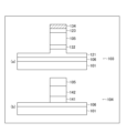
- FIG. 1A is a cross-sectional view showing a configuration of a semiconductor device according to an embodiment of the present invention.
- FIG. 1B is a cross-sectional view showing a partial configuration of a semiconductor device according to an embodiment of the present invention.
- FIG. 1C is a cross-sectional view showing a partial configuration of a semiconductor device according to an embodiment of the present invention.
- FIG. 1D is a cross-sectional view showing a partial configuration of a semiconductor device according to an embodiment of the present invention.
- FIG. 1A is a cross-sectional view showing a configuration of a semiconductor device according to an embodiment of the present invention.
- FIG. 1B is a cross-sectional view showing a partial configuration of a semiconductor device according to an embodiment of the present invention.
- FIG. 1C is a cross-sectional view showing a partial configuration of a semiconductor device according to an embodiment of the present invention.
- FIG. 1D is a cross-sectional view showing a partial configuration of a semiconductor device according to an
- FIG. 3A is a cross-sectional view showing a state of a semiconductor device in the middle of a process for explaining a method of manufacturing a semiconductor device according to an embodiment of the present invention.
- FIG. 3B is a cross-sectional view showing a state of the semiconductor device in the middle of a process for explaining a method of manufacturing a semiconductor device according to an embodiment of the present invention.
- FIG. 3C is a cross-sectional view showing a state of the semiconductor device in the middle of a process for explaining a method of manufacturing a semiconductor device according to an embodiment of the present invention.
- FIG. 3D is a cross-sectional view showing a state of the semiconductor device in the middle of a process for explaining a method of manufacturing a semiconductor device according to an embodiment of the present invention.
- FIG. 3E is a cross-sectional view showing a state of the semiconductor device in the middle of a process for explaining a method of manufacturing a semiconductor device according to an embodiment of the present invention.
- FIG. 3F is a cross-sectional view showing a state of the semiconductor device in the middle of a process for explaining a method of manufacturing a semiconductor device according to an embodiment of the present invention.
- FIG. 3D is a cross-sectional view showing a state of the semiconductor device in the middle of a process for explaining a method of manufacturing a semiconductor device according to an embodiment of the present invention.
- FIG. 3E is a cross-
- FIG. 3G is a cross-sectional view showing a state of a semiconductor device in the middle of a process for explaining a method of manufacturing a semiconductor device according to an embodiment of the present invention.
- FIG. 3H is a cross-sectional view showing a state of the semiconductor device in the middle of a process for explaining a method of manufacturing a semiconductor device according to an embodiment of the present invention.
- FIG. 3I is a cross-sectional view showing a state of a semiconductor device in the middle of a process for explaining a method of manufacturing a semiconductor device according to an embodiment of the present invention.
- FIG. 3J is a cross-sectional view showing a state of a semiconductor device in the middle of a process for explaining a method of manufacturing a semiconductor device according to an embodiment of the present invention.
- FIG. 3K is a cross-sectional view showing a state of a semiconductor device in the middle of a process for explaining a method of manufacturing a semiconductor device according to an embodiment of the present invention.
- FIG. 3L is a cross-sectional view showing a state of a semiconductor device in the middle of a process for explaining a method of manufacturing a semiconductor device according to an embodiment of the present invention.
- FIG. 3M is a cross-sectional view showing a state of a semiconductor device in the middle of a process for explaining a method of manufacturing a semiconductor device according to an embodiment of the present invention.
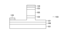
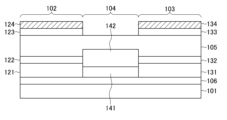
- This semiconductor device comprises a substrate 101 made of semi-insulating InP, a first optically active element 102 formed on the substrate 101, and a second optically active element 103 formed on the substrate 101. Between the first optically active element 102 and the second optically active element 103, there is provided an optical waveguide 104 which functions as an electrical separator between the first optically active element 102 and the second optically active element 103, and which optically connects the first optically active element 102 and the second optically active element 103.
- the substrate 101 can be made of InP that has been doped with Fe to give it high resistance.
- the substrate 101 can have the (001) plane of InP as its main surface.
- FIG. 1A shows a cross section parallel to the guiding direction of light as a carrier wave.
- FIGS. 11B, 1C, and 1D show cross sections perpendicular to the guiding direction.
- the first optically active element 102 includes a first lower semiconductor layer 121 made of n-type InP (e.g., doped at 1E18 cm -3 ) formed on a substrate 101, a first active layer 122 formed on the first lower semiconductor layer 121 to have a ridge-shaped waveguide structure, and an upper semiconductor layer 105 made of p-type InP formed on the first active layer 122.
- the first active layer 122 can be made of, for example, InGaAsP or InGaAlAs.
- the first active layer 122 can have a thickness of about 250 nm.
- the first optically active element 102 also includes a first p-electrode 124 formed on the upper semiconductor layer 105 and a first n-electrode 125 formed on the first lower semiconductor layer 121 in an area where the first active layer 122 is not formed.
- the first p-electrode 124 is formed on the upper semiconductor layer 105 via a contact layer 123.
- the contact layer 123 can be made of, for example, InGaAs doped with a high concentration of p-type impurities.
- the first optically active element 102 is a so-called vertical current injection type semiconductor laser that injects current into the first active layer 122 in a direction perpendicular to the plane of the substrate 101.
- the first optically active element 102 can be a distributed feedback (DFB) laser that includes a diffraction grating on the upper surface, lower surface, or side surface of the first active layer 122.
- the length of the first optically active element 102 in the waveguiding direction is the resonator length.
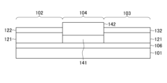
- the second optically active element 103 includes a second active layer 132 formed on the first lower semiconductor layer 121 and having a ridge-shaped waveguide structure, and an upper semiconductor layer 105 formed on the second active layer 132.
- the second active layer 132 can be made of, for example, InGaAsP or InGaAlAs.
- the second active layer 132 can have a thickness of about 280 nm.
- the second optically active element 103 also includes a second p-electrode 134 formed on the upper semiconductor layer 105, and a second n-electrode 135 formed on the first lower semiconductor layer 121 in an area where the second active layer 132 is not formed.
- the second p-electrode 134 is formed on the upper semiconductor layer 105 via the contact layer 123.
- the second optically active element 103 is an electroabsorption type optical modulator (EA modulator).
- the first active layer 122 and the second active layer 132 can be a multiple quantum well structure (MQW structure).
- the first active layer 122 and the second active layer 132 represent the part including the MQW structure and the optical confinement layers (SCH) above and below it, and also function as the core of the waveguide structure.
- the optical waveguide 104 comprises a second lower semiconductor layer 141 made of semi-insulating or undoped InP, a third active layer 142 formed on the second lower semiconductor layer 141 and having a ridge-shaped waveguide structure, and an upper semiconductor layer 105 formed on the third active layer 142.
- the second lower semiconductor layer 141 is formed in a groove formed in the first lower semiconductor layer 121 in the region of the optical waveguide 104 between the first optical active element 102 and the second optical active element 103.
- the upper semiconductor layer 105 is formed in common to the first optical active element 102, the second optical active element 103, and the optical waveguide 104.
- the third active layer 142 functions as the core of the optical waveguide 104.
- the second lower semiconductor layer 141 and the upper semiconductor layer 105 function as cladding.
- the third active layer 142 can be composed of, for example, InGaAsP with a composition ratio of 1.1 ⁇ m band gap wavelength.
- the device also includes an etching stop layer 106 formed over the entire surface of the substrate 101.
- the first optically active element 102, the optical waveguide 104, and the second optically active element 103 are formed on the etching stop layer 106.
- the etching stop layer 106 is made of a different material than the first lower semiconductor layer 121 and the second lower semiconductor layer 141.
- the first lower semiconductor layer 121 in the region where the second active layer 132 is not formed is formed thinner than the first lower semiconductor layer 121 in the region where the second active layer 132 is formed.
- a buried layer 107 is provided that is formed on the first lower semiconductor layer 121 and buries the first active layer 122.
- the buried layer 107 is composed of a p-type buried layer 107a and an n-type buried layer 107b.
- the buried layer 107 is not limited to this and can be composed of highly resistive semi-insulating InP.
- the first n-electrode 125 is formed in the area where the buried layer 107 has been removed, and the first lower semiconductor layer 121 in which the first n-electrode 125 is formed (in the area in which the first active layer 122 is not formed) has a thickness of 200 to 1000 nm. Furthermore, the first n-electrode 125 is formed 2 to 20 ⁇ m away from the first active layer 122.
- the resistivity ⁇ of n-type InP is 2.7E10 ⁇ 3 ( ⁇ cm) when the doping amount is 1E18 (cm ⁇ 3 ).
- the thickness of the first lower semiconductor layer 121 in the region where the first n-electrode 125 is formed is t ( ⁇ m)
- the length of the first optical active element 102 in the waveguiding direction is L ( ⁇ m).
- the distance between the first n-electrode 125 and the first active layer 122 is d ( ⁇ m).
- Figure 2 shows the calculation results of the resistance value R when the length L in the waveguide direction is 300 ⁇ m and the thickness t is 0.2, 0.5, and 0.8 ⁇ m.
- the thickness t of the first lower semiconductor layer 121 made of n-type InP is 0.2 ⁇ m (200 nm)
- the distance d is 20 ⁇ m or less (2 ⁇ m ⁇ d)
- a resistance value of 10 ⁇ or less that allows the first optical active element 102 to operate normally can be achieved.
- the first lower semiconductor layer 121 there is a limit to the thickness of the first lower semiconductor layer 121. If the first lower semiconductor layer 121 is made too thick, the following problems will occur. As is well known, in the semiconductor device according to the embodiment, when forming the buried layer 107, the first active layer 122 is patterned into a ridge shape (high mesa shape), and the buried layer 107 is grown by crystal regrowth on the first lower semiconductor layer 121 on both sides of this.
- the thickness of the first lower semiconductor layer 121 increases, a problem of abnormal growth occurs in which the thickness of the semiconductor layer growing at the regrowth interface increases abnormally.
- the resistance value of the first lower semiconductor layer 121 between the first n-electrode 125 and the first active layer 122 is about 1 ⁇ , according to the calculation results shown in FIG. 2.
- This value is sufficiently smaller than the comparison of the resistance of the LD on the SI substrate and the LD on the n substrate described in Non-Patent Document 1. In this way, according to the embodiment, it can be considered that the influence on the optical output characteristics of the first optical active element 102 can be suppressed.
- a 10 nm thick etching stop layer 106 is formed on the substrate 101 by crystal growth of undoped InGaAsP.
- an 800 nm thick InP layer 201 is formed by crystal growth of n-type InP (doping amount 1E18).
- an active layer 202 is formed (crystal growth) with a thickness of 250 nm from InGaAsP.
- the crystal growth of each semiconductor layer can be performed, for example, by the well-known metalorganic vapor phase epitaxy method. The crystal growth of each semiconductor layer shown below is similar.
- active layer 202 in the region that will become the second optically active element 103 is removed to form active layer 202a as shown in FIG. 3B, and active layer 202b of, for example, InGaAsP with a thickness of 280 nm is formed (crystal growth) in the removed area, and active layer 202a and active layer 202b are butt-jointed in the waveguiding direction (butt-joint process).
- active layer 202a and active layer 202b may have a multiple quantum well structure (MQW structure).
- MQW structure multiple quantum well structure
- the thickness is set as described above, including the optical confinement layers (SCH) above and below the MQW structure.
- predetermined regions of active layer 202a, active layer 202b, and InP layer 201 are removed by etching using a mask pattern (not shown) formed by known photolithography technology to form first lower semiconductor layer 121 and first active layer 122 of first optical active element 102, and first lower semiconductor layer 121 and second optical active element 103, as shown in FIG. 3C.
- the region of the first optical active element 102 and the second optical active element 103 is the region where the optical waveguide 104 is formed.
- selective wet etching using the etching stop layer 106 can be used.
- the etching stop layer 106 made of InGaAsP is not etched, and the layer made of InP can be selectively etched away.
- the second lower semiconductor layer 141 and the third active layer 142 of the optical waveguide 104 are formed by crystal growth.
- the second lower semiconductor layer 141 can be formed to a thickness of about 700 nm
- the third active layer 142 can be formed to a thickness of about 400 nm.
- a waveguide for the first optically active element 102 is formed by etching using a mask pattern (not shown) formed by known photolithography technology.
- the mask pattern is shaped to cover the entire area of the second optically active element 103 and the optical waveguide 104, and the area of the second optically active element 103 and the optical waveguide 104 is not patterned.
- the first lower semiconductor layer 121 is thinned on both sides of the ridge-shaped waveguide structure of the first active layer 122.
- the region where the first lower semiconductor layer 121 is thinned is the region where the first n-electrode 125 is formed, and as mentioned above, the thickness is thinned to a limit of 200 nm.
- the first optical active element 102 has an optical waveguide structure with the first active layer 122 as the core.
- a semiconductor layer doped with a high concentration of conductive impurities n-type impurities
- the first lower semiconductor layer 121 becomes a semiconductor layer doped with a high concentration of impurities. Therefore, if only the first active layer 122 is ridge-shaped, a semiconductor layer doped with a high concentration of impurities exists not only directly below the ridge-shaped first active layer 122 but also near both side surfaces.
- the semiconductor layer doped with a high concentration of impurities in the regions other than directly below the first active layer 122 can be separated from the first active layer 122, making it possible to suppress the waveguide loss.
- InP is crystal-regrown on the first lower semiconductor layer 121 remaining on both sides of the ridge-shaped waveguide structure, thereby burying the ridge-shaped waveguide structure with burying layer 107.
- a selective growth mask (not shown) made of silicon oxide or the like is first formed on the first active layer 122.
- p-type InP is regrown to form p-type burying layer 107a.
- n-type InP is grown to form n-type burying layer 107b, thereby forming burying layer 107 made up of p-type burying layer 107a and n-type burying layer 107b.
- the upper semiconductor layer 105 is formed by crystal growth of p-type InP, and then the contact layer 203 is formed by crystal growth of InGaAsP or InGaAs.
- the contact layer 203 in the region of the optical waveguide 104 is removed by etching using a mask pattern (not shown) formed by known photolithography technology, thereby forming contact layers 123 on the first optical active element 102 and on the second optical active element 103, as shown in FIG. 3I.
- the contact layer 123 on the first optical active element 102 and the contact layer 123 on the second optical active element 103 are formed to be electrically isolated from each other in a planar direction parallel to the surface of the upper semiconductor layer 105.
- a first p-electrode 124 is formed on the contact layer 123 above the first optically active element 102, and a second p-electrode 134 is formed on the contact layer 123 above the second optically active element 103.
- the second optically active element 103 and the optical waveguide 104 are patterned into a high mesa structure. Note that, similar to the region of the first optically active element 102 described above, in the second optically active element 103, the first lower semiconductor layer 121 on both sides of the high mesa waveguide structure is thinned.
- a first n-electrode 125 is formed to electrically connect to the first lower semiconductor layer 121 of the first optical active element 102, and a second n-electrode 135 is formed to electrically connect to the first lower semiconductor layer 121 of the second optical active element 103.
- the contact layer 123, the upper semiconductor layer 105, and the buried layer 107 in the region where the first n-electrode 125 is to be formed are patterned and removed by known lithography and etching techniques to expose the upper surface of the first lower semiconductor layer 121. Thereafter, the first n-electrode 125 is formed on the exposed upper surface of the first lower semiconductor layer 121.
- the region in which the first n-electrode of the first lower semiconductor layer made of n-type InP below the first active layer is formed has a thickness of 200 to 1000 nm, so that two monolithically integrated optical active elements can be driven in different ways without causing degradation of the optical output characteristics or optical modulation characteristics.
Landscapes
- Physics & Mathematics (AREA)
- Condensed Matter Physics & Semiconductors (AREA)
- General Physics & Mathematics (AREA)
- Electromagnetism (AREA)
- Optics & Photonics (AREA)
- Geometry (AREA)
- Semiconductor Lasers (AREA)
Priority Applications (2)
| Application Number | Priority Date | Filing Date | Title |
|---|---|---|---|
| PCT/JP2022/041677 WO2024100788A1 (ja) | 2022-11-09 | 2022-11-09 | 半導体装置 |
| JP2024556907A JPWO2024100788A1 (https=) | 2022-11-09 | 2022-11-09 |
Applications Claiming Priority (1)
| Application Number | Priority Date | Filing Date | Title |
|---|---|---|---|
| PCT/JP2022/041677 WO2024100788A1 (ja) | 2022-11-09 | 2022-11-09 | 半導体装置 |
Publications (1)
| Publication Number | Publication Date |
|---|---|
| WO2024100788A1 true WO2024100788A1 (ja) | 2024-05-16 |
Family
ID=91032505
Family Applications (1)
| Application Number | Title | Priority Date | Filing Date |
|---|---|---|---|
| PCT/JP2022/041677 Ceased WO2024100788A1 (ja) | 2022-11-09 | 2022-11-09 | 半導体装置 |
Country Status (2)
| Country | Link |
|---|---|
| JP (1) | JPWO2024100788A1 (https=) |
| WO (1) | WO2024100788A1 (https=) |
Citations (5)
| Publication number | Priority date | Publication date | Assignee | Title |
|---|---|---|---|---|
| JP2010157691A (ja) * | 2008-12-02 | 2010-07-15 | Opnext Japan Inc | 光半導体装置 |
| JP2011009456A (ja) * | 2009-06-25 | 2011-01-13 | Opnext Japan Inc | 半導体光素子、及びその製造方法 |
| JP2015072980A (ja) * | 2013-10-02 | 2015-04-16 | 富士通株式会社 | 光半導体素子、光半導体素子アレイ、光送信モジュール及び光伝送システム |
| JP2017003729A (ja) * | 2015-06-09 | 2017-01-05 | 日本オクラロ株式会社 | 光信号生成装置 |
| US20190326729A1 (en) * | 2016-11-17 | 2019-10-24 | Fraunhofer-Gesellschaft zur Förderung der angewandten Forschung e.V. | Method for fabricating an elctro-absorption modulated laser and electro-absorption modulated laser |
-
2022
- 2022-11-09 JP JP2024556907A patent/JPWO2024100788A1/ja active Pending
- 2022-11-09 WO PCT/JP2022/041677 patent/WO2024100788A1/ja not_active Ceased
Patent Citations (5)
| Publication number | Priority date | Publication date | Assignee | Title |
|---|---|---|---|---|
| JP2010157691A (ja) * | 2008-12-02 | 2010-07-15 | Opnext Japan Inc | 光半導体装置 |
| JP2011009456A (ja) * | 2009-06-25 | 2011-01-13 | Opnext Japan Inc | 半導体光素子、及びその製造方法 |
| JP2015072980A (ja) * | 2013-10-02 | 2015-04-16 | 富士通株式会社 | 光半導体素子、光半導体素子アレイ、光送信モジュール及び光伝送システム |
| JP2017003729A (ja) * | 2015-06-09 | 2017-01-05 | 日本オクラロ株式会社 | 光信号生成装置 |
| US20190326729A1 (en) * | 2016-11-17 | 2019-10-24 | Fraunhofer-Gesellschaft zur Förderung der angewandten Forschung e.V. | Method for fabricating an elctro-absorption modulated laser and electro-absorption modulated laser |
Also Published As
| Publication number | Publication date |
|---|---|
| JPWO2024100788A1 (https=) | 2024-05-16 |
Similar Documents
| Publication | Publication Date | Title |
|---|---|---|
| US6455338B1 (en) | Method of manufacturing an integrated semiconductor laser-modulator device | |
| US8384980B2 (en) | Semiconductor optical modulation device, Mach-Zehnder interferometer type semiconductor optical modulator, and method for producing semiconductor optical modulation device | |
| JP2019054107A (ja) | 半導体光素子 | |
| JP4690515B2 (ja) | 光変調器、半導体光素子、及びそれらの作製方法 | |
| JP4909159B2 (ja) | 半導体導波路素子およびその作製方法ならびに半導体レーザ | |
| US20210184421A1 (en) | Semiconductor Optical Element | |
| JP3752369B2 (ja) | 複合光デバイスの製造方法 | |
| US6931041B2 (en) | Integrated semiconductor laser device and method of manufacture thereof | |
| JP2882335B2 (ja) | 光半導体装置およびその製造方法 | |
| US6602432B2 (en) | Electroabsorption modulator, and fabricating method of the same | |
| JP2011077329A (ja) | 半導体光集積素子、及びその製造方法 | |
| JP4947778B2 (ja) | 光半導体素子及びその製造方法 | |
| JP4014861B2 (ja) | 化合物半導体デバイス及びその作製方法 | |
| US20250379417A1 (en) | Semiconductor device | |
| WO2024100788A1 (ja) | 半導体装置 | |
| WO2024236631A1 (ja) | 半導体装置 | |
| JP4105618B2 (ja) | 半導体光変調導波路 | |
| JPH06112595A (ja) | 半導体光機能素子の製造方法 | |
| US20250219352A1 (en) | Semiconductor device | |
| JP5109931B2 (ja) | 半導体光集積素子および半導体光集積素子の製造方法 | |
| US6937632B2 (en) | Integrated semiconductor laser and waveguide device | |
| JP4161672B2 (ja) | 光集積素子の製造方法 | |
| JP3146821B2 (ja) | 半導体光集積素子の製造方法 | |
| JP4164248B2 (ja) | 半導体素子及びその製造方法、及び半導体光装置 | |
| JP4283079B2 (ja) | 半導体光電子導波路 |
Legal Events
| Date | Code | Title | Description |
|---|---|---|---|
| 121 | Ep: the epo has been informed by wipo that ep was designated in this application |
Ref document number: 22965113 Country of ref document: EP Kind code of ref document: A1 |
|
| WWE | Wipo information: entry into national phase |
Ref document number: 2024556907 Country of ref document: JP |
|
| NENP | Non-entry into the national phase |
Ref country code: DE |
|
| 122 | Ep: pct application non-entry in european phase |
Ref document number: 22965113 Country of ref document: EP Kind code of ref document: A1 |