WO2024070477A1 - 出力電位切替回路 - Google Patents
出力電位切替回路 Download PDFInfo
- Publication number
- WO2024070477A1 WO2024070477A1 PCT/JP2023/031831 JP2023031831W WO2024070477A1 WO 2024070477 A1 WO2024070477 A1 WO 2024070477A1 JP 2023031831 W JP2023031831 W JP 2023031831W WO 2024070477 A1 WO2024070477 A1 WO 2024070477A1
- Authority
- WO
- WIPO (PCT)
- Prior art keywords
- terminal
- power card
- semiconductor module
- switching element
- potential
- Prior art date
- Legal status (The legal status is an assumption and is not a legal conclusion. Google has not performed a legal analysis and makes no representation as to the accuracy of the status listed.)
- Ceased
Links
Images









Classifications
-
- H—ELECTRICITY
- H02—GENERATION; CONVERSION OR DISTRIBUTION OF ELECTRIC POWER
- H02M—APPARATUS FOR CONVERSION BETWEEN AC AND AC, BETWEEN AC AND DC, OR BETWEEN DC AND DC, AND FOR USE WITH MAINS OR SIMILAR POWER SUPPLY SYSTEMS; CONVERSION OF DC OR AC INPUT POWER INTO SURGE OUTPUT POWER; CONTROL OR REGULATION THEREOF
- H02M7/00—Conversion of AC power input into DC power output; Conversion of DC power input into AC power output
- H02M7/42—Conversion of DC power input into AC power output without possibility of reversal
- H02M7/44—Conversion of DC power input into AC power output without possibility of reversal by static converters
- H02M7/48—Conversion of DC power input into AC power output without possibility of reversal by static converters using discharge tubes with control electrode or semiconductor devices with control electrode
- H02M7/483—Converters with outputs that each can have more than two voltages levels
-
- H—ELECTRICITY
- H02—GENERATION; CONVERSION OR DISTRIBUTION OF ELECTRIC POWER
- H02M—APPARATUS FOR CONVERSION BETWEEN AC AND AC, BETWEEN AC AND DC, OR BETWEEN DC AND DC, AND FOR USE WITH MAINS OR SIMILAR POWER SUPPLY SYSTEMS; CONVERSION OF DC OR AC INPUT POWER INTO SURGE OUTPUT POWER; CONTROL OR REGULATION THEREOF
- H02M7/00—Conversion of AC power input into DC power output; Conversion of DC power input into AC power output
- H02M7/42—Conversion of DC power input into AC power output without possibility of reversal
- H02M7/44—Conversion of DC power input into AC power output without possibility of reversal by static converters
- H02M7/48—Conversion of DC power input into AC power output without possibility of reversal by static converters using discharge tubes with control electrode or semiconductor devices with control electrode
- H02M7/483—Converters with outputs that each can have more than two voltages levels
- H02M7/487—Neutral point clamped inverters
-
- H—ELECTRICITY
- H02—GENERATION; CONVERSION OR DISTRIBUTION OF ELECTRIC POWER
- H02M—APPARATUS FOR CONVERSION BETWEEN AC AND AC, BETWEEN AC AND DC, OR BETWEEN DC AND DC, AND FOR USE WITH MAINS OR SIMILAR POWER SUPPLY SYSTEMS; CONVERSION OF DC OR AC INPUT POWER INTO SURGE OUTPUT POWER; CONTROL OR REGULATION THEREOF
- H02M7/00—Conversion of AC power input into DC power output; Conversion of DC power input into AC power output
- H02M7/003—Constructional details, e.g. physical layout, assembly, wiring or busbar connections
-
- H—ELECTRICITY
- H02—GENERATION; CONVERSION OR DISTRIBUTION OF ELECTRIC POWER
- H02M—APPARATUS FOR CONVERSION BETWEEN AC AND AC, BETWEEN AC AND DC, OR BETWEEN DC AND DC, AND FOR USE WITH MAINS OR SIMILAR POWER SUPPLY SYSTEMS; CONVERSION OF DC OR AC INPUT POWER INTO SURGE OUTPUT POWER; CONTROL OR REGULATION THEREOF
- H02M7/00—Conversion of AC power input into DC power output; Conversion of DC power input into AC power output
- H02M7/42—Conversion of DC power input into AC power output without possibility of reversal
- H02M7/44—Conversion of DC power input into AC power output without possibility of reversal by static converters
- H02M7/48—Conversion of DC power input into AC power output without possibility of reversal by static converters using discharge tubes with control electrode or semiconductor devices with control electrode
-
- H—ELECTRICITY
- H02—GENERATION; CONVERSION OR DISTRIBUTION OF ELECTRIC POWER
- H02M—APPARATUS FOR CONVERSION BETWEEN AC AND AC, BETWEEN AC AND DC, OR BETWEEN DC AND DC, AND FOR USE WITH MAINS OR SIMILAR POWER SUPPLY SYSTEMS; CONVERSION OF DC OR AC INPUT POWER INTO SURGE OUTPUT POWER; CONTROL OR REGULATION THEREOF
- H02M7/00—Conversion of AC power input into DC power output; Conversion of DC power input into AC power output
- H02M7/42—Conversion of DC power input into AC power output without possibility of reversal
- H02M7/44—Conversion of DC power input into AC power output without possibility of reversal by static converters
- H02M7/48—Conversion of DC power input into AC power output without possibility of reversal by static converters using discharge tubes with control electrode or semiconductor devices with control electrode
- H02M7/53—Conversion of DC power input into AC power output without possibility of reversal by static converters using discharge tubes with control electrode or semiconductor devices with control electrode using devices of a triode or transistor type requiring continuous application of a control signal
- H02M7/537—Conversion of DC power input into AC power output without possibility of reversal by static converters using discharge tubes with control electrode or semiconductor devices with control electrode using devices of a triode or transistor type requiring continuous application of a control signal using semiconductor devices only, e.g. single switched pulse inverters
-
- H—ELECTRICITY
- H02—GENERATION; CONVERSION OR DISTRIBUTION OF ELECTRIC POWER
- H02M—APPARATUS FOR CONVERSION BETWEEN AC AND AC, BETWEEN AC AND DC, OR BETWEEN DC AND DC, AND FOR USE WITH MAINS OR SIMILAR POWER SUPPLY SYSTEMS; CONVERSION OF DC OR AC INPUT POWER INTO SURGE OUTPUT POWER; CONTROL OR REGULATION THEREOF
- H02M7/00—Conversion of AC power input into DC power output; Conversion of DC power input into AC power output
- H02M7/42—Conversion of DC power input into AC power output without possibility of reversal
- H02M7/44—Conversion of DC power input into AC power output without possibility of reversal by static converters
- H02M7/48—Conversion of DC power input into AC power output without possibility of reversal by static converters using discharge tubes with control electrode or semiconductor devices with control electrode
- H02M7/53—Conversion of DC power input into AC power output without possibility of reversal by static converters using discharge tubes with control electrode or semiconductor devices with control electrode using devices of a triode or transistor type requiring continuous application of a control signal
- H02M7/537—Conversion of DC power input into AC power output without possibility of reversal by static converters using discharge tubes with control electrode or semiconductor devices with control electrode using devices of a triode or transistor type requiring continuous application of a control signal using semiconductor devices only, e.g. single switched pulse inverters
- H02M7/5387—Conversion of DC power input into AC power output without possibility of reversal by static converters using discharge tubes with control electrode or semiconductor devices with control electrode using devices of a triode or transistor type requiring continuous application of a control signal using semiconductor devices only, e.g. single switched pulse inverters in a bridge configuration
Definitions
- This disclosure relates to an output potential switching circuit that is applied to a multilevel inverter.
- the present disclosure has been made to solve the above problems, and its main objective is to configure an output potential switching circuit that is applied to a multilevel inverter using a general-purpose semiconductor module.
- the first means for solving the above problem is to 1.
- An output potential switching circuit that is applied to a multilevel inverter, receives a multilevel potential, and switches an output potential to one of the multilevel potentials, a first switching element having a first diode connected in anti-parallel, a second switching element having a second diode connected in anti-parallel, a P terminal to which a positive terminal of the first switching element is connected, an O terminal to which a negative terminal of the first switching element and a positive terminal of the second switching element are connected, and an N terminal to which a negative terminal of the second switching element is connected,
- the P terminal of one of the semiconductor modules is connected to the O terminal of the other of the semiconductor modules.
- the output potential switching circuit is applied to a multilevel inverter, inputs multilevel potentials, and switches the output potential to one of the multilevel potentials.
- the output potential switching circuit includes a first switching element with a first diode connected in anti-parallel, a second switching element with a second diode connected in anti-parallel, a P terminal to which the positive terminal of the first switching element is connected, an O terminal to which the negative terminal of the first switching element and the positive terminal of the second switching element are connected, and an N terminal to which the negative terminal of the second switching element is connected (hereinafter referred to as "general-purpose semiconductor modules").
- the general-purpose semiconductor module is a semiconductor module that is used for general purposes such as a three-phase two-level inverter and constitutes a circuit for one phase.
- the P terminal of one of the semiconductor modules (hereinafter referred to as the "first semiconductor module”) is connected to the O terminal of the other one of the semiconductor modules (hereinafter referred to as the "second semiconductor module").
- the output potential output from the O terminal of the first semiconductor module can be switched to any one of the positive potential, neutral potential, and negative potential by inputting a positive potential to the P terminal of the second semiconductor module, inputting a neutral potential to the N terminal of the second semiconductor module, and inputting a negative potential to the N terminal of the first semiconductor module, and operating the switching elements of the first and second semiconductor modules. Therefore, an output potential switching circuit applicable to a multilevel inverter can be configured using general-purpose semiconductor modules.
- an output potential switching circuit applicable to a four-level inverter can be configured by inputting a positive potential to the P terminal of the third semiconductor module, a first intermediate potential to the N terminal of the third semiconductor module, a second intermediate potential to the N terminal of the second semiconductor module, and a negative potential to the N terminal of the first semiconductor module.
- an output potential switching circuit applicable to an inverter of five or more levels can also be configured by adding further general-purpose semiconductor modules.
- the semiconductor module is formed in a plate shape, and the P terminal, the N terminal, and the O terminal are arranged in this order at the end of the semiconductor module in a predetermined direction, and the one semiconductor module and the other one of the semiconductor modules are arranged in an inverted front-back stacked manner in the plate thickness direction so that the P terminal of the one semiconductor module faces the O terminal of the other one of the semiconductor modules.
- the P terminal of the one semiconductor module faces the O terminal of the other one of the semiconductor modules, making it easier to connect the P terminal of the one semiconductor module and the O terminal of the other one of the semiconductor modules. Furthermore, the direction of current flowing through the P terminal of the one semiconductor module is opposite to the direction of current flowing through the O terminal of the other one of the semiconductor modules, reducing the inductance of these terminals and reducing losses. Moreover, since the one semiconductor module and the other one of the semiconductor modules are stacked in the thickness direction with the front and back facing in opposite directions, the arrangement space for multiple semiconductor modules can be reduced.
- the semiconductor module is formed in a plate shape, and the P terminal, the N terminal, and the O terminal are arranged in this order at the end of the semiconductor module in a predetermined direction, and the one semiconductor module and the other one of the semiconductor modules are arranged side by side in the plate thickness direction with the front and back facing the same direction so that the P terminal of the one semiconductor module faces the O terminal of the other one of the semiconductor modules.
- the P terminal of the one semiconductor module faces the O terminal of the other one of the semiconductor modules, making it easier to connect the P terminal of the one semiconductor module to the O terminal of the other one of the semiconductor modules. Furthermore, the direction in which current flows through the P terminal of the one semiconductor module is opposite to the direction in which current flows through the O terminal of the other one of the semiconductor modules, reducing the inductance of these terminals and reducing losses.
- the semiconductor module is formed in a plate shape, and the P terminal, the N terminal, and the O terminal are arranged in this order at an end of the semiconductor module in a predetermined direction, and the one semiconductor module and the other one of the semiconductor modules are arranged in the same direction on the front and back, with the P terminal, the N terminal, and the O terminal arranged in the arrangement direction, so that the P terminal of the one semiconductor module and the O terminal of the other one of the semiconductor modules are adjacent to each other.
- the P terminal of the one of the semiconductor modules and the O terminal of the other one of the semiconductor modules are adjacent to each other, it is easy to connect the P terminal of the one of the semiconductor modules and the O terminal of the other one of the semiconductor modules. Furthermore, since the direction of current flowing through the P terminal of the one of the semiconductor modules is opposite to the direction of current flowing through the O terminal of the other one of the semiconductor modules, the inductance of these terminals can be reduced, thereby reducing losses.
- the semiconductor module is formed in a plate shape, and the P terminal, the O terminal, and the N terminal are arranged in this order at the end of the semiconductor module in a predetermined direction, and the one semiconductor module and the other one of the semiconductor modules are arranged side by side in the plate thickness direction with the front and back facing the same or opposite sides so that the P terminal of the one semiconductor module faces the O terminal of the other one of the semiconductor modules.
- the P terminal of the one semiconductor module faces the O terminal of the other one of the semiconductor modules, making it easier to connect the P terminal of the one semiconductor module to the O terminal of the other one of the semiconductor modules. Furthermore, the direction in which current flows through the P terminal of the one semiconductor module is opposite to the direction in which current flows through the O terminal of the other one of the semiconductor modules, reducing the inductance of these terminals and reducing losses.
- a configuration can be adopted in which the O terminal of the semiconductor module, to which the lowest potential of the multi-level potentials is input to the N terminal, is connected to one phase coil of a rotating electric machine, and a potential of the multi-level potentials higher than the potential input to the N terminal of the one semiconductor module is input to the N terminal of the other one of the semiconductor modules.
- one output potential switching circuit is associated with one phase coil of the rotating electric machine, and the potential output to one phase coil of the rotating electric machine can be switched to a multi-level potential.
- the seventh means is 1.
- An output potential switching circuit that is applied to a multilevel inverter, receives a multilevel potential, and switches an output potential to one of the multilevel potentials, a first switching element having a first diode connected in anti-parallel, a second switching element having a second diode connected in anti-parallel, a P terminal to which a positive terminal of the first switching element is connected, an O terminal to which a negative terminal of the first switching element and a positive terminal of the second switching element are connected, and an N terminal to which a negative terminal of the second switching element is connected, The N terminal of one of the semiconductor modules is connected to the O terminal of the other of the semiconductor modules.
- the output potential switching circuit includes a plurality of general-purpose semiconductor modules.
- the N terminal of one of the semiconductor modules (hereinafter referred to as the "first semiconductor module”) is connected to the O terminal of the other one of the semiconductor modules (hereinafter referred to as the "second semiconductor module").
- the output potential switching circuit when the output potential switching circuit is composed of only the first semiconductor module and the second semiconductor module, the output potential output from the O terminal of the first semiconductor module can be switched to any one of the positive potential, neutral potential, and negative potential by inputting a positive potential to the P terminal of the first semiconductor module, inputting a neutral potential to the P terminal of the second semiconductor module, and inputting a negative potential to the N terminal of the second semiconductor module, and operating the switching elements of the first and second semiconductor modules. Therefore, an output potential switching circuit applied to a multilevel inverter can be configured using general-purpose semiconductor modules.
- an output potential switching circuit applicable to a four-level inverter can be configured by inputting a positive potential to the P terminal of the first semiconductor module, a first intermediate potential to the P terminal of the second semiconductor module, a second intermediate potential to the P terminal of the third semiconductor module, and a negative potential to the N terminal of the third semiconductor module.
- an output potential switching circuit applicable to an inverter of five or more levels can also be configured by adding further general-purpose semiconductor modules.
- the semiconductor module is formed in a plate shape, and the N terminal, the P terminal, and the O terminal are arranged in this order at the end of the semiconductor module in a predetermined direction, and the one semiconductor module and the other one of the semiconductor modules are arranged in an inverted front-back stacked manner in the plate thickness direction so that the N terminal of the one semiconductor module faces the O terminal of the other one of the semiconductor modules.
- the N terminal of the one semiconductor module faces the O terminal of the other one of the semiconductor modules, making it easier to connect the N terminal of the one semiconductor module and the O terminal of the other one of the semiconductor modules. Furthermore, the direction of current flowing through the N terminal of the one semiconductor module is opposite to the direction of current flowing through the O terminal of the other one of the semiconductor modules, reducing the inductance of these terminals and reducing losses. Moreover, since the one semiconductor module and the other one of the semiconductor modules are stacked in the thickness direction with the front and back facing in opposite directions, the arrangement space for multiple semiconductor modules can be reduced.
- the semiconductor module is formed in a plate shape, and the N terminal, the P terminal, and the O terminal are arranged in this order at an end of the semiconductor module in a predetermined direction, and the one semiconductor module and the other one of the semiconductor modules are arranged side by side in the plate thickness direction with the front and back facing the same direction so that the N terminal of the one semiconductor module faces the O terminal of the other one of the semiconductor modules.
- the N terminal of the one semiconductor module faces the O terminal of the other one of the semiconductor modules, making it easier to connect the N terminal of the one semiconductor module to the O terminal of the other one of the semiconductor modules. Furthermore, the direction in which current flows through the N terminal of the one semiconductor module is opposite to the direction in which current flows through the O terminal of the other one of the semiconductor modules, reducing the inductance of these terminals and reducing losses.
- the semiconductor module is formed in a plate shape, and the N terminal, the P terminal, and the O terminal are arranged in this order at an end of the semiconductor module in a predetermined direction, and the one semiconductor module and the other one of the semiconductor modules are arranged in the same direction on the front and back, so that the N terminal of the one semiconductor module and the O terminal of the other one of the semiconductor modules are adjacent to each other, and the one semiconductor module and the other one of the semiconductor modules are arranged in the same direction in the arrangement of the N terminal, the P terminal, and the O terminal.
- the N terminal of the one semiconductor module and the O terminal of the other one of the semiconductor modules are adjacent to each other, making it easier to connect the N terminal of the one semiconductor module and the O terminal of the other one of the semiconductor modules. Furthermore, the direction in which current flows through the N terminal of the one semiconductor module is opposite to the direction in which current flows through the O terminal of the other one of the semiconductor modules, reducing the inductance of these terminals and reducing losses.
- the semiconductor module is formed in a plate shape, and the P terminal, the O terminal, and the N terminal are arranged in this order at the end of the semiconductor module in a predetermined direction, and the one semiconductor module and the other one of the semiconductor modules are arranged side by side in the plate thickness direction with the front and back facing the same or opposite directions so that the N terminal of the one semiconductor module faces the O terminal of the other one of the semiconductor modules.
- the N terminal of the one semiconductor module faces the O terminal of the other one of the semiconductor modules, making it easier to connect the N terminal of the one semiconductor module to the O terminal of the other one of the semiconductor modules. Furthermore, the direction in which current flows through the N terminal of the one semiconductor module is opposite to the direction in which current flows through the O terminal of the other one of the semiconductor modules, reducing the inductance of these terminals and reducing losses.
- a configuration can be adopted in which the O terminal of the semiconductor module, to which the highest potential of the multi-level potentials is input to the P terminal, is connected to one phase coil of a rotating electric machine, and a potential of the multi-level potentials lower than the potential input to the P terminal of the one semiconductor module is input to the P terminal of the other one of the semiconductor modules.
- one output potential switching circuit is associated with one phase coil of the rotating electric machine, and the potential output to one phase coil of the rotating electric machine can be switched to a multi-level potential.
- the thirteenth means is 1.
- An output potential switching circuit that is applied to a multilevel inverter, receives a multilevel potential, and switches an output potential to one of the multilevel potentials, a first switching element having a first diode connected in anti-parallel, a second switching element having a second diode connected in anti-parallel, a P terminal to which a positive terminal of the first switching element is connected, an O terminal to which a negative terminal of the first switching element and a positive terminal of the second switching element are connected, and an N terminal to which a negative terminal of the second switching element is connected,
- the first diode, the first switching element, the second diode, and the second switching element are the only elements included, and no other elements are included.
- the output potential switching circuit includes a plurality of general-purpose semiconductor modules, as in the first means.
- the first semiconductor module by connecting the P terminal of one of the semiconductor modules (hereinafter referred to as the "first semiconductor module") to the O terminal of another of the semiconductor modules (hereinafter referred to as the "second semiconductor module"), the same effect as the first means can be achieved.
- the N terminal of the first semiconductor module by connecting the N terminal of the first semiconductor module to the O terminal of the second semiconductor module, the same effect as the seventh means can be achieved.
- the output potential switching circuit includes only the first diode, the first switching element, the second diode, and the second switching element as elements, and does not include any other elements. Therefore, the output potential switching circuit can be configured without requiring any elements other than those included in the general-purpose semiconductor modules.
- FIG. 1 is a schematic diagram showing a circuit configuration of a power card
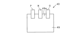
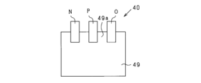
- FIG. 2 is a schematic diagram showing the front of a power card
- FIG. 3 is a schematic diagram showing the top surface of a power card
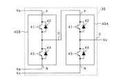
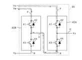
- FIG. 4 is a circuit diagram showing an output potential switching circuit applied to the three-level inverter of the first embodiment
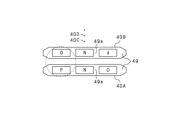
- FIG. 5 is a plan view showing the arrangement of the power cards
- FIG. 6 is a circuit diagram showing an output potential switching circuit and its peripheral configuration according to a first embodiment
- FIG. 7 is a circuit diagram showing a current flow when a switching element is switched
- FIG. 1 is a schematic diagram showing a circuit configuration of a power card
- FIG. 2 is a schematic diagram showing the front of a power card
- FIG. 3 is a schematic diagram showing the top surface of a power card
- FIG. 4 is a circuit diagram showing an output potential switching circuit applied to the three-level inverter of the first embodiment
- FIG. 5 is a plan view showing the arrangement of the power cards
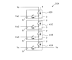
- FIG. 8 is a circuit diagram showing an output potential switching circuit applied to a five-level inverter;
- FIG. 9 is a plan view showing a modified example of the arrangement of the power cards;
- FIG. 10 is a plan view showing another modified example of the arrangement of the power cards;
- FIG. 11 is a schematic diagram showing a front view of a modified example of the power card;
- FIG. 12 is a plan view showing another modified example of the arrangement of the power cards;
- FIG. 13 is a circuit diagram showing an output potential switching circuit applied to a three-level inverter according to a second embodiment;
- FIG. 14 is a schematic diagram showing the front of the power card;
- FIG. 15 is a plan view showing the arrangement of the power cards;
- FIG. 15 is a plan view showing the arrangement of the power cards;
- FIG. 16 is a circuit diagram showing an output potential switching circuit and its peripheral configuration according to a second embodiment
- FIG. 17 is a circuit diagram showing a current flow when a switching element is switched
- FIG. 18 is a circuit diagram showing an output potential switching circuit applied to a five-level inverter.
- FIG. 19 is a plan view showing a modified example of the arrangement of the power cards
- FIG. 20 is a plan view showing another modification of the arrangement of the power cards
- FIG. 21 is a plan view showing another modification of the arrangement of the power cards
- FIG. 22 is a schematic diagram showing a modified example of the circuit configuration of the power card
- FIG. 23 is a circuit diagram showing a conventional three-level inverter and its peripheral configuration.
- a first embodiment of the present invention will be described with reference to the drawings, which is embodied in an output potential switching circuit applied to a three-level inverter (multilevel inverter) that converts power between a direct current power supply and a rotating electric machine mounted on a vehicle.
- the vehicle is an electric vehicle, a hybrid vehicle, etc.
- the rotating electric machine is a motor, a generator, a motor generator (MG), etc.
- Figure 23 is a circuit diagram showing a conventional three-level inverter and its peripheral configuration.
- the voltage Vh of the battery 11 is divided by the capacitors C1 and C2 into voltages of Vh/2 each and supplied to the inverter 120.
- the capacitors C1 and C2 function as a DC power supply 13 that outputs three levels of potential.
- the potential on the positive electrode side of the capacitor C1 is the positive electrode potential Vp
- the potential on the negative electrode side of the capacitor C2 is the negative electrode potential Vn
- the potential at the connection point (neutral point M) between the negative electrode side of the capacitor C1 and the positive electrode side of the capacitor C2 is the neutral point potential Vm.
- the U-phase series-connected circuit 160 is composed of a series-connected circuit of an upper arm made of MOSFET 111 with diode 112 connected in reverse parallel, and a lower arm made of MOSFET 113 with diode 114 connected in reverse parallel.
- the V-phase series-connected circuit 161 is composed of a series-connected circuit of an upper arm made of MOSFET 121 with diode 122 connected in reverse parallel, and a lower arm made of MOSFET 123 with diode 124 connected in reverse parallel.
- the W-phase series-connected circuit 162 is composed of a series-connected circuit of an upper arm made of MOSFET 131 with diode 132 connected in reverse parallel, and a lower arm made of MOSFET 133 with diode 134 connected in reverse parallel.
- AC switches having MOSFETs connected in anti-series with diodes connected in anti-parallel are connected between the series connection point of the upper and lower arms of the series connection circuit of each phase and the neutral point potential Vm. That is, AC switch circuit 163 having a configuration in which the source of MOSFET 181 with diode 182 connected in anti-parallel and the source of MOSFET 183 with diode 184 connected in anti-parallel are connected between the series connection point of series connection circuit 160 for U phase and neutral point M of DC power supply 13 are connected.
- AC switch circuit 164 having a configuration in which the source of MOSFET 185 with diode 186 connected in anti-parallel and the source of MOSFET 187 with diode 188 connected in anti-parallel are connected between the series connection point of series connection circuit 161 for V phase and neutral point M of DC power supply 13 are connected.
- an AC switch circuit 165 is connected in which the source of a MOSFET 189 with a diode 190 connected in anti-parallel and the source of a MOSFET 191 with a diode 192 connected in anti-parallel are connected.
- the series connection points of the series connection circuits 160, 161, and 162 are AC outputs and are connected to the coils 12u, 12v, and 12w of each phase of the rotating electric machine 12.
- the series connection points of each of the series connection circuits 160, 161, and 162 can output a positive electrode potential Vp, a negative electrode potential Vn, and a neutral point potential Vm, resulting in a three-level inverter output.
- one phase circuit 170 which is composed of a W-phase series connection circuit 162 and an AC switch circuit 165, is composed of two power cards.
- the power card (general-purpose semiconductor module, semiconductor module) is a semiconductor module that is general-purpose for three-phase two-level inverters and the like, and composes one phase of the circuit.
- FIG. 1 is a schematic diagram showing the circuit configuration of a power card 40.
- the power card 40 (2-in-1 module) includes a first switching element 41, a first diode 42, a second switching element 43, a second diode 44, a P terminal, an O terminal, an N terminal, and molded resin 49.
- the first switching element 41 is a semiconductor element such as an IGBT (Insulated Gate Bipolar Transistor) or a MOSFET (Metal-Oxide-Semiconductor Field-Effect Transistor).
- IGBT Insulated Gate Bipolar Transistor
- MOSFET Metal-Oxide-Semiconductor Field-Effect Transistor
- the collector (positive terminal) of the first switching element 41 is connected to the P terminal.
- the emitter (negative terminal) of the first switching element 41 is connected to the collector (positive terminal) of the second switching element 43.
- the emitter of the first switching element 41 and the collector of the second switching element 43 are connected to the O terminal. That is, the series connection point 45 between the first switching element 41 and the second switching element 43 is connected to the O terminal.
- the emitter (negative terminal) of the second switching element 43 is connected to the N terminal.
- the first switching element 41, the first diode 42, the second switching element 43, and the second diode 44 are sealed with a molded resin 49 (sealing resin).
- FIG. 2 is a schematic diagram showing the front of the power card 40
- FIG. 3 is a schematic diagram showing the top of the power card 40.
- the molded resin 49 (power card 40) is formed in a rectangular plate shape (plate shape).
- the P terminal, N terminal, and O terminal are arranged in this order at an end 49a (end in a specific direction) along one long side of the molded resin 49 (power card 40).
- the P terminal, N terminal, and O terminal are formed in a rectangular plate shape (plate shape, rod shape) from a metal alloy (conductor).
- the P terminal, N terminal, and O terminal are exposed to the outside from the molded resin 49.
- the P terminal and O terminal are respectively arranged at both ends (near both ends) in the longitudinal direction of the molded resin 49.
- the N terminal is arranged in the center (near the center) of the longitudinal direction of the molded resin 49.
- FIG. 4 is a circuit diagram showing the output potential switching circuit 30.
- the output potential switching circuit 30 is a circuit equivalent to the one-phase circuit 170 composed of the series connection circuit 162 and the AC switch circuit 165 in FIG. 23.
- the output potential switching circuit 30 includes a first power card 40A and a second power card 40B as the power cards 40.
- the output potential switching circuit 30 includes only the first diode 42, the first switching element 41, the second diode 44, and the second switching element 43, i.e., only the elements included in each power card 40A, 40B, and does not include any other elements.
- the P terminal of the first power card 40A (first semiconductor module, one semiconductor module) is connected to the O terminal of the second power card 40B (second semiconductor module, another semiconductor module).
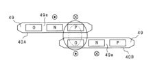
- the first power card 40A and the second power card 40B are arranged in the thickness direction with the front and back facing in the opposite directions so that the P terminal of the first power card 40A faces the O terminal of the second power card 40B.
- the first power card 40A and the second power card 40B are arranged adjacent to each other with the front and back facing in the opposite directions, with the ends 49a on which the terminals are arranged facing the same direction.
- the outer edge of the first power card 40A and the outer edge of the second power card 40B are aligned.
- the P terminal of the first power card 40A and the O terminal of the second power card 40B are connected.
- the N terminal of the first power card 40A and the N terminal of the second power card 40B face each other, and the O terminal of the first power card 40A and the P terminal of the second power card 40B face each other.
- FIG. 6 is a circuit diagram showing the output potential switching circuit 30 and its peripheral configuration. Note that parts that are the same as those in FIG. 23 are given the same reference numerals and will not be described.
- the positive potential Vp is input to the P terminal of the second power card 40B
- the neutral point potential Vm is input to the N terminal of the second power card 40B
- the negative potential Vn is input to the N terminal of the first power card 40A.
- the output potential switching circuit 30 is applied to a three-level (multi-level) inverter, inputs three levels of potential, and switches the output potential Vo to one phase coil of the rotating electric machine 12 to one of the three levels of potential.
- the first switching element 41 of the second power card 40B and the first switching element 41 of the first power card 40A are turned ON, and the second switching element 43 of the second power card 40B and the second switching element 43 of the first power card 40A are turned OFF, so that the output potential Vp is output from the O terminal of the first power card 40A.
- the neutral point potential Vm is output from the O terminal of the first power card 40A.
- the negative electrode potential Vn is output from the O terminal of the first power card 40A.
- the N terminal of the first power card 40A and the N terminal of the second power card 40B face each other. Therefore, the inductance of the N terminal of the first power card 40A and the N terminal of the second power card 40B can be reduced, and the surge current can be suppressed.
- FIG. 8 is a circuit diagram showing an output potential switching circuit 30A applied to a five-level inverter.
- the output potential switching circuit 30A includes a first power card 40A, a second power card 40B, a third power card 40C, and a fourth power card 40D as power cards 40.
- the output potential switching circuit 30A includes only a first diode 42, a first switching element 41, a second diode 44, and a second switching element 43, i.e., only the elements included in each of the power cards 40A to 40D, and does not include any other elements.
- the output potential switching circuit 30A is applied to a five-level (multi-level) inverter, inputs five levels of potential, and switches the output potential Vo to one phase coil of the rotating electric machine 12 to one of the five levels of potential.
- the P terminal of the first power card 40A one semiconductor module
- the P terminal of the second power card 40B one semiconductor module
- the P terminal of the third power card 40C one other semiconductor module
- the P terminal of the third power card 40C (one semiconductor module) is connected to the O terminal of the fourth power card 40D (one other semiconductor module). That is, the P terminal of one power card 40 (one semiconductor module) is connected to the O terminal of the other power card 40 (one other semiconductor module).
- the second power card 40B and the third power card 40C are arranged in opposite directions, overlapping in the thickness direction, so that the P terminal of the second power card 40B (one semiconductor module) faces the O terminal of the third power card 40C (another semiconductor module). That is, the third power card 40C is arranged in the same front and back direction as the first power card 40A, overlapping in the thickness direction on the second power card 40B. Furthermore, the third power card 40C and the fourth power card 40D are arranged in opposite directions, overlapping in the thickness direction, so that the P terminal of the third power card 40C (one semiconductor module) faces the O terminal of the fourth power card 40D (another semiconductor module). That is, the fourth power card 40D is arranged in the same front and back direction as the second power card 40B, overlapping in the thickness direction on the third power card 40C.
- a positive potential Vp is input to the P terminal of the fourth power card 40D
- a first neutral point potential Vm1 is input to the N terminal of the fourth power card 40D
- a second neutral point potential Vm2 is input to the N terminal of the third power card 40C
- a third neutral point potential Vm3 is input to the N terminal of the second power card 40B
- a negative potential Vn is input to the N terminal of the first power card 40A (Vp>Vm1>Vm2>Vm3>Vn).
- the O terminal of the first power card 40A to whose N terminal a negative potential Vn (the lowest potential) of the multi-level potentials is input, is connected to one phase coil of the rotating electric machine 12, and a potential of the multi-level potentials higher than the potential input to the N terminal of one power card 40 (one semiconductor module) is input to the N terminal of another power card 40 (one other semiconductor module).
- the circuit for one phase composed of the series connection circuit 160 and AC switch circuit 163 for the U phase in FIG. 23 can also be configured in a similar manner using the output potential switching circuit 30.
- the circuit for one phase composed of the series connection circuit 161 and AC switch circuit 164 for the V phase in FIG. 23 can also be configured in a similar manner using the output potential switching circuit 30.
- the positional relationship (arrangement) between the output potential switching circuit 30 for the U phase, the output potential switching circuit 30 for the V phase, and the output potential switching circuit 30 for the W phase is arbitrary.
- the P terminal of the first power card 40A (one power card 40) is connected to the O terminal of the second power card 40B (the other power card 40). Therefore, by inputting the positive potential Vp to the P terminal of the second power card 40B, inputting the neutral point potential Vm to the N terminal of the second power card 40B, and inputting the negative potential Vn to the N terminal of the first power card 40A, and operating the switching elements 41, 43 of the first and second power cards 40A, the output potential Vo output from the O terminal of the first power card 40A can be switched to any one of the positive potential Vp, the neutral point potential Vm, and the negative potential Vn. Therefore, it is possible to configure an output potential switching circuit 30 applied to a three-level inverter using a general-purpose power card 40.
- the P terminal of the first power card 40A (one power card 40) faces the O terminal of the second power card 40B (another power card 40)
- the direction of current flowing through the P terminal of the first power card 40A is opposite to the direction of current flowing through the O terminal of the second power card 40B, the inductance of these terminals can be reduced, thereby reducing losses.
- the first power card 40A and the second power card 40B are arranged in opposite directions, stacked in the thickness direction, the arrangement space for multiple power cards 40 can be reduced.
- the output potential switching circuit 30 includes only the first diode 42, the first switching element 41, the second diode 44, and the second switching element 43, and does not include any other elements. Therefore, the output potential switching circuit 30 can be configured without requiring any elements other than those included in the power card 40.
- the first embodiment can also be modified as follows.
- the same parts as those in the first embodiment are given the same reference numerals and will not be described.
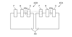
- the first power card 40A and the second power card 40B may be arranged side by side in the thickness direction with the front and back facing the same direction so that the P terminal of the first power card 40A (one semiconductor module) faces the O terminal of the second power card 40B (another semiconductor module).
- the first power card 40A and the second power card 40B are arranged with the ends 49a on which the terminals are arranged facing the same direction, with partial overlap (adjacent) with the front and back facing the same direction.
- the P terminal of the first power card 40A faces the O terminal of the second power card 40B (another semiconductor module), making it easier to connect the P terminal of the first power card 40A and the O terminal of the second power card 40B. Furthermore, the direction in which current flows through the P terminal of the first power card 40A (from the P terminal to the inside of the first power card 40A) is opposite to the direction in which current flows through the O terminal of the second power card 40B (from the inside of the second power card 40B to the O terminal), reducing the inductance of these terminals and reducing losses.
- the inductance of the N terminal of the first power card 40A and the N terminal of the second power card 40B can be reduced, and the surge current can be suppressed.
- the first power card 40A and the second power card 40B may be arranged in the same direction on the front and back, with the P terminal of the first power card 40A (one semiconductor module) and the O terminal of the second power card 40B (another semiconductor module) facing side by side in the arrangement direction of the P terminal, N terminal, and O terminal.
- the first power card 40A and the second power card 40B are arranged adjacent to each other in the same direction on the front and back, with the ends 49a on which the terminals are arranged facing the same direction.
- the P terminal of the first power card 40A one semiconductor module
- the O terminal of the second power card 40B another semiconductor module
- the direction in which current flows through the P terminal of the first power card 40A is opposite to the direction in which current flows through the O terminal of the second power card 40B (from the inside of the second power card 40B to the O terminal), reducing the inductance of these terminals and reducing losses.
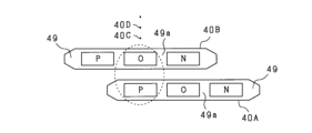
- a P terminal, an O terminal, and an N terminal may be arranged in this order at an end 49a (end in a specific direction) along one long side of the molded resin 49 (power card 40).
- the P terminal and the N terminal are respectively arranged at both ends (near both ends) in the longitudinal direction of the molded resin 49.
- the O terminal is arranged in the center (near the center) of the molded resin 49 in the longitudinal direction.
- the first power card 40A and the second power card 40B may be arranged side by side in the thickness direction with the front and back facing the same direction so that the P terminal of the first power card 40A (one semiconductor module) faces the O terminal of the second power card 40B (another semiconductor module).
- the first power card 40A and the second power card 40B are arranged with the ends 49a on which the terminals are arranged facing the same direction, with partial overlap (adjacent) with the front and back facing the same direction.
- the P terminal of the first power card 40A faces the O terminal of the second power card 40B (another semiconductor module), making it easier to connect the P terminal of the first power card 40A and the O terminal of the second power card 40B. Furthermore, the direction in which current flows through the P terminal of the first power card 40A (from the P terminal to the inside of the first power card 40A) is opposite to the direction in which current flows through the O terminal of the second power card 40B (from the inside of the second power card 40B to the O terminal), reducing the inductance of these terminals and reducing losses.
- first power card 40A and the second power card 40B are arranged side by side in the thickness direction with the front and back facing inversely so that the P terminal of the first power card 40A (one semiconductor module) faces the O terminal of the second power card 40B (another semiconductor module).
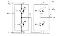
- a circuit equivalent to one phase circuit 170 constituted by the series connection circuit 162 and the AC switch circuit 165 in Fig. 23 is constituted by the output potential switching circuit 50 shown in Fig. 13. Note that the same parts as those in the first embodiment are denoted by the same reference numerals and description thereof will be omitted.
- the output potential switching circuit 50 includes a first power card 40A and a second power card 40B as power cards 40.
- the output potential switching circuit 50 includes only the first diode 42, the first switching element 41, the second diode 44, and the second switching element 43, i.e., only the elements included in each power card 40A, 40B, and does not include any other elements.
- the N terminal of the first power card 40A (first semiconductor module, one semiconductor module) is connected to the O terminal of the second power card 40B (second semiconductor module, another semiconductor module).
- an N terminal, a P terminal, and an O terminal are arranged in this order at an end 49a (end in a specific direction) along one long side of the molded resin 49 (power card 40).
- the N terminal and the O terminal are respectively arranged at both ends (near both ends) in the longitudinal direction of the molded resin 49.
- the P terminal is arranged in the center (near the center) of the molded resin 49 in the longitudinal direction.
- the first power card 40A and the second power card 40B are arranged in the thickness direction with the front and back facing each other so that the N terminal of the first power card 40A faces the O terminal of the second power card 40B.
- the first power card 40A and the second power card 40B are arranged adjacent to each other with the front and back facing each other, with the ends 49a on which the terminals are arranged facing the same direction.
- the outer edge of the first power card 40A and the outer edge of the second power card 40B are aligned.
- the N terminal of the first power card 40A and the O terminal of the second power card 40B are connected.
- the P terminal of the first power card 40A faces the P terminal of the second power card 40B
- the O terminal of the first power card 40A faces the N terminal of the second power card 40B.
- a positive potential Vp is input to the P terminal of the first power card 40A
- a neutral point potential Vm is input to the P terminal of the second power card 40B
- a negative potential Vn is input to the N terminal of the second power card 40B.
- the output potential switching circuit 50 also inputs three levels of potential, and by operating the switching elements 41, 43 of the first and second power cards 40A, 40B, the output potential Vo to one phase coil of the rotating electric machine 12 is switched to one of the three levels of potential.
- the P terminal of the first power card 40A and the P terminal of the second power card 40B face each other. This reduces the inductance of the P terminal of the first power card 40A and the P terminal of the second power card 40B, thereby suppressing surge currents.
- FIG. 18 is a circuit diagram showing an output potential switching circuit 50A applied to a five-level inverter.
- the output potential switching circuit 50A includes a first power card 40A, a second power card 40B, a third power card 40C, and a fourth power card 40D as power cards 40.
- the output potential switching circuit 50A includes only the first diode 42, the first switching element 41, the second diode 44, and the second switching element 43, i.e., only the elements included in each of the power cards 40A to 40D, and does not include any other elements.
- the output potential switching circuit 50A is applied to a five-level (multi-level) inverter, inputs five levels of potential, and switches the output potential Vo to one phase coil of the rotating electric machine 12 to one of the five levels of potential.
- the N terminal of the first power card 40A one semiconductor module
- the N terminal of the second power card 40B one semiconductor module
- the N terminal of the third power card 40C one other semiconductor module
- the N terminal of the third power card 40C (one semiconductor module) is connected to the O terminal of the fourth power card 40D (one other semiconductor module). That is, the N terminal of one power card 40 (one semiconductor module) is connected to the O terminal of the other power card 40.
- the second power card 40B and the third power card 40C are arranged in opposite directions, overlapping in the thickness direction, so that the N terminal of the second power card 40B (one semiconductor module) faces the O terminal of the third power card 40C (another semiconductor module). That is, the third power card 40C is arranged in the same front and back direction as the first power card 40A, overlapping in the thickness direction on the second power card 40B. Furthermore, the third power card 40C and the fourth power card 40D are arranged in opposite directions, overlapping in the thickness direction, so that the N terminal of the third power card 40C (one semiconductor module) faces the O terminal of the fourth power card 40D (another semiconductor module). That is, the fourth power card 40D is arranged in the same front and back direction as the second power card 40B, overlapping in the thickness direction on the third power card 40C.
- a positive potential Vp is input to the P terminal of the first power card 40A
- a first neutral point potential Vm1 is input to the P terminal of the second power card 40B
- a second neutral point potential Vm2 is input to the P terminal of the third power card 40C
- a third neutral point potential Vm3 is input to the P terminal of the fourth power card 40D
- a negative potential Vn is input to the P terminal of the fourth power card 40D (Vp>Vm1>Vm2>Vm3>Vn).
- the O terminal of the first power card 40A to whose P terminal a positive potential Vp (the highest potential) of the multi-level potentials is input, is connected to one phase coil of the rotating electric machine 12, and a potential of the multi-level potentials lower than the potential input to the P terminal of one power card 40 (one semiconductor module) is input to the P terminal of another power card 40 (one other semiconductor module).
- the circuit for one phase composed of the series connection circuit 160 and AC switch circuit 163 for the U phase in FIG. 23 can also be configured in a similar manner using the output potential switching circuit 50.
- the circuit for one phase composed of the series connection circuit 161 and AC switch circuit 164 for the V phase in FIG. 23 can also be configured in a similar manner using the output potential switching circuit 50.
- the positional relationship (arrangement) between the output potential switching circuit 50 for the U phase, the output potential switching circuit 50 for the V phase, and the output potential switching circuit 50 for the W phase is arbitrary.
- the N terminal of the first power card 40A (one power card 40) is connected to the O terminal of the second power card 40B (the other power card 40). Therefore, by inputting a positive potential Vp to the P terminal of the first power card 40A, inputting a neutral point potential Vm to the P terminal of the second power card 40B, and inputting a negative potential Vn to the N terminal of the second power card 40B, and operating the switching elements 41, 43 of the first and second power cards 40A, 40B, the output potential Vo output from the O terminal of the first power card 40A can be switched to any one of the positive potential Vp, the neutral point potential Vm, and the negative potential Vn. Therefore, an output potential switching circuit 50 applicable to a three-level inverter can be configured using a general-purpose power card 40.
- the N terminal of the first power card 40A (one power card 40) faces the O terminal of the second power card 40B (another power card 40)
- the direction of current flowing through the N terminal of the first power card 40A is opposite to the direction of current flowing through the O terminal of the second power card 40B, the inductance of these terminals can be reduced, thereby reducing losses.
- the first power card 40A and the second power card 40B are arranged in opposite directions, stacked in the thickness direction, the arrangement space for multiple power cards 40 can be reduced.
- the output potential switching circuit 50 includes only the first diode 42, the first switching element 41, the second diode 44, and the second switching element 43, and does not include any other elements. Therefore, the output potential switching circuit 50 can be configured without requiring any elements other than those included in the power card 40.
- the second embodiment can also be modified as follows.
- the same parts as those in the second embodiment are given the same reference numerals and will not be described.
- the first power card 40A and the second power card 40B may be arranged side by side in the thickness direction with the front and back facing the same direction so that the N terminal of the first power card 40A (one semiconductor module) faces the O terminal of the second power card 40B (another semiconductor module).
- the first power card 40A and the second power card 40B are arranged with the ends 49a on which the terminals are arranged facing the same direction, with partial overlap (adjacent) with the front and back facing the same direction.
- the first power card 40A and the second power card 40B may be arranged in the same direction on the front and back, with the N terminal of the first power card 40A (one semiconductor module) and the O terminal of the second power card 40B (another semiconductor module) adjacent to each other, with the front and back facing in the same direction.
- the first power card 40A and the second power card 40B are arranged adjacent to each other with the front and back facing in the same direction, with the ends 49a on which the terminals are arranged facing in the same direction.
- a P terminal, an O terminal, and an N terminal may be arranged in this order at an end 49a (end in a specific direction) along one long side of the molded resin 49 (power card 40).
- the P terminal and the N terminal are respectively arranged at both ends (near both ends) in the longitudinal direction of the molded resin 49.
- the O terminal is arranged in the center (near the center) of the molded resin 49 in the longitudinal direction.
- the first power card 40A and the second power card 40B may be arranged side by side in the thickness direction with the front and back facing the same direction so that the N terminal of the first power card 40A (one semiconductor module) faces the O terminal of the second power card 40B (another semiconductor module).
- the first power card 40A and the second power card 40B are arranged so that the ends 49a on which the terminals are arranged face in the same direction and partially overlap (are adjacent to each other) with the front and back facing the same direction. With this configuration, it is possible to achieve the same effect as in FIG. 12.
- first power card 40A and the second power card 40B are arranged side by side in the thickness direction with the front and back facing the opposite direction so that the N terminal of the first power card 40A (one semiconductor module) faces the O terminal of the second power card 40B (another semiconductor module).
- a power card 60 shown in FIG. 22 can be used.
- the power card 60 includes a first switching element 41, a first diode 42, a second switching element 43, and a second diode 44, but does not include a P terminal, a wiring connecting the first switching element 41 and the second switching element 43, an O terminal, or an N terminal.
- the power card 40 may be configured by providing a P terminal, a wiring connecting the first switching element 41 and the second switching element 43, an O terminal, and an N terminal outside the power card 60.
- the power card 40 may be configured by providing a member that the power card does not include outside.
Landscapes
- Engineering & Computer Science (AREA)
- Power Engineering (AREA)
- Inverter Devices (AREA)
Abstract
出力電位切替回路(30)は、マルチレベルインバータに適用され、マルチレベルの電位を入力し、出力電位をマルチレベルの電位のいずれか1つに切り替える。出力電位切替回路は、第1ダイオード(42)が逆並列接続された第1スイッチング(41)素子と、第2ダイオード(44)が逆並列接続された第2スイッチング素子(43)と、第1スイッチング素子の正極端子が接続されたP端子と、第1スイッチング素子の負極端子及び第2スイッチング素子の正極端子が接続されたO端子と、第2スイッチング素子の負極端子が接続されたN端子とを備える半導体モジュール(40A、40B)、を複数備え、1つの半導体モジュール(40A)のP端子と、他の1つの半導体モジュール(40B)のO端子とが接続されている。
Description
本出願は、2022年9月28日に出願された日本出願番号2022-155005号に基づくもので、ここにその記載内容を援用する。
本開示は、マルチレベルインバータに適用される出力電位切替回路に関する。
従来、3レベルインバータに適用される半導体モジュールにおいて、直流電源のPN間に接続されるIGBTの直列接続回路と、この直列接続回路の直列接続点と直流電源の中性点との間に接続する交流スイッチ素子とを、1つのパッケージに内蔵したものがある(特許文献1参照)。こうした構成によれば、配線インダクタンスの低減と装置の低価格化を実現することができるとしている。
ところで、特許文献1に記載の半導体モジュール(出力電位切替回路)を生産するためには、専用の半導体モジュールを開発し、新たな生産ラインを立ち上げる必要がある。このため、半導体モジュールを生産するための総コストが高くなるおそれがある。
本開示は、上記課題を解決するためになされたものであり、その主たる目的は、汎用半導体モジュールを用いてマルチレベルインバータに適用される出力電位切替回路を構成することにある。
上記課題を解決するための第1の手段は、
マルチレベルインバータに適用され、マルチレベルの電位を入力し、出力電位を前記マルチレベルの電位のいずれか1つに切り替える出力電位切替回路であって、
第1ダイオードが逆並列接続された第1スイッチング素子と、第2ダイオードが逆並列接続された第2スイッチング素子と、前記第1スイッチング素子の正極端子が接続されたP端子と、前記第1スイッチング素子の負極端子及び前記第2スイッチング素子の正極端子が接続されたO端子と、前記第2スイッチング素子の負極端子が接続されたN端子とを備える半導体モジュール、を複数備え、
1つの前記半導体モジュールの前記P端子と、他の1つの前記半導体モジュールの前記O端子とがそれぞれ接続されている。
マルチレベルインバータに適用され、マルチレベルの電位を入力し、出力電位を前記マルチレベルの電位のいずれか1つに切り替える出力電位切替回路であって、
第1ダイオードが逆並列接続された第1スイッチング素子と、第2ダイオードが逆並列接続された第2スイッチング素子と、前記第1スイッチング素子の正極端子が接続されたP端子と、前記第1スイッチング素子の負極端子及び前記第2スイッチング素子の正極端子が接続されたO端子と、前記第2スイッチング素子の負極端子が接続されたN端子とを備える半導体モジュール、を複数備え、
1つの前記半導体モジュールの前記P端子と、他の1つの前記半導体モジュールの前記O端子とがそれぞれ接続されている。
上記構成によれば、出力電位切替回路は、マルチレベルインバータに適用され、マルチレベルの電位を入力し、出力電位を前記マルチレベルの電位のいずれか1つに切り替える。
ここで、出力電位切替回路は、第1ダイオードが逆並列接続された第1スイッチング素子と、第2ダイオードが逆並列接続された第2スイッチング素子と、前記第1スイッチング素子の正極端子が接続されたP端子と、前記第1スイッチング素子の負極端子及び前記第2スイッチング素子の正極端子が接続されたO端子と、前記第2スイッチング素子の負極端子が接続されたN端子とを備える半導体モジュール(以下、「汎用半導体モジュール」という)、を複数備えている。汎用半導体モジュールは、3相の2レベルインバータ等に汎用され、1相分の回路を構成する半導体モジュールである。
そして、1つの前記半導体モジュール(以下、「第1半導体モジュール」という)の前記P端子と、他の1つの前記半導体モジュール(以下、「第2半導体モジュール」という)の前記O端子とがそれぞれ接続されている。このため、例えば出力電位切替回路が第1半導体モジュール及び第2半導体モジュールのみで構成されている場合、第2半導体モジュールのP端子に正極電位を入力し、第2半導体モジュールのN端子に中性点電位を入力し、第1半導体モジュールのN端子に負極電位を入力し、第1,第2半導体モジュールのスイッチング素子を操作することにより、第1半導体モジュールのO端子から出力される出力電位を正極電位、中性点電位、及び負極電位のいずれか1つに切り替えることができる。したがって、汎用半導体モジュールを用いてマルチレベルインバータに適用される出力電位切替回路を構成することができる。
なお、第2半導体モジュール(1つの前記半導体モジュール)のP端子に他の1つの前記半導体モジュール(以下、「第3半導体モジュール」という)の前記O端子が接続されている場合は、第3半導体モジュールのP端子に正極電位を入力し、第3半導体モジュールのN端子に第1中間電位を入力し、第2半導体モジュールのN端子に第2中間電位を入力し、第1半導体モジュールのN端子に負極電位を入力することにより、4レベルインバータに適用される出力電位切替回路を構成することができる。同様にして、さらに汎用半導体モジュールを追加することにより、5レベル以上のインバータに適用される出力電位切替回路も構成することができる。
第2の手段では、前記半導体モジュールは、板状に形成され、前記半導体モジュールの所定方向の端部に前記P端子、前記N端子、及び前記O端子がこの順で並んで配置され、前記1つの前記半導体モジュールの前記P端子が、前記他の1つの前記半導体モジュールの前記O端子に対向するように、前記1つの前記半導体モジュールと前記他の1つの前記半導体モジュールとが表裏逆向きで板厚方向に重ねて配置されている。
上記構成によれば、前記1つの前記半導体モジュールの前記P端子が、前記他の1つの前記半導体モジュールの前記O端子に対向しているため、前記1つの前記半導体モジュールの前記P端子と、前記他の1つの前記半導体モジュールの前記O端子とを接続しやすくなる。さらに、前記1つの前記半導体モジュールのP端子に電流が流れる方向と、前記他の1つの前記半導体モジュールのO端子に電流が流れる方向とが逆になるため、これらの端子のインダクタンスを低減して損失を低減することができる。しかも、前記1つの前記半導体モジュールと前記他の1つの前記半導体モジュールとが表裏逆向きで板厚方向に重ねて配置されているため、複数の半導体モジュールの配置スペースを小さくすることができる。
第3の手段では、前記半導体モジュールは、板状に形成され、前記半導体モジュールの所定方向の端部に前記P端子、前記N端子、及び前記O端子がこの順で並んで配置され、前記1つの前記半導体モジュールの前記P端子が、前記他の1つの前記半導体モジュールの前記O端子に対向するように、前記1つの前記半導体モジュールと前記他の1つの前記半導体モジュールとが表裏同じ向きで板厚方向に並べて配置されている。
上記構成によれば、前記1つの前記半導体モジュールの前記P端子が、前記他の1つの前記半導体モジュールの前記O端子に対向しているため、前記1つの前記半導体モジュールの前記P端子と、前記他の1つの前記半導体モジュールの前記O端子とを接続しやすくなる。さらに、前記1つの前記半導体モジュールのP端子に電流が流れる方向と、前記他の1つの前記半導体モジュールのO端子に電流が流れる方向とが逆になるため、これらの端子のインダクタンスを低減して損失を低減することができる。
第4の手段では、前記半導体モジュールは、板状に形成され、前記半導体モジュールの所定方向の端部に前記P端子、前記N端子、及び前記O端子がこの順で並んで配置され、前記1つの前記半導体モジュールの前記P端子と、前記他の1つの前記半導体モジュールの前記O端子とが隣り合うように、前記1つの前記半導体モジュールと前記他の1つの前記半導体モジュールとが表裏同じ向きで、前記P端子、前記N端子、及び前記O端子の並び方向に並べて配置されている。
上記構成によれば、前記1つの前記半導体モジュールの前記P端子と、前記他の1つの前記半導体モジュールの前記O端子とが隣り合っているため、前記1つの前記半導体モジュールの前記P端子と、前記他の1つの前記半導体モジュールの前記O端子とを接続しやすくなる。さらに、前記1つの前記半導体モジュールのP端子に電流が流れる方向と、前記他の1つの前記半導体モジュールのO端子に電流が流れる方向とが逆になるため、これらの端子のインダクタンスを低減して損失を低減することができる。
第5の手段では、前記半導体モジュールは、板状に形成され、前記半導体モジュールの所定方向の端部に前記P端子、前記O端子、及び前記N端子がこの順で並んで配置され、前記1つの前記半導体モジュールの前記P端子が、前記他の1つの前記半導体モジュールの前記O端子に対向するように、前記1つの前記半導体モジュールと前記他の1つの前記半導体モジュールとが表裏同じ向き又は表裏逆向きで板厚方向に並べて配置されている。
上記構成によれば、前記1つの前記半導体モジュールの前記P端子が、前記他の1つの前記半導体モジュールの前記O端子に対向しているため、前記1つの前記半導体モジュールの前記P端子と、前記他の1つの前記半導体モジュールの前記O端子とを接続しやすくなる。さらに、前記1つの前記半導体モジュールのP端子に電流が流れる方向と、前記他の1つの前記半導体モジュールのO端子に電流が流れる方向とが逆になるため、これらの端子のインダクタンスを低減して損失を低減することができる。
具体的には、第6の手段のように、前記N端子に前記マルチレベルの電位のうち最も低い電位が入力される前記半導体モジュールの前記O端子が回転電機の1つの相コイルに接続され、前記マルチレベルの電位のうち前記1つの前記半導体モジュールの前記N端子に入力される電位よりも高い電位が、前記他の1つの前記半導体モジュールの前記N端子にそれぞれ入力される、といった構成を採用することができる。こうした構成によれば、回転電機の1つの相コイルに1つの出力電位切替回路を対応させて、回転電機の1つの相コイルに出力される電位をマルチレベルの電位に切り替えることができる。
第7の手段は、
マルチレベルインバータに適用され、マルチレベルの電位を入力し、出力電位を前記マルチレベルの電位のいずれか1つに切り替える出力電位切替回路であって、
第1ダイオードが逆並列接続された第1スイッチング素子と、第2ダイオードが逆並列接続された第2スイッチング素子と、前記第1スイッチング素子の正極端子が接続されたP端子と、前記第1スイッチング素子の負極端子及び前記第2スイッチング素子の正極端子が接続されたO端子と、前記第2スイッチング素子の負極端子が接続されたN端子とを備える半導体モジュール、を複数備え、
1つの前記半導体モジュールの前記N端子と、他の1つの前記半導体モジュールの前記O端子とがそれぞれ接続されている。
マルチレベルインバータに適用され、マルチレベルの電位を入力し、出力電位を前記マルチレベルの電位のいずれか1つに切り替える出力電位切替回路であって、
第1ダイオードが逆並列接続された第1スイッチング素子と、第2ダイオードが逆並列接続された第2スイッチング素子と、前記第1スイッチング素子の正極端子が接続されたP端子と、前記第1スイッチング素子の負極端子及び前記第2スイッチング素子の正極端子が接続されたO端子と、前記第2スイッチング素子の負極端子が接続されたN端子とを備える半導体モジュール、を複数備え、
1つの前記半導体モジュールの前記N端子と、他の1つの前記半導体モジュールの前記O端子とがそれぞれ接続されている。
上記構成によれば、第1の手段と同様に、出力電位切替回路は汎用半導体モジュールを複数備えている。そして、1つの前記半導体モジュール(以下、「第1半導体モジュール」という)の前記N端子と、他の1つの前記半導体モジュール(以下、「第2半導体モジュール」という)の前記O端子とがそれぞれ接続されている。このため、例えば出力電位切替回路が第1半導体モジュール及び第2半導体モジュールのみで構成されている場合、第1半導体モジュールのP端子に正極電位を入力し、第2半導体モジュールのP端子に中性点電位を入力し、第2半導体モジュールのN端子に負極電位を入力し、第1,第2半導体モジュールのスイッチング素子を操作することにより、第1半導体モジュールのO端子から出力される出力電位を正極電位、中性点電位、及び負極電位のいずれか1つの電位に切り替えることができる。したがって、汎用半導体モジュールを用いてマルチレベルインバータに適用される出力電位切替回路を構成することができる。
なお、第2半導体モジュール(1つの前記半導体モジュール)のN端子に他の1つの前記半導体モジュール(以下、「第3半導体モジュール」という)の前記O端子を接続されている場合は、第1半導体モジュールのP端子に正極電位を入力し、第2半導体モジュールのP端子に第1中間電位を入力し、第3半導体モジュールのP端子に第2中間電位を入力し、第3半導体モジュールのN端子に負極電位を入力することにより、4レベルインバータに適用される出力電位切替回路を構成することができる。同様にして、さらに汎用半導体モジュールを追加することにより、5レベル以上のインバータに適用される出力電位切替回路も構成することができる。
第8の手段では、前記半導体モジュールは、板状に形成され、前記半導体モジュールの所定方向の端部に前記N端子、前記P端子、及び前記O端子がこの順で並んで配置され、前記1つの前記半導体モジュールの前記N端子が、前記他の1つの前記半導体モジュールの前記O端子に対向するように、前記1つの前記半導体モジュールと前記他の1つの前記半導体モジュールとが表裏逆向きで板厚方向に重ねて配置されている。
上記構成によれば、前記1つの前記半導体モジュールの前記N端子が、前記他の1つの前記半導体モジュールの前記O端子に対向しているため、前記1つの前記半導体モジュールの前記N端子と、前記他の1つの前記半導体モジュールの前記O端子とを接続しやすくなる。さらに、前記1つの前記半導体モジュールのN端子に電流が流れる方向と、前記他の1つの前記半導体モジュールのO端子に電流が流れる方向とが逆になるため、これらの端子のインダクタンスを低減して損失を低減することができる。しかも、前記1つの前記半導体モジュールと前記他の1つの前記半導体モジュールとが表裏逆向きで板厚方向に重ねて配置されているため、複数の半導体モジュールの配置スペースを小さくすることができる。
第9の手段では、前記半導体モジュールは、板状に形成され、前記半導体モジュールの所定方向の端部に前記N端子、前記P端子、及び前記O端子がこの順で並んで配置され、前記1つの前記半導体モジュールの前記N端子が、前記他の1つの前記半導体モジュールの前記O端子に対向するように、前記1つの前記半導体モジュールと前記他の1つの前記半導体モジュールとが表裏同じ向きで板厚方向に並べて配置されている。
上記構成によれば、前記1つの前記半導体モジュールの前記N端子が、前記他の1つの前記半導体モジュールの前記O端子に対向しているため、前記1つの前記半導体モジュールの前記N端子と、前記他の1つの前記半導体モジュールの前記O端子とを接続しやすくなる。さらに、前記1つの前記半導体モジュールのN端子に電流が流れる方向と、前記他の1つの前記半導体モジュールのO端子に電流が流れる方向とが逆になるため、これらの端子のインダクタンスを低減して損失を低減することができる。
第10の手段では、前記半導体モジュールは、板状に形成され、前記半導体モジュールの所定方向の端部に前記N端子、前記P端子、及び前記O端子がこの順で並んで配置され、前記1つの前記半導体モジュールの前記N端子と、前記他の1つの前記半導体モジュールの前記O端子とが隣り合うように、前記1つの前記半導体モジュールと前記他の1つの前記半導体モジュールとが表裏同じ向きで、前記N端子、前記P端子、及び前記O端子の並び方向に並べて配置されている。
上記構成によれば、前記1つの前記半導体モジュールの前記N端子と、前記他の1つの前記半導体モジュールの前記O端子とが隣り合っているため、前記1つの前記半導体モジュールの前記N端子と、前記他の1つの前記半導体モジュールの前記O端子とを接続しやすくなる。さらに、前記1つの前記半導体モジュールのN端子に電流が流れる方向と、前記他の1つの前記半導体モジュールのO端子に電流が流れる方向とが逆になるため、これらの端子のインダクタンスを低減して損失を低減することができる。
第11の手段では、前記半導体モジュールは、板状に形成され、前記半導体モジュールの所定方向の端部に前記P端子、前記O端子、及び前記N端子がこの順で並んで配置され、前記1つの前記半導体モジュールの前記N端子が、前記他の1つの前記半導体モジュールの前記O端子に対向するように、前記1つの前記半導体モジュールと前記他の1つの前記半導体モジュールとが表裏同じ向き又は表裏逆向きで板厚方向に並べて配置されている。
上記構成によれば、前記1つの前記半導体モジュールの前記N端子が、前記他の1つの前記半導体モジュールの前記O端子に対向しているため、前記1つの前記半導体モジュールの前記N端子と、前記他の1つの前記半導体モジュールの前記O端子とを接続しやすくなる。さらに、前記1つの前記半導体モジュールのN端子に電流が流れる方向と、前記他の1つの前記半導体モジュールのO端子に電流が流れる方向とが逆になるため、これらの端子のインダクタンスを低減して損失を低減することができる。
具体的には、第12の手段のように、前記P端子に前記マルチレベルの電位のうち最も高い電位が入力される前記半導体モジュールの前記O端子が回転電機の1つの相コイルに接続され、前記マルチレベルの電位のうち前記1つの前記半導体モジュールの前記P端子に入力される電位よりも低い電位が、前記他の1つの前記半導体モジュールの前記P端子にそれぞれ入力される、といった構成を採用することができる。こうした構成によれば、回転電機の1つの相コイルに1つの出力電位切替回路を対応させて、回転電機の1つの相コイルに出力される電位をマルチレベルの電位に切り替えることができる。
第13の手段は、
マルチレベルインバータに適用され、マルチレベルの電位を入力し、出力電位を前記マルチレベルの電位のいずれか1つに切り替える出力電位切替回路であって、
第1ダイオードが逆並列接続された第1スイッチング素子と、第2ダイオードが逆並列接続された第2スイッチング素子と、前記第1スイッチング素子の正極端子が接続されたP端子と、前記第1スイッチング素子の負極端子及び前記第2スイッチング素子の正極端子が接続されたO端子と、前記第2スイッチング素子の負極端子が接続されたN端子とを備える半導体モジュール、を複数備え、
前記第1ダイオード、前記第1スイッチング素子、前記第2ダイオード、及び前記第2スイッチング素子のみを素子として備え、他の素子を備えていない。
マルチレベルインバータに適用され、マルチレベルの電位を入力し、出力電位を前記マルチレベルの電位のいずれか1つに切り替える出力電位切替回路であって、
第1ダイオードが逆並列接続された第1スイッチング素子と、第2ダイオードが逆並列接続された第2スイッチング素子と、前記第1スイッチング素子の正極端子が接続されたP端子と、前記第1スイッチング素子の負極端子及び前記第2スイッチング素子の正極端子が接続されたO端子と、前記第2スイッチング素子の負極端子が接続されたN端子とを備える半導体モジュール、を複数備え、
前記第1ダイオード、前記第1スイッチング素子、前記第2ダイオード、及び前記第2スイッチング素子のみを素子として備え、他の素子を備えていない。
上記構成によれば、第1の手段と同様に、出力電位切替回路は汎用半導体モジュールを複数備えている。例えば、1つの前記半導体モジュール(以下、「第1半導体モジュール」という)の前記P端子と、他の1つの前記半導体モジュール(以下、「第2半導体モジュール」という)の前記O端子とをそれぞれ接続することにより、第1の手段と同様の作用効果を奏することができる。また、第1半導体モジュールの前記N端子と、第2半導体モジューの前記O端子とをそれぞれ接続することにより、第7の手段と同様の作用効果を奏することができる。さらに、出力電位切替回路は、前記第1ダイオード、前記第1スイッチング素子、前記第2ダイオード、及び前記第2スイッチング素子のみを素子として備え、他の素子を備えていない。したがって、汎用半導体モジュールに含まれる素子以外の素子を必要とせずに出力電位切替回路を構成することができる。
本開示についての上記目的およびその他の目的、特徴や利点は、添付の図面を参照しながら下記の詳細な記述により、より明確になる。その図面は、
図1は、パワーカードの回路構成を示す模式図であり、
図2は、パワーカードの正面を示す模式図であり、
図3は、パワーカードの上面を示す模式図であり、
図4は、第1実施形態の3レベルインバータに適用される出力電位切替回路を示す回路図であり、
図5は、パワーカードの配置を示す平面図であり、
図6は、第1実施形態の出力電位切替回路及びその周辺構成を示す回路図であり、
図7は、スイッチング素子切替時の電流の流れを示す回路図であり、
図8は、5レベルインバータに適用される出力電位切替回路を示す回路図であり、
図9は、パワーカードの配置の変更例を示す平面図であり、
図10は、パワーカードの配置の他の変更例を示す平面図であり、
図11は、パワーカードの変更例の正面を示す模式図であり、
図12は、パワーカードの配置の他の変更例を示す平面図であり、
図13は、第2実施形態の3レベルインバータに適用される出力電位切替回路を示す回路図であり、
図14は、パワーカードの正面を示す模式図であり、
図15は、パワーカードの配置を示す平面図であり、
図16は、第2実施形態の出力電位切替回路及びその周辺構成を示す回路図であり、
図17は、スイッチング素子切替時の電流の流れを示す回路図であり、
図18は、5レベルインバータに適用される出力電位切替回路を示す回路図であり、
図19は、パワーカードの配置の変更例を示す平面図であり、
図20は、パワーカードの配置の他の変更例を示す平面図であり、
図21は、パワーカードの配置の他の変更例を示す平面図であり、
図22は、パワーカードの回路構成の変更例を示す模式図であり、
図23は、従来の3レベルインバータ及びその周辺構成を示す回路図である。
(第1実施形態)
以下、車両に搭載される直流電源と回転電機との間で電力を変換する3レベルインバータ(マルチレベルインバータ)に適用される出力電位切替回路に具現化した第1実施形態について、図面を参照しつつ説明する。車両は、電気自動車やハイブリッド自動車等である。回転電機は、モータ、発電機、MG(Motor Generator)等である。
以下、車両に搭載される直流電源と回転電機との間で電力を変換する3レベルインバータ(マルチレベルインバータ)に適用される出力電位切替回路に具現化した第1実施形態について、図面を参照しつつ説明する。車両は、電気自動車やハイブリッド自動車等である。回転電機は、モータ、発電機、MG(Motor Generator)等である。
図23は、従来の3レベルインバータ及びその周辺構成を示す回路図である。電池11の電圧Vhが、コンデンサC1,C2により電圧Vh/2ずつに分圧されてインバータ120へ供給される。これにより、コンデンサC1,C2は3レベルの電位を出力する直流電源13として機能する。ここでは、コンデンサC1の正極側の電位を正極電位Vp、コンデンサC2の負極側の電位を負極電位Vn、コンデンサC1の負極側とコンデンサC2の正極側との接続点(中性点M)の電位を中性点電位Vmとしている。
正極電位Vpと負極電位Vnとの間には、ダイオードを逆並列接続したMOSFETの直列接続回路が3相分接続されている。すなわち、U相用の直列接続回路160はダイオード112を逆並列接続したMOSFET111からなる上アームとダイオード114を逆並列接続したMOSFET113からなる下アームとの直列接続回路で構成されている。V相用の直列接続回路161はダイオード122を逆並列接続したMOSFET121からなる上アームとダイオード124を逆並列接続したMOSFET123からなる下アームとの直列接続回路で構成されている。W相用の直列接続回路162はダイオード132を逆並列接続したMOSFET131からなる上アームとダイオード134を逆並列接続したMOSFET133からなる下アームとの直列接続回路で構成されている。
各相の直列接続回路の上アームと下アームの直列接続点と中性点電位Vmとの間には、ダイオードを逆並列接続したMOSFETを逆直列接続した交流スイッチが接続されている。すなわち、U相用の直列接続回路160の直列接続点と直流電源13の中性点Mとの間には、ダイオード182を逆並列接続したMOSFET181のソースとダイオード184を逆並列接続したMOSFET183のソースとが接続された構成の交流スイッチ回路163が接続されている。V相用の直列接続回路161の直列接続点と直流電源13の中性点Mとの間には、ダイオード186を逆並列接続したMOSFET185のソースとダイオード188を逆並列接続したMOSFET187のソースとが接続された構成の交流スイッチ回路164が接続されている。W相用の直列接続回路162の直列接続点と直流電源13の中性点Mとの間には、ダイオード190を逆並列接続したMOSFET189のソースとダイオード192を逆並列接続したMOSFET191のソースとが接続された構成の交流スイッチ回路165が接続されている。また、各直列接続回路160,161,162の直列接続点は交流出力となり、回転電機12の各相コイル12u,12v,12wに接続されている。
上記構成によれば、各直列接続回路160、161、162の直列接続点は、正極電位Vp、負極電位Vn、及び中性点電位Vmを出力することが可能となるため、3レベルのインバータ出力となる。
本実施形態では、例えばW相用の直列接続回路162及び交流スイッチ回路165により構成される1相分の回路170を、2枚のパワーカードにより構成する。パワーカード(汎用半導体モジュール、半導体モジュール)は、3相の2レベルインバータ等に汎用され、1相分の回路を構成する半導体モジュールである。
図1は、パワーカード40の回路構成を示す模式図である。パワーカード40(2in1モジュール)は、第1スイッチング素子41、第1ダイオード42、第2スイッチング素子43、第2ダイオード44、P端子、O端子、N端子、及びモールド樹脂49等を備えている。第1スイッチング素子41は、例えばIGBT(Insulated Gate Bipolar Transistor)、MOSFET(Metal-Oxide-Semiconductor Field-Effect Transistor)等の半導体素子である。ここでは、IGBTを例にして説明する。第1スイッチング素子41には、第1ダイオード42が逆並列接続されている。第2スイッチング素子43には、第2ダイオード44が逆並列接続されている。第1スイッチング素子41のコレクタ(正極端子)には、P端子が接続されている。第1スイッチング素子41のエミッタ(負極端子)には、第2スイッチング素子43のコレクタ(正極端子)が接続されている。第1スイッチング素子41のエミッタ及び第2スイッチング素子43のコレクタは、O端子に接続されている。すなわち、第1スイッチング素子41と第2スイッチング素子43との直列接続点45がO端子に接続されている。第2スイッチング素子43のエミッタ(負極端子)には、N端子が接続されている。そして、第1スイッチング素子41、第1ダイオード42、第2スイッチング素子43、及び第2ダイオード44は、モールド樹脂49(封止樹脂)により封止されている。
図2はパワーカード40の正面を示す模式図であり、図3はパワーカード40の上面を示す模式図である。モールド樹脂49(パワーカード40)は、矩形板状(板状)に形成されている。モールド樹脂49(パワーカード40)の1つの長辺に沿った端部49a(所定方向の端部)に、P端子、N端子、O端子がこの順で並んで配置されている。P端子、N端子、及びO端子は、金属合金(導体)により矩形板状(板状、棒状)に形成されている。P端子、N端子、及びO端子は、モールド樹脂49から外部に露出している。P端子及びO端子は、モールド樹脂49の長手方向の両端部(両端部付近)にそれぞれ配置されている。N端子は、モールド樹脂49の長手方向の中央部(中央部付近)に配置されている。
図4は、出力電位切替回路30を示す回路図である。出力電位切替回路30は、図23の直列接続回路162及び交流スイッチ回路165により構成される1相分の回路170に相当する回路である。出力電位切替回路30は、パワーカード40としての第1パワーカード40A及び第2パワーカード40Bを備えている。出力電位切替回路30は、第1ダイオード42、第1スイッチング素子41、第2ダイオード44、及び第2スイッチング素子43のみ、すなわち各パワーカード40A,40Bに含まれる各素子のみを素子として備え、他の素子を備えていない。第1パワーカード40A(第1半導体モジュール、1つの半導体モジュール)のP端子と、第2パワーカード40B(第2半導体モジュール、他の1つの半導体モジュール)のO端子とが接続されている。
図5に示すように、第1パワーカード40AのP端子が、第2パワーカード40BのO端子に対向するように、第1パワーカード40Aと第2パワーカード40Bとが表裏逆向きで板厚方向に重ねて配置されている。具体的には、第1パワーカード40Aと第2パワーカード40Bとが、各端子の配置された端部49aを同じ方向に向けて、表裏逆向きで隣り合うように配置されている。第1パワーカード40Aの正面視(板面に垂直な方向への投影)において、第1パワーカード40Aの外縁と第2パワーカード40Bの外縁とが一致している。そして、破線の円で示すように、第1パワーカード40AのP端子と第2パワーカード40BのO端子とが接続されている。なお、第1パワーカード40AのN端子と第2パワーカード40BのN端子とが対向し、第1パワーカード40AのO端子と第2パワーカード40BのP端子とが対向している。
図6は、出力電位切替回路30及びその周辺構成を示す回路図である。なお、図23と同一とみなせる部分については、同一の符号を付すことにより説明を省略する。
第2パワーカード40BのP端子に正極電位Vpが入力され、第2パワーカード40BのN端子に中性点電位Vmが入力され、第1パワーカード40AのN端子に負極電位Vnが入力される。そして、出力電位切替回路30は、3レベル(マルチレベル)インバータに適用され、3レベルの電位を入力し、回転電機12の1つの相コイルへの出力電位Voを3レベルの電位のいずれか1つに切り替える。具体的には、第2パワーカード40Bの第1スイッチング素子41及び第1パワーカード40Aの第1スイッチング素子41をONにし、第2パワーカード40Bの第2スイッチング素子43及び第1パワーカード40Aの第2スイッチング素子43をOFFにすることにより、第1パワーカード40AのO端子から出力電位Vpが出力される。第2パワーカード40Bの第2スイッチング素子43及び第1パワーカード40Aの第1スイッチング素子41をONにし、第2パワーカード40Bの第1スイッチング素子41及び第1パワーカード40Aの第2スイッチング素子43をOFFにすることにより、第1パワーカード40AのO端子から中性点電位Vmが出力される。第1パワーカード40Aの第1スイッチング素子41をOFFにし、第1パワーカード40Aの第2スイッチング素子43をONにすることにより、第1パワーカード40AのO端子から負極電位Vnが出力される。
上記において、第2パワーカード40BのO端子から電流が出て、第1パワーカード40AのP端子へ電流が入る。このため、第2パワーカード40BのO端子に電流が流れる方向と、第1パワーカード40AのP端子に電流が流れる方向とが逆になる。そして、第1パワーカード40AのP端子と、第2パワーカード40BのO端子とが対向している。したがって、第2パワーカード40BのO端子と第1パワーカード40AのP端子との間に相互インダクタンスが発生し、第2パワーカード40BのO端子及び第1パワーカード40AのP端子のインダクタンスが低減される。
図7に示すように、第2パワーカード40Bの第1スイッチング素子41をOFF且つ第2スイッチング素子43をON、且つ、第1パワーカード40Aの第1スイッチング素子41をON且つ第2スイッチング素子43をOFFの状態から、第1パワーカード40Aの第1スイッチング素子41をOFF且つ第2スイッチング素子43をONの状態に切り替える際には、矢印で示すサージ電流が流れる。ここで、第2パワーカード40BのO端子及び第1パワーカード40AのP端子のインダクタンスが低減されているため、このサージ電流を抑制することができる。また、第2パワーカード40BのN端子に電流が流れる方向と、第1パワーカード40AのN端子に電流が流れる方向とが逆になる。そして、図5に示すように、第1パワーカード40AのN端子と、第2パワーカード40BのN端子とが対向している。このため、第1パワーカード40AのN端子及び第2パワーカード40BのN端子のインダクタンスを低減することができ、サージ電流を抑制することができる。
図8は、5レベルインバータに適用される出力電位切替回路30Aを示す回路図である。出力電位切替回路30Aは、パワーカード40としての第1パワーカード40A、第2パワーカード40B、第3パワーカード40C、及び第4パワーカード40Dを備えている。出力電位切替回路30Aは、第1ダイオード42、第1スイッチング素子41、第2ダイオード44、及び第2スイッチング素子43のみ、すなわち各パワーカード40A~40Dに含まれる各素子のみを素子として備え、他の素子を備えていない。
出力電位切替回路30Aは、5レベル(マルチレベル)インバータに適用され、5レベルの電位を入力し、回転電機12の1つの相コイルへの出力電位Voを5レベルの電位のいずれか1つに切り替える。この場合、第1パワーカード40A(1つの半導体モジュール)のP端子と、第2パワーカード40B(他の1つの半導体モジュール)のO端子とが接続されている。第2パワーカード40B(1つの半導体モジュール)のP端子と、第3パワーカード40C(他の1つの半導体モジュール)のO端子とが接続されている。第3パワーカード40C(1つの半導体モジュール)のP端子と、第4パワーカード40D(他の1つの半導体モジュール)のO端子とが接続されている。すなわち、1つのパワーカード40(1つの半導体モジュール)のP端子と、他の1つのパワーカード40(他の1つの半導体モジュール)のO端子とがそれぞれ接続されている。
この場合は、図5に点々で示すように、第2パワーカード40B(1つの半導体モジュール)のP端子が、第3パワーカード40C(他の1つの半導体モジュール)のO端子に対向するように、第2パワーカード40Bと第3パワーカード40Cとが表裏逆向きで板厚方向に重ねて配置されている。すなわち、第3パワーカード40Cは、第1パワーカード40Aと表裏同じ向きで、第2パワーカード40Bに板厚方向に重ねて配置されている。さらに、第3パワーカード40C(1つの半導体モジュール)のP端子が、第4パワーカード40D(他の1つの半導体モジュール)のO端子に対向するように、第3パワーカード40Cと第4パワーカード40Dとが表裏逆向きで板厚方向に重ねて配置されている。すなわち、第4パワーカード40Dは、第2パワーカード40Bと表裏同じ向きで、第3パワーカード40Cに板厚方向に重ねて配置されている。
図8に示すように、第4パワーカード40DのP端子に正極電位Vpが入力され、第4パワーカード40DのN端子に第1中性点電位Vm1が入力され、第3パワーカード40CのN端子に第2中性点電位Vm2が入力され、第2パワーカード40BのN端子に第3中性点電位Vm3が入力され、第1パワーカード40AのN端子に負極電位Vnが入力される(Vp>Vm1>Vm2>Vm3>Vn)。すなわち、N端子にマルチレベルの電位のうち負極電位Vn(最も低い電位)が入力される第1パワーカード40AのO端子が回転電機12の1つの相コイルに接続され、マルチレベルの電位のうち1つのパワーカード40(1つの半導体モジュール)のN端子に入力される電位よりも高い電位が、他の1つのパワーカード40(他の1つの半導体モジュール)のN端子に入力される。
また、図23のU相用の直列接続回路160及び交流スイッチ回路163により構成される1相分の回路も、同様にして出力電位切替回路30により構成することができる。図23のV相用の直列接続回路161及び交流スイッチ回路164により構成される1相分の回路も、同様にして出力電位切替回路30により構成することができる。U相分の出力電位切替回路30と、V相分の出力電位切替回路30と、W相分の出力電位切替回路30との位置関係(配置)は任意である。
以上詳述した本実施形態は、以下の利点を有する。
・第1パワーカード40A(1つのパワーカード40)のP端子と、第2パワーカード40B(他の1つのパワーカード40)のO端子とが接続されている。このため、第2パワーカード40BのP端子に正極電位Vpを入力し、第2パワーカード40BのN端子に中性点電位Vmを入力し、第1パワーカード40AのN端子に負極電位Vnを入力し、第1,第2パワーカード40A,40Bのスイッチング素子41,43を操作することにより、第1パワーカード40AのO端子から出力される出力電位Voを正極電位Vp、中性点電位Vm、及び負極電位Vnのいずれか1つに切り替えることができる。したがって、汎用のパワーカード40を用いて3レベルインバータに適用される出力電位切替回路30を構成することができる。
・パワーカード40を追加することにより、5レベルインバータ(4レベル以上のインバータ)に適用される出力電位切替回路30Aも構成することができる。
・第1パワーカード40A(1つのパワーカード40)のP端子が、第2パワーカード40B(他の1つのパワーカード40)のO端子に対向しているため、第1パワーカード40AのP端子と、第2パワーカード40BのO端子とを接続しやすくなる。さらに、第1パワーカード40AのP端子に電流が流れる方向と、第2パワーカード40BのO端子に電流が流れる方向とが逆になるため、これらの端子のインダクタンスを低減して損失を低減することができる。しかも、第1パワーカード40Aと第2パワーカード40Bとが表裏逆向きで板厚方向に重ねて配置されているため、複数のパワーカード40の配置スペースを小さくすることができる。
・第2パワーカード40Bの第1スイッチング素子41をOFF且つ第2スイッチング素子43をON、且つ、第1パワーカード40Aの第1スイッチング素子41をON且つ第2スイッチング素子43をOFFの状態から、第1パワーカード40Aの第1スイッチング素子41をOFF且つ第2スイッチング素子43をONの状態に切り替える際に、第2パワーカード40BのN端子に電流が流れる方向と、第1パワーカード40AのN端子に電流が流れる方向とが逆になる。そして、第1パワーカード40AのN端子と、第2パワーカード40BのN端子とが対向している。このため、第1パワーカード40AのN端子及び第2パワーカード40BのN端子のインダクタンスを低減することができ、サージ電流を抑制することができる。
・出力電位切替回路30は、第1ダイオード42、第1スイッチング素子41、第2ダイオード44、及び第2スイッチング素子43のみを素子として備え、他の素子を備えていない。したがって、パワーカード40に含まれる素子以外の素子を必要とせずに出力電位切替回路30を構成することができる。
なお、第1実施形態を、以下のように変更して実施することもできる。第1実施形態と同一の部分については、同一の符号を付すことにより説明を省略する。
・図9に示すように、第1パワーカード40A(1つの半導体モジュール)のP端子が、第2パワーカード40B(他の1つの半導体モジュール)のO端子に対向するように、第1パワーカード40Aと第2パワーカード40Bとが表裏同じ向きで板厚方向に並べて配置されていてもよい。具体的には、第1パワーカード40Aと第2パワーカード40Bとが、各端子の配置された端部49aを同じ方向に向けて、表裏同じ向きで一部が重なる(隣り合う)ように配置されている。
上記構成によれば、第1パワーカード40A(1つの半導体モジュール)のP端子が、第2パワーカード40B(他の1つの半導体モジュール)のO端子に対向しているため、第1パワーカード40AのP端子と、第2パワーカード40BのO端子とを接続しやすくなる。さらに、第1パワーカード40AのP端子に電流が流れる方向(P端子から第1パワーカード40Aの内部へ)と、第2パワーカード40BのO端子に電流が流れる方向(第2パワーカード40Bの内部からO端子へ)とが逆になるため、これらの端子のインダクタンスを低減して損失を低減することができる。
また、図7に示すように、第2パワーカード40Bの第1スイッチング素子41をOFF且つ第2スイッチング素子43をON、且つ、第1パワーカード40Aの第1スイッチング素子41をON且つ第2スイッチング素子43をOFFの状態から、第1パワーカード40Aの第1スイッチング素子41をOFF且つ第2スイッチング素子43をONの状態に切り替える際に、第2パワーカード40BのN端子に電流が流れる方向と、第1パワーカード40AのN端子に電流が流れる方向とが逆になる。このため、第1パワーカード40AのN端子が、第2パワーカード40BのN端子に対向するように、第1パワーカード40Aと第2パワーカード40Bとが表裏同じ向きで板厚方向に並べて配置されれば、第1パワーカード40AのN端子及び第2パワーカード40BのN端子のインダクタンスを低減することができ、サージ電流を抑制することができる。
・図10に示すように、第1パワーカード40A(1つの半導体モジュール)のP端子と、第2パワーカード40B(他の1つの半導体モジュール)のO端子とが隣り合うように、第1パワーカード40Aと第2パワーカード40Bとが表裏同じ向きで、P端子、N端子、及びO端子の並び方向に並べて配置されていてもよい。具体的には、第1パワーカード40Aと第2パワーカード40Bとが、各端子の配置された端部49aを同じ方向に向けて、表裏同じ向きで隣り合うように配置されている。
上記構成によれば、第1パワーカード40A(1つの半導体モジュール)のP端子と、第2パワーカード40B(他の1つの半導体モジュール)のO端子とが隣り合っているため、第1パワーカード40AのP端子と、第2パワーカード40BのO端子とを接続しやすくなる。さらに、第1パワーカード40AのP端子に電流が流れる方向(P端子から第1パワーカード40Aの内部へ)と、第2パワーカード40BのO端子に電流が流れる方向(第2パワーカード40Bの内部からO端子へ)とが逆になるため、これらの端子のインダクタンスを低減して損失を低減することができる。
・図11に示すように、モールド樹脂49(パワーカード40)の1つの長辺に沿った端部49a(所定方向の端部)に、P端子、O端子、N端子がこの順で並んで配置されていてもよい。P端子及びN端子は、モールド樹脂49の長手方向の両端部(両端部付近)にそれぞれ配置されている。O端子は、モールド樹脂49の長手方向の中央部(中央部付近)に配置されている。
そして、図12に示すように、第1パワーカード40A(1つの半導体モジュール)のP端子が、第2パワーカード40B(他の1つの半導体モジュール)のO端子に対向するように、第1パワーカード40Aと第2パワーカード40Bとが表裏同じ向きで板厚方向に並べて配置されていてもよい。具体的には、第1パワーカード40Aと第2パワーカード40Bとが、各端子の配置された端部49aを同じ方向に向けて、表裏同じ向きで一部が重なる(隣り合う)ように配置されている。
上記構成によれば、第1パワーカード40A(1つの半導体モジュール)のP端子が、第2パワーカード40B(他の1つの半導体モジュール)のO端子に対向しているため、第1パワーカード40AのP端子と、第2パワーカード40BのO端子とを接続しやすくなる。さらに、第1パワーカード40AのP端子に電流が流れる方向(P端子から第1パワーカード40Aの内部へ)と、第2パワーカード40BのO端子に電流が流れる方向(第2パワーカード40Bの内部からO端子へ)とが逆になるため、これらの端子のインダクタンスを低減して損失を低減することができる。なお、第1パワーカード40A(1つの半導体モジュール)のP端子が、第2パワーカード40B(他の1つの半導体モジュール)のO端子に対向するように、第1パワーカード40Aと第2パワーカード40Bとが表裏逆向きで板厚方向に並べて配置されていても、同様の作用効果を奏することができる。
(第2実施形態)
本実施形態では、図23の直列接続回路162及び交流スイッチ回路165により構成される1相分の回路170に相当する回路を、図13に示す出力電位切替回路50により構成している。なお、第1実施形態と同一の部分については、同一の符号を付すことにより説明を省略する。
本実施形態では、図23の直列接続回路162及び交流スイッチ回路165により構成される1相分の回路170に相当する回路を、図13に示す出力電位切替回路50により構成している。なお、第1実施形態と同一の部分については、同一の符号を付すことにより説明を省略する。
出力電位切替回路50は、パワーカード40としての第1パワーカード40A及び第2パワーカード40Bを備えている。出力電位切替回路50は、第1ダイオード42、第1スイッチング素子41、第2ダイオード44、及び第2スイッチング素子43のみ、すなわち各パワーカード40A,40Bに含まれる各素子のみを素子として備え、他の素子を備えていない。第1パワーカード40A(第1半導体モジュール、1つの半導体モジュール)のN端子と、第2パワーカード40B(第2半導体モジュール、他の1つの半導体モジュール)のO端子とが接続されている。
図14に示すように、モールド樹脂49(パワーカード40)の1つの長辺に沿った端部49a(所定方向の端部)に、N端子、P端子、O端子がこの順で並んで配置されている。N端子及びO端子は、モールド樹脂49の長手方向の両端部(両端部付近)にそれぞれ配置されている。P端子は、モールド樹脂49の長手方向の中央部(中央部付近)に配置されている。
図15に示すように、第1パワーカード40AのN端子が、第2パワーカード40BのO端子に対向するように、第1パワーカード40Aと第2パワーカード40Bとが表裏逆向きで板厚方向に重ねて配置されている。具体的には、第1パワーカード40Aと第2パワーカード40Bとが、各端子の配置された端部49aを同じ方向に向けて、表裏逆向きで隣り合うように配置されている。第1パワーカード40Aの正面視(板面に垂直な方向への投影)において、第1パワーカード40Aの外縁と第2パワーカード40Bの外縁とが一致している。そして、破線の円で示すように、第1パワーカード40AのN端子と第2パワーカード40BのO端子とが接続されている。なお、第1パワーカード40AのP端子と第2パワーカード40BのP端子とが対向し、第1パワーカード40AのO端子と第2パワーカード40BのN端子とが対向している。
図16に示すように、第1パワーカード40AのP端子に正極電位Vpが入力され、第2パワーカード40BのP端子に中性点電位Vmが入力され、第2パワーカード40BのN端子に負極電位Vnが入力される。そして、出力電位切替回路50も、3レベルの電位を入力し、第1,第2パワーカード40A,40Bのスイッチング素子41,43が操作されることにより、回転電機12の1つの相コイルへの出力電位Voを3レベルの電位のいずれか1つに切り替える。
上記において、第2パワーカード40BのO端子から電流が出て、第1パワーカード40AのN端子へ電流が入る。このため、第2パワーカード40BのO端子に電流が流れる方向と、第1パワーカード40AのN端子に電流が流れる方向とが逆になる。そして、第1パワーカード40AのN端子と、第2パワーカード40BのO端子とが対向している。したがって、第2パワーカード40BのO端子と第1パワーカード40AのN端子との間に相互インダクタンスが発生し、第2パワーカード40BのO端子及び第1パワーカード40AのN端子のインダクタンスが低減される。
図17に示すように、第2パワーカード40Bの第1スイッチング素子41をON且つ第2スイッチング素子43をOFF、且つ、第1パワーカード40Aの第1スイッチング素子41をON且つ第2スイッチング素子43をOFFの状態から、第1パワーカード40Aの第1スイッチング素子41をOFF且つ第2スイッチング素子43をONの状態に切り替える際には、矢印で示すサージ電流が流れる。ここで、第2パワーカード40BのO端子及び第1パワーカード40AのN端子のインダクタンスが低減されているため、このサージ電流を抑制することができる。また、第1パワーカード40AのP端子に電流が流れる方向と、第2パワーカード40BのP端子に電流が流れる方向とが逆になる。そして、図15に示すように、第1パワーカード40AのP端子と、第2パワーカード40BのP端子とが対向している。このため、第1パワーカード40AのP端子及び第2パワーカード40BのP端子のインダクタンスを低減することができ、サージ電流を抑制することができる。
図18は、5レベルインバータに適用される出力電位切替回路50Aを示す回路図である。出力電位切替回路50Aは、パワーカード40としての第1パワーカード40A、第2パワーカード40B、第3パワーカード40C、及び第4パワーカード40Dを備えている。出力電位切替回路50Aは、第1ダイオード42、第1スイッチング素子41、第2ダイオード44、及び第2スイッチング素子43のみ、すなわち各パワーカード40A~40Dに含まれる各素子のみを素子として備え、他の素子を備えていない。
出力電位切替回路50Aは、5レベル(マルチレベル)インバータに適用され、5レベルの電位を入力し、回転電機12の1つの相コイルへの出力電位Voを5レベルの電位のいずれか1つに切り替える。この場合、第1パワーカード40A(1つの半導体モジュール)のN端子と、第2パワーカード40B(他の1つの半導体モジュール)のO端子とが接続されている。第2パワーカード40B(1つの半導体モジュール)のN端子と、第3パワーカード40C(他の1つの半導体モジュール)のO端子とが接続されている。第3パワーカード40C(1つの半導体モジュール)のN端子と、第4パワーカード40D(他の1つの半導体モジュール)のO端子とが接続されている。すなわち、1つのパワーカード40(1つの半導体モジュール)のN端子と、他の1つのパワーカード40のO端子とがそれぞれ接続されている。
この場合は、図15に点々で示すように、第2パワーカード40B(1つの半導体モジュール)のN端子が、第3パワーカード40C(他の1つの半導体モジュール)のO端子に対向するように、第2パワーカード40Bと第3パワーカード40Cとが表裏逆向きで板厚方向に重ねて配置されている。すなわち、第3パワーカード40Cは、第1パワーカード40Aと表裏同じ向きで、第2パワーカード40Bに板厚方向に重ねて配置されている。さらに、第3パワーカード40C(1つの半導体モジュール)のN端子が、第4パワーカード40D(他の1つの半導体モジュール)のO端子に対向するように、第3パワーカード40Cと第4パワーカード40Dとが表裏逆向きで板厚方向に重ねて配置されている。すなわち、第4パワーカード40Dは、第2パワーカード40Bと表裏同じ向きで、第3パワーカード40Cに板厚方向に重ねて配置されている。
図18に示すように、第1パワーカード40AのP端子に正極電位Vpが入力され、第2パワーカード40BのP端子に第1中性点電位Vm1が入力され、第3パワーカード40CのP端子に第2中性点電位Vm2が入力され、第4パワーカード40DのP端子に第3中性点電位Vm3が入力され、第4パワーカード40DのP端子に負極電位Vnが入力される(Vp>Vm1>Vm2>Vm3>Vn)。すなわち、P端子にマルチレベルの電位のうち正極電位Vp(最も高い電位)が入力される第1パワーカード40AのO端子が回転電機12の1つの相コイルに接続され、マルチレベルの電位のうち1つのパワーカード40(1つの半導体モジュール)のP端子に入力される電位よりも低い電位が、他の1つのパワーカード40(他の1つの半導体モジュール)のP端子に入力される。
また、図23のU相用の直列接続回路160及び交流スイッチ回路163により構成される1相分の回路も、同様にして出力電位切替回路50により構成することができる。図23のV相用の直列接続回路161及び交流スイッチ回路164により構成される1相分の回路も、同様にして出力電位切替回路50により構成することができる。U相分の出力電位切替回路50と、V相分の出力電位切替回路50と、W相分の出力電位切替回路50との位置関係(配置)は任意である。
以上詳述した本実施形態は、以下の利点を有する。
・第1パワーカード40A(1つのパワーカード40)のN端子と、第2パワーカード40B(他の1つのパワーカード40)のO端子とが接続されている。このため、第1パワーカード40AのP端子に正極電位Vpを入力し、第2パワーカード40BのP端子に中性点電位Vmを入力し、第2パワーカード40BのN端子に負極電位Vnを入力し、第1,第2パワーカード40A,40Bのスイッチング素子41,43を操作することにより、第1パワーカード40AのO端子から出力される出力電位Voを正極電位Vp、中性点電位Vm、及び負極電位Vnのいずれか1つに切り替えることができる。したがって、汎用のパワーカード40を用いて3レベルインバータに適用される出力電位切替回路50を構成することができる。
・パワーカード40を追加することにより、5レベルインバータ(4レベル以上のインバータ)に適用される出力電位切替回路50Aも構成することができる。
・第1パワーカード40A(1つのパワーカード40)のN端子が、第2パワーカード40B(他の1つのパワーカード40)のO端子に対向しているため、第1パワーカード40AのN端子と、第2パワーカード40BのO端子とを接続しやすくなる。さらに、第1パワーカード40AのN端子に電流が流れる方向と、第2パワーカード40BのO端子に電流が流れる方向とが逆になるため、これらの端子のインダクタンスを低減して損失を低減することができる。しかも、第1パワーカード40Aと第2パワーカード40Bとが表裏逆向きで板厚方向に重ねて配置されているため、複数のパワーカード40の配置スペースを小さくすることができる。
・第2パワーカード40Bの第1スイッチング素子41をON且つ第2スイッチング素子43をOFF、且つ、第1パワーカード40Aの第1スイッチング素子41をON且つ第2スイッチング素子43をOFFの状態から、第1パワーカード40Aの第1スイッチング素子41をOFF且つ第2スイッチング素子43をONの状態に切り替える際に、第1パワーカード40AのP端子に電流が流れる方向と、第2パワーカード40BのP端子に電流が流れる方向とが逆になる。そして、第1パワーカード40AのP端子と、第2パワーカード40BのP端子とが対向している。このため、第1パワーカード40AのP端子及び第2パワーカード40BのP端子のインダクタンスを低減することができ、サージ電流を抑制することができる。
・出力電位切替回路50は、第1ダイオード42、第1スイッチング素子41、第2ダイオード44、及び第2スイッチング素子43のみを素子として備え、他の素子を備えていない。したがって、パワーカード40に含まれる素子以外の素子を必要とせずに出力電位切替回路50を構成することができる。
なお、第2実施形態を、以下のように変更して実施することもできる。第2実施形態と同一の部分については、同一の符号を付すことにより説明を省略する。
・図19に示すように、第1パワーカード40A(1つの半導体モジュール)のN端子が、第2パワーカード40B(他の1つの半導体モジュール)のO端子に対向するように、第1パワーカード40Aと第2パワーカード40Bとが表裏同じ向きで板厚方向に並べて配置されていてもよい。具体的には、第1パワーカード40Aと第2パワーカード40Bとが、各端子の配置された端部49aを同じ方向に向けて、表裏同じ向きで一部が重なる(隣り合う)ように配置されている。こうした構成によれば、図9に準じた作用効果を奏することができる。
・図20に示すように、第1パワーカード40A(1つの半導体モジュール)のN端子と、第2パワーカード40B(他の1つの半導体モジュール)のO端子とが隣り合うように、第1パワーカード40Aと第2パワーカード40Bとが表裏同じ向きで、N端子、P端子、及びO端子の並び方向に並べて配置されていてもよい。具体的には、第1パワーカード40Aと第2パワーカード40Bとが、各端子の配置された端部49aを同じ方向に向けて、表裏同じ向きで隣り合うように配置されている。こうした構成によれば、図10に準じた作用効果を奏することができる。
・図11に示すように、モールド樹脂49(パワーカード40)の1つの長辺に沿った端部49a(所定方向の端部)に、P端子、O端子、N端子がこの順で並んで配置されていてもよい。P端子及びN端子は、モールド樹脂49の長手方向の両端部(両端部付近)にそれぞれ配置されている。O端子は、モールド樹脂49の長手方向の中央部(中央部付近)に配置されている。
そして、図21に示すように、第1パワーカード40A(1つの半導体モジュール)のN端子が、第2パワーカード40B(他の1つの半導体モジュール)のO端子に対向するように、第1パワーカード40Aと第2パワーカード40Bとが表裏同じ向きで板厚方向に並べて配置されていてもよい。具体的には、第1パワーカード40Aと第2パワーカード40Bとが、各端子の配置された端部49aを同じ方向に向けて、表裏同じ向きで一部が重なる(隣り合う)ように配置されている。こうした構成によれば、図12に準じた作用効果を奏することができる。なお、第1パワーカード40A(1つの半導体モジュール)のN端子が、第2パワーカード40B(他の1つの半導体モジュール)のO端子に対向するように、第1パワーカード40Aと第2パワーカード40Bとが表裏逆向きで板厚方向に並べて配置されていても、同様の作用効果を奏することができる。
また、第1実施形態及びその変更例、並びに第2実施形態及びその変更例において、図22に示すパワーカード60を採用することもできる。パワーカード60は、第1スイッチング素子41、第1ダイオード42、第2スイッチング素子43、及び第2ダイオード44を備え、P端子、第1スイッチング素子41と第2スイッチング素子43とを接続する配線、O端子、及びN端子を備えていない。そして、パワーカード60の外部に、P端子、第1スイッチング素子41と第2スイッチング素子43とを接続する配線、O端子、及びN端子を設けることにより、パワーカード40を構成してもよい。なお、第1スイッチング素子41、第1ダイオード42、第2スイッチング素子43、及び第2ダイオード44を備え、P端子、第1スイッチング素子41と第2スイッチング素子43とを接続する配線、O端子、及びN端子の少なくとも1つを備えていないパワーカードを採用することもできる。そして、そのパワーカードが備えていない部材を外部に設けることにより、パワーカード40を構成してもよい。
なお、上記の各変更例を組み合わせて実施することもできる。
本開示は、実施例に準拠して記述されたが、本開示は当該実施例や構造に限定されるものではないと理解される。本開示は、様々な変形例や均等範囲内の変形をも包含する。加えて、様々な組み合わせや形態、さらには、それらに一要素のみ、それ以上、あるいはそれ以下、を含む他の組み合わせや形態をも、本開示の範疇や思想範囲に入るものである。
Claims (13)
- マルチレベルインバータに適用され、マルチレベルの電位を入力し、出力電位を前記マルチレベルの電位のいずれか1つに切り替える出力電位切替回路(30、30A)であって、
第1ダイオード(42)が逆並列接続された第1スイッチング素子(41)と、第2ダイオード(44)が逆並列接続された第2スイッチング素子(43)と、前記第1スイッチング素子の正極端子が接続されたP端子と、前記第1スイッチング素子の負極端子及び前記第2スイッチング素子の正極端子が接続されたO端子と、前記第2スイッチング素子の負極端子が接続されたN端子とを備える半導体モジュール(40、40A、40B、40C、40D)、を複数備え、
1つの前記半導体モジュール(40A、40B、40C、40D)の前記P端子と、他の1つの前記半導体モジュール(40B、40C、40D)の前記O端子とがそれぞれ接続されている、出力電位切替回路。 - 前記半導体モジュールは、板状に形成され、前記半導体モジュールの所定方向の端部(49a)に前記P端子、前記N端子、及び前記O端子がこの順で並んで配置され、
前記1つの前記半導体モジュールの前記P端子が、前記他の1つの前記半導体モジュールの前記O端子に対向するように、前記1つの前記半導体モジュールと前記他の1つの前記半導体モジュールとが表裏逆向きで板厚方向に重ねて配置されている、請求項1に記載の出力電位切替回路。 - 前記半導体モジュールは、板状に形成され、前記半導体モジュールの所定方向の端部に前記P端子、前記N端子、及び前記O端子がこの順で並んで配置され、
前記1つの前記半導体モジュールの前記P端子が、前記他の1つの前記半導体モジュールの前記O端子に対向するように、前記1つの前記半導体モジュールと前記他の1つの前記半導体モジュールとが表裏同じ向きで板厚方向に並べて配置されている、請求項1に記載の出力電位切替回路。 - 前記半導体モジュールは、板状に形成され、前記半導体モジュールの所定方向の端部に前記P端子、前記N端子、及び前記O端子がこの順で並んで配置され、
前記1つの前記半導体モジュールの前記P端子と、前記他の1つの前記半導体モジュールの前記O端子とが隣り合うように、前記1つの前記半導体モジュールと前記他の1つの前記半導体モジュールとが表裏同じ向きで、前記P端子、前記N端子、及び前記O端子の並び方向に並べて配置されている、請求項1に記載の出力電位切替回路。 - 前記半導体モジュールは、板状に形成され、前記半導体モジュールの所定方向の端部に前記P端子、前記O端子、及び前記N端子がこの順で並んで配置され、
前記1つの前記半導体モジュールの前記P端子が、前記他の1つの前記半導体モジュールの前記O端子に対向するように、前記1つの前記半導体モジュールと前記他の1つの前記半導体モジュールとが表裏同じ向き又は表裏逆向きで板厚方向に並べて配置されている、請求項1に記載の出力電位切替回路。 - 前記N端子に前記マルチレベルの電位のうち最も低い電位が入力される前記半導体モジュール(40A)の前記O端子が回転電機(12)の1つの相コイルに接続され、前記マルチレベルの電位のうち前記1つの前記半導体モジュール(40A、40B、40C、40D)の前記N端子に入力される電位よりも高い電位が、前記他の1つの前記半導体モジュール(40B、40C、40D)の前記N端子にそれぞれ入力される、請求項1~5のいずれか1項に記載の出力電位切替回路。
- マルチレベルインバータに適用され、マルチレベルの電位を入力し、出力電位を前記マルチレベルの電位のいずれか1つに切り替える出力電位切替回路(50、50A)であって、
第1ダイオード(42)が逆並列接続された第1スイッチング素子(41)と、第2ダイオード(44)が逆並列接続された第2スイッチング素子(43)と、前記第1スイッチング素子の正極端子が接続されたP端子と、前記第1スイッチング素子の負極端子及び前記第2スイッチング素子の正極端子が接続されたO端子と、前記第2スイッチング素子の負極端子が接続されたN端子とを備える半導体モジュール(40、40A、40B、40C、40D)、を複数備え、
1つの前記半導体モジュール(40A、40B、40C、40D)の前記N端子と、他の1つの前記半導体モジュール(40B、40C、40D)の前記O端子とがそれぞれ接続されている、出力電位切替回路。 - 前記半導体モジュールは、板状に形成され、前記半導体モジュールの所定方向の端部(49a)に前記N端子、前記P端子、及び前記O端子がこの順で並んで配置され、
前記1つの前記半導体モジュールの前記N端子が、前記他の1つの前記半導体モジュールの前記O端子に対向するように、前記1つの前記半導体モジュールと前記他の1つの前記半導体モジュールとが表裏逆向きで板厚方向に重ねて配置されている、請求項7に記載の出力電位切替回路。 - 前記半導体モジュールは、板状に形成され、前記半導体モジュールの所定方向の端部に前記N端子、前記P端子、及び前記O端子がこの順で並んで配置され、
前記1つの前記半導体モジュールの前記N端子が、前記他の1つの前記半導体モジュールの前記O端子に対向するように、前記1つの前記半導体モジュールと前記他の1つの前記半導体モジュールとが表裏同じ向きで板厚方向に並べて配置されている、請求項7に記載の出力電位切替回路。 - 前記半導体モジュールは、板状に形成され、前記半導体モジュールの所定方向の端部に前記N端子、前記P端子、及び前記O端子がこの順で並んで配置され、
前記1つの前記半導体モジュールの前記N端子と、前記他の1つの前記半導体モジュールの前記O端子とが隣り合うように、前記1つの前記半導体モジュールと前記他の1つの前記半導体モジュールとが表裏同じ向きで、前記N端子、前記P端子、及び前記O端子の並び方向に並べて配置されている、請求項7に記載の出力電位切替回路。 - 前記半導体モジュールは、板状に形成され、前記半導体モジュールの所定方向の端部に前記P端子、前記O端子、及び前記N端子がこの順で並んで配置され、
前記1つの前記半導体モジュールの前記N端子が、前記他の1つの前記半導体モジュールの前記O端子に対向するように、前記1つの前記半導体モジュールと前記他の1つの前記半導体モジュールとが表裏同じ向き又は表裏逆向きで板厚方向に並べて配置されている、請求項7に記載の出力電位切替回路。 - 前記P端子に前記マルチレベルの電位のうち最も高い電位が入力される前記半導体モジュール(40A)の前記O端子が回転電機(12)の1つの相コイルに接続され、前記マルチレベルの電位のうち前記1つの前記半導体モジュール(40A、40B、40C、40D)の前記P端子に入力される電位よりも低い電位が、前記他の1つの前記半導体モジュール(40B、40C、40D)の前記P端子にそれぞれ入力される、請求項7~11のいずれか1項に記載の出力電位切替回路。
- マルチレベルインバータに適用され、マルチレベルの電位を入力し、出力電位を前記マルチレベルの電位のいずれか1つに切り替える出力電位切替回路(30、30A、50、50A)であって、
第1ダイオード(42)が逆並列接続された第1スイッチング素子(41)と、第2ダイオード(44)が逆並列接続された第2スイッチング素子(43)と、前記第1スイッチング素子の正極端子が接続されたP端子と、前記第1スイッチング素子の負極端子及び前記第2スイッチング素子の正極端子が接続されたO端子と、前記第2スイッチング素子の負極端子が接続されたN端子とを備える半導体モジュール(40、40A、40B、40C、40D)、を複数備え、
前記第1ダイオード、前記第1スイッチング素子、前記第2ダイオード、及び前記第2スイッチング素子のみを素子として備え、他の素子を備えていない、出力電位切替回路。
Priority Applications (1)
| Application Number | Priority Date | Filing Date | Title |
|---|---|---|---|
| US19/089,844 US20250226762A1 (en) | 2022-09-28 | 2025-03-25 | Output potential switching circuit |
Applications Claiming Priority (2)
| Application Number | Priority Date | Filing Date | Title |
|---|---|---|---|
| JP2022-155005 | 2022-09-28 | ||
| JP2022155005A JP7803238B2 (ja) | 2022-09-28 | 2022-09-28 | 出力電位切替回路 |
Related Child Applications (1)
| Application Number | Title | Priority Date | Filing Date |
|---|---|---|---|
| US19/089,844 Continuation US20250226762A1 (en) | 2022-09-28 | 2025-03-25 | Output potential switching circuit |
Publications (1)
| Publication Number | Publication Date |
|---|---|
| WO2024070477A1 true WO2024070477A1 (ja) | 2024-04-04 |
Family
ID=90477234
Family Applications (1)
| Application Number | Title | Priority Date | Filing Date |
|---|---|---|---|
| PCT/JP2023/031831 Ceased WO2024070477A1 (ja) | 2022-09-28 | 2023-08-31 | 出力電位切替回路 |
Country Status (3)
| Country | Link |
|---|---|
| US (1) | US20250226762A1 (ja) |
| JP (1) | JP7803238B2 (ja) |
| WO (1) | WO2024070477A1 (ja) |
Citations (2)
| Publication number | Priority date | Publication date | Assignee | Title |
|---|---|---|---|---|
| JP2015181325A (ja) * | 2014-03-03 | 2015-10-15 | 株式会社明電舎 | 5レベル電力変換装置 |
| JP2016165202A (ja) * | 2015-03-06 | 2016-09-08 | 株式会社デンソー | 電力変換装置 |
Family Cites Families (9)
| Publication number | Priority date | Publication date | Assignee | Title |
|---|---|---|---|---|
| JP2006246576A (ja) | 2005-03-01 | 2006-09-14 | Fuji Electric Holdings Co Ltd | マルチレベルインバータ |
| US9685888B2 (en) | 2011-06-10 | 2017-06-20 | Fuji Electric Co., Ltd. | Semiconductor module, upper and lower arm kit, and three-level inverter |
| JP5929277B2 (ja) | 2011-08-18 | 2016-06-01 | 富士電機株式会社 | 3レベル電力変換装置 |
| JP2013215042A (ja) | 2012-04-02 | 2013-10-17 | Fuji Electric Co Ltd | 3レベル電力変換装置 |
| US9281760B2 (en) | 2012-04-26 | 2016-03-08 | Mitsubishi Electric Corporation | Power module and three-level power converter using the same |
| JP2016059112A (ja) | 2014-09-08 | 2016-04-21 | 株式会社明電舎 | 電力変換装置のゲート駆動回路 |
| JP6575072B2 (ja) | 2015-02-03 | 2019-09-18 | 富士電機株式会社 | 相ユニット及びこれを用いた3レベル電力変換装置 |
| JP2017147340A (ja) | 2016-02-17 | 2017-08-24 | 富士電機株式会社 | 半導体装置 |
| US10581342B2 (en) | 2017-07-10 | 2020-03-03 | General Electric Company | Three-level two-stage decoupled active NPC converter |
-
2022
- 2022-09-28 JP JP2022155005A patent/JP7803238B2/ja active Active
-
2023
- 2023-08-31 WO PCT/JP2023/031831 patent/WO2024070477A1/ja not_active Ceased
-
2025
- 2025-03-25 US US19/089,844 patent/US20250226762A1/en active Pending
Patent Citations (2)
| Publication number | Priority date | Publication date | Assignee | Title |
|---|---|---|---|---|
| JP2015181325A (ja) * | 2014-03-03 | 2015-10-15 | 株式会社明電舎 | 5レベル電力変換装置 |
| JP2016165202A (ja) * | 2015-03-06 | 2016-09-08 | 株式会社デンソー | 電力変換装置 |
Also Published As
| Publication number | Publication date |
|---|---|
| JP2024048871A (ja) | 2024-04-09 |
| JP7803238B2 (ja) | 2026-01-21 |
| US20250226762A1 (en) | 2025-07-10 |
Similar Documents
| Publication | Publication Date | Title |
|---|---|---|
| US11258391B2 (en) | Rotating electrical machine control device | |
| JP5457449B2 (ja) | 電力変換装置 | |
| US9036379B2 (en) | Power converter based on H-bridges | |
| CN103597730B (zh) | 半导体模块、上下臂成套件和三电平逆变器 | |
| JP6683514B2 (ja) | 電力変換装置 | |
| US11424689B2 (en) | Power conversion device | |
| US20210234475A1 (en) | Scalable multi-level power converter | |
| CN108448917B (zh) | 电力变换装置、太阳能功率调节器系统、蓄电系统、不间断电源系统、风力发电系统及电动机驱动系统 | |
| JP2022177342A (ja) | 電力変換装置 | |
| CN1989685B (zh) | 具有电源侧四象限变流器的牵引变流器 | |
| WO2017141407A1 (ja) | パワー半導体モジュール | |
| US11239224B2 (en) | Power conversion device including a plurality of semiconductor modules | |
| JP7803238B2 (ja) | 出力電位切替回路 | |
| JP4582629B2 (ja) | 3レベルインバータ装置 | |
| JP2012065428A (ja) | マルチレベルインバータ | |
| JP5695379B2 (ja) | 電力変換装置 | |
| JP5092654B2 (ja) | 電力変換装置 | |
| JPH10285950A (ja) | 3レベル電力変換装置の主回路 | |
| EP3462594A1 (en) | Five-level converter | |
| KR100928549B1 (ko) | 스위치 클램프트 멀티-레벨 인버터 | |
| JP2022130197A (ja) | 電力変換装置、モータモジュール及び車両 | |
| JP7489888B2 (ja) | 導体ユニット | |
| JP6908303B2 (ja) | 電力変換装置 | |
| US20180097455A1 (en) | Pulse-controlled inverter | |
| JP2024101333A (ja) | 電力変換装置 |
Legal Events
| Date | Code | Title | Description |
|---|---|---|---|
| 121 | Ep: the epo has been informed by wipo that ep was designated in this application |
Ref document number: 23871717 Country of ref document: EP Kind code of ref document: A1 |
|
| NENP | Non-entry into the national phase |
Ref country code: DE |
|
| 122 | Ep: pct application non-entry in european phase |
Ref document number: 23871717 Country of ref document: EP Kind code of ref document: A1 |