WO2024070321A1 - ガラス基板、多層配線基板、およびガラス基板の製造方法 - Google Patents
ガラス基板、多層配線基板、およびガラス基板の製造方法 Download PDFInfo
- Publication number
- WO2024070321A1 WO2024070321A1 PCT/JP2023/029924 JP2023029924W WO2024070321A1 WO 2024070321 A1 WO2024070321 A1 WO 2024070321A1 JP 2023029924 W JP2023029924 W JP 2023029924W WO 2024070321 A1 WO2024070321 A1 WO 2024070321A1
- Authority
- WO
- WIPO (PCT)
- Prior art keywords
- glass substrate
- hole
- less
- range
- inclination angle
- Prior art date
- Legal status (The legal status is an assumption and is not a legal conclusion. Google has not performed a legal analysis and makes no representation as to the accuracy of the status listed.)
- Ceased
Links
Images















Classifications
-
- H—ELECTRICITY
- H05—ELECTRIC TECHNIQUES NOT OTHERWISE PROVIDED FOR
- H05K—PRINTED CIRCUITS; CASINGS OR CONSTRUCTIONAL DETAILS OF ELECTRIC APPARATUS; MANUFACTURE OF ASSEMBLAGES OF ELECTRICAL COMPONENTS
- H05K1/00—Printed circuits
- H05K1/02—Details
- H05K1/03—Use of materials for the substrate
- H05K1/0306—Inorganic insulating substrates, e.g. ceramic, glass
-
- H—ELECTRICITY
- H05—ELECTRIC TECHNIQUES NOT OTHERWISE PROVIDED FOR
- H05K—PRINTED CIRCUITS; CASINGS OR CONSTRUCTIONAL DETAILS OF ELECTRIC APPARATUS; MANUFACTURE OF ASSEMBLAGES OF ELECTRICAL COMPONENTS
- H05K1/00—Printed circuits
- H05K1/02—Details
- H05K1/11—Printed elements for providing electric connections to or between printed circuits
- H05K1/115—Via connections; Lands around holes or via connections
-
- H—ELECTRICITY
- H05—ELECTRIC TECHNIQUES NOT OTHERWISE PROVIDED FOR
- H05K—PRINTED CIRCUITS; CASINGS OR CONSTRUCTIONAL DETAILS OF ELECTRIC APPARATUS; MANUFACTURE OF ASSEMBLAGES OF ELECTRICAL COMPONENTS
- H05K3/00—Apparatus or processes for manufacturing printed circuits
- H05K3/0011—Working of insulating substrates or insulating layers
- H05K3/0017—Etching of the substrate by chemical or physical means
- H05K3/002—Etching of the substrate by chemical or physical means by liquid chemical etching
-
- H—ELECTRICITY
- H05—ELECTRIC TECHNIQUES NOT OTHERWISE PROVIDED FOR
- H05K—PRINTED CIRCUITS; CASINGS OR CONSTRUCTIONAL DETAILS OF ELECTRIC APPARATUS; MANUFACTURE OF ASSEMBLAGES OF ELECTRICAL COMPONENTS
- H05K3/00—Apparatus or processes for manufacturing printed circuits
- H05K3/0011—Working of insulating substrates or insulating layers
- H05K3/0017—Etching of the substrate by chemical or physical means
- H05K3/0026—Etching of the substrate by chemical or physical means by laser ablation
- H05K3/0029—Etching of the substrate by chemical or physical means by laser ablation of inorganic insulating material
-
- H—ELECTRICITY
- H05—ELECTRIC TECHNIQUES NOT OTHERWISE PROVIDED FOR
- H05K—PRINTED CIRCUITS; CASINGS OR CONSTRUCTIONAL DETAILS OF ELECTRIC APPARATUS; MANUFACTURE OF ASSEMBLAGES OF ELECTRICAL COMPONENTS
- H05K3/00—Apparatus or processes for manufacturing printed circuits
- H05K3/40—Forming printed elements for providing electric connections to or between printed circuits
- H05K3/4038—Through-connections; Vertical interconnect access [VIA] connections
-
- H—ELECTRICITY
- H05—ELECTRIC TECHNIQUES NOT OTHERWISE PROVIDED FOR
- H05K—PRINTED CIRCUITS; CASINGS OR CONSTRUCTIONAL DETAILS OF ELECTRIC APPARATUS; MANUFACTURE OF ASSEMBLAGES OF ELECTRICAL COMPONENTS
- H05K3/00—Apparatus or processes for manufacturing printed circuits
- H05K3/46—Manufacturing multilayer circuits
-
- H—ELECTRICITY
- H10—SEMICONDUCTOR DEVICES; ELECTRIC SOLID-STATE DEVICES NOT OTHERWISE PROVIDED FOR
- H10W—GENERIC PACKAGES, INTERCONNECTIONS, CONNECTORS OR OTHER CONSTRUCTIONAL DETAILS OF DEVICES COVERED BY CLASS H10
- H10W20/00—Interconnections in chips, wafers or substrates
- H10W20/01—Manufacture or treatment
-
- H—ELECTRICITY
- H10—SEMICONDUCTOR DEVICES; ELECTRIC SOLID-STATE DEVICES NOT OTHERWISE PROVIDED FOR
- H10W—GENERIC PACKAGES, INTERCONNECTIONS, CONNECTORS OR OTHER CONSTRUCTIONAL DETAILS OF DEVICES COVERED BY CLASS H10
- H10W70/00—Package substrates; Interposers; Redistribution layers [RDL]
- H10W70/60—Insulating or insulated package substrates; Interposers; Redistribution layers
-
- H—ELECTRICITY
- H10—SEMICONDUCTOR DEVICES; ELECTRIC SOLID-STATE DEVICES NOT OTHERWISE PROVIDED FOR
- H10W—GENERIC PACKAGES, INTERCONNECTIONS, CONNECTORS OR OTHER CONSTRUCTIONAL DETAILS OF DEVICES COVERED BY CLASS H10
- H10W70/00—Package substrates; Interposers; Redistribution layers [RDL]
- H10W70/60—Insulating or insulated package substrates; Interposers; Redistribution layers
- H10W70/67—Insulating or insulated package substrates; Interposers; Redistribution layers characterised by their insulating layers or insulating parts
- H10W70/69—Insulating materials thereof
- H10W70/692—Ceramics or glasses
-
- H—ELECTRICITY
- H05—ELECTRIC TECHNIQUES NOT OTHERWISE PROVIDED FOR
- H05K—PRINTED CIRCUITS; CASINGS OR CONSTRUCTIONAL DETAILS OF ELECTRIC APPARATUS; MANUFACTURE OF ASSEMBLAGES OF ELECTRICAL COMPONENTS
- H05K1/00—Printed circuits
- H05K1/18—Printed circuits structurally associated with non-printed electric components
- H05K1/181—Printed circuits structurally associated with non-printed electric components associated with surface mounted components
-
- H—ELECTRICITY
- H05—ELECTRIC TECHNIQUES NOT OTHERWISE PROVIDED FOR
- H05K—PRINTED CIRCUITS; CASINGS OR CONSTRUCTIONAL DETAILS OF ELECTRIC APPARATUS; MANUFACTURE OF ASSEMBLAGES OF ELECTRICAL COMPONENTS
- H05K2201/00—Indexing scheme relating to printed circuits covered by H05K1/00
- H05K2201/09—Shape and layout
- H05K2201/09209—Shape and layout details of conductors
- H05K2201/095—Conductive through-holes or vias
- H05K2201/09536—Buried plated through-holes, i.e. plated through-holes formed in a core before lamination
-
- H—ELECTRICITY
- H05—ELECTRIC TECHNIQUES NOT OTHERWISE PROVIDED FOR
- H05K—PRINTED CIRCUITS; CASINGS OR CONSTRUCTIONAL DETAILS OF ELECTRIC APPARATUS; MANUFACTURE OF ASSEMBLAGES OF ELECTRICAL COMPONENTS
- H05K2203/00—Indexing scheme relating to apparatus or processes for manufacturing printed circuits covered by H05K3/00
- H05K2203/07—Treatments involving liquids, e.g. plating, rinsing
- H05K2203/0779—Treatments involving liquids, e.g. plating, rinsing characterised by the specific liquids involved
- H05K2203/0786—Using an aqueous solution, e.g. for cleaning or during drilling of holes
- H05K2203/0789—Aqueous acid solution, e.g. for cleaning or etching
-
- H—ELECTRICITY
- H05—ELECTRIC TECHNIQUES NOT OTHERWISE PROVIDED FOR
- H05K—PRINTED CIRCUITS; CASINGS OR CONSTRUCTIONAL DETAILS OF ELECTRIC APPARATUS; MANUFACTURE OF ASSEMBLAGES OF ELECTRICAL COMPONENTS
- H05K2203/00—Indexing scheme relating to apparatus or processes for manufacturing printed circuits covered by H05K3/00
- H05K2203/10—Using electric, magnetic and electromagnetic fields; Using laser light
- H05K2203/107—Using laser light
Definitions
- the present invention relates to a glass substrate, a multilayer wiring substrate, and a method for manufacturing a glass substrate.
- through electrodes are formed in the circuit board.
- the through electrodes are formed by forming through holes in a substrate made of an insulator and placing a conductor in the through hole. As circuit boards become more highly integrated, the through holes also need to be made finer.
- Patent Document 1 discloses a technique for irradiating a sheet of glass with an excimer laser beam to provide a glass substrate having a plurality of through holes.
- Patent Document 2 discloses a method for producing a high-density array of holes in glass, including a step of irradiating the front surface of a glass product with a UV laser beam.
- Patent Document 3 discloses a shape of a through hole that includes a substrate including a through hole and a conductor arranged along the inner side surface of the through hole, and satisfies the condition that the total value of the inclination angle of the inner side surface with respect to the central axis of the through hole (the angle at which the first surface side expands is defined as a positive inclination angle) is 8.0° or more at positions at distances of 6.25%, 18.75%, 31.25%, 43.75%, 56.25%, 68.75%, 81.25%, and 93.75% from the first surface in the section from the first surface to the second surface.
- Patent Documents 1 to 3 do not consider the effect of the side roughness of the through hole on the transmission characteristics of the through electrode. For this reason, the side of the through hole described in Patent Documents 1 to 3 has a distributed roughness of 1,000 nm or more, and a PV (Peak to Valley) of 1,500 nm or more. For this reason, it is difficult to maintain sufficiently good transmission characteristics of the through electrode, especially in high frequency bands such as the sub-6 GHz band, which is one of the frequency bands used for 5G, due to the roughness of the side of the through hole.
- high frequency bands such as the sub-6 GHz band, which is one of the frequency bands used for 5G
- the present invention aims to provide a glass substrate capable of forming through electrodes with good transmission characteristics and high reliability, and a multilayer wiring board including such a glass substrate.
- one representative glass substrate of the present invention is a glass substrate having a first surface and a second surface, and at least one through hole penetrating from the first surface to the second surface, the side of the through hole has an angle of 4° or more and 7° or less within a distance range of 0% or more and less than 10% from the first surface, and when the side of the through hole is the left side and the right side in a cross-sectional view, the difference in the inclination angle of the left side and the inclination angle of the right side is 1.0° or less, and within a distance range of 10% or more and 100% or less from the first surface, the side angle is -7° or more and -15° or less, and the difference in the inclination angle of the left side and the right side is 1.0° or less.
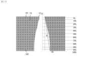
- FIG. 1 is a diagram showing a method for measuring the cross section and inclination angle of a through hole having a truncated cone shape.
- FIG. 2 is a diagram showing a method for measuring the side roughness of a through hole.
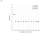
- FIG. 3 is a diagram showing the measurement results of the inclination angle of the through hole in Example 1 of the first embodiment.
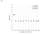
- FIG. 4 is a diagram showing the measurement results of the inclination angle of the through hole in Example 2 in the first embodiment.
- FIG. 5 is a diagram showing the measurement results of the inclination angle of the through hole in Example 3 in the first embodiment.
- FIG. 6 is a diagram showing a cross-sectional shape of a through hole of Comparative Example 1 in the first embodiment.
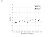
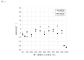
- FIG. 7 is a diagram showing the measurement results of the inclination angle of the through hole of Comparative Example 1 in the first embodiment.
- FIG. 8 is a diagram showing a cross-sectional shape of a through hole of Comparative Example 2 in the first embodiment.
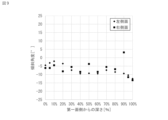
- FIG. 9 is a diagram showing the measurement results of the inclination angle of the through hole in Comparative Example 2 in the first embodiment.
- FIG. 10 is a diagram showing a cross-sectional shape of a through hole of Comparative Example 3 in the first embodiment.
- FIG. 11 is a diagram showing the measurement results of the inclination angle of the through hole in Comparative Example 3 in the first embodiment.
- FIG. 12 is a diagram showing the measurement results of the inclination angle of the through-hole in Application Example 1.
- FIG. 12 is a diagram showing the measurement results of the inclination angle of the through-hole in Application Example 1.
- FIG. 13 is a diagram showing the measurement results of the inclination angle of the through-hole in Application Example 2.
- FIG. 14 is a diagram showing the measurement results of the inclination angle of the through-hole in Application Example 3.
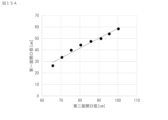
- FIG. 15A is a graph showing Table 5.
- FIG. 15B is a schematic diagram showing a case where a through electrode is formed.
- FIG. 15C is a diagram illustrating the characteristics of the through-holes and through-electrodes formed in the present disclosure.
- FIG. 16A is a diagram showing SEM images of typical cross-sectional shapes of through holes in each of the examples and comparative examples of the first embodiment.
- FIG. 16B is a diagram showing SEM images of cross sections of through holes in each of the examples and comparative examples according to the first embodiment.
- FIG. 16C is a diagram illustrating ridgelines of through holes in each example of the first embodiment.
- FIG. 16D is a diagram showing a case where a through electrode is formed in the through hole in the first embodiment.
- FIG. 17 is a diagram showing the transmission characteristics of the through electrode of Example 1 and the transmission characteristics of the through electrode of Comparative Example 1 in the first embodiment.
- FIG. 18 is a diagram showing an example of the configuration of a multilayer wiring board in the first embodiment.
- FIG. 19 is a diagram showing another example of the configuration of the multilayer wiring board in the first embodiment.
- FIG. 20 is a diagram showing a step of bonding a glass substrate to a first support.
- FIG. 21 is a diagram showing a process for forming a laser modified portion.
- FIG. 22 is a diagram showing a process of forming a first wiring layer.
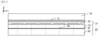
- FIG. 23 is a diagram showing a step of adhering a second support.
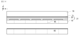
- FIG. 24 is a diagram showing a step of peeling off the first support.
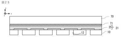
- FIG. 25 is a diagram showing a process of forming a through hole.
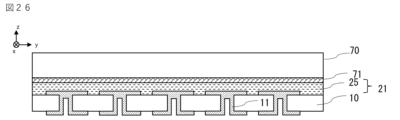
- FIG. 26 is a diagram showing a process of forming a through electrode.
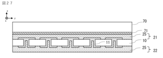
- FIG. 27 is a diagram showing a process of forming an insulating resin layer.
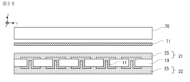
- FIG. 28 is a diagram showing a step of peeling off the second support and the second adhesive layer.
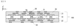
- FIG. 29 is a diagram showing a process of forming a first wiring layer and a second wiring layer.
- FIG. 30 is a diagram showing a case where a multi-layer wiring board is used as an interposer board for a semiconductor element and a BGA board.
- FIG. 31 is a diagram showing a cross section of the case of FIG.
- FIG. 32 is a diagram showing a case where a multilayer wiring board and a semiconductor element are used in an electronic device for communication.
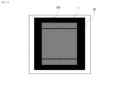
- FIG. 33 is a diagram showing a cross section of the case of FIG.
- the scope of the present invention is not limited to the exemplary embodiments and examples shown and described, but includes various modifications.
- the embodiments and examples in this disclosure have been described in detail to clearly explain the present invention, and are not necessarily limited to those having all the configurations described.
- the present invention also includes all embodiments that provide effects equivalent to those intended by the present invention.
- surface may refer not only to the surface of a plate-like member, but also to the interface of a layer contained in the plate-like member that is approximately parallel to the surface of the plate-like member. Additionally, “upper surface” and “lower surface” refer to the surface shown at the top or bottom of a drawing when a plate-like member or a layer contained in the plate-like member is illustrated. Additionally, the “upper surface” and “lower surface” may also be referred to as the “first surface” and the "second surface”.
- side surface refers to a surface of a plate-like member or a layer included in a plate-like member, or a portion of the thickness of a layer. Furthermore, a part of a surface and a side surface may be collectively referred to as an "end portion.” Furthermore, the “side surface of a through hole” refers to the interface on the object that forms the through hole when the through hole is provided in the object. In addition, “upper” refers to the vertically upward direction when a plate-like member or layer is placed horizontally.
- the distance in the Z-axis direction is referred to as the "height,” and the distance on the XY plane defined by the X-axis and Y-axis directions is referred to as the "width.”
- the term "through electrode provided in a glass substrate” refers to a conductive path provided to electrically connect the first and second surfaces of a glass substrate when the glass substrate is used as a part of a multilayer wiring substrate, and does not necessarily have to completely penetrate the glass substrate with a single conductive material. If the conductive path from the first surface and the conductive path from the second surface are connected, they are included in the through electrode.
- the form of the through electrode may be a filled type in which a through hole (including both a bottomed type and a completely through type) is filled with a conductive material, or a conformal type in which only the sidewall portion of the through hole is covered with a conductive material.
- planar shape and plan view refer to the shape of a surface or layer when viewed from above.
- cross-sectional shape and cross-sectional view refer to the shape of a plate-like member or layer when cut in a specific direction and viewed from the horizontal direction.
- central portion refers to the central portion other than the peripheral portion of a surface or layer, and the term “toward the center” refers to the direction from the peripheral portion of a surface or layer toward the center of the planar shape of the surface or layer.
- ⁇ Measurement method> In order to explain the shape of the through hole provided in the glass substrate according to the first embodiment of the present invention, first, a method for measuring the inclination angle of the through hole 12 and a method for measuring the side roughness will be described below.
- the results can be significantly different when observing the inclination angle of the sidewall at a certain position on the sidewall using a scale that overlooks the entire through hole in the glass substrate, compared to when the sidewall near the measurement point is enlarged to clearly show the minute irregularities on the sidewall at that position, and a precise determination is made as to where on that irregularity the point at which the angle was specified corresponds, and the inclination angle of the tangent at that position is used to determine the desired angle.
- the inclination angle of the glass substrate through hole in the present disclosure corresponds to the former, and means an inclination angle that reflects the tendency when the entire through hole is viewed from above, without being overly influenced by the unevenness of the side surface.
- One example of a measurement method is to set a tangent at a measurement point in a cross-sectional photograph taken at a scale and resolution that allows a bird's-eye view of the entire through hole and where minute irregularities on the side surface cannot be seen with the naked eye, so as to reflect as closely as possible the tendency of inclination at the measurement point and its vicinity.
- FIG. 1 is a diagram showing a method for measuring the cross section and inclination angle of the through hole 12 having a truncated cone shape.
- the cross section of the through hole 12 shown in FIG. 1 is obtained by cutting the through hole 12 from the first surface 101 side in the thickness direction of the glass substrate by a scriber to obtain a cross section (cut surface), and analyzing the SEM image observed by a SEM (Scanning Electron Microscope) using image analysis software.
- the area shown by the pattern pattern indicates the glass substrate 10.
- a truncated cone shape is formed on the first surface 101 side, and a truncated cone shape is also formed on the second surface 102 side, sandwiching the point having the minimum value.
- the scale of 5%, 10%, . . . 95% shown in FIG. 1 indicates the length from the first surface 101 to the second surface 102 of the glass substrate 10 as a percentage.
- a center line TC is drawn perpendicular to the first surface 101 at the center of the through hole 12 on the first surface 101 side of the glass substrate 10.
- the center line TC is translated toward either one of the two sides of the through hole 12 as shown by the arrow, and the translated center line TC is brought into contact with the point where the diameter of the through hole 12 is at its minimum value, and the point of contact is defined as a reference point RP.
- a tangent line ss is drawn at the cross-sectional position at each of the heights of the scale positions from 5% to 100% from the reference point RP, and the inclination angle of the tangent line ss is measured, and the inclination angle is defined as the inclination angle at each of the cross-sectional positions from 5% to 95%.
- the inclination angle is positive in the direction in which the diameter of the through hole 12 expands upward.
- the method for measuring the inclination angle includes steps (1) to (3): (1) creating a center line for the through hole 12, (2) moving the center line horizontally to a position where the opening is at its minimum to create a reference point, and (3) drawing a tangent line from the reference point to a specific position on the through hole to measure the angle.
- steps (1) to (3) (1) creating a center line for the through hole 12, (2) moving the center line horizontally to a position where the opening is at its minimum to create a reference point, and (3) drawing a tangent line from the reference point to a specific position on the through hole to measure the angle.
- a scribe and a precision breaker are used to cut (cut) the through hole 12 at the center from the first surface 101 side to expose the cross section of the through hole 12.
- a cutting method for example, three-point bending can be applied. After that, SEM observation is performed on the exposed cross section, and the angle of the through hole 12 is measured by image analysis of the SEM image of the cross section.
- the measurement range is usually the range from the first surface 101 to the second surface 102 of the through hole.
- two or more measurement ranges excluding the irregularities are set, and the results of the measurement ranges are averaged to determine the side roughness.
- FIG. 2 is a diagram showing a method for measuring the side roughness of a through hole.
- the through hole 12 shown in FIG. 2 has a general shape.
- FIG. 2(a) shows an SEM image of the cross section of the through hole 12.
- FIG. 2(b) shows a diagram in which the contour of the side of the through hole 12 is extracted from an SEM image obtained by observing the cross section of the through hole 12. Measurements of the average dispersion roughness and the unevenness width are carried out from the extracted contour data.
- FIG. 2(a) shows an SEM image of the cross section of the through hole 12.
- 2(c) is a diagram showing a formula for calculating the average dispersion roughness and the unevenness width.
- a roughness curve f(x) showing the roughness of the contour is measured in a set region L set based on the first surface 101.
- the average dispersion roughness (hereinafter also simply referred to as "dispersion roughness") Ra is obtained by integrating the absolute value of the roughness curve f(x) squared over the set region L and then dividing it by the length of the set region L, as shown in formula (1).
- the roughness width (hereinafter also referred to as "unevenness width”) a is the difference between the peak portion showing the maximum roughness value and the bottom portion showing the minimum roughness value in the roughness curve f(x).
- the average roughness of the through hole is calculated by averaging the roughness values calculated from them.
- the transmission characteristics are measured using the S parameter (S21), which indicates the frequency dependency of the degree of the propagating wave relative to the input wave.
- S21 is expressed as the logarithm of the power ratio (transmitted wave power/input wave power), and the smaller the absolute value, the smaller the transmission loss.
- a network analyzer was used to measure the S parameter (S21).
- a measurement sample was prepared by surrounding the periphery of the through electrode 11 formed on the glass substrate with a conductor and grounding the conductor, and S21 between the first surface 101 side and the second surface 102 side of the through electrode 11 was measured.
- the embodiment of the through hole 12 in the first embodiment will be described.
- etching is performed on the glass substrate 10 on which the laser modified portion 65 is formed from the second surface 102 side of the glass substrate 10. Therefore, the formed through hole 12 has a truncated cone shape whose diameter narrows from the second surface 102 toward the first surface 101.
- the inclination angle of the side surface of the through hole 12 changes depending on the laser processing conditions and etching conditions for the glass substrate 10.
- laser processing is performed on a glass substrate under irradiation conditions of the pulse width and number of shots shown in Table 1, and the through hole 12 is formed by subsequent etching.
- Example 1 of the first embodiment the pulse width is 5 ps and the number of shots is 1, in Example 2, the pulse width is 15 ps and the number of shots is 1, and in Example 3, the pulse width is 25 ps and the number of shots is 1.
- the comparative examples are through holes created by modifying the manufacturing method and laser processing method shown in the first embodiment. That is, in comparative example 1, the pulse width is 30 ps and the number of shots is 1, in comparative example 2, the pulse width is 30 ns and the number of shots is 50, and in comparative example 3, the pulse width is 50 ⁇ s and the number of shots is 5.
- the opening diameter on the second surface 102 side of the glass substrate 10 was 80 ⁇ m on average, and in this case, 3 ⁇ , which is the value obtained by adding three times the standard deviation to the average value of the measured values, was 4.5 ⁇ m or less.
- the difference between the maximum opening diameter ⁇ Max and the minimum opening diameter ⁇ Min was 10 ⁇ m or less.
- FIG. 3 is a diagram showing the measurement results of the inclination angle of the through hole in Example 1 of the first embodiment.
- FIG. 4 is a diagram showing the measurement results of the inclination angle of the through hole in Example 2 in the first embodiment.
- FIG. 5 is a diagram showing the measurement results of the inclination angle of the through hole in Example 3 in the first embodiment.
- FIG. 6 is a diagram showing a cross-sectional shape of a through hole of Comparative Example 1 in the first embodiment.
- FIG. 7 is a diagram showing the measurement results of the inclination angle of the through hole of Comparative Example 1 in the first embodiment.
- FIG. 8 is a diagram showing a cross-sectional shape of a through hole of Comparative Example 2 in the first embodiment.
- FIG. 9 is a diagram showing the measurement results of the inclination angle of the through hole in Comparative Example 2 in the first embodiment.
- FIG. 10 is a diagram showing a cross-sectional shape of a through hole of Comparative Example 3 in the first embodiment.
- FIG. 11 is a diagram showing the measurement results of the inclination angle of the through hole in Comparative Example 3 in the first embodiment.
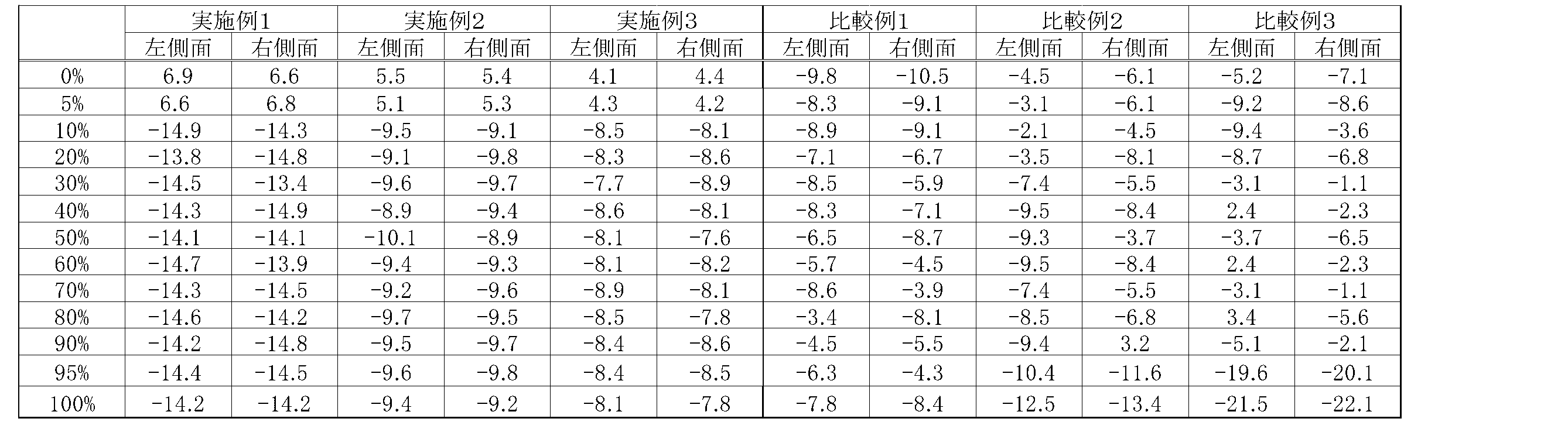
- Table 2 is a table showing the results of measuring the inclination angle of the side of the through hole 12 in each example of the embodiment and each comparative example. In each example of the embodiment, it is confirmed that there is a difference between the value of the side angle of the through hole 12 in the range of 0% to less than 10% of the distance from the first surface and the value in the range of 10% to 95% of the distance from the first surface.
- the side angle of the through hole 12 is almost constant in the range of 0% to less than 10% of the distance from the first surface (the side angle is in the range of 4° to 7°), and the side angle that is almost constant in the range of 10% to 95% of the distance from the first surface is in the range of -7° to -15°).
- the inclination angle of the side of the through hole 12 in the range of 95% to 100% of the distance from the first surface is the same as the inclination angle of the side of the through hole 12 in the range of 10% to 95% of the distance from the first surface, and the difference in the inclination angle between the two ranges is 1.0° or less.
- the inclination angle of the side surface of the through hole 12 varies at each position between 5% and 95% of the distance. It can be seen that the shapes of the inclination angles of the side surfaces of the through hole are significantly different between each of the examples of the present invention and the comparative examples.
- the average dispersion roughness and unevenness width of the side surface of the through hole 12 will be described for each example and each comparative example in the first embodiment with reference to Table 3.
- the dispersion roughness of the side surface shape at the cut surface of the through hole 12 in the thickness direction of the glass substrate is 1,000 nm or less and the unevenness width is 1,500 nm or less.
- the dispersion roughness is 1,500 nm or more and the unevenness width is 1,500 nm or more, confirming that there is a difference in the roughness of the side surface of the through hole.
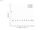
- Figs. 12 to 14 show the results of forming the inflection point of the side inclination angle of the through hole 12 in the range of 1% to 5% of the distance from the first surface as application examples of the first embodiment of the present invention.
- Fig. 12 is a diagram showing the measurement result of the inclination angle of the through hole in application example 1.
- Fig. 13 is a diagram showing the measurement result of the inclination angle of the through hole in application example 2.
- Fig. 14 is a diagram showing the measurement result of the inclination angle of the through hole in application example 3.
- Table 4 shows the measurement result of the inclination angle of the side of the through hole 12 in each application example.
- the etching process is performed by immersion treatment using a jet, but each application example is formed by switching the direction of the jet more slowly than each comparative example.
- the conditions of the number of pulses and the number of shots in each application example were the same as those in each example.
- the side angle of the through hole 12 is almost constant in the range of 0% to 5% of the distance from the first surface, and is almost constant in the range of 5% to 95% of the distance from the first surface.
- the inclination angle of the side of the through hole 12 in the range of 95% to 100% of the distance from the first surface is the same as the inclination angle of the side of the through hole 12 in the range of 10% to 95% of the distance from the first surface, and the difference in the inclination angle in the two ranges is 1.0° or less.
- the roughness of the side of the through hole is the same as that in Table 3, that is, the dispersion roughness is 1000 nm or less and the unevenness width is 1500 nm or less.
- Table 5 and FIG. 15A are used to explain the relationship between the opening diameters of the first and second surfaces of the through-hole according to the embodiment of the present invention.
- Table 5 shows the diameters of the openings on the first surface 101 and the second surface 102 of the through-hole 12 when the thickness of the glass substrate 10 is changed from 100 ⁇ m to 200 ⁇ m under the conditions of Example 1.
- FIG. 15A is a graph showing Table 5. According to the first embodiment, regardless of the opening diameter of the second surface 102, the relationship between the opening diameter of the second surface 102 and the opening diameter of the first surface 101 is first surface side opening diameter ⁇ 1/second surface side opening diameter ⁇ 2 ⁇ 0.4 or more.
- Table 6 shows the first surface opening diameter and second surface opening diameter for each example and each comparative example in the first embodiment.
- Table 6 shows typical values of the opening diameter ⁇ 1 on the first surface 101 side and the opening diameter ⁇ 2 on the second surface 102 side of the through hole 12 measured for each example and each comparative example in the first embodiment.
- FIG. 15B is a schematic diagram showing the case where a through electrode 12 is formed.
- the aperture diameter of the through hole 12 can be made smaller than ⁇ 2, as shown by the relationship ⁇ 1/ ⁇ 2 ⁇ 0.4.
- a coil is formed using the through electrode 11, and the relationship between ⁇ 1 and ⁇ 2 makes it possible to ensure the design freedom of the coil.
- the Q value can be reduced when a circuit including a coil is formed, making it possible to suppress transmission loss. As a result of the above, it is possible to stabilize the signal of the through electrode (reduce signal loss).
- FIG. 15C is a diagram for explaining the characteristics of the through hole and through electrode formed in the present disclosure.
- FIG. 15C is a diagram showing, for example, an enlarged view of region Ra in FIG. 29.
- a conductive electrode 31 can be formed directly on the through hole 12 (or the through electrode 11). This is because the through hole 12 has a so-called bottomed shape. By making it a bottomed shape, it is possible to form the conductive electrode 31 directly on the through hole 12. Therefore, the transmission distance of the electrode as a whole is shortened, and the transmission characteristics can be improved and the through hole 12 can be made finer.
- the side surface of the through hole 12 in the present disclosure has no inflection point at which the side shape changes, and the surface is smooth. Therefore, when plating is performed on the through hole 12, a uniform metal film or the like can be formed, so that the generation of parasitic capacitance can be suppressed on the side surface of the through hole 12.
- the shape of the through hole 12 can be a shape having an inflection point or a so-called straight shape in which the diameter hardly changes from the first surface to the second surface of the glass substrate, but from the viewpoint of transmission characteristics, the shape shown in the present disclosure that can suppress the generation of parasitic capacitance is desirable.
- Figures 16A to 16D are diagrams for explaining the side of the through hole in each example and comparative example.
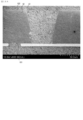
- Figure 16A is a diagram showing an SEM image of a typical cross-sectional shape of the through hole in each example and comparative example in the first embodiment.
- the SEM images were taken of the cut surface of the through hole in the thickness direction of the glass substrate.
- the SEM images shown in Figures 16A to 16D were taken at a magnification of 1000 times (one division of the scale is 5 ⁇ m).
- 16A in order to easily observe the cross-sectional shape of the glass substrate according to the first embodiment, the through-hole 12 is filled with a resin material. It can be seen that the inclination angle of the side surface changes from the first surface 101 toward the second surface 102.
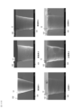
- 16B is a diagram showing SEM images of the cross-sectional shapes of the through-holes of each example and each comparative example in the first embodiment.
- the inclination angle and cross-sectional shape are different from those described above, but the pulse width and shot number conditions are as described in each example and each comparative example.
- the appearance of the SEM image and the smoothness of the cross section of the through-hole have common properties.
- the areas that have high contrast and appear white are areas where the angle of the inclined surface of the sample changes and become the ridges of the inclined surface.
- the areas that appear as white lines indicate the peaks or bottoms of the roughness of the sample surface, and the roughness of the side surface of the through hole, which affects the transmission characteristics of the through electrode, can be grasped based on the presence and degree of arrangement of the ridges formed on the side surface of these through holes.
- FIG. 16C is a diagram for explaining the ridge lines of the through holes of each example in the first embodiment.
- Fig. 16C(a) is an enlarged view of Example 3 of Fig. 16B.
- Fig. 16C(b) is a diagram showing the ridge lines of the side and cross section of the through hole observed in the SEM image by solid lines. In the example shown in Fig.
- the interval between the ridge lines is the widest among the substantially parallel ridge lines between ridge lines Rl1 and Rl2.
- the interval between the ridge lines on the side surface in the direction perpendicular to the first surface 101 is equal to or less than Rs.
- the interval between the ridge lines is equal to or less than 15.5 ⁇ m.
- the frequency of ridgelines extending in a direction perpendicular to the first surface 101 and white lines extending in a direction between the direction parallel to the first surface 101 and the direction perpendicular to the first surface 101 increases.
- the proportion of ridgelines extending vertically and ridgelines extending diagonally decreases as the dispersion roughness decreases.
- white lines extending in a direction between the direction parallel to the first surface 101 and the direction perpendicular to the first surface 101 i.e., diagonal direction
- 16D is a diagram showing an SEM image of a cross section when a through electrode is formed in the through hole in the first embodiment.
- the inclination angle and cross section shape are different from those described above, but the pulse width and the number of shots are as described in each example and each comparative example.
- the appearance of the SEM image and the smoothness of the cross section of the through hole have common properties.
- the area indicated by the arrow and surrounded by the dashed line has a shape with a rising edge.
- the side surface of the through hole 12 and the second surface 102 of the glass substrate 10 have a shape with a rising edge, and the side surface and the second surface region can be clearly distinguished in a 1000x SEM image.
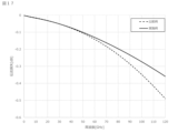
- FIG. 17 is a diagram showing the transmission characteristics of the through electrodes of Example 1 in the first embodiment and the transmission characteristics of the through electrodes of Comparative Example 1.
- FIG. 17 shows the results of measuring the transmission loss S21 as the transmission characteristics in the through electrodes. Since Examples 1 to 3 showed the same tendency in the transmission characteristics, Example 1 is shown as a representative. Furthermore, since Comparative Examples 1 to 3 showed almost the same tendency in the transmission characteristics, Comparative Example 1 is shown as a representative. The formation conditions of the seed layer for forming the electrode and the plating process were the same for both the examples and the comparative examples. As shown in FIG.
- the transmission loss of the examples is smaller than the transmission loss of the comparative examples in any frequency range. Therefore, it can be seen that the smaller the values of the dispersion roughness and the unevenness width are for the side surface of the through hole, the smaller the loss in the through electrode formed in the through hole, and the better the transmission characteristics are.
- the transmission characteristic S21 was also measured for each example and each comparative example when the thickness of the glass substrate 10 was changed. The results are shown in Table 6. As shown in Table 7, the thickness of the glass substrate 10 was set to 100 ⁇ m, 150 ⁇ m, and 200 ⁇ m, and through holes and through electrodes were created under conditions based on each example and each comparative example, and the transmission characteristics were measured. As shown in Table 7, it is confirmed that the examples in the first embodiment show better transmission characteristic S21 values than the comparative examples.
- the transmission characteristics shown in Table 7 are those of a single through electrode, and in a multilayer wiring board that requires multiple through electrodes, improving the transmission characteristics of a single through electrode leads to a significant performance improvement.
- the through electrodes shown in Examples 1 to 3 have achieved better results than the through electrodes shown in Comparative Examples 1 to 3. Comparing the Examples, it can be said that Example 1 is the most preferable, followed by Example 2 and Example 3.
- the reliability evaluation results by the TCT test are shown in Tables 8 and 9.
- the reliability test conditions are as follows: Setting conditions: Lower limit temperature was -40°C/30 minutes, and upper limit temperature was 150°C/30 minutes.
- ⁇ Test equipment TSA-43EL manufactured by Espec
- NG criteria If the resistance value after cycling is more than 10 times the initial resistance value, it is judged as NG.
- each example relating to an embodiment of the present invention shows higher reliability than each comparative example.
- FIG. 18 is a diagram showing an example of the configuration of the multilayer wiring board 1 in the first embodiment.
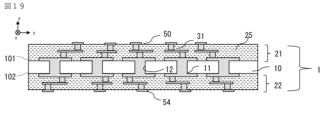
- FIG. 19 is a diagram showing another example of the configuration of the multilayer wiring board 1 in the first embodiment.
- the multilayer wiring board 1 includes a glass substrate 10, a first wiring layer 21, and a second wiring layer 22.
- the first wiring layer 21 is disposed on the first surface 101 side of the glass substrate 10, and the second wiring layer 22 is disposed on the second surface 102 side of the glass substrate 10.
- the glass substrate 10 includes a through hole 12 penetrating from the first surface 101 side to the second surface 102 side.
- the through electrode 11 is formed by a conductor formed along the side surface of the through hole 12.
- the through electrode 11 electrically connects a part of the first wiring layer 21 and a part of the second wiring layer 22.
- the first wiring layer 21 and the second wiring layer 22 include an insulating resin layer 25.
- the first wiring layer 21 and the second wiring layer 22 may be configured by stacking a plurality of layers, and the number of layers may be set as necessary.
- the through electrode 11 is an electrode for establishing an electrical connection between the first wiring layer 21 and the second wiring layer 22.
- the conductive electrodes 31 are electrodes for ensuring electrical continuity in the thickness direction of the multilayer wiring board 1.
- the semiconductor element bonding pads 50 are members for connecting a semiconductor circuit to be mounted on the multilayer wiring board 1.
- the board bonding pads 54 are members for bonding the multilayer wiring board 1 to another board.
- a conductor may be placed only on the side of the through hole 12 as shown in FIG. 18, or a conductor may be embedded in the through hole 12 as shown in FIG. 19.
- the conduction electrode 31 it is possible to arrange the conduction electrode 31 above the through electrode 11 of the first wiring layer 21 in the Z-axis direction.
- the thickness of the multilayer wiring board 1 is, for example, in the range of 100 ⁇ m to 400 ⁇ m.
- a method for manufacturing the multilayer wiring board 1 will be described with reference to Figures 3 to 12. First, a process for forming the through holes 12 in the glass substrate 10 will be described.
- FIG. 20 is a diagram showing a process of bonding the glass substrate 10 to the first support 62. As shown in FIG. The thickness of the glass substrate 10 can be appropriately set depending on the application, taking into consideration the thickness after etching.
- a first support 62 is bonded to a glass substrate 10 via a first adhesive layer 61, forming a laminated structure 63 including the glass substrate 10, the first adhesive layer 61, and the first support 62.
- the glass substrate 10 and the first support 62 are temporarily fixed by a first adhesive layer 61 .
- a laminator, a vacuum pressure press, a reduced pressure bonding machine, or the like can be used.
- the first support 62 is desirably made of, for example, the same material as the glass substrate 10.
- the first support 62 is desirably made of alkali-free glass.
- the thickness of the first support 62 can be appropriately set according to the thickness of the glass substrate 10. However, it is desirably a thickness that allows transport during the manufacturing process, and the thickness of the support is, for example, in the range of 300 ⁇ m to 1,500 ⁇ m.
- alkali-free glass having a SiO 2 ratio in the range of 55% by mass to 81% by mass can be used. If the SiO 2 ratio of the glass substrate 10 is greater than 81% by mass, the etching processing speed decreases, the side angle of the through hole 12 decreases, and poor adhesion occurs when forming the through electrode 11 described later. In addition, if the SiO 2 ratio is less than 55% by mass, there is a high possibility that alkali metals will be contained in the glass, which will affect the reliability of the multilayer wiring substrate after mounting the electronic device. If the SiO 2 ratio of the alkali-free glass is greater than 55% by mass to 81% by mass, the set ratio may be set appropriately.
- [Laser modification process] 21 is a diagram showing a process of forming a laser modified portion.
- a laser modified portion 65 is formed on the glass substrate 10.
- the laser modified portion 65 is processed into a shape of ⁇ 3 ⁇ m or less on the glass substrate 10, and is continuously formed in the thickness direction of the glass substrate 10. At this time, it is desirable that minute cracks (hereinafter also referred to as "microcracks") of 5 ⁇ m or more do not occur around the laser modified portion 65.
- the dispersion roughness on the side of the through hole 12 after etching will be 1000 nm or more and the unevenness width will be 1500 nm or more, making it difficult to obtain a through hole 12 with a smooth side.
- microcracks of 5 ⁇ m or more occur, as described later, roughness that changes at intervals will occur on the side of the through hole 12 after etching in a direction perpendicular to the first surface 101 of the glass substrate 10.
- the laser modified portion 65 For processing the laser modified portion 65, it is preferable to use, for example, a femtosecond laser or a picosecond laser, and to use a laser oscillation wavelength of one of 1064 nm, 532 nm, or 355 nm. If the laser pulse width is 25 picoseconds or more, microcracks of 5 ⁇ m or more tend to occur around the laser modified portion 65, so it is preferable that the laser pulse width is 25 picoseconds or less. In addition, since microcracks tend to occur when processing is performed by multiple pulse irradiation, it is preferable to form the laser modified portion 65 with one pulse.
- the laser oscillation wavelength and laser output may be appropriately set according to the thickness of the glass substrate 10.
- a laser is irradiated to the glass substrate at the portion where the through hole is to be formed, and the maximum length of the microcracks that occur around the laser irradiation is 5 ⁇ m.
- FIG. 22 is a diagram showing a process of forming the first wiring layer 21.
- the first wiring layer 21 made of a conductive layer and an insulating resin layer is formed on the first surface 101 on the glass substrate 10 of the laminated structure 63.
- the through electrode connection portion 41 (or wiring between the through electrodes) is formed on the first surface 101 by a semi-additive (SAP) process.
- SAP semi-additive
- the hydrofluoric acid resistant metal layer on the glass substrate 10 is an alloy layer containing chromium, nickel, or both, and can be formed in the range of 10 nm to 1,000 nm by sputtering. Then, a conductive metal film is formed on the hydrofluoric acid resistant metal with a desired thickness.
- the conductive metal film can be appropriately selected from, for example, Cu, Ni, Al, Ti, Cr, Mo, W, Ta, Au, Ir, Ru, Pd, Pt, AlSi, AlSiCu, AlCu, NiFe, ITO, IZO, AZO, ZnO, PZT, TiN, and Cu 3 N 4 .
- a photoresist is used to form the desired pattern in order to form a wiring pattern by plating.
- a dry film resist is used, but liquid resist can also be used.
- a plating film is formed by electrolytic plating, the unnecessary resist is peeled off, and the seed layer is etched to form the wiring.
- the insulating resin layer 25 is a thermosetting resin, and the material thereof is a material containing at least one of an epoxy resin, a polyimide resin, and a polyamide resin, and containing a silica SiO2 filler.
- the material of the insulating resin layer 25 can be appropriately selected according to need. However, when a photosensitive insulating resin material is used, it becomes difficult to fill the silica SiO2 filler in order to ensure photolithography properties, so although a photosensitive insulating resin material can also be used, it is more preferable to use a thermosetting resin.
- [Second support bonding step] 23 is a diagram showing a step of adhering a second support body.
- a second adhesive layer 71 is formed on the first wiring layer 21 of the laminated structure 63, and a second support body 70 is disposed on the second adhesive layer 71 and adhered thereto.
- the second support 70 may be made of, for example, glass, and is preferably made of the same material as the glass substrate 10.
- the second support 70 is preferably made of alkali-free glass.
- the thickness of the second support 70 can be appropriately set depending on the thickness of the glass substrate 10. However, it is preferable that the thickness be such that the second support 70 can be transported, and the range of this thickness is from 300 ⁇ m to 1,500 ⁇ m.
- [Peeling process] 24 is a diagram showing a step of peeling off the first support 62. As shown in FIG. 24, the glass substrate 10 and the first support 62 are peeled off at the first adhesive layer 61.
- FIG. 25 is a diagram showing a process of forming the through holes 12. As shown in FIG.
- the glass substrate 10 on which the laser modified portion 65 is formed is subjected to an etching process using a predetermined etching solution, thereby forming the through hole 12.
- the second surface of the glass substrate 10 is also etched, and the thickness of the glass substrate 10 is reduced. The etching is performed from the second surface 102 side of the glass substrate 10.
- the etching solution contains hydrofluoric acid in the range of 0.2 mass% to 20.0 mass%, nitric acid in the range of 4.0 mass% to 25.0 mass%, and inorganic acid other than hydrofluoric acid and nitric acid in the range of 0.5 mass% to 11.0 mass%.
- inorganic acids other than hydrofluoric acid and nitric acid include hydrochloric acid, sulfuric acid, phosphoric acid, and sulfamic acid, and at least one inorganic acid is contained depending on the type of components other than silicon contained in the glass substrate 10.
- the etching solution contains hydrochloric acid and sulfuric acid, and the etching rate for the glass substrate 10 is appropriately adjusted to be in the range of 0.1 ⁇ m/min to 10 ⁇ m/min.
- the etching rate for the glass substrate 10 is preferably in the range of 0.25 ⁇ m/min to 4 ⁇ m/min, and more preferably in the range of 0.25 ⁇ m/min to 0.5 ⁇ m/min.
- the etching temperature is not particularly limited and can be appropriately adjusted, but is, for example, in the range of 10°C to 30°C.
- etching is performed by immersion processing using a jet or spray processing to form the through-hole 12.
- immersion processing using a jet for example, in order to efficiently etch the bottom of the through-hole 12, the direction of the jet is switched in the etching solution.
- pressure is applied to the bottom of the through-hole 12, and it is possible to change the inclination angle of the TGV side at a position 1 to 10% away from the first surface.
- etching process by spray processing by setting the oscillation speed of the spray having an injection port for injecting the etching solution or the oscillation speed of the substrate quickly, pressure is applied to the bottom of the through-hole 12, and it is possible to change the inclination angle of the TGV side at a position 1% to 10% away from the first surface.
- the processing conditions vary depending on the size of the device used, it is desirable to set the processing conditions after confirming the shape of the through hole 12.
- ultrasonic waves or the like may be used in combination as another mechanism.
- FIG. 26 is a diagram showing a process for forming the through electrodes 11.
- a metal layer for electrolytic plating is formed on the second surface 102 of the glass substrate 10 in which the through-hole 12 is formed.
- the metal layer may be any metal that functions as a seed layer for electrolytic plating, such as metals including Cu, Ti, Cr, W, Ni, etc. At least one of the above metals is used for the metal layer, and it is preferable that a Cu layer is formed on the outermost surface of the metal layer. It is preferable that Ti, Cr, W, and Ni are used as an adhesive layer with the glass substrate 10 below the Cu layer.
- the thickness of the metal layer is appropriately set to a range that can cover the side of the through-hole 12. As a formation method, for example, a deposition formation method using sputtering can be adopted.
- the through electrode 11 is formed by electrolytic plating using the metal layer as a seed layer.
- a mask is formed on the second surface 102 of the glass substrate 10 in the through hole 12 and a predetermined area around the through hole 12 using an insulator such as resist, and then electrolytic plating is performed.
- a material used for electrolytic plating for example, Cu can be used, and other metals including Au, Ag, Pt, Ni, Sn, etc. can also be used.
- electrolytic plating may be performed so that the inside of the through hole 12 is filled with a conductor such as the above metal.
- FIG. 27 is a diagram showing the process of forming the insulating resin layer. After the electrolytic plating process for forming the through electrodes is performed, the insulator such as resist is removed, and the metal film that served as the seed layer formed on the second surface 102 of the glass substrate 10 is removed. After each of the multiple through electrodes 11 formed on the glass substrate 10 is electrically isolated, the insulating resin layer 25 is formed on the second surface side as shown in FIG. 27.
- Fig. 28 is a diagram showing the step of peeling off the second support 70 and the second adhesive layer 71.
- the second adhesive layer 71 and the second support 70 formed above the first wiring layer 21 are peeled off from the interface between the first wiring layer 21 and the second adhesive layer 71 on the first surface 101 side.
- a glass substrate 10 is obtained in a state in which the first wiring layer 21 is formed on the first surface 101 side and the second wiring layer 22 is formed on the second surface 102 side.
- a peeling method according to the material used can be appropriately selected from UV light irradiation, heat treatment, physical peeling, etc., depending on the material used in the second adhesive layer 71. Furthermore, if a residue of the second adhesive layer 71 remains on the bonding surface between the first wiring layer 21 and the second adhesive layer 71, plasma cleaning, ultrasonic cleaning, water washing, solvent cleaning using alcohol, etc. may be performed.
- FIG. 29 is a diagram showing a process of forming the first wiring layer 21 and the second wiring layer 22.
- the first wiring layer 21 is formed on the first surface 101
- the second wiring layer 22 is formed on the second surface 102.
- a mask having a pattern is formed by a photosensitive resist or a dry film resist, and then wiring is formed by electrolytic plating.
- the insulating resin layer 25 is laminated.
- a hole is formed in the insulating resin layer 25 by laser processing or the like, and then a metal film is formed by electroless plating or deposition treatment by sputtering.
- a mask having a pattern is formed on the above-mentioned metal film using a resist, and a conductor is filled in the hole formed by electrolytic plating. Then, the mask and the excess metal film are removed. The above process is repeated multiple times according to the required number of layers to form the first wiring layer 21 and the second wiring layer 22.
- the first wiring layer 21 and the second wiring layer 22 have the same number of layers in order to suppress warping of the multilayer wiring board 1.
- the number of layers of the first wiring layer 21 and the second wiring layer 22 may be different.
- the number of layers of the first wiring layer 21 and the number of layers of the second wiring layer 22 may be set appropriately depending on the application of the multilayer wiring board.
- Second Embodiment Fig. 30 is a diagram showing a case where a multilayer wiring board 1 is used as an interposer board for a semiconductor element 100 and a BGA (Ball Grid Array) board 90.
- Fig. 31 is a diagram showing a cross section in the case of Fig. 30.
- Fig. 32 is a diagram showing a case where a multilayer wiring board 1 and a semiconductor element 100 are used in an electronic device for communication.
- Fig. 33 is a diagram showing a cross section in the case of Fig. 32.
- the electronic device used has a layer thickness of 800 ⁇ m or less. The applications of the above electronic devices are limited due to the influence of the transmission characteristics of the through electrodes, but the use of a multilayer wiring board using the glass substrate of the present invention makes it possible to apply electronic devices to high frequency band regions.
- a glass substrate having a first surface and a second surface, and at least one through hole extending from the first surface to the second surface,
- the side surface of the through hole is within a distance range of 0% or more and less than 10% from the first surface, the angle of the side surface is in a range of 4° or more and 7° or less, and when the side surfaces of the through hole are a left side surface and a right side surface in a cross-sectional view, the difference between the inclination angle of the left side surface and the inclination angle of the right side surface is 1.0° or less, Within a distance range of 10% or more and 100% or less from the first surface, the angle of the side surface is in a range of -7° or more and -15° or less, and the difference between the inclination angle of the left side surface and the inclination angle of the right side surface is 1.0° or less.
- a glass substrate according to any one of aspects 1 to 4 The distributed roughness is an arithmetic average roughness calculated by extracting a roughness curve based on the profile data of the side surface, setting a set interval on the roughness curve, and calculating the arithmetic average roughness in the set interval using Equation 1, A glass substrate, wherein the unevenness width is the difference between the highest part and the lowest part in the set section.
- the SiO2 ratio of the glass substrate is in the range of 55% by mass or more and 81% by mass or less.
- a multilayer wiring substrate comprising the glass substrate according to any one of aspects 1 to 6,
- the thickness of the electronic device mounted on the multilayer wiring board is 800 ⁇ m or less;
- the multilayer wiring board has a thickness of 100 ⁇ m or more and 400 ⁇ m or less.
- a method for producing a glass substrate according to any one of aspects 1 to 7, comprising the steps of: A first step of irradiating a laser onto a portion of a glass substrate where a through hole is to be formed; a second step of etching the glass substrate irradiated with a laser to form a through hole.
- the second step is a step of immersing the laser-irradiated glass substrate in an etching solution, and performing an etching process in which a jet direction of the etching solution is changed to form a through hole.
- Multilayer wiring board 10: Glass substrate, 11: Through electrode, 12: Through hole, 21: First wiring layer, 22: Second wiring layer, 25: Insulating resin layer, 31: Conductive electrode, 50: Bonding pad for semiconductor element, 54: Bonding pad for substrate, 61: First adhesive layer, 62: First support, 63: Laminated structure, 65: Laser modified part, 70: Second support, 71: Second adhesive layer, 90: BGA substrate, 100: Semiconductor element, 101: First surface of glass substrate 10, 102: Second surface of glass substrate 10, TC: Center line of through hole, ss: Tangent to the side of the through hole
Landscapes
- Engineering & Computer Science (AREA)
- Microelectronics & Electronic Packaging (AREA)
- Manufacturing & Machinery (AREA)
- Chemical & Material Sciences (AREA)
- Inorganic Chemistry (AREA)
- Chemical Kinetics & Catalysis (AREA)
- General Chemical & Material Sciences (AREA)
- Physics & Mathematics (AREA)
- Optics & Photonics (AREA)
- Ceramic Engineering (AREA)
- Internal Circuitry In Semiconductor Integrated Circuit Devices (AREA)
- Production Of Multi-Layered Print Wiring Board (AREA)
- Structure Of Printed Boards (AREA)
- Printing Elements For Providing Electric Connections Between Printed Circuits (AREA)
- Laser Beam Processing (AREA)
Abstract
Description
しかし、従来技術においては、熱応力に対する貫通電極の信頼性を高めるための貫通孔御形状について、十分に検討がされていないことから、貫通電極と配線層の界面で配線層が破断することが確認されている
上記した以外の課題、構成および効果は、以下の発明を実施するための形態における説明により明らかにされる。
さらに、本発明が目的とするものと均等な効果をもたらす全ての実施形態をも含むものである。
また、「貫通孔の側面」とは、物体に設けられた貫通孔について、貫通孔を形成している物体上の界面を意味する。
また、「上方」とは、板状部材又は層を水平に載置した場合の垂直上方の方向を意味する。さらに、「上方」及びこれと反対の「下方」については、これらを「Z軸プラス方向」、「Z軸マイナス方向」ということがあり、水平方向については、「X軸方向」、「Y軸方向」ということがある。
また、「ガラス基板に設けた貫通電極」とは、ガラス基板を多層配線基板の一部として用いる場合に、ガラス基板の第1面及び第二面を電気的に導通するために設けた導電経路を意味し、必ずしも、ガラス基板を単一の導電材料で完全に貫通している必要はない。第1面からの導電通路と第二面からの導電通路が接続されていれば、貫通電極に含まれる。さらに、貫通電極の形態は、貫通孔(有底のものも、完全な貫通のものも、いずれの形態をも含む)を導電材料で埋め込んだフィルド型でもよいし、貫通孔の側壁部分のみを導電材料で覆ったコンフォーマルのいずれをも含む。
さらに、「中心部」とは、面又は層の周辺部ではない中心部を意味する。そして、「中心方向」とは、面又は層の周辺部から面又は層の平面形状における中心に向かう方向を意味する。
本発明の第一実施形態に係るガラス基板に設けた貫通孔の形状を説明するために、まず、貫通孔12の傾斜角度の測定方法、側面粗さの測定方法を以下に示す。
貫通孔における特定の位置を、ガラス基板の片面からの深さ方向の位置で指定した場合、その位置での側面の角度は、その位置での側面表面の形状をどの程度のスケールにて観察するかに大きく依存する。
つまり、ガラス基板の貫通孔全体を俯瞰するようなスケールにて、側壁のある位置での側壁の傾斜角を観察した場合と、測定点付近の側壁を拡大し、その位置での側壁の微小な凹凸が明瞭となり、角度を指定した点が、その凹凸のどこに相当するかを厳密に判定して、その位置での接線の傾斜角をもって、目的の角度とする場合とでは、結果が大きく異なる可能性がある。
本開示におけるガラス基板貫通孔の傾斜角とは、前者にあたるものであり、側面表面の凹凸に過度に影響されることなく、貫通孔全体を俯瞰的に見た場合の傾向を反映した傾斜角を意味する。
測定法の一例として、貫通孔全体が俯瞰でき、かつ、側面の表面の微細な凹凸が目視できないスケール、解像度での断面写真において、測定点およびその近傍での傾斜の傾向をできるだけ反映するように測定点における接線を設定することが挙げられる。
まず、図1に本発明の第一実施形態で得られる貫通孔12の形状を説明している。図1は、円錐台形状の貫通孔12の断面および傾斜角度の測定方法を示す図である。図1に示される貫通孔12の断面は、貫通孔12を第一面101側より、ガラス基板の厚さ方向においてスクライブにて割断(裁断)して断面(裁断面)を出し、SEM(Scanning Electron Microscope:走査電子顕微鏡)によって観察されたSEM画像を画像解析ソフトを使用して解析したものである。図1において、パターン模様で示した箇所がガラス基板10を示している。図1に示す貫通孔12は、貫通孔12は第一面101と第二面102の間に貫通孔の径が極小となる極小値を持つ。極小値を持つ点を挟んで、第一面101側には円錐台形状が形成され、第二面102側にも円錐台形状が形成されている。なお、図1に示される目盛り5%、10%、・・・95%は、ガラス基板10の第一面101から第二面102までの長さを割合で示している。
ガラス基板10の第一面101側の貫通孔12の中心部に、第一面101と垂直になるように中心線TCを引く。次に、矢印に示されるように中心線TCを貫通孔12の両側のいずれか一方に向かって平行移動させ、平行移動させた中心線TCが貫通孔12の径が極小値を取る点と接触させ、接触させた点を基準点RPとする。そして、基準点RPから5%から100%のそれぞれの目盛り位置の高さの断面の位置に接線ssを引き、接線ssの傾斜角度を測定し、その傾斜角度を、5%から95%のそれぞれの断面の位置における傾斜角度であるとする。傾斜角度は、貫通孔12の径が上方に向けて広がる方向を正とする。
続いて、貫通孔12の側面粗さの測定方法について説明する。貫通孔12の側面粗さに測定については、側面角度の測定と同様に貫通孔12の断面をSEMによって観察し、観察されたSEM画像を画像解析ソフトを使用して解析する。貫通孔の側面粗さを計測するためには、通常は、貫通孔の第一面101から第二面102に至る範囲を測定範囲とする。ただし、仮に、貫通孔に凹凸が存在している場合には、当該凹凸部を除いた範囲を2つ以上の測定範囲として設定し、それらの測定範囲の結果を平均して側面粗さとする。また、側面粗さの算出に当たっては、同じ条件で作成した貫通孔5つ(サンプル数n=5)について、同様の測定を行い、これらの平均値を当該条件で作成した貫通孔の側面粗さとして規定する。
図2は、貫通孔の側面粗さの測定方法を示す図である。図2に示す貫通孔12は、説明のため、一般的な形状のものを掲載している。図2(a)は、貫通孔12の断面のSEM画像を示す。図2(b)は、貫通孔12の断面を観察したSEM画像より、貫通孔12の側面の輪郭を抽出した図を示す。抽出された輪郭データより平均分散粗さおよび凹凸巾の測定を実施する。図2(c)は、平均分散粗さの計算式および凹凸巾を模式的に示す図である。図2(b)において抽出された輪郭データに関し、第一面101を基準として設定した設定領域Lにおいて、輪郭の粗さを示す粗さ曲線f(x)を測定する。平均分散粗さ(以下、単に「分散粗さ」ともいう。)Raは、式(1)に示されるように、粗さ曲線f(x)の絶対値を2乗したものを、設定領域Lにわたって積分したうえで設定領域Lの長さで割ったものである。また、ラフネス幅(以下、「凹凸巾」ともいう。)aは、粗さ曲線f(x)のうち、粗さの最大値を示すピーク部と粗さの最小値を示すボトム部との差である。
なお、一つ貫通孔において、複数の粗さ曲線f(x)が設定された場合には、それらから算出された粗さの値の平均値によって当該貫通孔の平均粗さを算出することとなる。
伝送特性の測定には、入力波に対する伝搬波の度合いの周波数依存性を示すSパラメータ(S21)を用いる。S21は電力比(透過波電力/入力波電力)の対数で表され、絶対値が小さいほうが伝送損失が小さいことを示す。
Sパラメータ(S21)の測定にはネットワークアナライザを用いた。測定サンプルとしては、ガラス基板に形成した貫通電極11の周辺を導体で囲み、導体を接地した状態としたものを作製し、これによって、貫通電極11の第一面101側から第二面102側の間におけるS21を測定した。
第一実施形態における貫通孔12に実施形状について説明する。実施形態では、後述する図25に示されるように、レーザ改質部65が形成されたガラス基板10に対して、ガラス基板10の第二面102側からエッチングが行われる。このため、形成された貫通孔12は、第二面102から第一面101に向かって径が窄まる円錐台形状を有する。貫通孔12の側面の傾斜角度は、ガラス基板10に対するレーザ加工条件、エッチング条件よって変化する。
本発明の各実施例では、表1に示すパルス幅およびショット数の照射条件によってガラス基板にレーザ加工を行い、その後のエッチングにより貫通孔12を形成している。第一実施形態における実施例1においてはパルス幅が5psかつショット数が1、実施例2においてはパルス幅が15psかつショット数が1、実施例3においてはパルス幅が25psかつショット数が1である。
また、比較例は、第一実施形態に示した製造方法とレーザ加工方法を変更して作成した貫通孔である。つまり、比較例1においてはパルス幅が30psかつショット数が1、比較例2においてはパルス幅が30nsかつショット数が50、比較例3においてはパルス幅が50μsかつショット数が5である。
なお、各実施例および各比較例のいずれについても、ガラス基板10の第二面102側の開口径は平均80μmであり、この場合、計測値の平均値に標準偏差の3倍を加えた値である3σは4.5μm以下であった。また、形成されたレーザ改質部65の第二面102における開口径について、開口径の最大値φMaxと最小値φMinの差は10μm以下であった。

以下、図3から図23を参照して、第一実施形態における各実施例、比較例の貫通孔の形状、特性形状を説明する。
図3は、第一実施形態における実施例1の貫通孔の傾斜角度の測定結果を示す図である。
図4は、第一実施形態における実施例2の貫通孔の傾斜角度の測定結果を示す図である。
図5は、第一実施形態における実施例3の貫通孔の傾斜角度の測定結果を示す図である。
図6は、第一実施形態における比較例1の貫通孔の断面形状を示す図である。
図7は、第一実施形態における比較例1の貫通孔の傾斜角度の測定結果を示す図である。
図8は、第一実施形態における比較例2の貫通孔の断面形状を示す図である。
図9は、第一実施形態における比較例2の貫通孔の傾斜角度の測定結果を示す図である。
図10は、第一実施形態における比較例3の貫通孔の断面形状を示す図である。
図11は、第一実施形態における比較例3の貫通孔の傾斜角度の測定結果を示す図である。
表2は、実施形態の各実施例および各比較例における貫通孔12の側面の傾斜角度を測定した結果を表形式に取りまとめたものである。実施形態に係る各実施例では、貫通孔12に側面角度が第一面からの距離0%以上10%未満の範囲における値と、第一面からの距離10%以上95%以下の範囲における値との間に、差があることが確認されている。言い換えると、貫通孔12に側面角度が第一面からの距離0%以上10%未満の範囲においてほぼ一定であり(側面の角度は4°以上7°以下の範囲となり)、第一面からの距離10%以上95%以下の範囲においてほぼ一定となる側面の角度は-7°以上-15°以下の範囲となる)ことが確認される。また、第一面からの距離95%以上100%以下の範囲における貫通孔12の側面の傾斜角度は、第一面からの距離10%以上95%以下の範囲における貫通孔12の側面の傾斜角度と同等の傾斜角度となり、2つの範囲における傾斜角度の差が1.0°以下となる。
各比較例では、距離5%以上95%以下の各位置で貫通孔12の側面の傾斜角度がばらつくことがわかる。本発明の各実施例と比較例では貫通孔の側面の傾斜角度の形状が大きく異なることがわかる。
次に、表3を用いて第一実施形態における各実施例および各比較例に関し貫通孔12の側面の平均分散粗さおよび凹凸巾について説明する。表3に示されるように、第一各実施例では、ガラス基板の厚さ方向における貫通孔12の裁断面における側面形状の分散粗さが1,000nm以下かつ凹凸巾が1,500nm以下となる。各比較例では、分散粗さが1,500nm以上かつ凹凸巾が1,500nm以上となり、貫通孔側面の粗さに差があることが確認されている。

各応用例では、貫通孔12に側面角度が第一面からの距離0%から5%の範囲においてほぼ一定であり、第一面からの距離5%から95%の範囲においてほぼ一定となることが確認された。また、第一面からの距離95%から100%の範囲における貫通孔12の側面の傾斜角度は、第一面からの距離10%から95%までの範囲における貫通孔12の側面の傾斜角度と同等の傾斜角度となり、2つの範囲における傾斜角度の差が1.0°以下となる。なお、貫通孔側面の粗さについては、実施例1から3と同様のレーザ加工条件およびエッチング液の組成を使用していることから、表3と同様の値、すなわち分散粗さが1000nm以下かつ凹凸巾が1500nm以下となる。
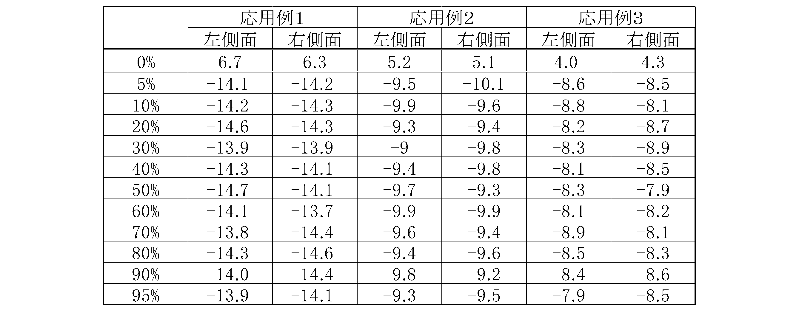
表5および図15Aを用いて、本発明の実施形態に係る貫通孔の第一面と第二面の開口径の関係性を説明する。表5は、実施例1の条件下でガラス基板10の厚さを100μmから200μmに変更した場合の貫通孔12の第一面101における開口部の径および第二面102における開口部の径を示す。図15Aは、表5をグラフにして示す図である。第一実施形態によれば、第二面102の開口径に関わらず、第二面102の開口径と第一面101の開口径の関係性は、第一面側開口径Φ1/第二面側開口径Φ2≧0.4以上となる。


また、図15Cは、本開示において形成される貫通孔および貫通電極の特徴を説明する図である。図15Cは、例えば、図29の領域Raを拡大して示す図である。図15Cに示されるように、貫通孔12(または貫通電極11)の直上に、導通電極31を形成することができる。これは、貫通孔12が所謂、有底形状であるためである。有底形状にすることで、貫通孔12上に直接に導通電極31を形成することが可能となる。このため、電極全体としての伝送距離が短縮され、伝送特性の向上および貫通孔12の微細化が可能となる。
また、実施形態において説明したように、本開示における貫通孔12の側面には側面形状が変化する変曲点がなく、表面が滑らかである。したがって、貫通孔12にめっき処理を行う場合、均一な金属膜等を形成することができるため、貫通孔12側面において寄生容量の発生を抑制することができる。貫通孔12の形状は、変曲点を有する形状や、ガラス基板の第一面から第二面まで径がほとんど変化しない所謂ストレート形状とすることも可能であるが、伝送特性の観点からは、寄生容量の発生を抑制することができる本開示に示す形状が望ましい。
次に、貫通孔12の側面形状について説明する。図16Aから図16Dは、各実施例および比較例に関し貫通孔の側面を説明する図である。図16Aは、第一実施形態における各実施例および各比較例の貫通孔の典型的な断面形状のSEM画像を示す図である。
図16Aにおいては、第一実施形態にかかるガラス基板の断面形状を観察しやすくするため、貫通孔12を樹脂材料を充填させている。第一面101から第二面102に向かうにつれて、側面の傾斜角度が変化する様子が分かる。
SEM画像において、コントラストが高く白色に見える箇所は、試料表面の傾斜面の角度が切り替わり、傾斜面の稜線となっている領域である。このため、白線で見える箇所は、試料表面の粗さのピークまたはボトムを示す箇所であり、これらの貫通孔の側面に形成されている稜線の存在状況や配置の程度によって、貫通電極の伝送特性に影響を与える貫通孔の側面の粗さを把握することができる。
ここで、図16Cを参照して、貫通孔の断面の稜線について説明する。図16Cは、第一実施形態における各実施例の貫通孔の稜線を説明する図である。図16C(a)は図16Bの実施例3を拡大して示す図である。また、図16C(b)は、SEM画像において観察される貫通孔について、側面および断面の稜線を実線で示す図である。
図16C(b)に示される例では、略平行な稜線のうち、稜線の間隔がもっとも広くなる場合は、稜線Rl1と稜線Rl2の間である。図16C(b)に示される例では、第一面101と垂直な方向の側面上の稜線の間隔はRs以下である。図16C(a)に示されるように、実施例3においては、稜線の間隔は、15.5μm以下である。
同様の手法で、稜線の状況を確認すると、実施例1においては、第一面101と垂直な方向における稜線と稜線の間隔は、2μm以上3μm以下の範囲である。また、実施例2においては、ガラス基板10の第一面101と垂直な方向における稜線と稜線の間隔は、5μm以上6μm以下の範囲である。
ここに示されるように、矢印で差し示されて破線で囲まれた箇所は、端部が立つ形状を有している。言い換えると、貫通孔12の側面とガラス基板10の第二面102との間には、ゆるやかに変化する箇所がなく、断面視において角度が一変している。つまり、貫通孔12の側面とガラス基板10の第二面102とは、端部が立つ形状を有しており、1000倍のSEM画像において、側面と第二面の領域とが明確に識別できる形状となっている。
続いて、図17を用いて、本発明の第一実施形態での各実施例、各比較例の貫通電極の伝送特性について説明する。図17は、第一実施形態における実施例1の貫通電極の伝送特性と、比較例1の貫通電極の伝送特性を示す図である。図17では貫通電極における伝送特性として伝送損失S21を測定した結果を示す。なお、実施例1から3は伝送特性が同じ傾向を示したため、代表して実施例1を示している。また、比較例1から3についても伝送特性がほとんど同じ傾向を示したので、代表して比較例1を示している。電極を形成するためのシード層の形成およびめっき処理等の形成条件は、実施例および比較例のいずれも共通とした。図17に示されるように、いずれの周波数領域においても、実施例の伝送損失のほうが比較例の伝送損失よりも小さいことが示される。したがって、貫通孔の側面については、分散粗さ、凹凸巾の値が小さいほど、貫通孔に形成される貫通電極における損失が小さくなり、伝送特性が良いことが分かる。
また、各実施例および各比較例について、ガラス基板10の厚みを変更させた場合の伝送特性S21についても測定した。この結果を表6に示す。表7に示されるように、ガラス基板10の厚みを100μm、150μm、200μmに設定したうえで、各実施例および各比較例に基づく条件で貫通孔及び貫通電極を作成し、の伝送特性を計測した。表7に示されるように、第一実施形態における各実施例では、各比較例に比べ伝送特性S21が良好な値を示していることが確認される。
なお、伝送特性の観点から、実施例1から3に示される貫通電極が比較例1から3に示される貫通電極よりも良好な結果が得られている。実施例の中で比較すると、実施例1が最も好ましく、実施例2、実施例3の順に良好であるということができる。

・設定条件:下限温度-40℃/30分、上限温度150℃/30分とした。
・試験装置TSA-43EL(エスペック製)
・各サイクル数で貫通電極を含む配線経路を抵抗の上昇を測定。
・NG基準:サイクル後の抵抗値が初期状態の抵抗値の10倍を超える場合にNGと判定

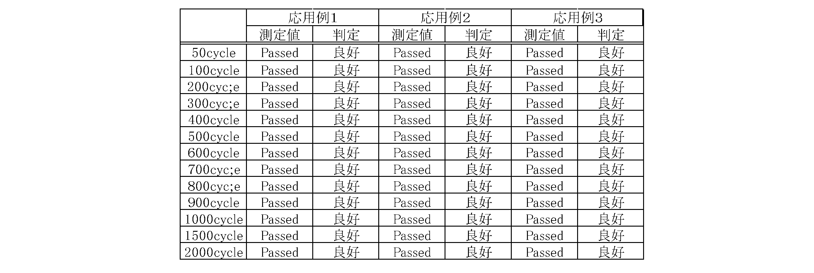
図18は、第一実施形態における多層配線基板1の構成の一例を示す図である。また、図19は、第一実施形態における多層配線基板1の構成の他の例を示す図である。多層配線基板1は、ガラス基板10、第一配線層21、および第二配線層22を含む。ガラス基板10の第一面101側には第一配線層21、ガラス基板10の第二面102側には第二配線層22が配置されている。ガラス基板10は、第一面101側から第二面102側まで貫通する貫通孔12を備える。貫通電極11は、貫通孔12の側面に沿って形成された導電体によって構成される。貫通電極11は第一配線層21の一部と第二配線層22の一部とを電気的に接続する。第一配線層21および第二配線層22は絶縁樹脂層25を含む。第一配線層21および第二配線層22は複数の層が積層された構成でもよく、その層数は必要に応じて設定してよい。貫通電極11は、第一配線層21と第二配線層22の間に電気的な接続を確立するための電極である。導通電極31は、多層配線基板1において基板の厚さ方向に導通を確保するための電極である。また、半導体素子用接合パッド50は、多層配線基板1に搭載する半導体回路を接続するための部材である。基板用接合パッド54は、多層配線基板1と他の基板とを接合するための部材である。
なお、貫通電極は、ガラス基板10の第一面101側から第二面102側を電気的に接続が可能であれば、図18に示すように貫通孔12の側面のみに導電体を配置してもよいし、図19に示すように貫通孔12に導電体を埋め込んでも構わない。
第一実施形態では、第一配線層21の貫通電極11のZ軸方向上に導通電極31を配置することが可能となる。
多層配線基板1の製造方法について、図3から図12を用いて説明する。まず、ガラス基板10に貫通孔12を形成する工程について説明する。
図20は、ガラス基板10を第一支持体62に張り合わせる工程を示す図である。
ガラス基板10の厚みは、エッチング後の厚みを考慮したうえで、用途に応じて適宜設定することができる。
ガラス基板10に第一支持体を貼り合わせるためには、例えば、ラミネーター、真空加圧プレス、減圧貼り合わせ機等を使用することができる。
続いて、図21は、レーザ改質部を形成する工程を示す図である。ガラス基板10にレーザ加工を実施することによって、ガラス基板10にレーザ改質部65が形成される。レーザ改質部65は、ガラス基板10に対しΦ3μm以下の形状で加工されており、ガラス基板10の厚み方向に連続的に形成される。この時、レーザ改質部65の周辺には、5μm以上の微小なクラック(以下、「マイクロクラック」ともいう。)が発生していないことが望ましい。レーザ改質部65の周辺に5μm以上のマイクロクラックが発生すると、エッチング加工後の貫通孔12に側面で分散粗さが1000nm以上かつ凹凸巾が1500nm以上となり、平滑な側面の貫通孔12を得ることが困難となる。また、5μm以上のマイクロクラックが発生した場合、後述するように、エッチング後の貫通孔12の側面ではガラス基板10の第一面101にと垂直な方向において、間隔をおいて変化する粗さが発生する。
続いて、図22は、第一配線層21を形成する工程を示す図である。図22に示されるように、積層構造体63のガラス基板10上の第一面101に導電層と絶縁樹脂層からなる第一配線層21の形成を行う。ここでは、ガラス基板10上には耐フッ酸金属層を含むシード層を形成した後に、セミアディティブ(SAP)工法で第一面101に貫通電極接続部41(または貫通電極間の配線)を形成する。不要となったシード層を除去した後に、絶縁樹脂層25を形成する。
次に絶縁樹脂層25の形成について、絶縁樹脂層25は熱硬化性樹脂であり、その材料は、エポキシ系樹脂、ポリイミド系樹脂、ポリアミド系樹脂の少なくとも一つを含み、かつシリカSiO2フィラーを含む材料である。絶縁樹脂層25の材料は、必要に応じて適宜選択することができる。但し、感光性絶縁樹脂材料を用いる場合は、フォトリソグラフィ性を確保するためにシリカSiO2フィラーの充填が困難となるため、感光性絶縁樹脂材料も使用可能であるが、熱硬化性樹脂を用いる方がより好ましい。
次に図23は、第二支持体を接着する工程を示す図である。図23に示されるように、積層構造体63の第一配線層21上に第二接着層71を形成し、第二接着層71上に第二支持体70を配置し接着する。
第二支持体70については、例えばガラスを用いることができ、ガラス基板10と同一の材料であることが望ましい。ガラス基板10が無アルカリガラスである場合、第二支持体70も無アルカリガラスであることが望ましい。また第二支持体70の厚みについては、ガラス基板10の厚みに応じて、適宜設定することができる。ただし、搬送可能な厚みであることが望ましく、その範囲は、300μm以上1,500μm以下の範囲である。
次に、図24は、第一支持体を剥離する工程を示す図である。図24に示されるように、ガラス基板10と第一支持体62を第一接着層61において剥離する。
続いて、図25は、貫通孔12を形成する工程を示す図である。
レーザ改質部65が形成されたガラス基板10に対し、所定のエッチング液でエッチング処理を施すことで貫通孔12が形成される。また、同時に、ガラス基板10の第二面もエッチングされ、ガラス基板10の厚さが減少することとなる。エッチングはガラス基板10の第二面102側から行われる。
エッチング液は、フッ酸を0.2質量%以上20.0質量%以下の範囲とし、硝酸を4.0質量%以上25.0質量%以下の範囲とし、フッ酸および硝酸以外の無機酸を0.5質量%以上11.0質量%以下の範囲として含有するものが用いられる。フッ酸および硝酸以外の無機酸としては、例えば、塩酸、硫酸、リン酸、スルファミン酸等が挙げられ、ガラス基板10中に含まれるケイ素以外の成分の種類に応じて、少なくとも1つの無機酸を含有させる。望ましくは、塩酸および硫酸を含有させたエッチング液であり、ガラス基板10に対するエッチングレートとしては、0.1μm/分以上10μm/分以下の範囲になるように適宜調整される。ガラス基板10に対するエッチングレートは、望ましくは0.25μm/分以上4μm/分以下の範囲であり、より望ましくは0.25μm/分以上0.5μm/分以下の範囲である。エッチング温度としては、特に限定されず、適宜調整することができるが、例えば10℃以上30℃以下の範囲となる。
なお、噴流を使用した浸漬処理、スプレー処理によるエッチング加工では、使用する装置のサイズによって、加工条件が異なることから、貫通孔12の形状を確認し、加工条件を設定することが望ましい。また、噴流を使用した浸漬処理では、他の機構として、超音波等を合わせて使用しても構わない。
次に、図26を参照して、貫通電極11の形成工程について説明する。図26は、貫通電極11を形成する工程を示す図である。
続いて、図28を参照して、第二支持体70および第二接着層71の剥離工程について説明する。図28は、第二支持体70および第二接着層71を剥離する工程を示す図である。図28に示されるように、第一配線層21の上方に形成された第二接着層71および第二支持体70を、第一面101側の第一配線層21と第二接着層71の界面より剥離する。これによって、図28に示されるように、第一面101側に第一配線層21、第二面102側に第二配線層22が形成された状態のガラス基板10が得られる。
第二支持体70を第二配線層22から剥離するにあたっては、第二接着層71に使用した材料に応じて、UV光の照射、加熱処理、物理剥離等から使用材料に応じた剥離方式を適宜選択することができる。また、第一配線層21と第二接着層71との接合面に、第二接着層71の残差が生じる場合、プラズマ洗浄、超音波洗浄、水洗、アルコールを使用した溶剤洗浄などを行ってもよい。
続いて、図29を参照して、ガラス基板10に形成される第一配線層21および第二配線層22の形成について説明する。図29は、第一配線層21および第二配線層22を形成する工程を示す図である。貫通電極11が形成されたガラス基板10に対し、第一面101に第一配線層21を形成し、第二面102に第二配線層22を形成する。第一配線層21および第二配線層22の形成工程において、最初に、感光性のレジストまたはドライフィルムレジストによってパターンを有するマスクを形成した後に、電解めっき処理によって配線を形成する。その後、物理密着処理、もしくは、化学的な密着処理を施した後に、絶縁樹脂層25を積層する。導通電極31については、レーザ加工等によって絶縁樹脂層25に孔を形成した後に、無電解めっき、もしくは、スパッタリングによる蒸着処理によって金属皮膜を形成する。上記金属皮膜にレジストを用いてパターンを有するマスクを形成し、電解めっきによって形成した孔に導電体を充填する。その後、マスクおよび余分の金属皮膜を除去する。上記工程は必要な層数に応じて複数回繰り返すことで、第一配線層21および第二配線層22が形成される。なお、第一配線層21および第二配線層22は多層配線基板1の反りを抑制するために、同じ層数であることが望ましい。第一配線層21および第二配線層22の層厚が異なる場合は、第一配線層21と第二配線層22に層数を変えても構わない。多層配線基板の用途に応じて、第一配線層21の層数および第二配線層22の層数は適宜設定してよい。
図30は、半導体素子100とBGA(Ball Grid Array:ボールグリッドアレイ)基板90のインターポーザ基板として、多層配線基板1を用いる場合を示す図である。図31は、図30の場合の断面を示す図である。また、図32は、通信用の電子デバイスに多層配線基板1および半導体素子100が用いられる場合を示す図である。図33は、図32の場合の断面を示す図である。電子デバイスとしては、層厚が800μm以下のものが用いられる。
上記電子デバイスは、貫通電極の伝送特性の影響によって、適応用途が限られており、本発明のガラス基板を用いた多層配線基板を使用することで電子デバイスの高周波数帯領域での適応が可能となる。
以上、本発明によれば、良好な伝送特性および高い信頼性を備えた貫通電極を形成することが可能なガラス基板およびそのようなガラス基板を備えた多層配線基板を得るが可能となる。
本開示は、次の態様も含む。
(態様1)
第一面と第二面を有し、前記第一面から前記第二面まで貫通する少なくとも1つの貫通孔を備えるガラス基板であって、
前記貫通孔の側面は、
前記第一面から距離0%以上10%未満の範囲において、側面の角度は4°以上7°以下の範囲となり、断面視において、前記貫通孔の側面を左側面および右側面とした場合、左側面の傾斜角度と右側面の傾斜角度の差が1.0°以下であり、
前記第一面から距離10%以上100%以下の範囲において、側面の角度は-7°以上-15°以下の範囲となり、左側面の傾斜角度と右側面の傾斜角度の差が1.0°以下となる、
ガラス基板。
(態様2)
態様1に記載のガラス基板であって、
前記貫通孔の側面は、前記第一面からの距離1%から距離5%以下の範囲に傾斜角度が変化する変曲点を有する、ガラス基板。
(態様3)
態様1または2に記載のガラス基板であって、
前記貫通孔では、第二面側の開口径Φ2と、第一面側の開口径Φ1の関係が、Φ1/Φ2≧0.4以上となる、ガラス基板。
(態様4)
請求項1から3のいずれか1つに記載のガラス基板であって、
前記ガラス基板の厚さ方向における前記貫通孔の裁断面における側面形状の
分散粗さが1,000nm以下かつ凹凸巾が1,500nm以下である、ことを特徴とするガラス基板。
(態様5)
態様1から4のいずれか1つに記載のガラス基板であって、
前記分散粗さは、前記側面の輪郭データに基づいて粗さ曲線を抽出し、前記粗さ曲線に設定区間を設定し、前記設定区間において式1によって算出された算術平均粗さであり、
前記凹凸巾は、前記設定区間において、最も高い部分と最も低い部の間の差である、ガラス基板。

態様1から5のいずれか1つに記載のガラス基板であって、
前記ガラス基板のSiO2比率は55質量%以上81質量%以下の範囲となる、ガラス基板。
(態様7)
態様1から6のいずれか1つ記載のガラス基板を含む多層配線基板であって、
前記多層配線基板に搭載される電子デバイスの層厚は800μm以下であり、
前記多層配線基板の厚みは100μm以上かつ400μm以下となる、ことを特徴とする多層配線基板。
(態様8)
態様1から7のいずれか1に記載のガラス基板の製造方法であって、
ガラス基板に対して、貫通孔形成予定部にレーザを照射する第1の工程、
レーザ照射された前記ガラス基板をエッチングし、貫通孔を形成する第2の工程
を有するガラス基板の製造方法。
(態様9)
態様8に記載のガラス基板の製造方法であって、
前記第2の工程は、レーザ照射された前記ガラス基板をエッチング液中に浸漬し、前記エッチング液において噴流の方向を切り替えるエッチング処理を行い、貫通孔を形成する工程である、ガラス基板の製造方法。
(態様10)
態様8または9に記載のガラス基板の製造方法であって、
前記第2の工程は、レーザ照射された前記ガラス基板にエッチング液を噴射し、前記ガラス基板または前記エッチング液の噴射口のいずれかを揺動させるエッチング処理を行い、貫通孔を形成する工程である、ガラス基板の製造方法。
(態様11)
態様8から10のいずれか1つに記載のガラス基板の製造方法であって、
前記第1の工程において、照射されるレーザは、レーザ発振波長が1064nm、532nm、または355nmのうちのいずれかの波長でありかつパルス幅が25ピコ秒以下である、ガラス基板の製造方法。
(態様12)
態様8から11のいずれか1つに記載のガラス基板の製造方法であって、
前記第1の工程において、前記レーザ照射周辺部に発生するマイクロクラックの最大長さが5μmである、ガラス基板の製造方法。
(態様13)
態様8から12のいずれか1つに記載のガラス基板の製造方法であって、
前記第2の工程において、フッ酸を0.2質量%以上20.0質量%以下の範囲とし、硝酸を4.0質量%以上25.0質量%以下の範囲とし、フッ酸および硝酸以外の無機酸を0.5質量%以上11.0質量%以下の範囲として含有するエッチング液が用いられる、ガラス基板の製造方法。
Claims (13)
- 第一面と第二面を有し、前記第一面から前記第二面まで貫通する少なくとも1つの貫通孔を備えるガラス基板であって、
前記貫通孔の側面は、
前記第一面から距離0%以上10%未満の範囲において、側面の角度は4°以上7°以下の範囲となり、断面視において、前記貫通孔の側面を左側面および右側面とした場合、左側面の傾斜角度と右側面の傾斜角度の差が1.0°以下であり、
前記第一面から距離10%以上100%以下の範囲において、側面の角度は-7°以上-15°以下の範囲となり、左側面の傾斜角度と右側面の傾斜角度の差が1.0°以下となる、
ガラス基板。 - 請求項1に記載のガラス基板であって、
前記貫通孔の側面は、前記第一面からの距離1%から距離5%以下の範囲に傾斜角度が変化する変曲点を有する、ガラス基板。 - 請求項1に記載のガラス基板であって、
前記貫通孔では、第二面側の開口径Φ2と、第一面側の開口径Φ1の関係が、Φ1/Φ2≧0.4以上となる、ガラス基板。 - 請求項1に記載のガラス基板であって、
前記ガラス基板の厚さ方向における前記貫通孔の裁断面における側面形状の
分散粗さが1,000nm以下かつ凹凸巾が1,500nm以下である、ことを特徴とするガラス基板。 - 請求項4に記載のガラス基板であって、
前記分散粗さは、前記側面の輪郭データに基づいて粗さ曲線を抽出し、前記粗さ曲線に設定区間を設定し、前記設定区間において式1によって算出された算術平均粗さであり、
前記凹凸巾は、前記設定区間において、最も高い部分と最も低い部の間の差である、ガラス基板。

- 請求項1から3のいずれか1項に記載のガラス基板であって、
前記ガラス基板のSiO2比率は55質量%以上81質量%以下の範囲となる、ガラス基板。 - 請求項1から3のいずれか1項に記載のガラス基板を含む多層配線基板であって、
前記多層配線基板に搭載される電子デバイスの層厚は800μm以下であり、
前記多層配線基板の厚みは100μm以上かつ400μm以下となる、ことを特徴とする多層配線基板。 - 請求項1に記載のガラス基板の製造方法であって、
ガラス基板に対して、貫通孔形成予定部にレーザを照射する第1の工程、
レーザ照射された前記ガラス基板をエッチングし、貫通孔を形成する第2の工程
を有するガラス基板の製造方法。 - 請求項8に記載のガラス基板の製造方法であって、
前記第2の工程は、レーザ照射された前記ガラス基板をエッチング液中に浸漬し、前記エッチング液において噴流の方向を切り替えるエッチング処理を行い、貫通孔を形成する工程である、ガラス基板の製造方法。 - 請求項8に記載のガラス基板の製造方法であって、
前記第2の工程は、レーザ照射された前記ガラス基板にエッチング液を噴射し、前記ガラス基板または前記エッチング液の噴射口のいずれかを揺動させるエッチング処理を行い、貫通孔を形成する工程である、ガラス基板の製造方法。 - 請求項8に記載のガラス基板の製造方法であって、
前記第1の工程において、照射されるレーザは、レーザ発振波長が1064nm、532nm、または355nmのうちのいずれかの波長でありかつパルス幅が25ピコ秒以下である、ガラス基板の製造方法。 - 請求項8に記載のガラス基板の製造方法であって、
前記第1の工程において、前記レーザ照射周辺部に発生するマイクロクラックの最大長さが5μmである、ガラス基板の製造方法。 - 請求項8に記載のガラス基板の製造方法であって、
前記第2の工程において、フッ酸を0.2質量%以上20.0質量%以下の範囲とし、硝酸を4.0質量%以上25.0質量%以下の範囲とし、フッ酸および硝酸以外の無機酸を0.5質量%以上11.0質量%以下の範囲として含有するエッチング液が用いられる、ガラス基板の製造方法。
Priority Applications (1)
| Application Number | Priority Date | Filing Date | Title |
|---|---|---|---|
| US19/094,104 US20250227842A1 (en) | 2022-09-30 | 2025-03-28 | Glass substrate, multilayer wiring substrate, and method for producing glass substrate |
Applications Claiming Priority (2)
| Application Number | Priority Date | Filing Date | Title |
|---|---|---|---|
| JP2022-158002 | 2022-09-30 | ||
| JP2022158002A JP7521565B2 (ja) | 2022-09-30 | 2022-09-30 | ガラス基板、多層配線基板、およびガラス基板の製造方法 |
Related Child Applications (1)
| Application Number | Title | Priority Date | Filing Date |
|---|---|---|---|
| US19/094,104 Continuation US20250227842A1 (en) | 2022-09-30 | 2025-03-28 | Glass substrate, multilayer wiring substrate, and method for producing glass substrate |
Publications (1)
| Publication Number | Publication Date |
|---|---|
| WO2024070321A1 true WO2024070321A1 (ja) | 2024-04-04 |
Family
ID=90477033
Family Applications (1)
| Application Number | Title | Priority Date | Filing Date |
|---|---|---|---|
| PCT/JP2023/029924 Ceased WO2024070321A1 (ja) | 2022-09-30 | 2023-08-21 | ガラス基板、多層配線基板、およびガラス基板の製造方法 |
Country Status (3)
| Country | Link |
|---|---|
| US (1) | US20250227842A1 (ja) |
| JP (3) | JP7521565B2 (ja) |
| WO (1) | WO2024070321A1 (ja) |
Citations (2)
| Publication number | Priority date | Publication date | Assignee | Title |
|---|---|---|---|---|
| JP2015146410A (ja) * | 2014-02-04 | 2015-08-13 | 大日本印刷株式会社 | ガラスインターポーザー基板、ガラスインターポーザー基板の製造方法 |
| JP2020521335A (ja) * | 2017-05-25 | 2020-07-16 | コーニング インコーポレイテッド | ジオメトリ属性を備えたビアを有する物品及びその製作方法 |
Family Cites Families (13)
| Publication number | Priority date | Publication date | Assignee | Title |
|---|---|---|---|---|
| JP4012936B2 (ja) * | 2004-08-06 | 2007-11-28 | 株式会社アライドマテリアル | 集合基板 |
| JP2007145656A (ja) * | 2005-11-29 | 2007-06-14 | Nippon Electric Glass Co Ltd | 縦穴を有するガラス基板およびその製造方法 |
| JP2011063456A (ja) * | 2009-09-15 | 2011-03-31 | Asahi Glass Co Ltd | 穿孔を有するガラス板およびガラス板の穿設方法 |
| JP2013080904A (ja) * | 2011-09-22 | 2013-05-02 | Hoya Corp | 基板製造方法、配線基板の製造方法、ガラス基板および配線基板 |
| JP2014139963A (ja) * | 2013-01-21 | 2014-07-31 | Ngk Spark Plug Co Ltd | ガラス基板の製造方法 |
| US20150329420A1 (en) * | 2014-05-19 | 2015-11-19 | Asahi Glass Company, Limited | Method for forming via hole in glass substrate by laser irradiation |
| JP2016072433A (ja) * | 2014-09-30 | 2016-05-09 | 大日本印刷株式会社 | 貫通電極基板及びその製造方法 |
| WO2018092480A1 (ja) * | 2016-11-17 | 2018-05-24 | 大日本印刷株式会社 | 貫通電極基板、貫通電極基板を用いた半導体装置、および貫通電極基板の製造方法 |
| US11478880B2 (en) * | 2017-03-06 | 2022-10-25 | Lpkf Laser & Electronics Ag | Method for producing at least one recess in a material by means of electromagnetic radiation and subsequent etching process |
| JP2018199605A (ja) * | 2017-05-29 | 2018-12-20 | Agc株式会社 | ガラス基板の製造方法およびガラス基板 |
| DE102019111634A1 (de) * | 2019-05-06 | 2020-11-12 | Lpkf Laser & Electronics Ag | Verfahren zur Herstellung von Mikrostrukturen in einem Glassubstrat |
| CN114556555A (zh) * | 2019-09-13 | 2022-05-27 | 康宁公司 | 用于减少通孔形成对于电子装置形成的影响的系统和方法 |
| WO2022196019A1 (ja) * | 2021-03-15 | 2022-09-22 | 日本電気硝子株式会社 | ガラス基板、貫通孔形成用ガラス原板及びガラス基板の製造方法 |
-
2022
- 2022-09-30 JP JP2022158002A patent/JP7521565B2/ja active Active
-
2023
- 2023-08-21 WO PCT/JP2023/029924 patent/WO2024070321A1/ja not_active Ceased
-
2024
- 2024-07-05 JP JP2024108784A patent/JP2024133088A/ja active Pending
-
2025
- 2025-02-25 JP JP2025027469A patent/JP2025068131A/ja active Pending
- 2025-03-28 US US19/094,104 patent/US20250227842A1/en active Pending
Patent Citations (2)
| Publication number | Priority date | Publication date | Assignee | Title |
|---|---|---|---|---|
| JP2015146410A (ja) * | 2014-02-04 | 2015-08-13 | 大日本印刷株式会社 | ガラスインターポーザー基板、ガラスインターポーザー基板の製造方法 |
| JP2020521335A (ja) * | 2017-05-25 | 2020-07-16 | コーニング インコーポレイテッド | ジオメトリ属性を備えたビアを有する物品及びその製作方法 |
Also Published As
| Publication number | Publication date |
|---|---|
| JP2024133088A (ja) | 2024-10-01 |
| JP2024051702A (ja) | 2024-04-11 |
| JP7521565B2 (ja) | 2024-07-24 |
| JP2025068131A (ja) | 2025-04-24 |
| US20250227842A1 (en) | 2025-07-10 |
Similar Documents
| Publication | Publication Date | Title |
|---|---|---|
| JP2023080267A (ja) | ジオメトリ属性を備えたビアを有する物品及びその製作方法 | |
| WO2024070320A1 (ja) | ガラス基板、多層配線基板、およびガラス基板の製造方法 | |
| US20240431027A1 (en) | Glass substrate, through-electrode, multilayer wiring substrate, and glass substrate manufacturing method | |
| US20250212324A1 (en) | Wiring board | |
| WO2016039223A1 (ja) | 構造体及びその製造方法 | |
| CN119547574A (zh) | 玻璃芯层叠结构体以及玻璃芯层叠结构体的制造方法 | |
| JP7521565B2 (ja) | ガラス基板、多層配線基板、およびガラス基板の製造方法 | |
| JP2022092505A (ja) | 基板ユニット、基板ユニットの製造方法及び半導体装置の製造方法 | |
| US20250261305A1 (en) | Glass substrate, multilayer wiring substrate, and method for producing glass substrate | |
| WO2024070319A1 (ja) | ガラス基板、多層配線基板、およびガラス基板の製造方法 | |
| JP2024051679A (ja) | ガラス基板、多層配線基板、およびガラス基板の製造方法 | |
| TW202428091A (zh) | 配線基板及配線基板之製造方法 | |
| JP2024006905A (ja) | 多層配線基板、多層配線基板の製造方法、および母材基板 | |
| CN117222122A (zh) | 一种局部镀厚金的线路板的制作方法 | |
| JP2024083846A (ja) | 配線基板及び配線基板の製造方法 | |
| US20240357739A1 (en) | Wiring board and manufacturing method therefor | |
| JP7816416B2 (ja) | 配線基板および配線基板の製造方法 | |
| JP7845597B1 (ja) | 配線基板及び配線基板の製造方法 | |
| US20240421059A1 (en) | Wiring substrate and manufacturing method of wiring substrate | |
| WO2025142479A1 (ja) | 多層配線母材基板、多層配線基板および多層配線基板の製造方法 | |
| TW202535118A (zh) | 多層配線基板、多層配線基板的製造方法及多層配線母材基板 | |
| JP2024146315A (ja) | 配線基板および配線基板の製造方法 | |
| JP2024009740A (ja) | 多層配線基板およびその製造方法 | |
| JP2021022651A (ja) | 配線基板の製造方法、配線基板形成用基板、配線基板中間品、配線基板および素子付配線基板 |
Legal Events
| Date | Code | Title | Description |
|---|---|---|---|
| 121 | Ep: the epo has been informed by wipo that ep was designated in this application |
Ref document number: 23871563 Country of ref document: EP Kind code of ref document: A1 |
|
| NENP | Non-entry into the national phase |
Ref country code: DE |
|
| WWE | Wipo information: entry into national phase |
Ref document number: 11202502056U Country of ref document: SG |
|
| WWP | Wipo information: published in national office |
Ref document number: 11202502056U Country of ref document: SG |
|
| 122 | Ep: pct application non-entry in european phase |
Ref document number: 23871563 Country of ref document: EP Kind code of ref document: A1 |