WO2024070271A1 - 導電性組成物、その焼結体、積層構造体、電子部品及び半導体装置 - Google Patents
導電性組成物、その焼結体、積層構造体、電子部品及び半導体装置 Download PDFInfo
- Publication number
- WO2024070271A1 WO2024070271A1 PCT/JP2023/029218 JP2023029218W WO2024070271A1 WO 2024070271 A1 WO2024070271 A1 WO 2024070271A1 JP 2023029218 W JP2023029218 W JP 2023029218W WO 2024070271 A1 WO2024070271 A1 WO 2024070271A1
- Authority
- WO
- WIPO (PCT)
- Prior art keywords
- conductive composition
- silver nanoparticles
- composition according
- organic solvent
- conductive
- Prior art date
- Legal status (The legal status is an assumption and is not a legal conclusion. Google has not performed a legal analysis and makes no representation as to the accuracy of the status listed.)
- Ceased
Links
Classifications
-
- B—PERFORMING OPERATIONS; TRANSPORTING
- B22—CASTING; POWDER METALLURGY
- B22F—WORKING METALLIC POWDER; MANUFACTURE OF ARTICLES FROM METALLIC POWDER; MAKING METALLIC POWDER; APPARATUS OR DEVICES SPECIALLY ADAPTED FOR METALLIC POWDER
- B22F1/00—Metallic powder; Treatment of metallic powder, e.g. to facilitate working or to improve properties
-
- B—PERFORMING OPERATIONS; TRANSPORTING
- B22—CASTING; POWDER METALLURGY
- B22F—WORKING METALLIC POWDER; MANUFACTURE OF ARTICLES FROM METALLIC POWDER; MAKING METALLIC POWDER; APPARATUS OR DEVICES SPECIALLY ADAPTED FOR METALLIC POWDER
- B22F1/00—Metallic powder; Treatment of metallic powder, e.g. to facilitate working or to improve properties
- B22F1/05—Metallic powder characterised by the size or surface area of the particles
-
- B—PERFORMING OPERATIONS; TRANSPORTING
- B22—CASTING; POWDER METALLURGY
- B22F—WORKING METALLIC POWDER; MANUFACTURE OF ARTICLES FROM METALLIC POWDER; MAKING METALLIC POWDER; APPARATUS OR DEVICES SPECIALLY ADAPTED FOR METALLIC POWDER
- B22F1/00—Metallic powder; Treatment of metallic powder, e.g. to facilitate working or to improve properties
- B22F1/10—Metallic powder containing lubricating or binding agents; Metallic powder containing organic material
- B22F1/102—Metallic powder coated with organic material
-
- B—PERFORMING OPERATIONS; TRANSPORTING
- B22—CASTING; POWDER METALLURGY
- B22F—WORKING METALLIC POWDER; MANUFACTURE OF ARTICLES FROM METALLIC POWDER; MAKING METALLIC POWDER; APPARATUS OR DEVICES SPECIALLY ADAPTED FOR METALLIC POWDER
- B22F9/00—Making metallic powder or suspensions thereof
-
- C—CHEMISTRY; METALLURGY
- C08—ORGANIC MACROMOLECULAR COMPOUNDS; THEIR PREPARATION OR CHEMICAL WORKING-UP; COMPOSITIONS BASED THEREON
- C08K—Use of inorganic or non-macromolecular organic substances as compounding ingredients
- C08K9/00—Use of pretreated ingredients
- C08K9/04—Ingredients treated with organic substances
-
- C—CHEMISTRY; METALLURGY
- C08—ORGANIC MACROMOLECULAR COMPOUNDS; THEIR PREPARATION OR CHEMICAL WORKING-UP; COMPOSITIONS BASED THEREON
- C08L—COMPOSITIONS OF MACROMOLECULAR COMPOUNDS
- C08L101/00—Compositions of unspecified macromolecular compounds
-
- H—ELECTRICITY
- H01—ELECTRIC ELEMENTS
- H01B—CABLES; CONDUCTORS; INSULATORS; SELECTION OF MATERIALS FOR THEIR CONDUCTIVE, INSULATING OR DIELECTRIC PROPERTIES
- H01B1/00—Conductors or conductive bodies characterised by the conductive materials; Selection of materials as conductors
-
- H—ELECTRICITY
- H01—ELECTRIC ELEMENTS
- H01B—CABLES; CONDUCTORS; INSULATORS; SELECTION OF MATERIALS FOR THEIR CONDUCTIVE, INSULATING OR DIELECTRIC PROPERTIES
- H01B1/00—Conductors or conductive bodies characterised by the conductive materials; Selection of materials as conductors
- H01B1/20—Conductive material dispersed in non-conductive organic material
- H01B1/22—Conductive material dispersed in non-conductive organic material the conductive material comprising metals or alloys
-
- H—ELECTRICITY
- H01—ELECTRIC ELEMENTS
- H01B—CABLES; CONDUCTORS; INSULATORS; SELECTION OF MATERIALS FOR THEIR CONDUCTIVE, INSULATING OR DIELECTRIC PROPERTIES
- H01B5/00—Non-insulated conductors or conductive bodies characterised by their form
Definitions
- the present invention relates to a conductive composition, a sintered body thereof, a laminated structure, an electronic component, and a semiconductor device.
- Flexible electronic devices such as bendable displays and solar cells, are attracting attention as essential devices for such high-performance communication terminals and the IoT market.
- Flexible electronic devices refer to various electronic devices mounted on stretchable substrates such as plastic, metal foil, paper, and flexible glass. These devices can be bent, twisted, and stretched, and can be incorporated into a variety of consumer and industrial products.
- Such flexible electronic devices can be realized by starting with the fabrication of an electronic device on a substrate such as plastic, and then configuring the electronic device as a circuit. Because plastic has a low heat resistance, low-temperature processing at a temperature of, for example, less than 150°C is required to form the metal wiring necessary for circuit configuration. Furthermore, such metal wiring is required to have low resistance so as to provide good electrical properties even in thin films. Furthermore, such metal wiring is required to have flexibility to follow the bending and stretching of the substrate, and durability (bending resistance) to withstand repeated bending and stretching.
- Conductive pastes for forming thin metal films are available in two types: resin-curing and sintered.
- Resin-curing conductive pastes form a conductive film when the thermosetting resin in the conductive paste is hardened by heat treatment.
- This type has the advantage of a low processing temperature, but the conductive powders are only fixed in place by the thermosetting resin while in contact with each other, and some of the resin remains, so the resistivity of the conductive film is relatively high.
- sintered conductive pastes can achieve a conductive film with low resistance because the metal is sintered (fused), but high-temperature processing at least 200°C or higher is required to sinter the metal particles.
- Patent Document 1 discloses a conductive composition that can be used to form a conductive circuit on a printed circuit board, the conductive composition comprising (A) fine silver particles with a number-average primary particle size of 40 nm to 400 nm, (B) a solvent, and (C) thermoplastic resin particles having a maximum endothermic peak in a DSC chart obtained by measurement using a differential scanning calorimeter in the range of 80°C to 170°C.
- the conductive composition disclosed in Patent Document 1 is of the sintered type, and is heat-treated at 200°C to form a thin film.
- the conductive film of a resin-curing conductive paste that can be processed at low temperatures has a high resistivity
- a sintered conductive paste that provides a conductive film with low resistance requires high-temperature processing.
- conductive pastes that boast low-temperature sinterability have been developed, they still require heat treatment at 150 to 200°C.
- the objective of the present invention is to provide a conductive composition that can be sintered at low temperatures of less than 150°C and that forms a conductive film that has low resistance, good flexibility, and bending resistance.
- a first embodiment of the present invention is the following conductive composition.
- (1) (A) surface-modified silver nanoparticles whose surfaces are coated with a lower carboxylic acid; (B) a binder resin; and (C) an organic solvent;
- a conductive composition comprising: A conductive composition, in which the lower carboxylic acid of the surface-modified silver nanoparticles (A) present in the conductive composition starts to be released from the silver nanoparticles at 40°C to 130°C.
- a second embodiment of the present invention is (12) a sintered body of the conductive composition according to any one of (1) to (11) above.
- a third embodiment of the present invention is (13) a laminated structure having the sintered body described in (12) above on a substrate.
- a fourth embodiment of the present invention is (14) an electronic component or a semiconductor device having the sintered body according to (12) above.
- the first embodiment of the present invention it is possible to obtain a conductive composition that can be sintered at a low temperature and forms a conductive film that has low resistance and excellent flexibility and bending resistance.
- the second embodiment of the present invention it is possible to obtain a sintered body that has low resistance and excellent flexibility and bending resistance.
- the third embodiment of the present invention it is possible to obtain a laminated structure having a sintered body on a substrate that has low resistance and excellent flexibility and bending resistance.
- an electronic component or semiconductor device that includes a sintered body that has low resistance and excellent flexibility and bending resistance.
- FIG. 3 is a TG-MS measurement graph of the conductive composition of the present invention.
- FIG. 1 is a scanning electron microscope (SEM) photograph of a cross section of a conductive film formed by screen-printing the conductive composition of the present invention and a conventional conductive composition on a polycarbonate film and heating at 120° C. for 30 minutes.
- 1 is a photograph of a wiring pattern of a conductive composition used as a test piece.
- low temperature sintering of the conductive composition refers to the fusion of silver nanoparticles to form a continuous silver film at a temperature below 150°C, preferably at a temperature of 120°C.
- the term “low resistance” refers to a conductive film having a specific resistance value of 1.0 ⁇ 10 -5 ⁇ cm or less.
- excellent flexibility of a sintered body means that when the sintered body is formed on a substrate, the sintered body has a degree of flexibility that enables it to follow the elongation and bending of the substrate.
- excellent bending resistance” of the sintered body means that even when the sintered body is repeatedly bent (for example, 500 times), the sintered body does not break and the change in resistivity is small.
- the conductive composition according to the first embodiment of the present invention comprises: (A) surface-modified silver nanoparticles whose surfaces are coated with a lower carboxylic acid; (B) a binder resin; and (C) an organic solvent; The lower carboxylic acid of the surface-modified silver nanoparticles (A) present in the conductive composition starts to be released from the silver nanoparticles at 40° C. to 130° C. According to this embodiment, a conductive composition can be obtained which can be sintered at a low temperature and can form a conductive film having low resistance, good flexibility and bending resistance.
- the conductive composition of this embodiment contains (A) surface-modified silver nanoparticles whose surfaces are coated with a lower carboxylic acid (hereinafter also referred to as "(A) surface-modified silver nanoparticles” or “component (A)”).
- (A) Surface-modified silver nanoparticles whose surfaces are coated with a lower carboxylic acid can be made conductive by sintering.
- metal nanoparticles are extremely active, most of them have a protective layer made of an organic substance formed on the particle surface to ensure the independence of the particles and prevent the particles from agglomerating. Although such a protective layer contributes effectively to the preservation of the particles, high-temperature processing is required to decompose the protective layer and fuse the metal particles, and even if a conductive film could be formed by low-temperature processing, the desired low resistance could not be obtained.
- the surface of the silver nanoparticles is covered with a low-molecular-weight carboxylic acid, which acts as a protective layer.
- the lower carboxylic acid of the surface-modified silver nanoparticles (A) present in this conductive composition starts to desorb from the silver nanoparticles at 40 to 130°C.
- the desorption start temperature is preferably 50 to 120°C, and more preferably 50 to 110°C.
- the desorption start temperature of the organic protection layer containing the lower carboxylic acid from the silver nanoparticles can be measured by thermogravimetry-mass spectrometry (hereinafter referred to as TG-MS analysis).
- TG-MS analysis is a method in which gas generated from a sample by heating in a TG is introduced online into a mass spectrometer (MS) to obtain a mass spectrum.
- MS mass spectrometer
- the carboxylic acid is difficult to detect by GCMS analysis, so a methylation reaction pyrolysis method is used to add a methylation reagent (e.g., tetramethylammonium hydroxide (TMAH), trimethylsulfonium hydroxide (TMSH), trimethyl( ⁇ , ⁇ , ⁇ -trifluoro-m-tolyl)ammonium hydroxide (TMTFTH), tetramethylammonium acetate (TMAAc), etc.) to the sample to detect the methylated form of the carboxylic acid generated.
- TMAH tetramethylammonium hydroxide
- TMSH trimethylsulfonium hydroxide
- TMTFTH trimethyl( ⁇ , ⁇ , ⁇ -trifluoro-m-tolyl)ammonium hydroxide
- TMAAc tetramethylammonium acetate
- the lower carboxylic acid a carboxylic acid having 5 or less carbon atoms is preferred, and a carboxylic acid having 2 to 5 carbon atoms is more preferred.
- the lower carboxylic acid may be either a saturated carboxylic acid or an unsaturated carboxylic acid.
- the lower carboxylic acid may be either a monocarboxylic acid or a dicarboxylic acid, with monocarboxylic acids being preferred, and examples thereof include lower monocarboxylic acids and monoesters of lower dicarboxylic acids.
- the lower carboxylic acid may be a hydroxycarboxylic acid in which the hydrocarbon group is substituted with a hydroxyl group.
- lower carboxylic acids include formic acid, acetic acid, propionic acid, butyric acid (butanoic acid), isobutyric acid (2-methylpropionic acid), 2-hydroxyisobutyric acid, valeric acid (pentanoic acid), isovaleric acid (3-methylbutanoic acid), lactic acid, maleic acid, monomethyl maleate, fumaric acid, monomethyl fumarate, methylmalonic acid, dimethylmalonic acid, methylsuccinic acid, malic acid, D-1-methyl malate, tartaric acid, 2-methyltartaric acid, acrylic acid, and methacrylic acid, and among these, acetic acid, butyric acid, lactic acid, monomethyl maleate, and 2-hydroxyisobutyric acid are preferred.
- the lower carboxylic acids may be used alone or in combination of two or more.
- Lower carboxylic acids can be attached to the surface of silver nanoparticles by using them during the synthesis of silver nanoparticles.
- lower carboxylic acids can be attached to the surface of silver nanoparticles by adding them to a composition containing silver nanoparticles.
- the surface-modified silver nanoparticles may have an organic substance other than a lower carboxylic acid on the surface, as long as the effect of the present invention is not impaired.
- organic substances include medium carboxylic acids with 6 to 12 carbon atoms, higher carboxylic acids with 13 or more carbon atoms, and alkylamines.
- the conductive composition of the present embodiment may contain surface-modified silver nanoparticles other than component (A) within a range that does not impair the effects of the present invention.
- Examples of such surface-modified silver nanoparticles include surface-modified silver nanoparticles whose surfaces are coated with a medium carboxylic acid, a higher carboxylic acid, and/or an alkylamine.
- the conductive composition preferably contains 15 to 100 parts by mass, and more preferably 20 to 100 parts by mass, of the surface-modified silver nanoparticles (A) relative to 100 parts by mass of the total amount of silver nanoparticles in the conductive composition.
- the total content of the silver nanoparticles in the conductive composition is preferably 40 to 89.7 parts by mass, more preferably 55 to 89.6 parts by mass, and even more preferably 67 to 84.5 parts by mass, per 100 parts by mass of the conductive composition.
- the average particle size of the silver nanoparticles is preferably 20 to 600 nm, more preferably 50 to 550 nm, and even more preferably 80 to 500 nm.
- the average particle size of the silver nanoparticles within the above range, the amount of lower carboxylic acid attached to the surface can be made appropriate, and sintering (fusion) of the silver nanoparticles can be promoted.
- One type of silver nanoparticle having an average particle size within the above range may be used, or two or more types may be used in combination.
- the average particle size of the silver nanoparticles is the average value of the long side lengths of 30 or more particles contained in an image observed with a scanning electron microscope, or the average particle size measured by the flow method using a laser diffraction particle size distribution meter (Partica LA-950V2 manufactured by Horiba, Ltd.).
- the silver nanoparticles can be produced by a known method.
- Known production methods include, but are not limited to, those described in, for example, International Publication No. 2012/059974, JP 2015-40319 A, and International Publication No. 2017/169534.
- the silver nanoparticles can be produced, for example, as follows, but are not limited to this production method.
- the silver nanoparticle preparation composition contains a silver compound that is the raw material for silver nanoparticles, a lower carboxylic acid to be attached to the surface of the silver nanoparticles as necessary, and an optional organic solvent.
- Preferred silver compounds include silver nitrate and silver oxalate, with silver oxalate being particularly preferred.
- Any organic solvent that can disperse a silver compound may be used, and examples of the organic solvent that can be used include alcohol-based solvents, glycol ether-based solvents, ether-based solvents, ester-based solvents, amine-based solvents, and ketone-based solvents.
- the ratio of each component in the composition can be adjusted as appropriate.
- the content of the silver compound in the composition is preferably 20 to 70 parts by mass relative to the total amount of the composition.
- the content of the lower carboxylic acid is preferably 0.1 to 20% by mass, more preferably 0.1 to 15% by mass, relative to the total amount of the composition.
- the content of the organic solvent can be adjusted according to the viscosity of the composition.
- the components can be mixed using general-purpose devices such as a mechanical stirrer, a magnetic stirrer, a vortex mixer, a planetary mill, a ball mill, a three-roll mill, a line mixer, a planetary mixer, and a dissolver.
- a mechanical stirrer such as a mechanical stirrer, a magnetic stirrer, a vortex mixer, a planetary mill, a ball mill, a three-roll mill, a line mixer, a planetary mixer, and a dissolver.
- the composition for preparing silver nanoparticles is subjected to a reaction, usually by heating, in a reaction vessel, which causes a thermal decomposition reaction of the silver compound to produce silver nanoparticles.
- a reaction usually by heating
- the reaction by heating may be carried out by introducing the composition into a reaction vessel that has been heated in advance, or by introducing the composition into the reaction vessel and then heating it.
- the reaction temperature may be any temperature at which the thermal decomposition reaction of the silver compound proceeds and silver nanoparticles are produced, for example, 50 to 250°C.
- the reaction time can be appropriately selected according to the desired average particle size and the composition of the composition corresponding to that.
- the reaction time is, for example, 1 minute to 100 hours.
- the silver nanoparticles produced by the thermal decomposition reaction of the silver compound are obtained as a mixture containing unreacted raw materials, so it is preferable to purify the silver nanoparticles.
- Purification methods include solid-liquid separation methods and precipitation methods that utilize the difference in specific gravity between the silver nanoparticles and unreacted raw materials such as organic solvents.
- the mixture containing the silver nanoparticles may be diluted with a low-boiling point solvent such as acetone or methanol to adjust its viscosity. After purification, the mixture can be washed as necessary and separated by filtration, centrifugation, etc. to obtain the silver nanoparticles.
- the average particle size of the resulting silver nanoparticles can be adjusted by adjusting the composition of the silver nanoparticle manufacturing composition and the reaction conditions.
- the silver nanoparticles obtained as described above are usually provided in the form of a slurry in which the silver nanoparticles are dispersed in an organic solvent from the viewpoint of storage stability.
- the organic solvent of the slurry is not particularly limited as long as it can disperse the silver nanoparticles, but for example, it is preferably the (C) organic solvent blended in the conductive composition described below.
- the organic solvent of the slurry may be any one of the above, or two or more of them may be used in combination.
- the organic solvent in the slurry is treated as the (C) organic solvent of the conductive composition, and the amount of the organic solvent in the slurry is included in the amount of the (C) organic solvent in the conductive composition of this embodiment.
- the conductive composition of this embodiment contains (B) binder resin (hereinafter also referred to as "component (B)").
- the (B) binder resin imparts flexibility and bending resistance to the sintered body of the conductive composition.
- the (B) binder resin improves the wettability of the conductive composition to the substrate when forming a coating film, and improves the adhesion to the substrate and the surface smoothness of the coating film.
- the weight average molecular weight of the (B) binder resin is preferably 5,000 to 200,000, more preferably 10,000 to 195,000, and even more preferably 15,000 to 190,000.
- the weight average molecular weight (Mw) refers to the weight average molecular weight converted into polystyrene using a calibration curve of standard polystyrene by gel permeation chromatography (GPC).
- GPC gel permeation chromatography
- the binder resin may be a known binder resin, for example, cellulose-based resins such as ethyl cellulose, hydroxyethyl cellulose, ethylhydroxy cellulose, hydroxypropyl cellulose, methyl cellulose, cellulose acetate, and cellulose butyrate; vinyl-based resins such as polyvinyl alcohol, polyvinyl acetate, polyvinyl butyral, polyvinyl acetal, polyvinyl pyrrolidone, polyacrylamide, and polyvinyl chloride; styrene-based resins such as polystyrene, styrene-maleic anhydride copolymer, styrene-acrylic copolymer, and styrene-butadiene copolymer; polyolefin-based resins such as polyethylene, polypropylene, polybutadiene, and polyisoprene; polyurethane-based resins; polyester-based resins; polyurethan
- the binder resin may be any one of these, or two or more of these may be used in combination. From the viewpoint of further improving the surface smoothness of the coating film, the binder resin is preferably a cellulose-based resin, and more preferably ethyl cellulose.
- the content of the (B) binder resin in the conductive composition is preferably 0.3 to 10 parts by mass, more preferably 0.4 to 5 parts by mass, and even more preferably 0.5 to 3 parts by mass, per 100 parts by mass of the conductive composition, from the viewpoint of achieving both low resistance and flexibility and bending resistance.
- the mass ratio of the surface-modified silver nanoparticles (A) to the binder resin (B) is preferably 90:10 to 99.7:0.3, and more preferably 91:9 to 99.6:0.4.
- the conductive composition of the present embodiment contains (C) an organic solvent (hereinafter also referred to as “component (C)”).
- component (C) organic solvent disperses the (A) surface-modified silver nanoparticles and dissolves the (B) binder resin.
- the (C) organic solvent may be any organic solvent that, when combined with (A) surface-modified silver nanoparticles whose surfaces are coated with a lower carboxylic acid, can cause the lower carboxylic acid of the (A) surface-modified silver nanoparticles present in the conductive composition to begin to desorb from the silver nanoparticles at 40°C to 130°C.
- the (C) organic solvent preferably contains an organic solvent having a boiling point of 180°C to 270°C, and more preferably contains an organic solvent having a boiling point of 200°C to 240°C.
- the organic solvent remains appropriately until the lower carboxylic acids of the (A) surface-modified silver nanoparticles begin to desorb, promoting the desorption of the lower carboxylic acids.
- the conductive composition has good workability.
- the desorption of the lower carboxylic acids is promoted and the organic solvent can be sufficiently removed in the low-temperature heating process.
- the organic solvent (C) preferably contains a polar organic solvent, and more preferably contains a polar organic solvent having a boiling point of 180°C to 270°C.
- Examples of polar solvents having a boiling point of 180°C to 270°C include glycol ether-based solvents such as diethylene glycol monomethyl ether, diethylene glycol diethyl ether, diethylene glycol monobutyl ether (common name: butyl carbitol), diethylene glycol dibutyl ether, diethylene glycol butyl methyl ether, diethylene glycol monobutyl ether acetate, dipropylene glycol monomethyl ether, triethylene glycol monomethyl ether, triethylene glycol butyl methyl ether, triethylene glycol dimethyl ether, tripropylene glycol dimethyl ether, and ethylene glycol monophenyl ether; or terpineol-based solvents such as terpineol and dihydroterpineol.
- glycol ether-based solvents such as diethylene glycol monomethyl ether, diethylene glycol diethyl ether, diethylene glycol monobutyl ether (common name: butyl
- the organic solvent (C) may be used alone or in combination of two or more.
- glycol ether-based solvents having a boiling point of 180°C to 270°C have a polarity close to that of lower carboxylic acids, and therefore can further promote the elimination of lower carboxylic acids from the surface-modified silver nanoparticles (A).
- the organic solvent (C) preferably contains a glycol ether-based solvent having a boiling point of 180°C to 270°C.
- diethylene glycol monobutyl ether common name: butyl carbitol is more preferable.
- the content of the glycol ether-based solvent having a boiling point of 180°C to 270°C in the organic solvent (C) is preferably 20 to 100 parts by mass, more preferably 30 to 100 parts by mass, and even more preferably 40 to 100 parts by mass, relative to 100 parts by mass of the organic solvent (C).
- the conductive composition of this embodiment may contain an organic solvent having a boiling point of less than 180°C, an organic solvent having a boiling point of more than 270°C, or a non-polar organic solvent, as long as the lower carboxylic acid of the surface-modified silver nanoparticles (A) present in the conductive composition can begin to be released from the silver nanoparticles at 40°C to 130°C.
- the content of (C) the organic solvent is not particularly limited, but from the viewpoint of viscosity adjustment and coating film formability, it is preferably 10 to 50 parts by mass, more preferably 10 to 40 parts by mass, and even more preferably 15 to 30 parts by mass, per 100 parts by mass of the conductive composition.
- the conductive composition of this embodiment may contain additives such as inorganic pigments, organic pigments, coupling agents such as silane coupling agents, leveling agents, thixotropic agents, insulating particles, interface treatment agents, dyes, plasticizers, defoamers, foam breakers, and antioxidants, as necessary, within the scope of the invention.
- additives such as inorganic pigments, organic pigments, coupling agents such as silane coupling agents, leveling agents, thixotropic agents, insulating particles, interface treatment agents, dyes, plasticizers, defoamers, foam breakers, and antioxidants, as necessary, within the scope of the invention.
- the method for producing the conductive composition of this embodiment is not particularly limited, and can be produced, for example, by blending components (A) to (C) and, if necessary, additives in a predetermined ratio and stirring and mixing.
- a stirring and mixing means known devices can be used, such as a Henschel mixer, planetary mixer, dissolver, bead mill, Raikai machine, pot mill, roll mill, triple roll mill, rotary mixer, twin-shaft mixer, etc.
- Components (A) to (C) and any additives can be mixed simultaneously, or some of them can be mixed first and the rest can be mixed later.
- the method of applying the conductive composition of this embodiment is not particularly limited, and for example, the conductive composition can be applied to a desired portion of a substrate or the like by a known printing method, dispensing method, or coating method.
- Printing methods include, but are not limited to, screen printing, lithographic printing, carton printing, metal printing, offset printing, gravure printing, flexographic printing, inkjet printing, and the like.
- Dispensing methods include, but are not limited to, jet dispensers, air dispensers, and the like.
- Coating methods include, but are not limited to, dip coating, spray coating, bar coater coating, gravure coating, reverse gravure coating, spin coater coating, and the like.
- the conductive composition of this embodiment is a sintered conductive composition, and by heating and baking at a predetermined temperature, the lower carboxylic acid of the surface-modified silver nanoparticles (A) is eliminated, and the silver nanoparticles are fused together to form a conductive film that is a sintered body.
- the heating temperature can be 100°C to 300°C, but when used in the manufacture of flexible electronic devices, the heating temperature is preferably less than 150°C, for example, 100°C or more and less than 150°C, more preferably 100 to 140°C, even more preferably 110 to 130°C, and particularly preferably 120°C, from the viewpoint of not damaging the substrate such as plastic.
- the heating time may vary depending on the heating temperature, but is preferably 0.25 to 4 hours, more preferably 0.5 to 2 hours.
- the conductive composition of this embodiment can obtain a sintered body with low resistance even by heat treatment at a low temperature of less than 150°C.
- the conductive composition of this embodiment can form a sintered film with a resistivity of 1.0 x 10⁻⁵ ⁇ cm or less under heating conditions of 120°C for 30 minutes. This is because the silver nanoparticles are fused to form a continuous silver film even by heat treatment at a low temperature of less than 150°C, and a large number of conductive paths are formed (see the right photo in Figure 2).
- the silver nanoparticles cannot be fused by low-temperature heat treatment, and the conductive paths are few and only the contact points of the silver nanoparticles (see the left photo in Figure 2), so it was not possible to achieve a resistivity value of 1.0 x 10⁻⁵ ⁇ cm or less.
- the method for measuring the resistivity is not particularly limited, but for example, the method described in [Measurement of resistivity after heating at 120°C for 30 minutes] in the examples described later is followed.
- a specific example of the method for measuring the resistivity is as follows.
- a polycarbonate resin film product name: Makrofol (registered trademark) DE 1-1 000000, manufactured by Covestro
- the size of the substrate is 100 mm x 148 mm, and the thickness is 250 ⁇ m.
- five types of wiring patterns (electrode length: 60 mm, electrode width: 0.2 mm, 0.5 mm, 1 mm, 2 mm, 3 mm) of the conductive composition as shown in FIG. 3 are printed by a screen printer.
- the screen mask used is SUS 500 mesh, emulsion thickness 5 ⁇ m, and calendared. After printing, the substrate is heated and dried at 120° C. for 30 minutes in a constant temperature dryer. The film thickness of the obtained cured product of the wiring pattern (hereinafter simply referred to as "wiring pattern”) is measured.
- the film thickness is measured, for example, using a surface roughness and shape measuring instrument (model number: Surfcom 1500SD-2) manufactured by Tokyo Seimitsu Co., Ltd.
- the resistance values at both ends of the cured wiring pattern are measured by a four-terminal method using a HIOKI resistance measuring device RM3545-02.
- the specific resistance value is calculated from the following formula (1).
- ⁇ is the resistivity
- R is the measured resistance value ( ⁇ ) at both ends of the wiring pattern
- A is the cross-sectional area (cm 2 ) of the wiring pattern
- L is the length (cm) of the wiring pattern.
- the conductive composition of this embodiment can form a sintered film having a resistivity change rate of 50% or less, more preferably 40% or less, and even more preferably 35% or less before and after 500 repeated bending.
- the bending method and the method for measuring the resistivity change rate are, for example, according to the method described in the "Resistivity change rate before and after bending test" in the Examples below.
- a specific example of the method for measuring the rate of change in resistivity before and after the bending test is as follows.
- a wiring pattern (electrode length: 60 mm, electrode width: 1 mm) is printed on a polycarbonate resin film using a screen printer, and the wiring pattern is dried by heating at 120°C for 30 minutes in a constant temperature dryer to prepare a test piece.
- ASTM D1327 JIS K-5600-5-1
- a bending test is performed up to 500 times using a 4 mm ⁇ rod so that the electrode printed surface is folded in a mountain shape.
- the resistivity of the test piece after the bending test is calculated, and the rate of change in resistivity (%) relative to the resistivity before the bending test is obtained.
- the resistivity is calculated from the above formula (1).
- the coating film has small surface irregularities and excellent surface smoothness
- the sintered film obtained by heat-treating the coating film also has high surface smoothness.
- the conductive composition of this embodiment can form a sintered film having a surface irregularity height difference of 6 ⁇ m or less, more preferably 5 ⁇ m or less, and even more preferably 3 ⁇ m or less, under heating conditions of 120° C. for 30 minutes.
- the surface irregularity height difference can be measured, for example, according to the method described in [Measurement of Coating Film Surface Smoothness] in the Examples below.
- a specific example of the coating surface smoothness measurement is as follows.
- a wiring pattern (electrode length: 60 mm, electrode width: 1 mm) is printed on a polycarbonate resin film using a screen printer, and the pattern is dried by heating at 120° C. for 30 minutes in a constant temperature dryer to prepare a test piece.
- a 2D cross-sectional profile and 3D images are obtained using a confocal microscope (LASERTEC CORPORATION, OPTELICS H1200) to confirm the unevenness height difference of the coating surface.
- the unevenness height difference is defined as the maximum width of the unevenness of the coating surface.
- the unevenness of the coating surface of the conductive composition can be adjusted, for example, by the structure, molecular weight, and amount of the binder resin (B) and the amount of the organic solvent (C).
- the fewer the polar groups in the binder resin the better the wettability to the organic substrate, and the smaller the unevenness of the coating surface tends to be.
- the thixotropy is reduced, the wettability to the organic substrate is improved, and the unevenness of the coating surface tends to be smaller.
- the conductive composition of this embodiment can be used to form conductive circuits on printed circuit boards, electrodes of capacitors, etc., and is particularly suitable for forming conductive circuits and electrodes on flexible substrates.
- the conductive composition of this embodiment can also be used to form electrodes and heating wires of printable devices such as printable heaters.
- the conductive composition of this embodiment can also be used to bond components of electronic components or semiconductor devices together, and substrates and components, etc.
- the sintered body according to the second embodiment of the present invention is a sintered body of the conductive composition according to the first embodiment.
- the sintered body according to the present embodiment has low resistance and excellent flexibility and bending resistance.
- the laminated structure according to the third embodiment of the present invention has the sintered body according to the second embodiment on a substrate.
- the laminated structure according to the present embodiment has a sintered body having low resistance and excellent flexibility and bending resistance on a substrate, and is therefore suitable for use in flexible electronic devices, but is not limited thereto.
- the substrate may be a flexible substrate such as a plastic film, or a hard substrate such as a metal, glass, or ceramic.
- the plastic film include, but are not limited to, a polyimide film, a PET film, a polycarbonate film, and the like.
- the electronic component or semiconductor device according to the fourth embodiment of the present invention has the sintered body according to the second embodiment described above. Since the sintered body has low resistance and excellent flexibility and bending resistance, it is useful as a flexible electronic device, but is not limited thereto.
- Flexible electronic devices include, but are not limited to, flexible touch panels, flexible lighting, flexible batteries, flexible printed circuit boards, flexible color filters, surface cover lenses for smartphones, printable heaters, flexible sensors, and flexible actuators.
- Examples 1 to 21, Comparative Examples 1 to 3 The components shown in Table 1 were stirred and mixed using a hybrid mixer according to the formulation shown in Table 1, and then uniformly dispersed using a three-roll mill to prepare conductive compositions of the examples and comparative examples. In Table 1, the amount of each component is expressed in parts by mass (unit: g). The components used in the examples and comparative examples are as follows.
- the following components (A) and (A') were produced in a manner similar to the above-mentioned method for producing silver nanoparticles.
- Various carboxylic acids or alkylamines (8.2 g), and butanol (37.5 g) or a mixture of butanol (8.75 g) and ethylene glycol (28.75 g) were added to a 50 mL glass centrifuge tube containing a magnetic stirrer, and the mixture was stirred for about 1 minute. Then, silver oxalate (25.0 g) was added and stirred for about 10 minutes to obtain a composition for preparing silver nanoparticles.
- A Surface-modified silver nanoparticles coated with a lower carboxylic acid
- A-1 Surface-modified silver nanoparticles coated with acetic acid (average particle size: 100 nm, carbon number: 2)
- A-2) Surface-modified silver nanoparticles 1 coated with lactic acid (average particle size: 100 nm, carbon number: 3)
- A-3) Surface-modified silver nanoparticles 2 coated with lactic acid (average particle size: 500 nm, carbon number: 3)
- A-4) Surface-modified silver nanoparticles coated with butyric acid (average particle size: 100 nm, carbon number: 4)
- A-5) Surface-modified silver nanoparticles coated with methyl maleate (average particle size: 100 nm, carbon number: 5)
- A' Surface-modified silver nanoparticles other than component
- A A'-1): Surface-modified silver nanoparticles coated with octylamine (average particle size: 100 nm, carbon number: 8)
- Binder Resin (B-1): Polyvinyl butyral resin 1 (product name: BX-L, manufactured by Sekisui Chemical Co., Ltd., weight average molecular weight: 18,000)
- B-2 Polyvinyl butyral resin 2 (product name: KS-5Z, manufactured by Sekisui Chemical Co., Ltd., weight average molecular weight: 130,000)
- B-3 Ethyl cellulose resin 1 (product name: N14, manufactured by ASHLAND, weight average molecular weight: 87,100)
- B-5 Ethyl cellulose resin 3 (product name: N200, manufactured by ASHLAND, weight average molecular weight: 187,800)
- C-1 Diethylene glycol diethyl ether (manufactured by Toho Chemical Industry Co., Ltd., boiling point: 189° C.)
- C-2 Dihydroterpineol (manufactured by Nippon Terpene Chemical Co., Ltd., boiling point: 207° C.)
- C-3 Terpineol (manufactured by Kobayashi Fragrance Co., Ltd., boiling point: 219° C.)
- C-4 Diethylene glycol monobutyl ether (common name: butyl carbitol) (manufactured by Taishin Chemical Co., Ltd., boiling point: 230° C.)
- C-5 Diethylene glycol dibutyl ether (manufactured by Toho Chemical Industry Co., Ltd., boiling point: 256° C.)
- C-6 Tetraethylene glycol dimethyl ether (manufactured by Taishin Chemical Co., Ltd.,
- TG-MS analysis was carried out to measure the detachment start temperature of the protective layer of the surface-modified silver nanoparticles.
- a methylating agent, tetramethylammonium hydroxide (TMAH) was added to each of the conductive compositions of the examples and comparative examples to prepare measurement samples, which were then measured using a TG-MS analyzer (NETZSCH STA 449F3, manufactured by NETZSCH) under the following measurement conditions: a measurement sample weight of 90 mg, a measurement temperature of 30°C to 320°C, and a helium atmosphere.
- the protective layer desorption start temperature was evaluated as ⁇ when it was 40°C to 80°C, ⁇ when it was 80°C to 130°C, and ⁇ when it exceeded 130°C. The results are shown in Table 1.
- a polycarbonate resin film product name: Makrofol (registered trademark) DE 1-1 000000, manufactured by Covestro
- the size of the substrate was 100 mm ⁇ 148 mm, and the thickness was 250 ⁇ m.
- five types of wiring patterns of the conductive composition as shown in FIG. 3 were printed by a screen printer.
- the screen mask used was SUS 500 mesh, emulsion thickness 5 ⁇ m, and calendared.
- the film thickness of the obtained cured product of the wiring pattern (hereinafter simply referred to as "wiring pattern") was 2 to 10 ⁇ m.
- the film thickness was measured using a surface roughness shape measuring instrument (model number: Surfcom 1500SD-2) manufactured by Tokyo Seimitsu Co., Ltd.
- the resistance values of both ends of the cured wiring pattern were measured by a four-terminal method using a HIOKI resistance measuring device RM3545-02. The specific resistance value was calculated from the following formula (1).
- ⁇ R ⁇ A/L Equation (1)
- ⁇ is the resistivity
- R is the measured resistance ( ⁇ ) at both ends of the wiring pattern
- A is the cross-sectional area (cm 2 ) of the wiring pattern
- L is the length (cm) of the wiring pattern.
- the conductive film obtained from the conductive composition of Comparative Example 1 which did not contain (A) surface-modified silver nanoparticles the surface of which was coated with a lower carboxylic acid, but contained (A'-1): surface-modified silver nanoparticles coated with octylamine, had a high specific resistance of 15 ⁇ 10 -5 ⁇ cm.
- the conductive composition of Comparative Example 2 in which the detachment starting temperature of the protective layer of the surface-modified silver nanoparticles exceeded 130° C., had a high specific resistance of 8 ⁇ 10 ⁇ 5 ⁇ cm.
- the present invention is a conductive composition that can be sintered at low temperatures and forms a conductive film with low resistance and excellent flexibility and bending resistance, and is particularly suitable for producing conductive circuits and electrodes on flexible substrates.
Landscapes
- Chemical & Material Sciences (AREA)
- Health & Medical Sciences (AREA)
- Chemical Kinetics & Catalysis (AREA)
- Medicinal Chemistry (AREA)
- Polymers & Plastics (AREA)
- Organic Chemistry (AREA)
- Physics & Mathematics (AREA)
- Dispersion Chemistry (AREA)
- Spectroscopy & Molecular Physics (AREA)
- Conductive Materials (AREA)
Abstract
Description
本発明の第一の実施形態は、以下の導電性組成物である。
(1)(A)表面が低級カルボン酸で被覆された表面修飾銀ナノ粒子と、
(B)バインダー樹脂と、
(C)有機溶剤と、
を含む導電性組成物であって、
導電性組成物中に存在する前記(A)表面修飾銀ナノ粒子の低級カルボン酸が、40℃~130℃で銀ナノ粒子から脱離開始する、導電性組成物。
(2)前記(A)表面修飾銀ナノ粒子の中の低級カルボン酸が、酢酸、酪酸、乳酸、マレイン酸メチル及びヒドロキシイソ酪酸より選ばれる少なくとも1種である、上記(1)に記載の導電性組成物。
(3)前記(C)有機溶剤が、180~270℃の沸点を有する有機溶剤を含む、上記(1)又は(2)に記載の導電性組成物。
(4)前記(A)表面修飾銀ナノ粒子の平均粒子径が、20nm~600nmである、上記(1)~(3)のいずれか1項に記載の導電性組成物。
(5)(B)バインダー樹脂の重量平均分子量が、5,000~200,000である、上記(1)~(4)のいずれか1項に記載の導電性組成物。
(6)前記(B)バインダー樹脂が、セルロース系樹脂である、上記(1)~(5)のいずれか1項に記載の導電性組成物。
(7)前記(A)表面修飾銀ナノ粒子と(B)バインダー樹脂との質量比(成分(A):成分(B))が、90:10~99.7:0.3である、上記(1)~(6)のいずれか1項に記載の導電性組成物。
(8)前記(C)有機溶剤の含有量が、導電性組成物100質量部に対して10質量部~50質量部である、上記(1)~(7)のいずれか1項に記載の導電性組成物。
(9)120℃30分の加熱条件において、比抵抗値が1.0×10⁻⁵Ω・cm以下である焼結膜を形成する、上記(1)~(8)のいずれか1項に記載の導電性組成物。
(10)折り曲げを500回繰り返す前後における比抵抗値変化率が50%以下である焼結膜を形成する、上記(1)~(9)のいずれか1項に記載の導電性組成物。
(11)120℃30分の加熱条件において、表面凹凸高低差が6μm以下である焼結膜を形成する、上記(1)~(10)のいずれか1項に記載の導電性組成物。
本発明の第三の実施形態は、(13)上記(12)に記載の焼結体を基材上に有する積層構造体である。
本発明の第四の実施形態は、(14)上記(12)に記載の焼結体を有する電子部品又は半導体装置である。
本明細書中において、「低抵抗」とは、導電膜が1.0×10⁻⁵Ω・cm以下の比抵抗値を有することを言う。
本明細書中において、焼結体の「優れた柔軟性」とは、基材上に焼結体が形成されている場合、焼結体が基材の伸びや曲げに追従できる程度の柔軟性を有することを言う。
本明細書中において、焼結体の「優れた曲げ耐性」とは、焼結体を繰り返し(例えば、500回)曲げた場合でも、焼結体の破断が起こらず、比抵抗値変化が小さいことを言う。
本発明の第一の実施形態である導電性組成物は、
(A)表面が低級カルボン酸で被覆された表面修飾銀ナノ粒子と、
(B)バインダー樹脂と、
(C)有機溶剤と、
を含み、この導電性組成物中に存在する前記(A)表面修飾銀ナノ粒子の低級カルボン酸は、40℃~130℃で銀ナノ粒子から脱離開始する。本実施形態によれば、低温焼結が可能であり、かつ低抵抗で、良好な柔軟性及び曲げ耐性を有する導電膜を形成する導電性組成物を得ることができる。
本実施形態の導電性組成物は、(A)表面が低級カルボン酸で被覆された表面修飾銀ナノ粒子(以下、「(A)表面修飾銀ナノ粒子」又は「成分(A)」とも言う)を含む。(A)表面が低級カルボン酸で被覆された表面修飾銀ナノ粒子は、焼結することにより導電性を付与することができる。
導電性組成物中の銀ナノ粒子全体の含有量は、導電性組成物100質量部に対して40~89.7質量部が好ましく、55~89.6質量部がより好ましく、67~84.5質量部がさらに好ましい。
本実施形態の導電性組成物は、(B)バインダー樹脂(以下、「成分(B)」とも言う)を含む。(B)バインダー樹脂は、導電性組成物の焼結体に、柔軟性及び耐曲げ性を付与する。また、(B)バインダー樹脂により、導電性組成物の塗膜を形成する際に基材への塗れ性が向上し、基材との密着性及び塗膜の表面平滑性が向上する。
本実施形態の導電性組成物は、(C)有機溶剤(以下、「成分(C)」とも言う)を含む。(C)有機溶剤は、(A)表面修飾銀ナノ粒子を分散し、(B)バインダー樹脂を溶解する。
比抵抗値の測定方法の具体例は、以下の通りである。有機基材として、ポリカーボネート樹脂のフィルム(品名:Makrofol(登録商標)DE 1-1 000000、コベストロ社製)を用いる。基材の大きさは100mm×148mmであり、厚さは250μmである。この基材の表面に、図3に示すような導電性組成物の配線パターン5種(電極長さ:60mm、電極幅:0.2mm、0.5mm、1mm、2mm、3mm)を、スクリーン印刷機にて印刷する。スクリーンマスクは、SUS 500メッシュ、乳剤厚5μm、カレンダー処理のものを用いる。印刷後、定温乾燥機で、120℃で30分間、加熱乾燥させる。得られた配線パターンの硬化物(以下では、単に「配線パターン」という。)の膜厚を測定する。膜厚は、例えば、株式会社東京精密製表面粗さ形状測定機(型番:サーフコム1500SD-2)を用いて測定する。硬化後の配線パターンの両端の抵抗値を、HIOKI製抵抗測定装置RM3545-02を用い、4端子法で測定する。比抵抗値を以下の式(1)から算出する。
ρ=R×A/L 式(1)
ここで、ρは比抵抗値、Rは配線パターンの両端の実測抵抗値(Ω)、Aは配線パターンの断面積(cm2)、Lは配線パターンの長さ(cm)である。
折曲げ試験前後における比抵抗値変化率の測定方法の具体例は、以下の通りである。ポリカーボネート樹脂のフィルム上に配線パターン(電極長さ:60mm、電極幅:1mm)を、スクリーン印刷機にて印刷し、定温乾燥機で120℃で30分間、加熱乾燥させたものを試験片とし、ASTM D1327 (JIS K-5600-5-1)に準拠して、4mmφのロッドを用いて、電極印刷面が山折りとなるように折り曲げ試験を500回まで実施する。折り曲げ試験後の試験片の比抵抗値を算出し、折り曲げ試験前の比抵抗値に対する比抵抗値変化率(%)を求める。比抵抗値は、上記式(1)から算出する。
塗膜表面平滑性測定の具体例は、以下の通りである。ポリカーボネート樹脂のフィルム上に配線パターン(電極長さ:60mm、電極幅:1mm)を、スクリーン印刷機にて印刷し、定温乾燥機で120℃で30分間、加熱乾燥させたものを試験片とし、コンフォーカル顕微鏡(レーザーテック株式会社、OPTELICS H1200)を用いて、2D断面プロファイル及び3D画像を取得し、塗膜表面の凹凸高低差を確認する。本明細書中、凹凸高低差とは、塗膜表面の凸凹の最大幅と定義する。
本導電性組成物の塗膜表面凹凸高低差は、例えば、(B)バインダー樹脂の構造、分子量、配合量や、(C)有機溶剤の配合量により、調整することができる。具体的には、バインダー樹脂の極性基が少ないほど、有機基材への濡れ性が良くなり、塗膜表面凹凸高低差が小さくなる傾向となる。また、高分子量のバインダー樹脂を使用することで、チクソ性を低下させ、有機基材への濡れ性が良くなり、塗膜表面凹凸高低差が小さくなる傾向となる。
本発明の第二の実施形態である焼結体は、上述の第一の実施形態の導電性組成物の焼結体である。本実施形態の焼結体は、低抵抗で、優れた柔軟性及び曲げ耐性を有する。
本発明の第三の実施形態である積層構造体は、上述の第二の実施形態の焼結体を基材上に有する。本実施形態の積層構造体は、低抵抗で、優れた柔軟性及び曲げ耐性を有する焼結体を基材上に有しているため、フレキシブル電子デバイスへの使用に適しているが、これに限定されない。基材としては、プラスチックフィルム等のフレキシブル基材であっても、金属、ガラス、セラミック等の硬質基材であってもよい。プラスチックフィルムとしては、ポリイミドフィルム、PETフィルム、ポリカーボネートフィルム等が挙げられるが、これらに限定されない。
本発明の第四の実施形態である電子部品又は半導体装置は、上述の第二の実施形態の焼結体を有する。低抵抗で、優れた柔軟性及び曲げ耐性を有する焼結体を有するため、フレキシブル電子デバイスとして有用であるが、これに限定されない。フレキシブル電子デバイスとしては、フレキシブルタッチパネル、フレキシブル照明、フレキシブルバッテリー、フレキシブルプリント基板、フレキシブルカラーフィルター、スマートフォン向け表面カバーレンズ、プリンタブルヒーター、フレキシブルセンサー、フレキシブルアクチュエーター等を挙げることができるが、これらに限定されない。
表1に示す成分を表1に示す配合に従って、ハイブリッドミキサーを用いて撹拌・混合し、更に三本ロールミルで均一に分散することにより、実施例及び比較例の導電性組成物を調製した。表1において、各成分の量は質量部(単位:g)で表されている。実施例及び比較例において用いた成分は、以下の通りである。
磁気撹拌子を入れた50mLガラス製遠沈管に、各種カルボン酸又はアルキルアミン(8.2g)、及びブタノール(37.5g)又はブタノール(8.75g)とエチレングリコール(28.75g)との混合物を投入し、1分間程度攪拌したのち、シュウ酸銀(25.0g)を投入し、約10分間攪拌することで、銀ナノ粒子調製用組成物を得た。その後、アルミブロックを備えたホットスターラー(小池精密機器製作所製HHE-19G-U)上に、これらのガラス製遠沈管を立てて設置し、40℃で30分間攪拌し、さらに、90℃で30分間攪拌した。放冷後、磁気撹拌子を取り出し、各組成物にメタノ-ル15gを添加してボルテックスミキサーで攪拌した後、遠心分離機(日立工機製CF7D2)にて3000rpm(約1600×G)で1分間の遠沈操作を実施し、上澄みを除去した。メタノール15gの添加、撹拌、遠心分離、及び上澄み除去の工程を2回繰り返し、表面修飾銀ナノ粒子を回収した。そこにジエチレングリコールモノブチルエーテル(慣用名:ブチルカルビトール)を添加し、ジエチレングリコールモノブチルエーテル中の表面修飾銀ナノ粒子スラリーを得た。なお、スラリー中の有機溶剤は、導電性組成物の(C)有機溶剤として取り扱われる。
(A-1):酢酸で被覆された表面修飾銀ナノ粒子(平均粒子径:100nm、炭素数:2)
(A-2):乳酸で被覆された表面修飾銀ナノ粒子1(平均粒子径:100nm、炭素数:3)
(A-3):乳酸で被覆された表面修飾銀ナノ粒子2(平均粒子径:500nm、炭素数:3)
(A-4):酪酸で被覆された表面修飾銀ナノ粒子(平均粒子径:100nm、炭素数:4)
(A-5):マレイン酸メチルで被覆された表面修飾銀ナノ粒子(平均粒子径:100nm、炭素数:5)
・(A’)成分(A)以外の表面修飾銀ナノ粒子
(A’-1):オクチルアミンで被覆された表面修飾銀ナノ粒子(平均粒子径:100nm、炭素数:8)
(B-1):ポリビニルブチラール樹脂1(品名:BX-L、積水化学工業株式会社製、重量平均分子量:18,000)
(B-2):ポリビニルブチラール樹脂2(品名:KS-5Z、積水化学工業株式会社製、重量平均分子量:130,000)
(B-3):エチルセルロース樹脂1(品名:N14、ASHLAND製、重量平均分子量:87,100)
(B-4):エチルセルロース樹脂2(品名:N50、ASHLAND製、重量平均分子量:135,000)
(B-5):エチルセルロース樹脂3(品名:N200、ASHLAND製、重量平均分子量:187,800)
(C-1):ジエチレングリコールジエチルエーテル(東邦化学工業株式会社製、沸点:189℃)
(C-2):ジヒドロテルピネオール(日本テルペン化学株式会社製、沸点:207℃)
(C-3):テルピネオール(小林香料株式会社製、沸点:219℃)
(C-4):ジエチレングリコールモノブチルエーテル(慣用名:ブチルカルビトール)(大伸化学株式会社製、沸点:230℃)
(C-5):ジエチレングリコールジブチルエーテル(東邦化学工業株式会社製、沸点:256℃)
(C-6):テトラエチレングリコールジメチルエーテル(大伸化学株式会社製、沸点:230℃)
(C-7):成分(A)又は成分(A’)スラリー中に含まれるジエチレングリコールモノブチルエーテル(慣用名:ブチルカルビトール)
実施例及び比較例の導電性組成物の各々について、TG-MS分析を行うことにより、表面修飾銀ナノ粒子の保護層の脱離開始温度を測定した。
実施例及び比較例の導電性組成物の各々に、メチル化試薬であるテトラメチルアンモニウムヒドロキシド(TMAH)を添加して測定試料とし、測定試料重量90mg、測定温度30℃~320℃、ヘリウム雰囲気下の測定条件において、TG-MS分析装置(NETZSCH社製NETZSCH STA 449F3)で測定した。保護層の脱離開始温度が40℃~80℃の場合を◎、80℃~130℃の場合を〇、130℃を超える場合を×として評価した。結果を表1に示す。
有機基材として、ポリカーボネート樹脂のフィルム(品名:Makrofol(登録商標)DE 1-1 000000、コベストロ社製)を用いた。基材の大きさは100mm×148mmであり、厚さは250μmであった。この基材の表面に、図3に示すような導電性組成物の配線パターン5種(電極長さ:60mm、電極幅:0.2mm、0.5mm、1mm、2mm、3mm)を、スクリーン印刷機にて印刷した。スクリーンマスクは、SUS 500メッシュ、乳剤厚5μm、カレンダー処理のものを用いた。印刷後、定温乾燥機で、120℃で30分間、加熱乾燥させた。得られた配線パターンの硬化物(以下では、単に「配線パターン」という。)の膜厚は、2~10μmであった。なお、膜厚は、株式会社東京精密製表面粗さ形状測定機(型番:サーフコム1500SD-2)を用いて測定した。硬化後の配線パターンの両端の抵抗値を、HIOKI製抵抗測定装置RM3545-02を用い、4端子法で測定した。比抵抗値を以下の式(1)から算出した。
ρ=R×A/L 式(1)
ここで、ρは比抵抗値、Rは配線パターンの両端の実測抵抗値(Ω)、Aは配線パターンの断面積(cm2)、Lは配線パターンの長さ(cm)である。結果を表1に示す。
上述の比抵抗値測定用に作製した配線パターンから、電極幅1mmの配線パターンを切り出して、500回折り曲げ試験用の試験片とした。
試験方法としては、ASTM D1327 (JIS K-5600-5-1)に準拠して、4mmφのロッドを用いて、電極印刷面が山折りとなるように折り曲げ試験を500回まで実施した。折り曲げ試験後の試験片の比抵抗値を算出し、折り曲げ試験前の比抵抗値に対する比抵抗値変化率(%)を求めた。結果を表1に示す。
上述の比抵抗値測定用に作製した配線パターンから、電極幅1mmの配線パターンを切り出して、試験片とした。コンフォーカル顕微鏡(レーザーテック株式会社、OPTELICS H1200)を用いて、2D断面プロファイル及び3D画像を取得し、塗膜表面の凹凸高低差を確認した。本明細書中、凹凸高低差とは、塗膜表面の凸凹の最大幅と定義する。結果を表1に示す。

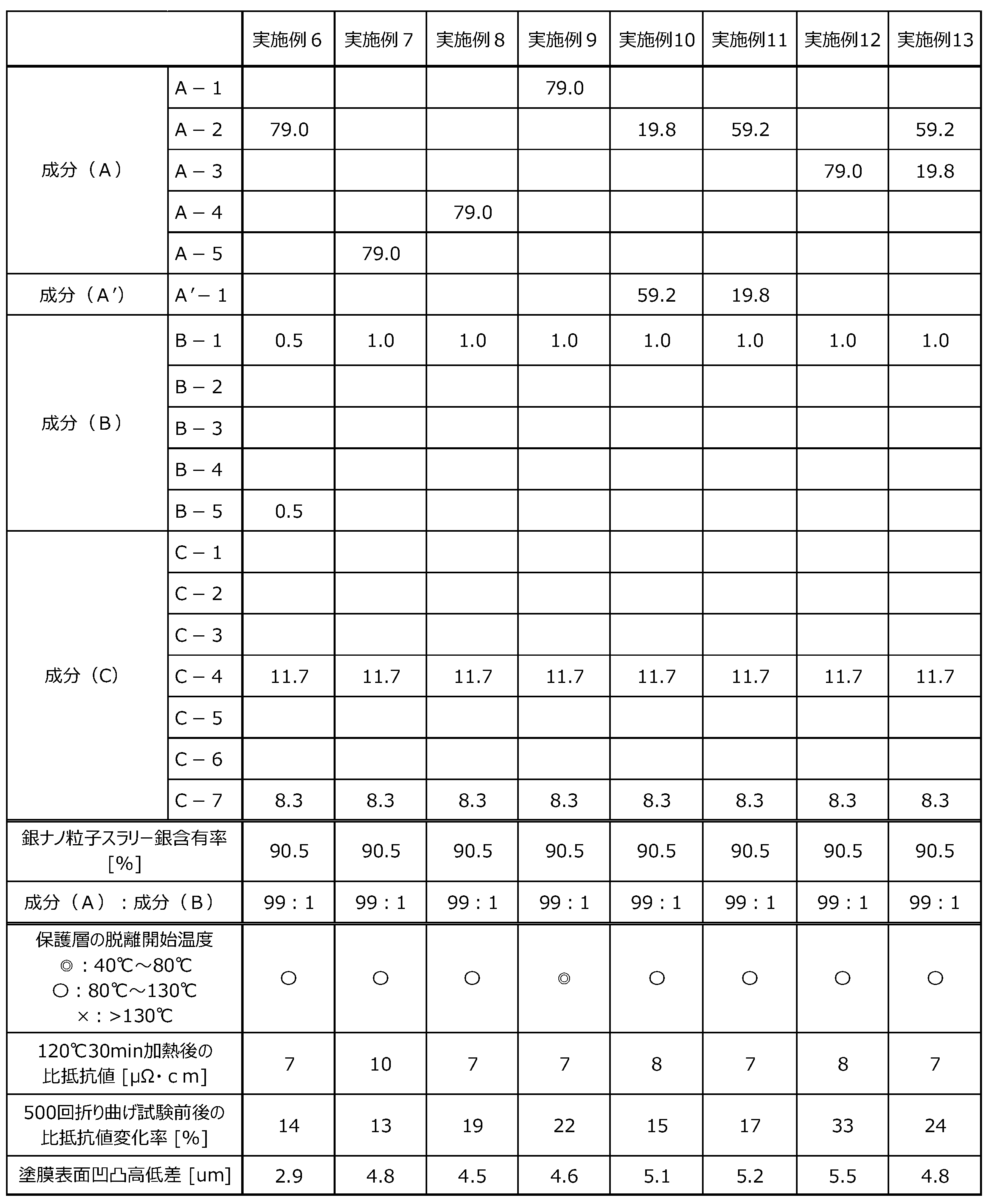
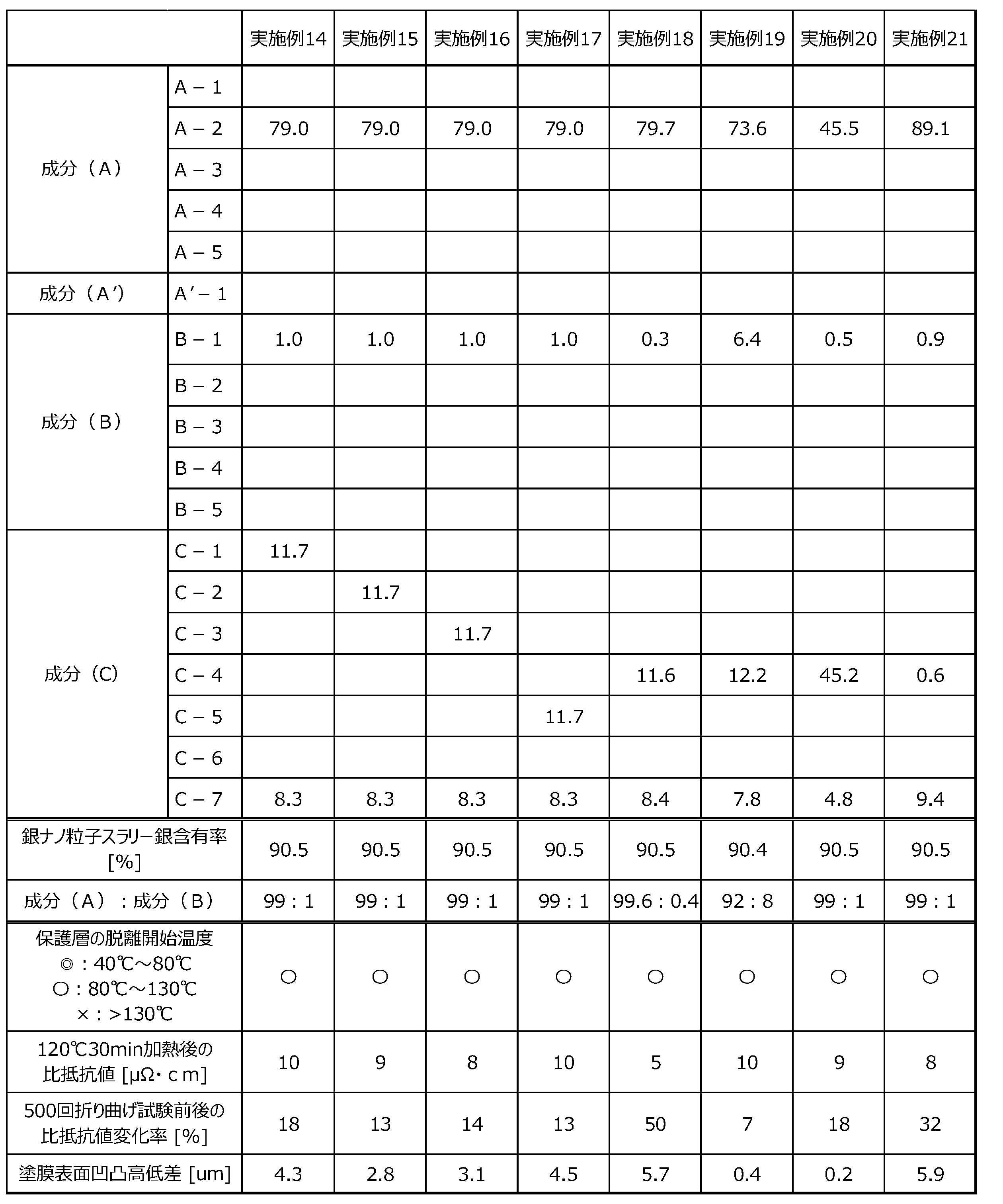
表面修飾銀ナノ粒子の保護層の脱離開始温度が130℃を超えた比較例2の導電性組成物は、比抵抗値が8×10⁻⁵Ω・cmと高かった。
(B)バインダー樹脂を含まない比較例3の導電性組成物の焼結膜は、500回折り曲げ試験において断線し、十分な曲げ耐性があるとは言えないものであった。また、表面凹凸高低差が6μmを超えた。
本明細書に記載された全ての文献、特許出願、および技術規格は、個々の文献、特許出願、および技術規格が参照により取り込まれることが具体的かつ個々に記された場合と同程度に、本明細書に参照により取り込まれる。
Claims (14)
- (A)表面が低級カルボン酸で被覆された表面修飾銀ナノ粒子と、
(B)バインダー樹脂と、
(C)有機溶剤と、
を含む導電性組成物であって、
導電性組成物中に存在する前記(A)表面修飾銀ナノ粒子の低級カルボン酸が、40℃~130℃で銀ナノ粒子から脱離開始する、導電性組成物。 - 前記(A)表面修飾銀ナノ粒子の中の低級カルボン酸が、酢酸、酪酸、乳酸、マレイン酸メチル及びヒドロキシイソ酪酸より選ばれる少なくとも1種である、請求項1に記載の導電性組成物。
- 前記(C)有機溶剤が、180℃~270℃の沸点を有する有機溶剤を含む、請求項1又は2に記載の導電性組成物。
- 前記(A)表面修飾銀ナノ粒子の平均粒子径が、20nm~600nmである、請求項1~3のいずれか1項に記載の導電性組成物。
- (B)バインダー樹脂の重量平均分子量が、5,000~200,000である、請求項1~4のいずれか1項に記載の導電性組成物。
- 前記(B)バインダー樹脂が、セルロース系樹脂である、請求項1~5のいずれか1項に記載の導電性組成物。
- 前記(A)表面修飾銀ナノ粒子と(B)バインダー樹脂との質量比(成分(A):成分(B))が、90:10~99.7:0.3である、請求項1~6のいずれか1項に記載の導電性組成物。
- 前記(C)有機溶剤の含有量が、導電性組成物100質量部に対して10質量部~50質量部である、請求項1~7のいずれか1項に記載の導電性組成物。
- 120℃30分の加熱条件において、比抵抗値が1.0×10⁻⁵Ω・cm以下である焼結膜を形成する、請求項1~8のいずれか1項に記載の導電性組成物。
- 折り曲げを500回繰り返す前後における比抵抗値変化率が50%以下である焼結膜を形成する、請求項1~9のいずれか1項に記載の導電性組成物。
- 120℃30分の加熱条件において、表面凹凸高低差が6μm以下である焼結膜を形成する、請求項1~10のいずれか1項に記載の導電性組成物。
- 請求項1~11のいずれか1項に記載の導電性組成物の焼結体。
- 請求項12に記載の焼結体を基材上に有する積層構造体。
- 請求項12に記載の焼結体を有する電子部品又は半導体装置。
Priority Applications (2)
| Application Number | Priority Date | Filing Date | Title |
|---|---|---|---|
| JP2024549839A JPWO2024070271A1 (ja) | 2022-09-27 | 2023-08-10 | |
| CN202380067678.9A CN119968441A (zh) | 2022-09-27 | 2023-08-10 | 导电性组合物、其烧结体、层叠结构体、电子部件及半导体装置 |
Applications Claiming Priority (2)
| Application Number | Priority Date | Filing Date | Title |
|---|---|---|---|
| JP2022153954 | 2022-09-27 | ||
| JP2022-153954 | 2022-09-27 |
Publications (1)
| Publication Number | Publication Date |
|---|---|
| WO2024070271A1 true WO2024070271A1 (ja) | 2024-04-04 |
Family
ID=90477043
Family Applications (1)
| Application Number | Title | Priority Date | Filing Date |
|---|---|---|---|
| PCT/JP2023/029218 Ceased WO2024070271A1 (ja) | 2022-09-27 | 2023-08-10 | 導電性組成物、その焼結体、積層構造体、電子部品及び半導体装置 |
Country Status (4)
| Country | Link |
|---|---|
| JP (1) | JPWO2024070271A1 (ja) |
| CN (1) | CN119968441A (ja) |
| TW (1) | TW202430293A (ja) |
| WO (1) | WO2024070271A1 (ja) |
Citations (3)
| Publication number | Priority date | Publication date | Assignee | Title |
|---|---|---|---|---|
| JP2011238596A (ja) * | 2010-04-14 | 2011-11-24 | Dowa Holdings Co Ltd | 熱硬化型導電性ペーストおよび配線基板 |
| WO2012060284A1 (ja) * | 2010-11-01 | 2012-05-10 | Dowaエレクトロニクス株式会社 | 低温焼結性導電性ペーストおよびそれを用いた導電膜と導電膜の形成方法 |
| WO2012147945A1 (ja) * | 2011-04-28 | 2012-11-01 | Dowaエレクトロニクス株式会社 | 平板状の銀微粒子とその製造方法およびそれを用いたペーストとペーストを用いた印刷回路 |
-
2023
- 2023-08-10 JP JP2024549839A patent/JPWO2024070271A1/ja active Pending
- 2023-08-10 CN CN202380067678.9A patent/CN119968441A/zh active Pending
- 2023-08-10 TW TW112130136A patent/TW202430293A/zh unknown
- 2023-08-10 WO PCT/JP2023/029218 patent/WO2024070271A1/ja not_active Ceased
Patent Citations (3)
| Publication number | Priority date | Publication date | Assignee | Title |
|---|---|---|---|---|
| JP2011238596A (ja) * | 2010-04-14 | 2011-11-24 | Dowa Holdings Co Ltd | 熱硬化型導電性ペーストおよび配線基板 |
| WO2012060284A1 (ja) * | 2010-11-01 | 2012-05-10 | Dowaエレクトロニクス株式会社 | 低温焼結性導電性ペーストおよびそれを用いた導電膜と導電膜の形成方法 |
| WO2012147945A1 (ja) * | 2011-04-28 | 2012-11-01 | Dowaエレクトロニクス株式会社 | 平板状の銀微粒子とその製造方法およびそれを用いたペーストとペーストを用いた印刷回路 |
Also Published As
| Publication number | Publication date |
|---|---|
| CN119968441A (zh) | 2025-05-09 |
| TW202430293A (zh) | 2024-08-01 |
| JPWO2024070271A1 (ja) | 2024-04-04 |
Similar Documents
| Publication | Publication Date | Title |
|---|---|---|
| CN113677458B (zh) | 混合银粉和包含其的导电糊 | |
| CN103597547B (zh) | 含有蜡触变胶的可高纵横比丝网印刷的厚膜糊剂组合物 | |
| JP5632176B2 (ja) | 積層体、この積層体を用いた導電性基材及びその製造方法 | |
| JP5558069B2 (ja) | 積層体、この積層体を用いた導電性基材及びその製造方法 | |
| TWI603342B (zh) | 導電膜形成用組成物及使用其的導電膜的製造方法 | |
| JP3541070B2 (ja) | 自動車ガラスの厚膜導電体ペースト | |
| KR102167706B1 (ko) | 잉크 조성물 및 잉크 조성물 경화도 판단 방법 | |
| JP6277751B2 (ja) | 銅粒子分散ペースト、及び導電性基板の製造方法 | |
| JP2015517184A (ja) | 印刷用銅ペースト組成物及びこれを用いた金属パターンの形成方法 | |
| JP2016106356A (ja) | 導電性ペースト及び導電膜の製造方法 | |
| WO2007083710A1 (ja) | 導電性ペースト及びそれを用いた配線基板 | |
| WO2014073530A1 (ja) | 導電性ペースト組成物 | |
| JP2017527943A (ja) | 導電性組成物 | |
| JPWO2016204105A1 (ja) | 金属ナノ微粒子製造用組成物 | |
| JP6117273B2 (ja) | 誘電体ガラス組成物 | |
| JP2014150061A (ja) | 低焼成銀導体 | |
| JP2009515023A (ja) | 金属インク、並びにそれを用いた電極形成方法及び基板 | |
| WO2016185728A1 (ja) | 銀ナノ粒子分散体の製造方法及び銀ナノ粒子インクの製造方法 | |
| JP5776180B2 (ja) | 導電性インク組成物、及びそれを用いて製造された電気的導通部位 | |
| JPWO2019069936A1 (ja) | 銀微粒子分散液 | |
| JP2014067492A (ja) | 導電部形成用組成物、及び導電部の製造方法 | |
| JP2012079457A (ja) | 導電性ペースト及び導電パターン | |
| CN106605270A (zh) | 含铜导电浆料和由此制成的电极 | |
| TWI567756B (zh) | 柔性基板用導電性糊組合物及其製備方法 | |
| TW202430293A (zh) | 導電性組成物、導電性組成物的燒結體、積層構造體、電子零件及半導體裝置 |
Legal Events
| Date | Code | Title | Description |
|---|---|---|---|
| 121 | Ep: the epo has been informed by wipo that ep was designated in this application |
Ref document number: 23871513 Country of ref document: EP Kind code of ref document: A1 |
|
| WWE | Wipo information: entry into national phase |
Ref document number: 2024549839 Country of ref document: JP |
|
| WWE | Wipo information: entry into national phase |
Ref document number: 202380067678.9 Country of ref document: CN |
|
| NENP | Non-entry into the national phase |
Ref country code: DE |
|
| WWP | Wipo information: published in national office |
Ref document number: 202380067678.9 Country of ref document: CN |
|
| 122 | Ep: pct application non-entry in european phase |
Ref document number: 23871513 Country of ref document: EP Kind code of ref document: A1 |