WO2024063122A1 - 電子部品又は半導体装置の製造方法 - Google Patents
電子部品又は半導体装置の製造方法 Download PDFInfo
- Publication number
- WO2024063122A1 WO2024063122A1 PCT/JP2023/034243 JP2023034243W WO2024063122A1 WO 2024063122 A1 WO2024063122 A1 WO 2024063122A1 JP 2023034243 W JP2023034243 W JP 2023034243W WO 2024063122 A1 WO2024063122 A1 WO 2024063122A1
- Authority
- WO
- WIPO (PCT)
- Prior art keywords
- adhesive layer
- manufacturing
- processed
- less
- treatment
- Prior art date
- Legal status (The legal status is an assumption and is not a legal conclusion. Google has not performed a legal analysis and makes no representation as to the accuracy of the status listed.)
- Ceased
Links
Images





Classifications
-
- C—CHEMISTRY; METALLURGY
- C09—DYES; PAINTS; POLISHES; NATURAL RESINS; ADHESIVES; COMPOSITIONS NOT OTHERWISE PROVIDED FOR; APPLICATIONS OF MATERIALS NOT OTHERWISE PROVIDED FOR
- C09J—ADHESIVES; NON-MECHANICAL ASPECTS OF ADHESIVE PROCESSES IN GENERAL; ADHESIVE PROCESSES NOT PROVIDED FOR ELSEWHERE; USE OF MATERIALS AS ADHESIVES
- C09J7/00—Adhesives in the form of films or foils
- C09J7/30—Adhesives in the form of films or foils characterised by the adhesive composition
- C09J7/38—Pressure-sensitive adhesives [PSA]
-
- C—CHEMISTRY; METALLURGY
- C09—DYES; PAINTS; POLISHES; NATURAL RESINS; ADHESIVES; COMPOSITIONS NOT OTHERWISE PROVIDED FOR; APPLICATIONS OF MATERIALS NOT OTHERWISE PROVIDED FOR
- C09J—ADHESIVES; NON-MECHANICAL ASPECTS OF ADHESIVE PROCESSES IN GENERAL; ADHESIVE PROCESSES NOT PROVIDED FOR ELSEWHERE; USE OF MATERIALS AS ADHESIVES
- C09J5/00—Adhesive processes in general; Adhesive processes not provided for elsewhere, e.g. relating to primers
-
- C—CHEMISTRY; METALLURGY
- C09—DYES; PAINTS; POLISHES; NATURAL RESINS; ADHESIVES; COMPOSITIONS NOT OTHERWISE PROVIDED FOR; APPLICATIONS OF MATERIALS NOT OTHERWISE PROVIDED FOR
- C09J—ADHESIVES; NON-MECHANICAL ASPECTS OF ADHESIVE PROCESSES IN GENERAL; ADHESIVE PROCESSES NOT PROVIDED FOR ELSEWHERE; USE OF MATERIALS AS ADHESIVES
- C09J7/00—Adhesives in the form of films or foils
- C09J7/10—Adhesives in the form of films or foils without carriers
-
- C—CHEMISTRY; METALLURGY
- C09—DYES; PAINTS; POLISHES; NATURAL RESINS; ADHESIVES; COMPOSITIONS NOT OTHERWISE PROVIDED FOR; APPLICATIONS OF MATERIALS NOT OTHERWISE PROVIDED FOR
- C09J—ADHESIVES; NON-MECHANICAL ASPECTS OF ADHESIVE PROCESSES IN GENERAL; ADHESIVE PROCESSES NOT PROVIDED FOR ELSEWHERE; USE OF MATERIALS AS ADHESIVES
- C09J7/00—Adhesives in the form of films or foils
- C09J7/30—Adhesives in the form of films or foils characterised by the adhesive composition
-
- H—ELECTRICITY
- H10—SEMICONDUCTOR DEVICES; ELECTRIC SOLID-STATE DEVICES NOT OTHERWISE PROVIDED FOR
- H10P—GENERIC PROCESSES OR APPARATUS FOR THE MANUFACTURE OR TREATMENT OF DEVICES COVERED BY CLASS H10
- H10P54/00—Cutting or separating of wafers, substrates or parts of devices
-
- H—ELECTRICITY
- H10—SEMICONDUCTOR DEVICES; ELECTRIC SOLID-STATE DEVICES NOT OTHERWISE PROVIDED FOR
- H10P—GENERIC PROCESSES OR APPARATUS FOR THE MANUFACTURE OR TREATMENT OF DEVICES COVERED BY CLASS H10
- H10P72/00—Handling or holding of wafers, substrates or devices during manufacture or treatment thereof
- H10P72/70—Handling or holding of wafers, substrates or devices during manufacture or treatment thereof for supporting or gripping
-
- H—ELECTRICITY
- H10—SEMICONDUCTOR DEVICES; ELECTRIC SOLID-STATE DEVICES NOT OTHERWISE PROVIDED FOR
- H10P—GENERIC PROCESSES OR APPARATUS FOR THE MANUFACTURE OR TREATMENT OF DEVICES COVERED BY CLASS H10
- H10P72/00—Handling or holding of wafers, substrates or devices during manufacture or treatment thereof
- H10P72/70—Handling or holding of wafers, substrates or devices during manufacture or treatment thereof for supporting or gripping
- H10P72/74—Handling or holding of wafers, substrates or devices during manufacture or treatment thereof for supporting or gripping using temporarily an auxiliary support
- H10P72/7402—Wafer tapes, e.g. grinding or dicing support tapes
-
- H—ELECTRICITY
- H10—SEMICONDUCTOR DEVICES; ELECTRIC SOLID-STATE DEVICES NOT OTHERWISE PROVIDED FOR
- H10P—GENERIC PROCESSES OR APPARATUS FOR THE MANUFACTURE OR TREATMENT OF DEVICES COVERED BY CLASS H10
- H10P72/00—Handling or holding of wafers, substrates or devices during manufacture or treatment thereof
- H10P72/70—Handling or holding of wafers, substrates or devices during manufacture or treatment thereof for supporting or gripping
- H10P72/74—Handling or holding of wafers, substrates or devices during manufacture or treatment thereof for supporting or gripping using temporarily an auxiliary support
- H10P72/7412—Handling or holding of wafers, substrates or devices during manufacture or treatment thereof for supporting or gripping using temporarily an auxiliary support the auxiliary support including means facilitating the separation of a device or wafer from the auxiliary support
- H10P72/7414—Handling or holding of wafers, substrates or devices during manufacture or treatment thereof for supporting or gripping using temporarily an auxiliary support the auxiliary support including means facilitating the separation of a device or wafer from the auxiliary support the auxiliary support including means facilitating the selective separation of some of a plurality of devices from the auxiliary support
-
- H—ELECTRICITY
- H10—SEMICONDUCTOR DEVICES; ELECTRIC SOLID-STATE DEVICES NOT OTHERWISE PROVIDED FOR
- H10P—GENERIC PROCESSES OR APPARATUS FOR THE MANUFACTURE OR TREATMENT OF DEVICES COVERED BY CLASS H10
- H10P95/00—Generic processes or apparatus for manufacture or treatments not covered by the other groups of this subclass
-
- H—ELECTRICITY
- H10—SEMICONDUCTOR DEVICES; ELECTRIC SOLID-STATE DEVICES NOT OTHERWISE PROVIDED FOR
- H10W—GENERIC PACKAGES, INTERCONNECTIONS, CONNECTORS OR OTHER CONSTRUCTIONAL DETAILS OF DEVICES COVERED BY CLASS H10
- H10W74/00—Encapsulations, e.g. protective coatings
- H10W74/01—Manufacture or treatment
-
- H—ELECTRICITY
- H10—SEMICONDUCTOR DEVICES; ELECTRIC SOLID-STATE DEVICES NOT OTHERWISE PROVIDED FOR
- H10W—GENERIC PACKAGES, INTERCONNECTIONS, CONNECTORS OR OTHER CONSTRUCTIONAL DETAILS OF DEVICES COVERED BY CLASS H10
- H10W74/00—Encapsulations, e.g. protective coatings
- H10W74/01—Manufacture or treatment
- H10W74/014—Manufacture or treatment using batch processing
-
- H—ELECTRICITY
- H10—SEMICONDUCTOR DEVICES; ELECTRIC SOLID-STATE DEVICES NOT OTHERWISE PROVIDED FOR
- H10W—GENERIC PACKAGES, INTERCONNECTIONS, CONNECTORS OR OTHER CONSTRUCTIONAL DETAILS OF DEVICES COVERED BY CLASS H10
- H10W74/00—Encapsulations, e.g. protective coatings
- H10W74/01—Manufacture or treatment
- H10W74/019—Manufacture or treatment using temporary auxiliary substrates
-
- C—CHEMISTRY; METALLURGY
- C09—DYES; PAINTS; POLISHES; NATURAL RESINS; ADHESIVES; COMPOSITIONS NOT OTHERWISE PROVIDED FOR; APPLICATIONS OF MATERIALS NOT OTHERWISE PROVIDED FOR
- C09J—ADHESIVES; NON-MECHANICAL ASPECTS OF ADHESIVE PROCESSES IN GENERAL; ADHESIVE PROCESSES NOT PROVIDED FOR ELSEWHERE; USE OF MATERIALS AS ADHESIVES
- C09J2203/00—Applications of adhesives in processes or use of adhesives in the form of films or foils
- C09J2203/326—Applications of adhesives in processes or use of adhesives in the form of films or foils for bonding electronic components such as wafers, chips or semiconductors
-
- C—CHEMISTRY; METALLURGY
- C09—DYES; PAINTS; POLISHES; NATURAL RESINS; ADHESIVES; COMPOSITIONS NOT OTHERWISE PROVIDED FOR; APPLICATIONS OF MATERIALS NOT OTHERWISE PROVIDED FOR
- C09J—ADHESIVES; NON-MECHANICAL ASPECTS OF ADHESIVE PROCESSES IN GENERAL; ADHESIVE PROCESSES NOT PROVIDED FOR ELSEWHERE; USE OF MATERIALS AS ADHESIVES
- C09J2301/00—Additional features of adhesives in the form of films or foils
- C09J2301/20—Additional features of adhesives in the form of films or foils characterized by the structural features of the adhesive itself
-
- C—CHEMISTRY; METALLURGY
- C09—DYES; PAINTS; POLISHES; NATURAL RESINS; ADHESIVES; COMPOSITIONS NOT OTHERWISE PROVIDED FOR; APPLICATIONS OF MATERIALS NOT OTHERWISE PROVIDED FOR
- C09J—ADHESIVES; NON-MECHANICAL ASPECTS OF ADHESIVE PROCESSES IN GENERAL; ADHESIVE PROCESSES NOT PROVIDED FOR ELSEWHERE; USE OF MATERIALS AS ADHESIVES
- C09J2301/00—Additional features of adhesives in the form of films or foils
- C09J2301/30—Additional features of adhesives in the form of films or foils characterized by the chemical, physicochemical or physical properties of the adhesive or the carrier
- C09J2301/302—Additional features of adhesives in the form of films or foils characterized by the chemical, physicochemical or physical properties of the adhesive or the carrier the adhesive being pressure-sensitive, i.e. tacky at temperatures inferior to 30°C
-
- C—CHEMISTRY; METALLURGY
- C09—DYES; PAINTS; POLISHES; NATURAL RESINS; ADHESIVES; COMPOSITIONS NOT OTHERWISE PROVIDED FOR; APPLICATIONS OF MATERIALS NOT OTHERWISE PROVIDED FOR
- C09J—ADHESIVES; NON-MECHANICAL ASPECTS OF ADHESIVE PROCESSES IN GENERAL; ADHESIVE PROCESSES NOT PROVIDED FOR ELSEWHERE; USE OF MATERIALS AS ADHESIVES
- C09J2301/00—Additional features of adhesives in the form of films or foils
- C09J2301/50—Additional features of adhesives in the form of films or foils characterized by process specific features
- C09J2301/502—Additional features of adhesives in the form of films or foils characterized by process specific features process for debonding adherents
-
- H—ELECTRICITY
- H10—SEMICONDUCTOR DEVICES; ELECTRIC SOLID-STATE DEVICES NOT OTHERWISE PROVIDED FOR
- H10P—GENERIC PROCESSES OR APPARATUS FOR THE MANUFACTURE OR TREATMENT OF DEVICES COVERED BY CLASS H10
- H10P72/00—Handling or holding of wafers, substrates or devices during manufacture or treatment thereof
- H10P72/70—Handling or holding of wafers, substrates or devices during manufacture or treatment thereof for supporting or gripping
- H10P72/74—Handling or holding of wafers, substrates or devices during manufacture or treatment thereof for supporting or gripping using temporarily an auxiliary support
-
- H—ELECTRICITY
- H10—SEMICONDUCTOR DEVICES; ELECTRIC SOLID-STATE DEVICES NOT OTHERWISE PROVIDED FOR
- H10P—GENERIC PROCESSES OR APPARATUS FOR THE MANUFACTURE OR TREATMENT OF DEVICES COVERED BY CLASS H10
- H10P72/00—Handling or holding of wafers, substrates or devices during manufacture or treatment thereof
- H10P72/70—Handling or holding of wafers, substrates or devices during manufacture or treatment thereof for supporting or gripping
- H10P72/74—Handling or holding of wafers, substrates or devices during manufacture or treatment thereof for supporting or gripping using temporarily an auxiliary support
- H10P72/7412—Handling or holding of wafers, substrates or devices during manufacture or treatment thereof for supporting or gripping using temporarily an auxiliary support the auxiliary support including means facilitating the separation of a device or wafer from the auxiliary support
-
- H—ELECTRICITY
- H10—SEMICONDUCTOR DEVICES; ELECTRIC SOLID-STATE DEVICES NOT OTHERWISE PROVIDED FOR
- H10P—GENERIC PROCESSES OR APPARATUS FOR THE MANUFACTURE OR TREATMENT OF DEVICES COVERED BY CLASS H10
- H10P72/00—Handling or holding of wafers, substrates or devices during manufacture or treatment thereof
- H10P72/70—Handling or holding of wafers, substrates or devices during manufacture or treatment thereof for supporting or gripping
- H10P72/74—Handling or holding of wafers, substrates or devices during manufacture or treatment thereof for supporting or gripping using temporarily an auxiliary support
- H10P72/7416—Handling or holding of wafers, substrates or devices during manufacture or treatment thereof for supporting or gripping using temporarily an auxiliary support used during dicing or grinding
-
- H—ELECTRICITY
- H10—SEMICONDUCTOR DEVICES; ELECTRIC SOLID-STATE DEVICES NOT OTHERWISE PROVIDED FOR
- H10P—GENERIC PROCESSES OR APPARATUS FOR THE MANUFACTURE OR TREATMENT OF DEVICES COVERED BY CLASS H10
- H10P72/00—Handling or holding of wafers, substrates or devices during manufacture or treatment thereof
- H10P72/70—Handling or holding of wafers, substrates or devices during manufacture or treatment thereof for supporting or gripping
- H10P72/74—Handling or holding of wafers, substrates or devices during manufacture or treatment thereof for supporting or gripping using temporarily an auxiliary support
- H10P72/744—Details of chemical or physical process used for separating the auxiliary support from a device or a wafer
-
- H—ELECTRICITY
- H10—SEMICONDUCTOR DEVICES; ELECTRIC SOLID-STATE DEVICES NOT OTHERWISE PROVIDED FOR
- H10W—GENERIC PACKAGES, INTERCONNECTIONS, CONNECTORS OR OTHER CONSTRUCTIONAL DETAILS OF DEVICES COVERED BY CLASS H10
- H10W74/00—Encapsulations, e.g. protective coatings
- H10W74/01—Manufacture or treatment
- H10W74/016—Manufacture or treatment using moulds
Definitions
- the present invention relates to a method of manufacturing an electronic component or a semiconductor device, and relates to a technique for sealing a semiconductor element, for example.
- processing is performed on objects to be processed, such as encapsulation of elements or wiring, as described in Patent Document 1, for example.
- objects to be processed such as encapsulation of elements or wiring, as described in Patent Document 1, for example.
- processing of the object to be processed is often performed while the object is attached to a pressure-sensitive adhesive sheet.
- Patent Document 1 proposes adding thermally expandable particles to an adhesive in order to facilitate the removal of elements and increase productivity.
- An object of the present invention is to provide a new method for facilitating the removal of processed products and increasing productivity when manufacturing electronic components or semiconductor devices.
- the inventor of the present invention has found that by attaching the object to be treated to the uneven surface of the adhesive layer and then processing the object, it is possible to easily remove the treated object and increase productivity.
- the inventors have discovered that the above-mentioned problems can be solved, and after conducting various studies, they have completed the present invention.
- the present invention relates to the following [1] to [13].
- a step of attaching a workpiece used for manufacturing electronic components or semiconductor devices to an uneven surface of an adhesive layer A step of obtaining a processed product by performing a process on the object to be processed on the adhesive layer; removing the processed product from the adhesive layer;
- a method for manufacturing an electronic component or a semiconductor device comprising: [2] The manufacturing method according to [1], wherein the workpiece is an element, a semiconductor wafer, or a panel.
- the treatment of the object to be treated includes an energy application treatment, a liquid contact treatment, a vacuum treatment, or a sealing treatment.
- the object to be treated on the adhesive layer is sealed with a sealant to form a sealed body
- the manufacturing method according to [1] wherein in the removing step, the sealing body including the object to be treated is removed from the adhesive layer.
- the sealant is formed so that the sealant is in contact with both the object to be treated and the uneven surface of the adhesive layer.
- the manufacturing method according to [6] in the step of carrying out the processing, two or more of the objects to be processed are sealed together and then further singulated.
- the step of attaching the workpiece includes a step of capturing the workpiece separated from the holding substrate in the adhesive layer.
- the adhesive layer comprises a substrate and an adhesive layer formed on the substrate and having an uneven surface.
- the adhesive layer has a plurality of convex portions on the surface thereof that are spaced apart from each other via concave portions.
- the adhesive layer has protrusions bounded by recesses, The manufacturing method according to any one of [1] to [9], wherein the ratio of the area occupied by the convex portion to the area of the adhesive layer is 1% or more and 95% or less. [12] The manufacturing method described in any one of [1] to [9], wherein the adhesive layer is configured so that the ratio of the adhesion area between the adhesive layer and one of the workpieces to the area of one of the workpieces is 1% or more and 95% or less. [13] The manufacturing method according to any one of [1] to [9], wherein the area of the workpiece is 100 mm2 or less.
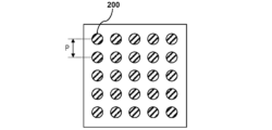
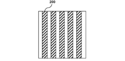
- FIG. 4 is a top view showing an example of unevenness of an adhesive layer.
- FIG. 4 is a top view showing an example of unevenness of an adhesive layer.
- FIG. 4 is a top view showing an example of unevenness of an adhesive layer.
- FIG. 4 is a cross-sectional view showing an example of projections and recesses on an adhesive layer.
- FIG. 4 is a cross-sectional view showing an example of projections and recesses on an adhesive layer.
- FIG. 4 is a cross-sectional view showing an example of projections and recesses on an adhesive layer.
- 1A to 1C are diagrams for explaining separation and capture of elements.
- 1A to 1C are diagrams for explaining separation and capture of elements.
- 1 is a flowchart of a manufacturing method according to an embodiment.
- 1A to 1C are diagrams illustrating a manufacturing method according to an embodiment.
- 1A to 1C are diagrams illustrating a manufacturing method according to an embodiment.
- 1A to 1C are diagrams illustrating a manufacturing method according to an embodiment.
- 1A to 1C are diagrams illustrating a manufacturing method according to an embodiment.
- FIG. 2 is a diagram for explaining an apparent contact angle.
- mass average molecular weight (Mw) and number average molecular weight (Mn) are values measured by size exclusion chromatography in terms of standard polystyrene, specifically based on JIS K7252-1:2016. It is the value to be measured.
- (meth)acrylic is a term that refers to both "acrylic” and “methacrylic”.
- electrosenor parts includes all parts used in electronic engineering, electrical engineering, etc., and all parts constituting electronic equipment.
- the “electronic component” may be formed of a semiconductor, a conductor, and/or an insulator, or a combination of these.
- Examples of “electronic components” include active components (mainly made of semiconductors, such as transistors, ICs, LSIs, VLSIs, diodes, light-emitting diodes, thyristors, three-terminal regulators, and image sensors, etc.), passive devices, etc. (e.g.
- semiconductor device refers to all devices used in processors, memories, sensors, etc., which can function by utilizing semiconductor characteristics. Examples of “semiconductor devices” include micro light emitting diodes, mini light emitting diodes, power devices, MEMS (Micro Electro Mechanical Systems), controller chips, and the like.
- any combination of the lower limit value and upper limit value among them is described.
- the description of preferably 1 or more, more preferably 2 or more, still more preferably 3 or more, preferably 9 or less, more preferably 8 or less, still more preferably 7 or less means that the numerical range is 1 or more 9 or less, 1 or more and 8 or less, 1 or more and 7 or less, 2 or more and 9 or less, 2 or more and 8 or less, 2 or more and 7 or less, 3 or more and 9 or less, 3 or more and 8 or less, and 3 or more and 7 or less. It clearly means that.
- an adhesive layer having an uneven surface is used.
- a treatment is performed on an object to be treated stuck on an adhesive layer.
- the element separated from the holding substrate may be captured on the adhesive layer in order to adhere the object to be processed on the adhesive layer.
- the adhesive layer may be provided on the base material.
- an adhesive sheet including a base material 110 and an adhesive layer 120 can be used.
- the treatment can be performed on the object stuck on the adhesive layer 120 of the adhesive sheet.
- the adhesive sheet may be composed of only the adhesive layer 120. In this case, a highly supportive adhesive layer 120 can be used.
- the substrate 110 functions as a support for the adhesive layer 120.
- the type of substrate 110 is not particularly limited, and may be a hard substrate or a flexible substrate. From the viewpoint of facilitating attachment to other members such as a substrate, improving peelability, facilitating lamination, or enabling formation into a roll form, it is preferable that the substrate 110 is a flexible substrate.
- a resin film may be used as the substrate 110.
- the resin film is a film in which a resin material is used as the main material, and may be made of the resin material, or may contain additives in addition to the resin material.
- the resin film may have laser light transmittance.
- resin films include polyethylene films such as low density polyethylene (LDPE) films, linear low density polyethylene (LLDPE) films, and high density polyethylene (HDPE) films, polypropylene films, polybutene films, polybutadiene films, and polymethyl.
- LDPE low density polyethylene
- LLDPE linear low density polyethylene
- HDPE high density polyethylene
- Polyolefin films such as pentene film, ethylene-norbornene copolymer film, and norbornene resin film; ethylene-vinyl acetate copolymer film, ethylene-(meth)acrylic acid copolymer film, and ethylene-(meth)acrylic acid film Ethylene copolymer films such as ester copolymer films; polyvinyl chloride films such as polyvinyl chloride films and vinyl chloride copolymer films; polyester films such as polyethylene terephthalate films and polybutylene terephthalate films; polyurethane films; Examples include polyimide film; polystyrene film; polycarbonate film; and fluororesin film.
- modified films such as films containing mixtures of two or more materials, crosslinked films in which the resins forming these films are crosslinked, and ionomer films may be used.
- the base material 110 may be a laminated film in which two or more types of resin films are laminated.
- the resin film may be a single-layer film selected from the group consisting of polyethylene film, polyester film, and polypropylene film. Or, it is preferable that it is a laminated film in which two or more types of films selected from this group are laminated.
- the thickness of the base material 110 is not particularly limited, but from the viewpoint of achieving both supportability and rollability, it is preferably in the range of 10 ⁇ m to 500 ⁇ m, more preferably 25 ⁇ m to 200 ⁇ m, and even more preferably 40 ⁇ m to 90 ⁇ m.
- the adhesive layer 120 is a layer having adhesiveness and can contain resin. Further, the surface of the adhesive layer 120 has irregularities. Note that the adhesive sheet may have two or more adhesive layers 120. For example, the adhesive sheet may have a laminate of one or more types of adhesive layers 120.
- composition of adhesive layer examples include rubber resins such as polyisobutylene resins, polybutadiene resins, and styrene-butadiene resins, acrylic resins, urethane resins, polyester resins, olefin resins, and silicone resins. , and polyvinyl ether resins.
- the adhesive layer may have heat resistance, and examples of materials for the adhesive layer having such heat resistance include polyimide resins and silicone resins.
- the adhesive layer may contain a copolymer having two or more types of structural units. The form of such a copolymer is not particularly limited, and may be any of a block copolymer, random copolymer, alternating copolymer, and graft copolymer.
- the resin contained in the adhesive layer 120 is an adhesive resin that has adhesive properties by itself.
- the resin is preferably a polymer having a mass average molecular weight (Mw) of 10,000 or more.
- the weight average molecular weight (Mw) of the resin is preferably 10,000 or more, more preferably 70,000 or more, and even more preferably 140,000 or more from the viewpoint of improving adhesive strength.
- it is preferably 2,000,000 or less, more preferably 1,200,000 or less, and even more preferably 900,000 or less.
- the number average molecular weight (Mn) of the resin is preferably 10,000 or more, more preferably 50,000 or more, and even more preferably 100,000 or more from the viewpoint of improving adhesive strength. Moreover, from the viewpoint of suppressing the storage elastic modulus to a predetermined value or less, it is preferably 2,000,000 or less, more preferably 1,000,000 or less, and even more preferably 700,000 or less.
- the mass average molecular weight (Mw) and number average molecular weight (Mn) are the mass average molecular weight (Mw) before crosslinking reaction due to energy application. and number average molecular weight (Mn).
- the glass transition temperature (Tg) of the resin is preferably -70°C or higher, more preferably -60°C or higher, and preferably -10°C or lower, more preferably -20°C or lower.
- Tg glass transition temperature
- the amount of resin included in the adhesive layer 120 relative to the total amount of components constituting the adhesive layer 120 can be appropriately set depending on the required adhesive strength and storage modulus of the adhesive layer 120, but is preferably 30% by mass or more. , more preferably 40% by mass or more, still more preferably 50% by mass or more, still more preferably 55% by mass or more, even more preferably 60% by mass or more, and preferably 99.99% by mass or less, more preferably 99.95% by mass. It is not more than 99.90% by mass, even more preferably not more than 99.80% by mass, even more preferably not more than 99.50% by mass.
- the resin contained in the adhesive layer 120 is preferably derived from an energy-reactive resin.
- Energy-responsive resin refers to a resin whose elastic modulus improves when energy is applied.
- Energy-reactive resins include energy-ray-reactive resins and heat-reactive resins.
- Energy ray-reactive resin refers to a resin whose elastic modulus is improved by irradiation with energy rays.
- thermalally reactive resin refers to a resin whose elastic modulus is improved by heating.
- the type of energy ray is not particularly limited, and examples thereof include ultraviolet rays, electron beams, and ionizing radiation.
- the energy beam is preferably ultraviolet rays, that is, the resin is preferably an ultraviolet-reactive resin.
- the resin is derived from an energy-responsive resin
- the resin is obtained from an energy-responsive resin.
- a resin derived from an energy-responsive resin is a crosslinked energy-responsive resin.
- the formed uneven shape can be easily maintained by applying energy (for example, irradiating with energy rays) after forming unevenness on the resin.
- the adhesive layer may contain components other than resin.
- the adhesive layer may contain one or more of a tackifier, a polymerization initiator, a UV absorber, and other additives.
- a polymerization initiator is a component that initiates a crosslinking reaction in response to application of energy (for example, irradiation with energy rays).
- energy for example, irradiation with energy rays.
- the adhesive layer contains an energy-reactive resin
- the adhesive layer further contains a polymerization initiator, so that the crosslinking reaction proceeds even when relatively low energy is applied.
- a photopolymerization initiator for example, a photopolymerization initiator can be used.
- the photopolymerization initiator include 1-hydroxycyclohexylphenyl ketone, benzoin, benzoin methyl ether, benzoin ethyl ether, benzoin propyl ether, benzylphenyl sulfide, tetramethylthiuram monosulfide, azobisisobutyronitrile, and dibenzyl. , diacetyl, and 8-chloroanthraquinone.
- the adhesive layer may contain one type of polymerization initiator, or may contain two or more types of polymerization initiator.
- the content of the polymerization initiator in the adhesive layer is preferably 0.01% by mass or more, more preferably 0.1% by mass, from the viewpoint of allowing the crosslinking reaction to proceed at an appropriate rate. It is at least 1% by mass, more preferably at least 1% by mass, preferably at most 10% by mass, more preferably at most 5% by mass, even more preferably at most 2% by mass.
- UV absorber examples include benzotriazole compounds, oxazolic acid amide compounds, and benzophenone compounds.
- additives that the adhesive layer may contain are not particularly limited, but include, for example, light stabilizers such as hindered amines, benzophenones, or benzotriazoles, phenolics such as hindered phenolic compounds, and aromatic additives.
- light stabilizers such as hindered amines, benzophenones, or benzotriazoles
- phenolics such as hindered phenolic compounds
- aromatic additives include, for example, light stabilizers such as hindered amines, benzophenones, or benzotriazoles
- phenolics such as hindered phenolic compounds
- aromatic additives aromatic additives.
- Amine-based, sulfur-based, or phosphorus-based antioxidants such as phosphate ester compounds, imidazole-based resin stabilizers, dithiocarbamate-based resin stabilizers, phosphorus-based resin stabilizers, or sulfur ester-based resin stabilizers
- resin stabilizers such as fillers, pigments, extenders,
- the content of the additives in the adhesive layer is preferably 0.0001% by mass or more, more preferably 0.01% by mass or more, particularly preferably 0.1% by mass or more, even more preferably 1% by mass or more, and is preferably 20% by mass or less, more preferably 10% by mass or less, even more preferably 5% by mass or less.
- the surface of the adhesive layer has irregularities. As will be described later, after the treatment object adhered to the adhesive layer is processed, the treatment object is removed from the adhesive layer. If the surface of the adhesive layer is flat, the adhesive layer and the object to be treated are in close contact with each other. At this time, even if you try to remove the object from the adhesive layer, it is difficult for air to enter between the adhesive layer and the object, so a sufficiently large force is required to remove the object from the adhesive layer. . On the other hand, since a gap exists between the adhesive layer having an uneven surface and the object to be treated, the object to be treated can be easily removed from the adhesive layer.
- the workpiece separated from the holding substrate can be captured by the adhesive layer.
- the adhesive layer can capture the workpiece at the convex parts.
- the gas compressed between the workpiece and the adhesive layer as the workpiece and the adhesive layer approach each other can escape to the concave parts of the adhesive layer.
- the adhesive layer has concaves and convexes, which can reduce the pressure generated between the workpiece and the adhesive layer. Therefore, it is also possible to prevent the pressure generated between the workpiece and the adhesive layer from shifting the holding position of the workpiece on the adhesive layer.
- the force required to remove the object from the adhesive layer can be adjusted by controlling the contact area between the object and the adhesive layer. Become. Moreover, if the surface of the adhesive layer has a recessed portion, the pressure generated between the object to be processed and the adhesive layer can be alleviated. Therefore, the specific shape of the unevenness on the surface of the adhesive layer is not limited.
- the adhesive layer has a plurality of protrusions on its surface that are spaced apart from each other via recesses.
- Each of the plurality of convex portions may be separated by a concave portion that is continuous throughout the adhesive layer.
- the recesses located around each of the plurality of projections are continuous to the end of the adhesive layer. In this way, by providing a concave portion that continues to the end of the adhesive layer, air can more easily enter between the object to be processed and the adhesive layer.
- FIGS. 2A to 2C are top views showing the shape of such an adhesive layer.
- convex portions may be regularly arranged on the surface of the adhesive layer.
- the convex portions being regularly arranged means that the convex portions are arranged in a straight line at regular intervals.
- the convex portions may be arranged so that the intervals vary regularly.
- the distance between the convex portions is short at the center of the adhesive layer, and the distance between the convex portions is long at the periphery of the adhesive layer. According to such a configuration, while increasing the holding power of the adhesive layer, air can easily enter between the adhesive layer and the object to be processed via the wide recess from the periphery of the object to be processed, which further reduces pressure. It can be efficiently released from the periphery of the processed material.
- the convex portions may be arranged irregularly.
- FIG. 2C is a top view showing another shape of the adhesive layer. As shown in FIG. 2C, striped convex portions may be provided on the surface of the adhesive layer. In FIG. 2C, linear convex portions having a constant width are lined up at regular intervals. On the other hand, as in FIG. 2B, the width or interval of the linear protrusions may vary regularly, or the linear protrusions may be arranged irregularly.
- the pitch of the convex portions is preferably 1 ⁇ m or more, more preferably 5 ⁇ m or more, and even more preferably 10 ⁇ m or more, from the viewpoint of facilitating the removal of the object to be treated or enhancing the pressure relief effect. More preferably, it is 15 ⁇ m or more.
- the pitch of the convex parts means the minimum interval among all the intervals of the convex parts in the entire adhesive layer.
- the pitch of the convex portions represents the interval between the convex portions on a straight line in which the convex portions are arranged at regular intervals.
- the pitch represents the interval between the protrusions on the straight line in which the protrusions are lined up at the shortest interval. Further, in the case of FIG. 2C, the pitch of the convex portions represents the interval between the linear convex portions.
- the distance between the convex portions means the distance between the centers of the convex portions.
- the contact area between the adhesive layer and the object to be processed can be increased, suppressing misalignment during capture.
- the object to be processed on the adhesive is sealed with a sealant.
- the wettability of the sealant to the surface of the adhesive layer before hardening is reduced, and the sealant is less likely to penetrate into the unevenness. This phenomenon of reduced wettability on a surface with a fine structure is generally called the lotus effect.
- the pitch of the protrusions is preferably 100 ⁇ m or less, more preferably 75 ⁇ m or less, even more preferably 50 ⁇ m or less, even more preferably 35 ⁇ m or less, and even more preferably 25 ⁇ m or less.
- the minimum spacing among all the protrusion spacings in the center of the adhesive layer may be shorter than the minimum spacing among all the protrusion spacings in the peripheral portion of the adhesive layer.
- the center is, for example, a circular region having 1/4 of the area of the adhesive layer and centered on the center of gravity of the adhesive layer
- the peripheral portion is, for example, the entire area of the adhesive layer other than the center.
- the convex portion may have a pillar shape.
- the convex portion may have a cylindrical shape or a prismatic shape.
- the convex portion may extend in a line shape, or may extend in a curved shape such as a wave shape.
- these convex portions may be provided with a taper.
- FIG. 3A shows a cross-sectional view of the adhesive layer according to one embodiment, passing through the convex portion and perpendicular to the surface of the adhesive layer.
- the convex portion shown in FIG. 3A is tapered, that is, the convex portion is tapered.
- the tip of the convex portion may be a curved surface. With this configuration, the impact when the adhesive layer comes into contact with the workpiece separated from the holding substrate is more relaxed, so the adhesive layer can easily hold the workpiece so that it does not shift. become. On the other hand, the tip of the convex portion may be flat.
- the surface of the adhesive layer may have flat recesses and protrusions protruding from the recesses.
- the plurality of convex portions that the adhesive layer has and are spaced apart from each other may be bounded by concave portions.
- the convex portion may be hemispherical or part of a sphere, as shown in FIG. 3B. Further, the convex portion may be T-shaped as shown in FIG. 3C. As yet another example, the convex portion may have a shape in which a plurality of grains are gathered together, a mushroom shape, a surface shape of a lotus leaf, or a needle shape. As yet another example, the surface of the adhesive layer may be rough or fibrous, and such a surface can also be said to have irregularities.
- each convex portion is preferably 1 ⁇ m or more, more preferably 2 ⁇ m or more, even more preferably 5 ⁇ m or more, and preferably 10 ⁇ m or more from the viewpoint of maintaining adhesiveness. More preferred.
- the width or diameter of each convex portion is preferably 100 ⁇ m or less, more preferably 50 ⁇ m or less, and 30 ⁇ m or less, from the viewpoint of facilitating the removal of the object to be treated or enhancing the pressure relief effect. It is more preferable that it is, and it is even more preferable that it is 20 ⁇ m or less.
- the width and diameter of the convex portion respectively mean the minimum distance and maximum distance (represented by B in FIG. 3A) between two parallel lines touching from both sides of the convex portion on the surface of the concave portion.
- the area of each convex portion is preferably 10 ⁇ m 2 or more, more preferably 20 ⁇ m 2 or more, and even more preferably 30 ⁇ m 2 or more.
- the area of each convex portion is preferably 2000 ⁇ m 2 or less, more preferably 1000 ⁇ m 2 or less, and 500 ⁇ m 2 from the viewpoint of facilitating the removal of the object to be treated or enhancing the pressure relief effect. It is more preferable that it is the following.
- the area of the convex portion means the area of the portion protruding from the surface of the concave portion (in the case of FIG. 3A, the area of a circle with diameter B).
- each convex portion is preferably 1 ⁇ m or more, more preferably 3 ⁇ m or more, and even more preferably 5 ⁇ m or more, from the viewpoint of making it easier for air to enter the recess.
- the height of each convex portion is preferably 20 ⁇ m or less, more preferably 15 ⁇ m or less, and even more preferably 10 ⁇ m or less.
- the height of the convex portion is represented by H in FIG. 3A.
- the area occupied by the plurality of convex portions relative to the area of the adhesive layer is preferably 1% or more, more preferably 5% or more, and 10% or more. is more preferable, more preferably 18% or more, even more preferably 40% or more.
- the area of each convex portion is preferably 95% or less, more preferably 75% or less, and even more preferably 60% or less.
- the unevenness of the adhesive layer may be designed according to the shape of the object to be processed.
- the ratio of the adhesion area between the adhesive layer and one workpiece to the area of one workpiece is preferably 1% or more, and preferably 2% or more. is more preferably 3% or more, even more preferably 4% or more, even more preferably 5% or more, even more preferably 7% or more, and even more preferably 10% or more. is even more preferable.
- the area of each convex portion is preferably 95% or less, more preferably 70% or less, and 50% It is more preferably at most 30%, even more preferably at most 30%. In the case of FIG.
- the adhesive area corresponds to the area of a circle with diameter T. Note that if the position of the object to be processed on the adhesive layer shifts, the adhesive area may change. In this case, it is preferable that the bonding area ratio falls within the above range regardless of the position of the object to be treated.
- the above adhesive sheet may have layers other than the base material 110 and the adhesive layer 120.
- an additional adhesive layer may be provided on the surface of the base material 110 opposite to the adhesive layer 120.
- the adhesive sheet can be attached to another substrate such as quartz glass through such an adhesive layer.
- the type of the additional adhesive layer is not particularly limited, and for example, the additional adhesive layer can be formed using a common adhesive.
- an adhesive sheet in which the adhesive layer 120 is provided on the base material 110 can be produced as follows. First, an organic solvent is added to a raw material composition containing each component of the adhesive layer described above to prepare a solution of the raw material composition. Then, an adhesive layer can be provided on the base material 110 by applying this solution onto the base material to form a coating film and then drying it. Furthermore, by performing a process to provide unevenness on the surface of this adhesive layer, it is possible to form an adhesive layer 120 having unevenness.
- Examples of the organic solvent used to prepare the solution of the raw material composition include toluene, ethyl acetate, and methyl ethyl ketone.
- the solid content concentration of the solution of the raw material composition is preferably 10% by mass or more, more preferably 25% by mass or more, even more preferably 45% by mass or more, and preferably 80% by mass or less, more preferably 70% by mass or less. , more preferably 65% by mass or less.
- Examples of methods for applying the solution include spin coating, spray coating, bar coating, knife coating, roll coating, roll knife coating, blade coating, die coating, gravure coating, and printing (e.g. screen printing method, inkjet method), etc.
- unevenness can be provided on the surface of the adhesive layer using an imprint method.
- a mold having a surface complementary to the unevenness to be provided can be used.
- unevenness can be provided on the surface of the adhesive layer by heating the adhesive layer while pressing the adhesive layer provided on the base material with a mold.
- the adhesive layer is pressed with a mold, the adhesive layer is heated and maintained for a predetermined period of time, and then the adhesive layer is cooled and the mold can be removed.
- the adhesive layer can be heated to a temperature higher than the softening point of the adhesive layer, for example.
- the time period for maintaining the adhesive layer in the heated state is not particularly limited, but may be maintained for 10 seconds or more, or for 10 minutes or less, for example.
- a specific method for heating the adhesive layer while pressing it with a mold includes a method of vacuum laminating the adhesive layer provided on the base material and the mold. Note that instead of performing the two-step process of forming an adhesive layer and forming unevenness, the adhesive layer 120 having an uneven surface may be formed on the base material 110 in a one-step process.
- an adhesive layer having a rough surface can be provided by spray coating a solution of the raw material composition. Furthermore, an adhesive layer having a rough or fibrous surface can be provided by adding a filler to a solution of the raw material composition and applying such a solution. As yet another method, an adhesive layer having an uneven shape can be directly provided on a substrate by applying a solution of the raw material composition according to a desired pattern using a printing method such as an inkjet method.
- an adhesive sheet without the base material 110 can be produced by forming a composition containing each component of the adhesive layer into a sheet shape.
- the adhesive layer may be formed by applying a liquid adhesive containing each component of the adhesive layer to an arbitrary object.
- a treatment may be performed to provide unevenness on the surface of the adhesive layer, or the adhesive layer may be formed by a method in which unevenness is formed on the surface.
- step S10 a workpiece used for manufacturing an electronic component or a semiconductor device is adhered to the uneven surface of the adhesive layer.
- an object to be processed 520 can be attached to the surface of an adhesive sheet 510.
- the object to be processed can be placed on the adhesive layer using a device such as a flip chip bonder or a die bonder.
- the arrangement layout and number of objects to be processed can be determined as appropriate depending on the form of the sealed body to be produced, the number of products to be produced, and the like.
- the type of object to be processed is not particularly limited.
- the object to be processed may be, for example, an element, a wafer, a panel, or a substrate.
- the element may be, for example, a semiconductor chip such as an LED chip, a semiconductor chip with a protective film, a semiconductor chip with a die attach film (DAF), or the like.
- the element may be a micro light emitting diode, a mini light emitting diode, a power device, MEMS (Micro Electro Mechanical Systems), or a controller chip, or a component thereof.
- the element may be a wafer, a panel, a substrate, or the like.
- the device may, for example, have a circuit surface on which an integrated circuit is formed having circuit elements such as transistors, resistors, and capacitors.
- the size of the element is not particularly limited.
- the size of the element may be, for example, 100 ⁇ m 2 or more, 500 ⁇ m 2 or more, or 1000 ⁇ m 2 or more.
- the size of the element may be 100 mm 2 or less, 25 mm 2 or less, or 1 mm 2 or less.
- the laser lift-off method described later is suitable for bonding the elements because it is easy to selectively separate small elements.
- the object to be processed is not necessarily limited to singulated objects.
- the object to be processed may be various wafers, various panels, or various substrates that are not separated into pieces.
- wafers examples include silicon wafers, silicon carbide (SiC) wafers, compound semiconductor wafers (e.g., gallium phosphide (GaP) wafers, gallium arsenide (GaAs) wafers, indium phosphide (InP) wafers, gallium nitride (GaN)).
- semiconductor wafers such as wafers.
- the size of the wafer is not particularly limited, but may be 8 inches (diameter 200 mm) or more, preferably 12 inches (diameter 300 mm) or more. Note that the shape of the wafer is not limited to a circle, and may be square or rectangular, for example.
- the panel examples include fan-out semiconductor packages (for example, FOWLP or FOPLP). That is, the object to be processed may be a semiconductor package before or after singulation in a fan-out type semiconductor package manufacturing technique.
- the size of the panel is not particularly limited, it may be a rectangular substrate of about 300 to 700 mm, for example.
- the substrate examples include a glass substrate, a sapphire substrate, a compound semiconductor substrate, and the like.
- the element When using an adhesive layer having an uneven surface, it is preferable to transfer the element from the holding substrate to the adhesive layer by a method including the steps of separating the element from the holding substrate and capturing the element in the adhesive layer. . In this way, the element can be attached to the uneven surface of the adhesive layer. Such a method will be explained below.
- a holding substrate to which an element is attached is prepared.
- the type of holding substrate is also not particularly limited.
- the holding substrate may be an adhesive sheet or a tray.
- the adhesive sheet may have an adhesive layer, and this adhesive layer may be provided on the base material.
- the holding substrate can hold the element on the adhesive layer.
- the base material may be a resin film or a hard substrate.
- the method of preparing such a holding substrate that holds the element is not particularly limited either.
- a semiconductor wafer can be attached onto a holding substrate, and then the semiconductor wafer can be diced. By dicing the semiconductor wafer in this manner, elements can be obtained, and therefore a holding substrate to which the elements are attached can be obtained.
- the holding substrate As another method, by transferring the elements obtained by dicing the semiconductor wafer onto the holding substrate, it is possible to obtain the holding substrate to which the elements are attached. For example, after dicing a semiconductor wafer held on a wafer substrate, the obtained elements can be brought into close contact with the adhesive layer of the holding substrate. Thereafter, by applying an external stimulus such as a laser beam, the adhesiveness between the wafer substrate and the element can be reduced. Through such a process, the elements can be transferred from the wafer substrate to the holding substrate.
- an external stimulus such as a laser beam
- the element can be separated from the holding substrate by laser light irradiation (laser lift-off method).
- the adhesive layer of the holding substrate preferably contains a laser light absorber.
- the laser light absorbent include one or more selected from pigments and dyes.
- the element attached to the holding substrate is separated from the holding substrate by external stimulation.
- the type of external stimulus is not particularly limited, and examples thereof include energy application, cooling, stretching of the holding substrate, and physical stimulation (for example, pressing the back surface of the holding substrate with a pin or the like).
- the elements can be captured such that the relative arrangement of the plurality of elements on the holding substrate is different from the relative arrangement of the plurality of elements on the adhesive layer.
- Examples of energy imparting methods include local heating, light irradiation, and heat ray irradiation.
- Examples of the light irradiation method include infrared irradiation, visible light irradiation, and laser light irradiation.
- laser light irradiation is used as the external stimulus, that is, separation of the element from the holding substrate is performed by a laser lift-off method.
- the laser beam is irradiated toward a part of the holding substrate where a specific element is attached.
- such laser light irradiation can be performed from the surface of the holding substrate opposite to the element. Then, gas is generated at the contact site between the specific element and the holding substrate.
- the adhesive layer when laser light is absorbed by the adhesive layer, at least a portion of the adhesive layer sublimates, thereby generating gas.
- the adhesive area between a specific element and the adhesive layer decreases, and thus the adhesive force between the specific element and the holding substrate decreases.
- the pressure of the generated gas also reduces the adhesive force between a specific element and the holding substrate. As a result, certain elements are separated from the holding substrate.
- the laser light irradiation conditions are not particularly limited. From the viewpoint of selectively and efficiently separating some elements, the frequency of the laser beam is preferably 10,000 Hz or more and 100,000 Hz or less. Further, the beam diameter of the laser beam is preferably 10 ⁇ m or more, more preferably 20 ⁇ m or more, and preferably 100 ⁇ m or less, more preferably 40 ⁇ m or less. The output of the laser beam is preferably 0.1 W or more and 10 W or less. The scanning speed of the laser beam is preferably 50 mm/sec or more and 2000 mm/sec or less.
- the separated element 420 is placed at the position A on the adhesive sheet 450. captured at Furthermore, as shown in FIG. 4B, by positioning position B on the adhesive sheet 450 so as to face the element 430 attached to the holding substrate 410, the separated element 430 is placed on the adhesive sheet 450. Captured at position B. In this way, elements can be separated and captured while changing the relative position of the holding substrate and the adhesive layer in the plane direction. In this way, the elements can be positioned so that the relative arrangement of the plurality of elements on the holding substrate is different from the relative arrangement of the plurality of elements on the adhesive layer.
- the element 420 when using an adhesive layer with a flat surface, the element 420 is captured at a position shifted from position A in the example of FIG. 4A due to the pressure generated between the element and the adhesive layer. It might happen. However, since the surface of the adhesive layer has irregularities, the pressure generated between the element and the adhesive layer is alleviated, so that it becomes easier to capture the element at a desired position on the adhesive layer.
- the holding substrate and the adhesive layer are stationary, and the device separated from the holding substrate moves to the adhesive layer.
- the element can be moved toward the adhesive layer due to gas pressure generated by laser light irradiation.
- the holding substrate may be moved away from the element.
- the adhesive layer may be moved closer to the element.
- step S20 the object to be processed on the adhesive layer is processed.
- the processing method is not particularly limited. For example, processes such as wiring formation, back metal formation, cleaning, plating, singulation, and thinning can be performed.
- the processing for the object to be processed includes energy imparting processing (e.g., heating or irradiation with energy rays such as light), liquid contact processing (e.g., etching), vacuum processing (e.g., vacuum evaporation or sputtering), or sealing processing. It's okay to stay. Through such processing, a processed product can be obtained. Below, as an example, a case where an element is sealed will be described.
- a sealed body is formed by sealing the element on the adhesive layer with a sealing material.
- the element stuck on the adhesive layer is covered with a sealant.
- the element 520 is covered with a sealing material 530 so that the exposed surface of the element 520, for example, the surface and side surface of the element 520 opposite to the adhesive sheet 510 are covered. Can be coated.
- the sealing material 530 when covering the element 520 with the sealing material 530, the surface of the element 520 on the adhesive sheet 510 side does not need to be covered.
- two or more elements 520 may be integrally covered with the sealing material 530. In the example of FIG. 6B, two or more elements 520 spaced apart on the uneven surface are sealed together.
- the gap between two or more elements 520 is filled with encapsulant 530.
- the sealant is then cured.
- a sealed body 550 including the element 520 is formed as shown in FIG. 6C.
- the sealing body 550 can be formed such that the sealing material contacts both the element and the uneven surface of the adhesive layer.
- the sealing body 550 can be formed so that the recesses on the surface of the adhesive sheet 510 are not filled with the sealant 530 and air enters the recesses.
- the apparent contact angle between the uneven surface of the adhesive layer and the sealing material before curing (the contact angle when the uneven surface is regarded as a flat surface) is determined. , represented by ⁇ in FIG. 7) preferably exceeds 90°, more preferably exceeds 100°, and even more preferably exceeds 110°.
- the contact angle between this layer and the sealing material before curing is preferably over 90°, more preferably over 100°, and 110°.
- the adhesive is selected so that the temperature exceeds .
- the apparent contact angle between the uneven surface of the adhesive layer and the uncured encapsulant is larger than the contact angle between this layer and the uncured encapsulant when a flat layer of the adhesive is formed. It has become.
- the sealing material has the function of protecting the element and its accompanying elements from the external environment. There are no particular restrictions on the type of sealant.
- the sealing material has curability from the viewpoints of mechanical strength, heat resistance, insulation, and the like.
- the sealing material examples include thermosetting resin compositions and energy ray curable resin compositions.
- the thermosetting resin contained in the thermosetting resin composition include epoxy resins, phenol resins, and cyanate resins. From the viewpoints of mechanical strength, heat resistance, insulation, moldability, etc., the thermosetting resin is preferably an epoxy resin.
- the thermosetting resin composition may optionally contain a curing agent such as a phenol resin curing agent or an amine curing agent, a curing accelerator, an inorganic filler such as silica, or an elastomer. It may contain additives such as.
- the sealing material may be solid or liquid at room temperature. Further, the form of the sealing material that is solid at room temperature is not particularly limited, and may be, for example, in the form of granules or sheets.
- the method of covering the element with the sealing material is not particularly limited, but for example, a roll lamination method, a vacuum press method, a vacuum lamination method, a spin coating method, a die coating method, a transfer molding method, a compression molding method, etc. may be applied. Can be done. In these methods, in order to improve the filling properties of the sealant, the sealant can be heated during coating to impart fluidity.
- a sealed body having a desired shape can be obtained by filling a sealing material into a cavity having a desired shape and pressing the mold.
- a cavity within the mold 540 is filled with a sealing material 530.
- the molding pressure at this time is, for example, 0.1 MPa or more, preferably 0.2 MPa or more, more preferably 0.3 MPa or more, and, for example, 2.0 MPa or less, preferably 1.8 MPa or less, more preferably 1.6 MPa or less. It is.
- compression molding may be performed while reducing the pressure inside the cavity.
- the sealing material can be cured during pressurization.
- the sealant can be cured by heating the sealant.
- the heating temperature at this time can be selected depending on the type of sealing material, but is, for example, 30°C or higher, preferably 50°C or higher, more preferably 70°C or higher, and, for example, 180°C or lower, preferably 170°C.
- the temperature below is more preferably 150°C or below.
- the heating time is, for example, 5 seconds or more, preferably 10 seconds or more, more preferably 15 seconds or more, and is, for example, 60 minutes or less, preferably 45 minutes or less, more preferably 30 minutes or less.
- two or more objects to be processed that are placed apart on the uneven surface can be integrally sealed. Furthermore, after two or more objects to be processed are integrally sealed, they may be further separated into pieces. For example, by integrally sealing an assembly of packages containing two or more objects to be processed, and then dividing the assembly into individual pieces, a plurality of packages each containing an object to be processed are produced. be able to.
- a rewiring layer can be formed on the surface of the sealing body. That is, the method for manufacturing an electronic component or a semiconductor device according to the present embodiment can be used in a fan-out type process such as FOWLP or FOPLP. For example, a region larger than the element size can be covered with the sealing material, and furthermore, a rewiring layer and external electrodes can be formed not only on the circuit surface of the element but also on the surface of the sealing material.
- the above treatments for objects to be treated can also be used in combination. For example, after two or more objects to be processed are integrally sealed and a rewiring layer is formed on the surface of the sealing material, the resulting structure may be separated into pieces.
- step S30 the processing resultant obtained by processing the object to be processed is removed from the adhesive layer.
- the sealing body 550 is removed from the adhesive sheet 510, as shown in FIG. 6D.
- the sealing body 550 since air is contained in the recesses on the surface of the adhesive sheet 510, the sealing body 550 is adhered to the adhesive sheet 510, but the sealing body 550 is not in close contact with the adhesive sheet 510. It has no parts. Therefore, the sealing body 550 can be easily removed from the adhesive sheet 510 compared to the case where the adhesive layer has no unevenness.
- a reinforcing member may be attached to the surface opposite to the surface where the reinforcing member is attached.
- the reinforcing member is not particularly limited, for example, a reinforcing plate having excellent heat resistance such as glass epoxy resin can be used. Such a reinforcing plate can be attached to the entire surface of the sealed body.
- the reinforcing member can be attached via an adhesive layer, for example. Since the reinforcing element is removed after further processing, it is preferable to select an adhesive layer that allows the reinforcing element to be peeled off.
- Such a reinforcing member can be attached, for example, by laminating a thermosetting adhesive layer and a reinforcing plate on the sealing body in this order. Furthermore, if necessary, both the reinforcing plate side and the adhesive layer side may be sandwiched between plate-like members and pressed under conditions of predetermined temperature, time, and pressure.
- a metal plate such as stainless steel can be used.
Landscapes
- Chemical & Material Sciences (AREA)
- Organic Chemistry (AREA)
- Adhesives Or Adhesive Processes (AREA)
- Adhesive Tapes (AREA)
- Cleaning Or Drying Semiconductors (AREA)
Priority Applications (4)
| Application Number | Priority Date | Filing Date | Title |
|---|---|---|---|
| JP2024548301A JPWO2024063122A1 (https=) | 2022-09-22 | 2023-09-21 | |
| CN202380068042.6A CN119923713A (zh) | 2022-09-22 | 2023-09-21 | 电子零件或半导体装置的制造方法 |
| KR1020257009971A KR20250073140A (ko) | 2022-09-22 | 2023-09-21 | 전자 부품 또는 반도체 장치의 제조 방법 |
| US19/085,238 US20250218801A1 (en) | 2022-09-22 | 2025-03-20 | Method for manufacturing electronic component or semiconductor device |
Applications Claiming Priority (4)
| Application Number | Priority Date | Filing Date | Title |
|---|---|---|---|
| JP2022-151757 | 2022-09-22 | ||
| JP2022151756 | 2022-09-22 | ||
| JP2022-151756 | 2022-09-22 | ||
| JP2022151757 | 2022-09-22 |
Related Child Applications (1)
| Application Number | Title | Priority Date | Filing Date |
|---|---|---|---|
| US19/085,238 Continuation US20250218801A1 (en) | 2022-09-22 | 2025-03-20 | Method for manufacturing electronic component or semiconductor device |
Publications (1)
| Publication Number | Publication Date |
|---|---|
| WO2024063122A1 true WO2024063122A1 (ja) | 2024-03-28 |
Family
ID=90454660
Family Applications (2)
| Application Number | Title | Priority Date | Filing Date |
|---|---|---|---|
| PCT/JP2023/034243 Ceased WO2024063122A1 (ja) | 2022-09-22 | 2023-09-21 | 電子部品又は半導体装置の製造方法 |
| PCT/JP2023/034244 Ceased WO2024063123A1 (ja) | 2022-09-22 | 2023-09-21 | 粘着シート及び電子部品又は半導体装置の製造方法 |
Family Applications After (1)
| Application Number | Title | Priority Date | Filing Date |
|---|---|---|---|
| PCT/JP2023/034244 Ceased WO2024063123A1 (ja) | 2022-09-22 | 2023-09-21 | 粘着シート及び電子部品又は半導体装置の製造方法 |
Country Status (6)
| Country | Link |
|---|---|
| US (2) | US20250215276A1 (https=) |
| JP (2) | JPWO2024063122A1 (https=) |
| KR (2) | KR20250073140A (https=) |
| CN (2) | CN119923713A (https=) |
| TW (2) | TW202422723A (https=) |
| WO (2) | WO2024063122A1 (https=) |
Cited By (1)
| Publication number | Priority date | Publication date | Assignee | Title |
|---|---|---|---|---|
| WO2026009550A1 (ja) * | 2024-07-03 | 2026-01-08 | 株式会社巴川コーポレーション | 接着シート、それを含む半導体装置の前駆体、それを用いて製造された半導体装置、およびそれを用いた半導体装置の製造方法 |
Citations (4)
| Publication number | Priority date | Publication date | Assignee | Title |
|---|---|---|---|---|
| JP2003336018A (ja) * | 2002-05-22 | 2003-11-28 | Dainippon Printing Co Ltd | 粘着シート |
| WO2019172220A1 (ja) * | 2018-03-07 | 2019-09-12 | リンテック株式会社 | 粘着シート |
| JP2020061529A (ja) * | 2018-10-12 | 2020-04-16 | 三井化学株式会社 | 電子装置の製造方法および粘着性フィルム |
| JP2021118274A (ja) * | 2020-01-27 | 2021-08-10 | 株式会社ジャパンディスプレイ | 移戴基板 |
Family Cites Families (5)
| Publication number | Priority date | Publication date | Assignee | Title |
|---|---|---|---|---|
| DE102014119470A1 (de) * | 2014-12-22 | 2016-06-23 | Leibniz-Institut Für Neue Materialien Gemeinnützige Gmbh | Strukturierte Oberfläche mit stufenweise schaltbarer Adhäsion |
| JP6761116B2 (ja) | 2017-03-31 | 2020-09-23 | リンテック株式会社 | 半導体装置の製造方法及び粘着シート |
| JP7252032B2 (ja) * | 2018-03-28 | 2023-04-04 | 東レエンジニアリング株式会社 | 転写基板ならびにこれを用いた実装方法および画像表示装置の製造方法 |
| JP6983123B2 (ja) * | 2018-07-24 | 2021-12-17 | 信越化学工業株式会社 | 粘着性基材、粘着性基材を有する転写装置及び粘着性基材の製造方法 |
| JP2021141181A (ja) | 2020-03-05 | 2021-09-16 | 東レエンジニアリング株式会社 | チップ転写装置 |
-
2023
- 2023-09-21 CN CN202380068042.6A patent/CN119923713A/zh active Pending
- 2023-09-21 CN CN202380068056.8A patent/CN119856254A/zh active Pending
- 2023-09-21 KR KR1020257009971A patent/KR20250073140A/ko active Pending
- 2023-09-21 WO PCT/JP2023/034243 patent/WO2024063122A1/ja not_active Ceased
- 2023-09-21 TW TW112136053A patent/TW202422723A/zh unknown
- 2023-09-21 KR KR1020257009942A patent/KR20250076544A/ko active Pending
- 2023-09-21 JP JP2024548301A patent/JPWO2024063122A1/ja active Pending
- 2023-09-21 WO PCT/JP2023/034244 patent/WO2024063123A1/ja not_active Ceased
- 2023-09-21 JP JP2024548302A patent/JPWO2024063123A1/ja active Pending
- 2023-09-21 TW TW112136052A patent/TW202431387A/zh unknown
-
2025
- 2025-03-20 US US19/085,287 patent/US20250215276A1/en active Pending
- 2025-03-20 US US19/085,238 patent/US20250218801A1/en active Pending
Patent Citations (4)
| Publication number | Priority date | Publication date | Assignee | Title |
|---|---|---|---|---|
| JP2003336018A (ja) * | 2002-05-22 | 2003-11-28 | Dainippon Printing Co Ltd | 粘着シート |
| WO2019172220A1 (ja) * | 2018-03-07 | 2019-09-12 | リンテック株式会社 | 粘着シート |
| JP2020061529A (ja) * | 2018-10-12 | 2020-04-16 | 三井化学株式会社 | 電子装置の製造方法および粘着性フィルム |
| JP2021118274A (ja) * | 2020-01-27 | 2021-08-10 | 株式会社ジャパンディスプレイ | 移戴基板 |
Cited By (1)
| Publication number | Priority date | Publication date | Assignee | Title |
|---|---|---|---|---|
| WO2026009550A1 (ja) * | 2024-07-03 | 2026-01-08 | 株式会社巴川コーポレーション | 接着シート、それを含む半導体装置の前駆体、それを用いて製造された半導体装置、およびそれを用いた半導体装置の製造方法 |
Also Published As
| Publication number | Publication date |
|---|---|
| US20250215276A1 (en) | 2025-07-03 |
| WO2024063123A1 (ja) | 2024-03-28 |
| KR20250073140A (ko) | 2025-05-27 |
| TW202431387A (zh) | 2024-08-01 |
| JPWO2024063123A1 (https=) | 2024-03-28 |
| TW202422723A (zh) | 2024-06-01 |
| CN119856254A (zh) | 2025-04-18 |
| KR20250076544A (ko) | 2025-05-29 |
| CN119923713A (zh) | 2025-05-02 |
| JPWO2024063122A1 (https=) | 2024-03-28 |
| US20250218801A1 (en) | 2025-07-03 |
Similar Documents
| Publication | Publication Date | Title |
|---|---|---|
| TWI799415B (zh) | 半導體裝置的製造方法及可擴展膠帶 | |
| CN103525322B (zh) | 密封树脂片、电子部件封装体的制造方法及电子部件封装体 | |
| JP7728241B2 (ja) | 保護膜形成用シート、保護膜付きチップの製造方法、及び積層物 | |
| JP7818093B2 (ja) | 積層体 | |
| TW202105632A (zh) | 電子裝置的製造方法 | |
| JP7319134B2 (ja) | 半導体素子の製造方法 | |
| US20250218801A1 (en) | Method for manufacturing electronic component or semiconductor device | |
| TW201513195A (zh) | 半導體封裝件之製造方法 | |
| TW201513196A (zh) | 半導體封裝件之製造方法 | |
| KR20220152328A (ko) | 점착성 적층 필름 및 전자 장치의 제조 방법 | |
| TW202029309A (zh) | 電子零件封裝的製造方法 | |
| KR20160129758A (ko) | 반도체 소자의 이면을 보호하기 위한 이면 보호 필름, 일체형 필름, 필름, 반도체 장치의 제조 방법 및 보호 칩의 제조 방법 | |
| KR20180035149A (ko) | 다이싱 다이 본딩 테이프 및 반도체 장치의 제조 방법 | |
| JP7706953B2 (ja) | 保護膜付きチップの製造方法 | |
| TWI906443B (zh) | 半導體晶片的製造方法 | |
| TWM646755U (zh) | 保護膠帶 | |
| KR20240025547A (ko) | 보호막이 형성된 칩의 제조 방법 | |
| TW202446905A (zh) | 保護膠帶及加工方法 | |
| WO2026088902A1 (ja) | 電子部品貼付用粘着シート | |
| TW202200730A (zh) | 晶圓背面研磨方法與晶圓承載方法 | |
| KR20160095526A (ko) | 반도체용 다이싱 다이본딩 필름 |
Legal Events
| Date | Code | Title | Description |
|---|---|---|---|
| 121 | Ep: the epo has been informed by wipo that ep was designated in this application |
Ref document number: 23868243 Country of ref document: EP Kind code of ref document: A1 |
|
| WWE | Wipo information: entry into national phase |
Ref document number: 2024548301 Country of ref document: JP Ref document number: 202380068042.6 Country of ref document: CN |
|
| NENP | Non-entry into the national phase |
Ref country code: DE |
|
| WWP | Wipo information: published in national office |
Ref document number: 202380068042.6 Country of ref document: CN |
|
| 122 | Ep: pct application non-entry in european phase |
Ref document number: 23868243 Country of ref document: EP Kind code of ref document: A1 |