WO2024063122A1 - 電子部品又は半導体装置の製造方法 - Google Patents
電子部品又は半導体装置の製造方法 Download PDFInfo
- Publication number
- WO2024063122A1 WO2024063122A1 PCT/JP2023/034243 JP2023034243W WO2024063122A1 WO 2024063122 A1 WO2024063122 A1 WO 2024063122A1 JP 2023034243 W JP2023034243 W JP 2023034243W WO 2024063122 A1 WO2024063122 A1 WO 2024063122A1
- Authority
- WO
- WIPO (PCT)
- Prior art keywords
- adhesive layer
- manufacturing
- processed
- less
- treatment
- Prior art date
Links
- 238000004519 manufacturing process Methods 0.000 title claims abstract description 50
- 239000004065 semiconductor Substances 0.000 title claims abstract description 39
- 238000000034 method Methods 0.000 title abstract description 55
- 239000012790 adhesive layer Substances 0.000 claims abstract description 227
- 239000000758 substrate Substances 0.000 claims description 71
- 239000000463 material Substances 0.000 claims description 26
- 239000003566 sealing material Substances 0.000 claims description 24
- 238000011282 treatment Methods 0.000 claims description 22
- 238000007789 sealing Methods 0.000 claims description 20
- 239000007788 liquid Substances 0.000 claims description 5
- 238000009489 vacuum treatment Methods 0.000 claims description 2
- 238000012545 processing Methods 0.000 abstract description 21
- 230000001965 increasing effect Effects 0.000 abstract description 6
- 229920005989 resin Polymers 0.000 description 59
- 239000011347 resin Substances 0.000 description 59
- 230000001070 adhesive effect Effects 0.000 description 47
- 239000000853 adhesive Substances 0.000 description 46
- 235000012431 wafers Nutrition 0.000 description 23
- 239000000565 sealant Substances 0.000 description 16
- 230000003014 reinforcing effect Effects 0.000 description 11
- 239000000203 mixture Substances 0.000 description 10
- 238000010438 heat treatment Methods 0.000 description 9
- 239000010410 layer Substances 0.000 description 9
- 238000010586 diagram Methods 0.000 description 8
- -1 polyethylene Polymers 0.000 description 8
- 239000003505 polymerization initiator Substances 0.000 description 8
- 229920001187 thermosetting polymer Polymers 0.000 description 8
- 239000000654 additive Substances 0.000 description 7
- 230000000694 effects Effects 0.000 description 7
- 230000008569 process Effects 0.000 description 7
- 239000002994 raw material Substances 0.000 description 7
- 239000008393 encapsulating agent Substances 0.000 description 6
- 239000011248 coating agent Substances 0.000 description 5
- 238000000576 coating method Methods 0.000 description 5
- 239000011342 resin composition Substances 0.000 description 5
- 239000003381 stabilizer Substances 0.000 description 5
- 240000002853 Nelumbo nucifera Species 0.000 description 4
- 235000006508 Nelumbo nucifera Nutrition 0.000 description 4
- 235000006510 Nelumbo pentapetala Nutrition 0.000 description 4
- 238000006243 chemical reaction Methods 0.000 description 4
- 238000000748 compression moulding Methods 0.000 description 4
- 229920001577 copolymer Polymers 0.000 description 4
- 238000004132 cross linking Methods 0.000 description 4
- 230000002708 enhancing effect Effects 0.000 description 4
- 238000003825 pressing Methods 0.000 description 4
- 238000000926 separation method Methods 0.000 description 4
- 238000003860 storage Methods 0.000 description 4
- ZWEHNKRNPOVVGH-UHFFFAOYSA-N 2-Butanone Chemical compound CCC(C)=O ZWEHNKRNPOVVGH-UHFFFAOYSA-N 0.000 description 3
- XEKOWRVHYACXOJ-UHFFFAOYSA-N Ethyl acetate Chemical compound CCOC(C)=O XEKOWRVHYACXOJ-UHFFFAOYSA-N 0.000 description 3
- VYPSYNLAJGMNEJ-UHFFFAOYSA-N Silicium dioxide Chemical compound O=[Si]=O VYPSYNLAJGMNEJ-UHFFFAOYSA-N 0.000 description 3
- YXFVVABEGXRONW-UHFFFAOYSA-N Toluene Chemical compound CC1=CC=CC=C1 YXFVVABEGXRONW-UHFFFAOYSA-N 0.000 description 3
- 239000006096 absorbing agent Substances 0.000 description 3
- 150000001412 amines Chemical class 0.000 description 3
- 230000015572 biosynthetic process Effects 0.000 description 3
- 239000003795 chemical substances by application Substances 0.000 description 3
- 230000007423 decrease Effects 0.000 description 3
- 239000003822 epoxy resin Substances 0.000 description 3
- 230000006870 function Effects 0.000 description 3
- RAXXELZNTBOGNW-UHFFFAOYSA-N imidazole Natural products C1=CNC=N1 RAXXELZNTBOGNW-UHFFFAOYSA-N 0.000 description 3
- 238000003475 lamination Methods 0.000 description 3
- 229920000647 polyepoxide Polymers 0.000 description 3
- 239000007787 solid Substances 0.000 description 3
- 230000000638 stimulation Effects 0.000 description 3
- OZAIFHULBGXAKX-UHFFFAOYSA-N 2-(2-cyanopropan-2-yldiazenyl)-2-methylpropanenitrile Chemical compound N#CC(C)(C)N=NC(C)(C)C#N OZAIFHULBGXAKX-UHFFFAOYSA-N 0.000 description 2
- OAICVXFJPJFONN-UHFFFAOYSA-N Phosphorus Chemical compound [P] OAICVXFJPJFONN-UHFFFAOYSA-N 0.000 description 2
- 239000005062 Polybutadiene Substances 0.000 description 2
- 239000004698 Polyethylene Substances 0.000 description 2
- 239000004743 Polypropylene Substances 0.000 description 2
- 239000004793 Polystyrene Substances 0.000 description 2
- 239000004820 Pressure-sensitive adhesive Substances 0.000 description 2
- NIXOWILDQLNWCW-UHFFFAOYSA-N acrylic acid group Chemical group C(C=C)(=O)O NIXOWILDQLNWCW-UHFFFAOYSA-N 0.000 description 2
- ISAOCJYIOMOJEB-UHFFFAOYSA-N benzoin Chemical compound C=1C=CC=CC=1C(O)C(=O)C1=CC=CC=C1 ISAOCJYIOMOJEB-UHFFFAOYSA-N 0.000 description 2
- 150000008366 benzophenones Chemical class 0.000 description 2
- 125000003354 benzotriazolyl group Chemical class N1N=NC2=C1C=CC=C2* 0.000 description 2
- 239000003990 capacitor Substances 0.000 description 2
- 150000001875 compounds Chemical class 0.000 description 2
- 238000007607 die coating method Methods 0.000 description 2
- 229920001971 elastomer Polymers 0.000 description 2
- 239000000945 filler Substances 0.000 description 2
- 238000011049 filling Methods 0.000 description 2
- 239000012530 fluid Substances 0.000 description 2
- 239000011521 glass Substances 0.000 description 2
- 229920001903 high density polyethylene Polymers 0.000 description 2
- 239000004700 high-density polyethylene Substances 0.000 description 2
- 239000003999 initiator Substances 0.000 description 2
- 238000009413 insulation Methods 0.000 description 2
- 238000010030 laminating Methods 0.000 description 2
- 229920001684 low density polyethylene Polymers 0.000 description 2
- 239000004702 low-density polyethylene Substances 0.000 description 2
- 229910052751 metal Inorganic materials 0.000 description 2
- 239000002184 metal Substances 0.000 description 2
- 239000003960 organic solvent Substances 0.000 description 2
- 230000002093 peripheral effect Effects 0.000 description 2
- 239000005011 phenolic resin Substances 0.000 description 2
- 239000011574 phosphorus Substances 0.000 description 2
- 229910052698 phosphorus Inorganic materials 0.000 description 2
- 239000000049 pigment Substances 0.000 description 2
- 229920002857 polybutadiene Polymers 0.000 description 2
- 229920006267 polyester film Polymers 0.000 description 2
- 229920000573 polyethylene Polymers 0.000 description 2
- 229920001721 polyimide Polymers 0.000 description 2
- 229920001155 polypropylene Polymers 0.000 description 2
- 229920002223 polystyrene Polymers 0.000 description 2
- 229920000915 polyvinyl chloride Polymers 0.000 description 2
- 239000004800 polyvinyl chloride Substances 0.000 description 2
- 229920002050 silicone resin Polymers 0.000 description 2
- 238000004528 spin coating Methods 0.000 description 2
- 238000005507 spraying Methods 0.000 description 2
- 239000011593 sulfur Substances 0.000 description 2
- 229910052717 sulfur Inorganic materials 0.000 description 2
- 238000010345 tape casting Methods 0.000 description 2
- QWUWMCYKGHVNAV-UHFFFAOYSA-N 1,2-dihydrostilbene Chemical group C=1C=CC=CC=1CCC1=CC=CC=C1 QWUWMCYKGHVNAV-UHFFFAOYSA-N 0.000 description 1
- QWQFVUQPHUKAMY-UHFFFAOYSA-N 1,2-diphenyl-2-propoxyethanone Chemical compound C=1C=CC=CC=1C(OCCC)C(=O)C1=CC=CC=C1 QWQFVUQPHUKAMY-UHFFFAOYSA-N 0.000 description 1
- PLCMVACJJSYDFV-UHFFFAOYSA-N 1,3-oxazole-2-carboxamide Chemical class NC(=O)C1=NC=CO1 PLCMVACJJSYDFV-UHFFFAOYSA-N 0.000 description 1
- BOCJQSFSGAZAPQ-UHFFFAOYSA-N 1-chloroanthracene-9,10-dione Chemical compound O=C1C2=CC=CC=C2C(=O)C2=C1C=CC=C2Cl BOCJQSFSGAZAPQ-UHFFFAOYSA-N 0.000 description 1
- 239000012956 1-hydroxycyclohexylphenyl-ketone Substances 0.000 description 1
- KMNCBSZOIQAUFX-UHFFFAOYSA-N 2-ethoxy-1,2-diphenylethanone Chemical compound C=1C=CC=CC=1C(OCC)C(=O)C1=CC=CC=C1 KMNCBSZOIQAUFX-UHFFFAOYSA-N 0.000 description 1
- BQZJOQXSCSZQPS-UHFFFAOYSA-N 2-methoxy-1,2-diphenylethanone Chemical compound C=1C=CC=CC=1C(OC)C(=O)C1=CC=CC=C1 BQZJOQXSCSZQPS-UHFFFAOYSA-N 0.000 description 1
- BUZICZZQJDLXJN-UHFFFAOYSA-N 3-azaniumyl-4-hydroxybutanoate Chemical compound OCC(N)CC(O)=O BUZICZZQJDLXJN-UHFFFAOYSA-N 0.000 description 1
- 229920002126 Acrylic acid copolymer Polymers 0.000 description 1
- 239000004925 Acrylic resin Substances 0.000 description 1
- 229920000178 Acrylic resin Polymers 0.000 description 1
- 235000001674 Agaricus brunnescens Nutrition 0.000 description 1
- JBRZTFJDHDCESZ-UHFFFAOYSA-N AsGa Chemical compound [As]#[Ga] JBRZTFJDHDCESZ-UHFFFAOYSA-N 0.000 description 1
- 229920000089 Cyclic olefin copolymer Polymers 0.000 description 1
- QSJXEFYPDANLFS-UHFFFAOYSA-N Diacetyl Chemical group CC(=O)C(C)=O QSJXEFYPDANLFS-UHFFFAOYSA-N 0.000 description 1
- 239000004606 Fillers/Extenders Substances 0.000 description 1
- JMASRVWKEDWRBT-UHFFFAOYSA-N Gallium nitride Chemical compound [Ga]#N JMASRVWKEDWRBT-UHFFFAOYSA-N 0.000 description 1
- GPXJNWSHGFTCBW-UHFFFAOYSA-N Indium phosphide Chemical compound [In]#P GPXJNWSHGFTCBW-UHFFFAOYSA-N 0.000 description 1
- 229920010126 Linear Low Density Polyethylene (LLDPE) Polymers 0.000 description 1
- 229910019142 PO4 Inorganic materials 0.000 description 1
- 229920002367 Polyisobutene Polymers 0.000 description 1
- XUIMIQQOPSSXEZ-UHFFFAOYSA-N Silicon Chemical compound [Si] XUIMIQQOPSSXEZ-UHFFFAOYSA-N 0.000 description 1
- 244000028419 Styrax benzoin Species 0.000 description 1
- 235000000126 Styrax benzoin Nutrition 0.000 description 1
- 239000002174 Styrene-butadiene Substances 0.000 description 1
- NINIDFKCEFEMDL-UHFFFAOYSA-N Sulfur Chemical compound [S] NINIDFKCEFEMDL-UHFFFAOYSA-N 0.000 description 1
- 235000008411 Sumatra benzointree Nutrition 0.000 description 1
- 230000002745 absorbent Effects 0.000 description 1
- 239000002250 absorbent Substances 0.000 description 1
- 239000004840 adhesive resin Substances 0.000 description 1
- 229920006223 adhesive resin Polymers 0.000 description 1
- 229920005603 alternating copolymer Polymers 0.000 description 1
- 239000003963 antioxidant agent Substances 0.000 description 1
- 238000013459 approach Methods 0.000 description 1
- 125000003118 aryl group Chemical group 0.000 description 1
- 229960002130 benzoin Drugs 0.000 description 1
- 239000012965 benzophenone Substances 0.000 description 1
- LKMCJXXOBRCATQ-UHFFFAOYSA-N benzylsulfanylbenzene Chemical compound C=1C=CC=CC=1CSC1=CC=CC=C1 LKMCJXXOBRCATQ-UHFFFAOYSA-N 0.000 description 1
- MQDJYUACMFCOFT-UHFFFAOYSA-N bis[2-(1-hydroxycyclohexyl)phenyl]methanone Chemical compound C=1C=CC=C(C(=O)C=2C(=CC=CC=2)C2(O)CCCCC2)C=1C1(O)CCCCC1 MQDJYUACMFCOFT-UHFFFAOYSA-N 0.000 description 1
- 229920001400 block copolymer Polymers 0.000 description 1
- MTAZNLWOLGHBHU-UHFFFAOYSA-N butadiene-styrene rubber Chemical compound C=CC=C.C=CC1=CC=CC=C1 MTAZNLWOLGHBHU-UHFFFAOYSA-N 0.000 description 1
- QHIWVLPBUQWDMQ-UHFFFAOYSA-N butyl prop-2-enoate;methyl 2-methylprop-2-enoate;prop-2-enoic acid Chemical compound OC(=O)C=C.COC(=O)C(C)=C.CCCCOC(=O)C=C QHIWVLPBUQWDMQ-UHFFFAOYSA-N 0.000 description 1
- DKVNPHBNOWQYFE-UHFFFAOYSA-N carbamodithioic acid Chemical compound NC(S)=S DKVNPHBNOWQYFE-UHFFFAOYSA-N 0.000 description 1
- 239000000919 ceramic Substances 0.000 description 1
- 230000008859 change Effects 0.000 description 1
- 238000004140 cleaning Methods 0.000 description 1
- 230000000295 complement effect Effects 0.000 description 1
- 230000006835 compression Effects 0.000 description 1
- 238000007906 compression Methods 0.000 description 1
- 239000004020 conductor Substances 0.000 description 1
- 238000001816 cooling Methods 0.000 description 1
- 239000013078 crystal Substances 0.000 description 1
- XLJMAIOERFSOGZ-UHFFFAOYSA-M cyanate Chemical compound [O-]C#N XLJMAIOERFSOGZ-UHFFFAOYSA-M 0.000 description 1
- 239000012990 dithiocarbamate Substances 0.000 description 1
- 238000001035 drying Methods 0.000 description 1
- 239000000975 dye Substances 0.000 description 1
- 239000000806 elastomer Substances 0.000 description 1
- 238000004870 electrical engineering Methods 0.000 description 1
- 238000010894 electron beam technology Methods 0.000 description 1
- 238000005538 encapsulation Methods 0.000 description 1
- 238000005530 etching Methods 0.000 description 1
- 229920001038 ethylene copolymer Polymers 0.000 description 1
- 239000005038 ethylene vinyl acetate Substances 0.000 description 1
- 238000005755 formation reaction Methods 0.000 description 1
- HZXMRANICFIONG-UHFFFAOYSA-N gallium phosphide Chemical compound [Ga]#P HZXMRANICFIONG-UHFFFAOYSA-N 0.000 description 1
- 230000009477 glass transition Effects 0.000 description 1
- 229920000578 graft copolymer Polymers 0.000 description 1
- 239000008187 granular material Substances 0.000 description 1
- 230000005484 gravity Effects 0.000 description 1
- 238000007756 gravure coating Methods 0.000 description 1
- 238000007646 gravure printing Methods 0.000 description 1
- 235000019382 gum benzoic Nutrition 0.000 description 1
- LNEPOXFFQSENCJ-UHFFFAOYSA-N haloperidol Chemical compound C1CC(O)(C=2C=CC(Cl)=CC=2)CCN1CCCC(=O)C1=CC=C(F)C=C1 LNEPOXFFQSENCJ-UHFFFAOYSA-N 0.000 description 1
- 239000011256 inorganic filler Substances 0.000 description 1
- 229910003475 inorganic filler Inorganic materials 0.000 description 1
- 239000012212 insulator Substances 0.000 description 1
- 230000005865 ionizing radiation Effects 0.000 description 1
- 229920000554 ionomer Polymers 0.000 description 1
- 230000001678 irradiating effect Effects 0.000 description 1
- 239000004611 light stabiliser Substances 0.000 description 1
- 230000015654 memory Effects 0.000 description 1
- 125000005395 methacrylic acid group Chemical group 0.000 description 1
- 238000012986 modification Methods 0.000 description 1
- 230000004048 modification Effects 0.000 description 1
- 238000000465 moulding Methods 0.000 description 1
- JFNLZVQOOSMTJK-KNVOCYPGSA-N norbornene Chemical compound C1[C@@H]2CC[C@H]1C=C2 JFNLZVQOOSMTJK-KNVOCYPGSA-N 0.000 description 1
- 239000002245 particle Substances 0.000 description 1
- YWAKXRMUMFPDSH-UHFFFAOYSA-N pentene Chemical compound CCCC=C YWAKXRMUMFPDSH-UHFFFAOYSA-N 0.000 description 1
- 150000002989 phenols Chemical class 0.000 description 1
- 239000010452 phosphate Substances 0.000 description 1
- 238000007747 plating Methods 0.000 description 1
- 229920001200 poly(ethylene-vinyl acetate) Polymers 0.000 description 1
- 229920001083 polybutene Polymers 0.000 description 1
- 229920001707 polybutylene terephthalate Polymers 0.000 description 1
- 229920006289 polycarbonate film Polymers 0.000 description 1
- 229920001225 polyester resin Polymers 0.000 description 1
- 239000004645 polyester resin Substances 0.000 description 1
- 229920000139 polyethylene terephthalate Polymers 0.000 description 1
- 239000005020 polyethylene terephthalate Substances 0.000 description 1
- 239000009719 polyimide resin Substances 0.000 description 1
- 229920000642 polymer Polymers 0.000 description 1
- 229920000098 polyolefin Polymers 0.000 description 1
- 229920005672 polyolefin resin Polymers 0.000 description 1
- 235000013824 polyphenols Nutrition 0.000 description 1
- 229920006264 polyurethane film Polymers 0.000 description 1
- 229920001289 polyvinyl ether Polymers 0.000 description 1
- 238000002360 preparation method Methods 0.000 description 1
- 230000002265 prevention Effects 0.000 description 1
- 238000007639 printing Methods 0.000 description 1
- 238000003672 processing method Methods 0.000 description 1
- 230000001681 protective effect Effects 0.000 description 1
- 229920005604 random copolymer Polymers 0.000 description 1
- 230000002940 repellent Effects 0.000 description 1
- 239000005871 repellent Substances 0.000 description 1
- 238000011160 research Methods 0.000 description 1
- 230000004044 response Effects 0.000 description 1
- 239000005060 rubber Substances 0.000 description 1
- 229910052594 sapphire Inorganic materials 0.000 description 1
- 239000010980 sapphire Substances 0.000 description 1
- 238000007650 screen-printing Methods 0.000 description 1
- 229910052710 silicon Inorganic materials 0.000 description 1
- 239000010703 silicon Substances 0.000 description 1
- HBMJWWWQQXIZIP-UHFFFAOYSA-N silicon carbide Chemical compound [Si+]#[C-] HBMJWWWQQXIZIP-UHFFFAOYSA-N 0.000 description 1
- 239000000377 silicon dioxide Substances 0.000 description 1
- 239000002356 single layer Substances 0.000 description 1
- 238000001542 size-exclusion chromatography Methods 0.000 description 1
- 238000004544 sputter deposition Methods 0.000 description 1
- 229910001220 stainless steel Inorganic materials 0.000 description 1
- 239000010935 stainless steel Substances 0.000 description 1
- 239000011115 styrene butadiene Substances 0.000 description 1
- 229920003048 styrene butadiene rubber Polymers 0.000 description 1
- 230000003319 supportive effect Effects 0.000 description 1
- 229920002803 thermoplastic polyurethane Polymers 0.000 description 1
- 238000012546 transfer Methods 0.000 description 1
- 238000001721 transfer moulding Methods 0.000 description 1
- 238000002834 transmittance Methods 0.000 description 1
- 238000007738 vacuum evaporation Methods 0.000 description 1
- XLYOFNOQVPJJNP-UHFFFAOYSA-N water Substances O XLYOFNOQVPJJNP-UHFFFAOYSA-N 0.000 description 1
Images


Classifications
-
- C—CHEMISTRY; METALLURGY
- C09—DYES; PAINTS; POLISHES; NATURAL RESINS; ADHESIVES; COMPOSITIONS NOT OTHERWISE PROVIDED FOR; APPLICATIONS OF MATERIALS NOT OTHERWISE PROVIDED FOR
- C09J—ADHESIVES; NON-MECHANICAL ASPECTS OF ADHESIVE PROCESSES IN GENERAL; ADHESIVE PROCESSES NOT PROVIDED FOR ELSEWHERE; USE OF MATERIALS AS ADHESIVES
- C09J7/00—Adhesives in the form of films or foils
- C09J7/30—Adhesives in the form of films or foils characterised by the adhesive composition
- C09J7/38—Pressure-sensitive adhesives [PSA]
-
- H—ELECTRICITY
- H01—ELECTRIC ELEMENTS
- H01L—SEMICONDUCTOR DEVICES NOT COVERED BY CLASS H10
- H01L21/00—Processes or apparatus adapted for the manufacture or treatment of semiconductor or solid state devices or of parts thereof
- H01L21/02—Manufacture or treatment of semiconductor devices or of parts thereof
- H01L21/04—Manufacture or treatment of semiconductor devices or of parts thereof the devices having potential barriers, e.g. a PN junction, depletion layer or carrier concentration layer
- H01L21/18—Manufacture or treatment of semiconductor devices or of parts thereof the devices having potential barriers, e.g. a PN junction, depletion layer or carrier concentration layer the devices having semiconductor bodies comprising elements of Group IV of the Periodic Table or AIIIBV compounds with or without impurities, e.g. doping materials
- H01L21/30—Treatment of semiconductor bodies using processes or apparatus not provided for in groups H01L21/20 - H01L21/26
-
- H—ELECTRICITY
- H01—ELECTRIC ELEMENTS
- H01L—SEMICONDUCTOR DEVICES NOT COVERED BY CLASS H10
- H01L21/00—Processes or apparatus adapted for the manufacture or treatment of semiconductor or solid state devices or of parts thereof
- H01L21/02—Manufacture or treatment of semiconductor devices or of parts thereof
- H01L21/04—Manufacture or treatment of semiconductor devices or of parts thereof the devices having potential barriers, e.g. a PN junction, depletion layer or carrier concentration layer
- H01L21/50—Assembly of semiconductor devices using processes or apparatus not provided for in a single one of the subgroups H01L21/06 - H01L21/326, e.g. sealing of a cap to a base of a container
- H01L21/56—Encapsulations, e.g. encapsulation layers, coatings
-
- H—ELECTRICITY
- H01—ELECTRIC ELEMENTS
- H01L—SEMICONDUCTOR DEVICES NOT COVERED BY CLASS H10
- H01L21/00—Processes or apparatus adapted for the manufacture or treatment of semiconductor or solid state devices or of parts thereof
- H01L21/67—Apparatus specially adapted for handling semiconductor or electric solid state devices during manufacture or treatment thereof; Apparatus specially adapted for handling wafers during manufacture or treatment of semiconductor or electric solid state devices or components ; Apparatus not specifically provided for elsewhere
- H01L21/683—Apparatus specially adapted for handling semiconductor or electric solid state devices during manufacture or treatment thereof; Apparatus specially adapted for handling wafers during manufacture or treatment of semiconductor or electric solid state devices or components ; Apparatus not specifically provided for elsewhere for supporting or gripping
Definitions
- the present invention relates to a method of manufacturing an electronic component or a semiconductor device, and relates to a technique for sealing a semiconductor element, for example.
- processing is performed on objects to be processed, such as encapsulation of elements or wiring, as described in Patent Document 1, for example.
- objects to be processed such as encapsulation of elements or wiring, as described in Patent Document 1, for example.
- processing of the object to be processed is often performed while the object is attached to a pressure-sensitive adhesive sheet.
- Patent Document 1 proposes adding thermally expandable particles to an adhesive in order to facilitate the removal of elements and increase productivity.
- An object of the present invention is to provide a new method for facilitating the removal of processed products and increasing productivity when manufacturing electronic components or semiconductor devices.
- the inventor of the present invention has found that by attaching the object to be treated to the uneven surface of the adhesive layer and then processing the object, it is possible to easily remove the treated object and increase productivity.
- the inventors have discovered that the above-mentioned problems can be solved, and after conducting various studies, they have completed the present invention.
- the present invention relates to the following [1] to [13].
- a step of attaching a workpiece used for manufacturing electronic components or semiconductor devices to an uneven surface of an adhesive layer A step of obtaining a processed product by performing a process on the object to be processed on the adhesive layer; removing the processed product from the adhesive layer;
- a method for manufacturing an electronic component or a semiconductor device comprising: [2] The manufacturing method according to [1], wherein the workpiece is an element, a semiconductor wafer, or a panel.
- the treatment of the object to be treated includes an energy application treatment, a liquid contact treatment, a vacuum treatment, or a sealing treatment.
- the object to be treated on the adhesive layer is sealed with a sealant to form a sealed body
- the manufacturing method according to [1] wherein in the removing step, the sealing body including the object to be treated is removed from the adhesive layer.
- the sealant is formed so that the sealant is in contact with both the object to be treated and the uneven surface of the adhesive layer.
- the manufacturing method according to [6] in the step of carrying out the processing, two or more of the objects to be processed are sealed together and then further singulated.
- the step of attaching the workpiece includes a step of capturing the workpiece separated from the holding substrate in the adhesive layer.
- the adhesive layer comprises a substrate and an adhesive layer formed on the substrate and having an uneven surface.
- the adhesive layer has a plurality of convex portions on the surface thereof that are spaced apart from each other via concave portions.
- the adhesive layer has protrusions bounded by recesses, The manufacturing method according to any one of [1] to [9], wherein the ratio of the area occupied by the convex portion to the area of the adhesive layer is 1% or more and 95% or less. [12] The manufacturing method described in any one of [1] to [9], wherein the adhesive layer is configured so that the ratio of the adhesion area between the adhesive layer and one of the workpieces to the area of one of the workpieces is 1% or more and 95% or less. [13] The manufacturing method according to any one of [1] to [9], wherein the area of the workpiece is 100 mm2 or less.
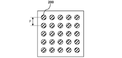
- FIG. 4 is a top view showing an example of unevenness of an adhesive layer.
- FIG. 4 is a top view showing an example of unevenness of an adhesive layer.
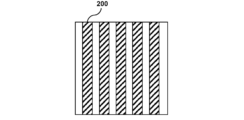
- FIG. 4 is a top view showing an example of unevenness of an adhesive layer.
- FIG. 4 is a cross-sectional view showing an example of projections and recesses on an adhesive layer.
- FIG. 4 is a cross-sectional view showing an example of projections and recesses on an adhesive layer.
- FIG. 4 is a cross-sectional view showing an example of projections and recesses on an adhesive layer.
- 1A to 1C are diagrams for explaining separation and capture of elements.
- 1A to 1C are diagrams for explaining separation and capture of elements.
- 1 is a flowchart of a manufacturing method according to an embodiment.
- 1A to 1C are diagrams illustrating a manufacturing method according to an embodiment.
- 1A to 1C are diagrams illustrating a manufacturing method according to an embodiment.
- 1A to 1C are diagrams illustrating a manufacturing method according to an embodiment.
- 1A to 1C are diagrams illustrating a manufacturing method according to an embodiment.
- FIG. 2 is a diagram for explaining an apparent contact angle.
- mass average molecular weight (Mw) and number average molecular weight (Mn) are values measured by size exclusion chromatography in terms of standard polystyrene, specifically based on JIS K7252-1:2016. It is the value to be measured.
- (meth)acrylic is a term that refers to both "acrylic” and “methacrylic”.
- electrosenor parts includes all parts used in electronic engineering, electrical engineering, etc., and all parts constituting electronic equipment.
- the “electronic component” may be formed of a semiconductor, a conductor, and/or an insulator, or a combination of these.
- Examples of “electronic components” include active components (mainly made of semiconductors, such as transistors, ICs, LSIs, VLSIs, diodes, light-emitting diodes, thyristors, three-terminal regulators, and image sensors, etc.), passive devices, etc. (e.g.
- semiconductor device refers to all devices used in processors, memories, sensors, etc., which can function by utilizing semiconductor characteristics. Examples of “semiconductor devices” include micro light emitting diodes, mini light emitting diodes, power devices, MEMS (Micro Electro Mechanical Systems), controller chips, and the like.
- any combination of the lower limit value and upper limit value among them is described.
- the description of preferably 1 or more, more preferably 2 or more, still more preferably 3 or more, preferably 9 or less, more preferably 8 or less, still more preferably 7 or less means that the numerical range is 1 or more 9 or less, 1 or more and 8 or less, 1 or more and 7 or less, 2 or more and 9 or less, 2 or more and 8 or less, 2 or more and 7 or less, 3 or more and 9 or less, 3 or more and 8 or less, and 3 or more and 7 or less. It clearly means that.
- an adhesive layer having an uneven surface is used.
- a treatment is performed on an object to be treated stuck on an adhesive layer.
- the element separated from the holding substrate may be captured on the adhesive layer in order to adhere the object to be processed on the adhesive layer.
- the adhesive layer may be provided on the base material.
- an adhesive sheet including a base material 110 and an adhesive layer 120 can be used.
- the treatment can be performed on the object stuck on the adhesive layer 120 of the adhesive sheet.
- the adhesive sheet may be composed of only the adhesive layer 120. In this case, a highly supportive adhesive layer 120 can be used.
- the substrate 110 functions as a support for the adhesive layer 120.
- the type of substrate 110 is not particularly limited, and may be a hard substrate or a flexible substrate. From the viewpoint of facilitating attachment to other members such as a substrate, improving peelability, facilitating lamination, or enabling formation into a roll form, it is preferable that the substrate 110 is a flexible substrate.
- a resin film may be used as the substrate 110.
- the resin film is a film in which a resin material is used as the main material, and may be made of the resin material, or may contain additives in addition to the resin material.
- the resin film may have laser light transmittance.
- resin films include polyethylene films such as low density polyethylene (LDPE) films, linear low density polyethylene (LLDPE) films, and high density polyethylene (HDPE) films, polypropylene films, polybutene films, polybutadiene films, and polymethyl.
- LDPE low density polyethylene
- LLDPE linear low density polyethylene
- HDPE high density polyethylene
- Polyolefin films such as pentene film, ethylene-norbornene copolymer film, and norbornene resin film; ethylene-vinyl acetate copolymer film, ethylene-(meth)acrylic acid copolymer film, and ethylene-(meth)acrylic acid film Ethylene copolymer films such as ester copolymer films; polyvinyl chloride films such as polyvinyl chloride films and vinyl chloride copolymer films; polyester films such as polyethylene terephthalate films and polybutylene terephthalate films; polyurethane films; Examples include polyimide film; polystyrene film; polycarbonate film; and fluororesin film.
- modified films such as films containing mixtures of two or more materials, crosslinked films in which the resins forming these films are crosslinked, and ionomer films may be used.
- the base material 110 may be a laminated film in which two or more types of resin films are laminated.
- the resin film may be a single-layer film selected from the group consisting of polyethylene film, polyester film, and polypropylene film. Or, it is preferable that it is a laminated film in which two or more types of films selected from this group are laminated.
- the thickness of the base material 110 is not particularly limited, but from the viewpoint of achieving both supportability and rollability, it is preferably in the range of 10 ⁇ m to 500 ⁇ m, more preferably 25 ⁇ m to 200 ⁇ m, and even more preferably 40 ⁇ m to 90 ⁇ m.
- the adhesive layer 120 is a layer having adhesiveness and can contain resin. Further, the surface of the adhesive layer 120 has irregularities. Note that the adhesive sheet may have two or more adhesive layers 120. For example, the adhesive sheet may have a laminate of one or more types of adhesive layers 120.
- composition of adhesive layer examples include rubber resins such as polyisobutylene resins, polybutadiene resins, and styrene-butadiene resins, acrylic resins, urethane resins, polyester resins, olefin resins, and silicone resins. , and polyvinyl ether resins.
- the adhesive layer may have heat resistance, and examples of materials for the adhesive layer having such heat resistance include polyimide resins and silicone resins.
- the adhesive layer may contain a copolymer having two or more types of structural units. The form of such a copolymer is not particularly limited, and may be any of a block copolymer, random copolymer, alternating copolymer, and graft copolymer.
- the resin contained in the adhesive layer 120 is an adhesive resin that has adhesive properties by itself.
- the resin is preferably a polymer having a mass average molecular weight (Mw) of 10,000 or more.
- the weight average molecular weight (Mw) of the resin is preferably 10,000 or more, more preferably 70,000 or more, and even more preferably 140,000 or more from the viewpoint of improving adhesive strength.
- it is preferably 2,000,000 or less, more preferably 1,200,000 or less, and even more preferably 900,000 or less.
- the number average molecular weight (Mn) of the resin is preferably 10,000 or more, more preferably 50,000 or more, and even more preferably 100,000 or more from the viewpoint of improving adhesive strength. Moreover, from the viewpoint of suppressing the storage elastic modulus to a predetermined value or less, it is preferably 2,000,000 or less, more preferably 1,000,000 or less, and even more preferably 700,000 or less.
- the mass average molecular weight (Mw) and number average molecular weight (Mn) are the mass average molecular weight (Mw) before crosslinking reaction due to energy application. and number average molecular weight (Mn).
- the glass transition temperature (Tg) of the resin is preferably -70°C or higher, more preferably -60°C or higher, and preferably -10°C or lower, more preferably -20°C or lower.
- Tg glass transition temperature
- the amount of resin included in the adhesive layer 120 relative to the total amount of components constituting the adhesive layer 120 can be appropriately set depending on the required adhesive strength and storage modulus of the adhesive layer 120, but is preferably 30% by mass or more. , more preferably 40% by mass or more, still more preferably 50% by mass or more, still more preferably 55% by mass or more, even more preferably 60% by mass or more, and preferably 99.99% by mass or less, more preferably 99.95% by mass. It is not more than 99.90% by mass, even more preferably not more than 99.80% by mass, even more preferably not more than 99.50% by mass.
- the resin contained in the adhesive layer 120 is preferably derived from an energy-reactive resin.
- Energy-responsive resin refers to a resin whose elastic modulus improves when energy is applied.
- Energy-reactive resins include energy-ray-reactive resins and heat-reactive resins.
- Energy ray-reactive resin refers to a resin whose elastic modulus is improved by irradiation with energy rays.
- thermalally reactive resin refers to a resin whose elastic modulus is improved by heating.
- the type of energy ray is not particularly limited, and examples thereof include ultraviolet rays, electron beams, and ionizing radiation.
- the energy beam is preferably ultraviolet rays, that is, the resin is preferably an ultraviolet-reactive resin.
- the resin is derived from an energy-responsive resin
- the resin is obtained from an energy-responsive resin.
- a resin derived from an energy-responsive resin is a crosslinked energy-responsive resin.
- the formed uneven shape can be easily maintained by applying energy (for example, irradiating with energy rays) after forming unevenness on the resin.
- the adhesive layer may contain components other than resin.
- the adhesive layer may contain one or more of a tackifier, a polymerization initiator, a UV absorber, and other additives.
- a polymerization initiator is a component that initiates a crosslinking reaction in response to application of energy (for example, irradiation with energy rays).
- energy for example, irradiation with energy rays.
- the adhesive layer contains an energy-reactive resin
- the adhesive layer further contains a polymerization initiator, so that the crosslinking reaction proceeds even when relatively low energy is applied.
- a photopolymerization initiator for example, a photopolymerization initiator can be used.
- the photopolymerization initiator include 1-hydroxycyclohexylphenyl ketone, benzoin, benzoin methyl ether, benzoin ethyl ether, benzoin propyl ether, benzylphenyl sulfide, tetramethylthiuram monosulfide, azobisisobutyronitrile, and dibenzyl. , diacetyl, and 8-chloroanthraquinone.
- the adhesive layer may contain one type of polymerization initiator, or may contain two or more types of polymerization initiator.
- the content of the polymerization initiator in the adhesive layer is preferably 0.01% by mass or more, more preferably 0.1% by mass, from the viewpoint of allowing the crosslinking reaction to proceed at an appropriate rate. It is at least 1% by mass, more preferably at least 1% by mass, preferably at most 10% by mass, more preferably at most 5% by mass, even more preferably at most 2% by mass.
- UV absorber examples include benzotriazole compounds, oxazolic acid amide compounds, and benzophenone compounds.
- additives that the adhesive layer may contain are not particularly limited, but include, for example, light stabilizers such as hindered amines, benzophenones, or benzotriazoles, phenolics such as hindered phenolic compounds, and aromatic additives.
- light stabilizers such as hindered amines, benzophenones, or benzotriazoles
- phenolics such as hindered phenolic compounds
- aromatic additives include, for example, light stabilizers such as hindered amines, benzophenones, or benzotriazoles
- phenolics such as hindered phenolic compounds
- aromatic additives aromatic additives.
- Amine-based, sulfur-based, or phosphorus-based antioxidants such as phosphate ester compounds, imidazole-based resin stabilizers, dithiocarbamate-based resin stabilizers, phosphorus-based resin stabilizers, or sulfur ester-based resin stabilizers
- resin stabilizers such as fillers, pigments, extenders,
- the content of the additives in the adhesive layer is preferably 0.0001% by mass or more, more preferably 0.01% by mass or more, particularly preferably 0.1% by mass or more, even more preferably 1% by mass or more, and is preferably 20% by mass or less, more preferably 10% by mass or less, even more preferably 5% by mass or less.
- the surface of the adhesive layer has irregularities. As will be described later, after the treatment object adhered to the adhesive layer is processed, the treatment object is removed from the adhesive layer. If the surface of the adhesive layer is flat, the adhesive layer and the object to be treated are in close contact with each other. At this time, even if you try to remove the object from the adhesive layer, it is difficult for air to enter between the adhesive layer and the object, so a sufficiently large force is required to remove the object from the adhesive layer. . On the other hand, since a gap exists between the adhesive layer having an uneven surface and the object to be treated, the object to be treated can be easily removed from the adhesive layer.
- the workpiece separated from the holding substrate can be captured by the adhesive layer.
- the adhesive layer can capture the workpiece at the convex parts.
- the gas compressed between the workpiece and the adhesive layer as the workpiece and the adhesive layer approach each other can escape to the concave parts of the adhesive layer.
- the adhesive layer has concaves and convexes, which can reduce the pressure generated between the workpiece and the adhesive layer. Therefore, it is also possible to prevent the pressure generated between the workpiece and the adhesive layer from shifting the holding position of the workpiece on the adhesive layer.
- the force required to remove the object from the adhesive layer can be adjusted by controlling the contact area between the object and the adhesive layer. Become. Moreover, if the surface of the adhesive layer has a recessed portion, the pressure generated between the object to be processed and the adhesive layer can be alleviated. Therefore, the specific shape of the unevenness on the surface of the adhesive layer is not limited.
- the adhesive layer has a plurality of protrusions on its surface that are spaced apart from each other via recesses.
- Each of the plurality of convex portions may be separated by a concave portion that is continuous throughout the adhesive layer.
- the recesses located around each of the plurality of projections are continuous to the end of the adhesive layer. In this way, by providing a concave portion that continues to the end of the adhesive layer, air can more easily enter between the object to be processed and the adhesive layer.
- FIGS. 2A to 2C are top views showing the shape of such an adhesive layer.
- convex portions may be regularly arranged on the surface of the adhesive layer.
- the convex portions being regularly arranged means that the convex portions are arranged in a straight line at regular intervals.
- the convex portions may be arranged so that the intervals vary regularly.
- the distance between the convex portions is short at the center of the adhesive layer, and the distance between the convex portions is long at the periphery of the adhesive layer. According to such a configuration, while increasing the holding power of the adhesive layer, air can easily enter between the adhesive layer and the object to be processed via the wide recess from the periphery of the object to be processed, which further reduces pressure. It can be efficiently released from the periphery of the processed material.
- the convex portions may be arranged irregularly.
- FIG. 2C is a top view showing another shape of the adhesive layer. As shown in FIG. 2C, striped convex portions may be provided on the surface of the adhesive layer. In FIG. 2C, linear convex portions having a constant width are lined up at regular intervals. On the other hand, as in FIG. 2B, the width or interval of the linear protrusions may vary regularly, or the linear protrusions may be arranged irregularly.
- the pitch of the convex portions is preferably 1 ⁇ m or more, more preferably 5 ⁇ m or more, and even more preferably 10 ⁇ m or more, from the viewpoint of facilitating the removal of the object to be treated or enhancing the pressure relief effect. More preferably, it is 15 ⁇ m or more.
- the pitch of the convex parts means the minimum interval among all the intervals of the convex parts in the entire adhesive layer.
- the pitch of the convex portions represents the interval between the convex portions on a straight line in which the convex portions are arranged at regular intervals.
- the pitch represents the interval between the protrusions on the straight line in which the protrusions are lined up at the shortest interval. Further, in the case of FIG. 2C, the pitch of the convex portions represents the interval between the linear convex portions.
- the distance between the convex portions means the distance between the centers of the convex portions.
- the contact area between the adhesive layer and the object to be processed can be increased, suppressing misalignment during capture.
- the object to be processed on the adhesive is sealed with a sealant.
- the wettability of the sealant to the surface of the adhesive layer before hardening is reduced, and the sealant is less likely to penetrate into the unevenness. This phenomenon of reduced wettability on a surface with a fine structure is generally called the lotus effect.
- the pitch of the protrusions is preferably 100 ⁇ m or less, more preferably 75 ⁇ m or less, even more preferably 50 ⁇ m or less, even more preferably 35 ⁇ m or less, and even more preferably 25 ⁇ m or less.
- the minimum spacing among all the protrusion spacings in the center of the adhesive layer may be shorter than the minimum spacing among all the protrusion spacings in the peripheral portion of the adhesive layer.
- the center is, for example, a circular region having 1/4 of the area of the adhesive layer and centered on the center of gravity of the adhesive layer
- the peripheral portion is, for example, the entire area of the adhesive layer other than the center.
- the convex portion may have a pillar shape.
- the convex portion may have a cylindrical shape or a prismatic shape.
- the convex portion may extend in a line shape, or may extend in a curved shape such as a wave shape.
- these convex portions may be provided with a taper.
- FIG. 3A shows a cross-sectional view of the adhesive layer according to one embodiment, passing through the convex portion and perpendicular to the surface of the adhesive layer.
- the convex portion shown in FIG. 3A is tapered, that is, the convex portion is tapered.
- the tip of the convex portion may be a curved surface. With this configuration, the impact when the adhesive layer comes into contact with the workpiece separated from the holding substrate is more relaxed, so the adhesive layer can easily hold the workpiece so that it does not shift. become. On the other hand, the tip of the convex portion may be flat.
- the surface of the adhesive layer may have flat recesses and protrusions protruding from the recesses.
- the plurality of convex portions that the adhesive layer has and are spaced apart from each other may be bounded by concave portions.
- the convex portion may be hemispherical or part of a sphere, as shown in FIG. 3B. Further, the convex portion may be T-shaped as shown in FIG. 3C. As yet another example, the convex portion may have a shape in which a plurality of grains are gathered together, a mushroom shape, a surface shape of a lotus leaf, or a needle shape. As yet another example, the surface of the adhesive layer may be rough or fibrous, and such a surface can also be said to have irregularities.
- each convex portion is preferably 1 ⁇ m or more, more preferably 2 ⁇ m or more, even more preferably 5 ⁇ m or more, and preferably 10 ⁇ m or more from the viewpoint of maintaining adhesiveness. More preferred.
- the width or diameter of each convex portion is preferably 100 ⁇ m or less, more preferably 50 ⁇ m or less, and 30 ⁇ m or less, from the viewpoint of facilitating the removal of the object to be treated or enhancing the pressure relief effect. It is more preferable that it is, and it is even more preferable that it is 20 ⁇ m or less.
- the width and diameter of the convex portion respectively mean the minimum distance and maximum distance (represented by B in FIG. 3A) between two parallel lines touching from both sides of the convex portion on the surface of the concave portion.
- the area of each convex portion is preferably 10 ⁇ m 2 or more, more preferably 20 ⁇ m 2 or more, and even more preferably 30 ⁇ m 2 or more.
- the area of each convex portion is preferably 2000 ⁇ m 2 or less, more preferably 1000 ⁇ m 2 or less, and 500 ⁇ m 2 from the viewpoint of facilitating the removal of the object to be treated or enhancing the pressure relief effect. It is more preferable that it is the following.
- the area of the convex portion means the area of the portion protruding from the surface of the concave portion (in the case of FIG. 3A, the area of a circle with diameter B).
- each convex portion is preferably 1 ⁇ m or more, more preferably 3 ⁇ m or more, and even more preferably 5 ⁇ m or more, from the viewpoint of making it easier for air to enter the recess.
- the height of each convex portion is preferably 20 ⁇ m or less, more preferably 15 ⁇ m or less, and even more preferably 10 ⁇ m or less.
- the height of the convex portion is represented by H in FIG. 3A.
- the area occupied by the plurality of convex portions relative to the area of the adhesive layer is preferably 1% or more, more preferably 5% or more, and 10% or more. is more preferable, more preferably 18% or more, even more preferably 40% or more.
- the area of each convex portion is preferably 95% or less, more preferably 75% or less, and even more preferably 60% or less.
- the unevenness of the adhesive layer may be designed according to the shape of the object to be processed.
- the ratio of the adhesion area between the adhesive layer and one workpiece to the area of one workpiece is preferably 1% or more, and preferably 2% or more. is more preferably 3% or more, even more preferably 4% or more, even more preferably 5% or more, even more preferably 7% or more, and even more preferably 10% or more. is even more preferable.
- the area of each convex portion is preferably 95% or less, more preferably 70% or less, and 50% It is more preferably at most 30%, even more preferably at most 30%. In the case of FIG.
- the adhesive area corresponds to the area of a circle with diameter T. Note that if the position of the object to be processed on the adhesive layer shifts, the adhesive area may change. In this case, it is preferable that the bonding area ratio falls within the above range regardless of the position of the object to be treated.
- the above adhesive sheet may have layers other than the base material 110 and the adhesive layer 120.
- an additional adhesive layer may be provided on the surface of the base material 110 opposite to the adhesive layer 120.
- the adhesive sheet can be attached to another substrate such as quartz glass through such an adhesive layer.
- the type of the additional adhesive layer is not particularly limited, and for example, the additional adhesive layer can be formed using a common adhesive.
- an adhesive sheet in which the adhesive layer 120 is provided on the base material 110 can be produced as follows. First, an organic solvent is added to a raw material composition containing each component of the adhesive layer described above to prepare a solution of the raw material composition. Then, an adhesive layer can be provided on the base material 110 by applying this solution onto the base material to form a coating film and then drying it. Furthermore, by performing a process to provide unevenness on the surface of this adhesive layer, it is possible to form an adhesive layer 120 having unevenness.
- Examples of the organic solvent used to prepare the solution of the raw material composition include toluene, ethyl acetate, and methyl ethyl ketone.
- the solid content concentration of the solution of the raw material composition is preferably 10% by mass or more, more preferably 25% by mass or more, even more preferably 45% by mass or more, and preferably 80% by mass or less, more preferably 70% by mass or less. , more preferably 65% by mass or less.
- Examples of methods for applying the solution include spin coating, spray coating, bar coating, knife coating, roll coating, roll knife coating, blade coating, die coating, gravure coating, and printing (e.g. screen printing method, inkjet method), etc.
- unevenness can be provided on the surface of the adhesive layer using an imprint method.
- a mold having a surface complementary to the unevenness to be provided can be used.
- unevenness can be provided on the surface of the adhesive layer by heating the adhesive layer while pressing the adhesive layer provided on the base material with a mold.
- the adhesive layer is pressed with a mold, the adhesive layer is heated and maintained for a predetermined period of time, and then the adhesive layer is cooled and the mold can be removed.
- the adhesive layer can be heated to a temperature higher than the softening point of the adhesive layer, for example.
- the time period for maintaining the adhesive layer in the heated state is not particularly limited, but may be maintained for 10 seconds or more, or for 10 minutes or less, for example.
- a specific method for heating the adhesive layer while pressing it with a mold includes a method of vacuum laminating the adhesive layer provided on the base material and the mold. Note that instead of performing the two-step process of forming an adhesive layer and forming unevenness, the adhesive layer 120 having an uneven surface may be formed on the base material 110 in a one-step process.
- an adhesive layer having a rough surface can be provided by spray coating a solution of the raw material composition. Furthermore, an adhesive layer having a rough or fibrous surface can be provided by adding a filler to a solution of the raw material composition and applying such a solution. As yet another method, an adhesive layer having an uneven shape can be directly provided on a substrate by applying a solution of the raw material composition according to a desired pattern using a printing method such as an inkjet method.
- an adhesive sheet without the base material 110 can be produced by forming a composition containing each component of the adhesive layer into a sheet shape.
- the adhesive layer may be formed by applying a liquid adhesive containing each component of the adhesive layer to an arbitrary object.
- a treatment may be performed to provide unevenness on the surface of the adhesive layer, or the adhesive layer may be formed by a method in which unevenness is formed on the surface.
- step S10 a workpiece used for manufacturing an electronic component or a semiconductor device is adhered to the uneven surface of the adhesive layer.
- an object to be processed 520 can be attached to the surface of an adhesive sheet 510.
- the object to be processed can be placed on the adhesive layer using a device such as a flip chip bonder or a die bonder.
- the arrangement layout and number of objects to be processed can be determined as appropriate depending on the form of the sealed body to be produced, the number of products to be produced, and the like.
- the type of object to be processed is not particularly limited.
- the object to be processed may be, for example, an element, a wafer, a panel, or a substrate.
- the element may be, for example, a semiconductor chip such as an LED chip, a semiconductor chip with a protective film, a semiconductor chip with a die attach film (DAF), or the like.
- the element may be a micro light emitting diode, a mini light emitting diode, a power device, MEMS (Micro Electro Mechanical Systems), or a controller chip, or a component thereof.
- the element may be a wafer, a panel, a substrate, or the like.
- the device may, for example, have a circuit surface on which an integrated circuit is formed having circuit elements such as transistors, resistors, and capacitors.
- the size of the element is not particularly limited.
- the size of the element may be, for example, 100 ⁇ m 2 or more, 500 ⁇ m 2 or more, or 1000 ⁇ m 2 or more.
- the size of the element may be 100 mm 2 or less, 25 mm 2 or less, or 1 mm 2 or less.
- the laser lift-off method described later is suitable for bonding the elements because it is easy to selectively separate small elements.
- the object to be processed is not necessarily limited to singulated objects.
- the object to be processed may be various wafers, various panels, or various substrates that are not separated into pieces.
- wafers examples include silicon wafers, silicon carbide (SiC) wafers, compound semiconductor wafers (e.g., gallium phosphide (GaP) wafers, gallium arsenide (GaAs) wafers, indium phosphide (InP) wafers, gallium nitride (GaN)).
- semiconductor wafers such as wafers.
- the size of the wafer is not particularly limited, but may be 8 inches (diameter 200 mm) or more, preferably 12 inches (diameter 300 mm) or more. Note that the shape of the wafer is not limited to a circle, and may be square or rectangular, for example.
- the panel examples include fan-out semiconductor packages (for example, FOWLP or FOPLP). That is, the object to be processed may be a semiconductor package before or after singulation in a fan-out type semiconductor package manufacturing technique.
- the size of the panel is not particularly limited, it may be a rectangular substrate of about 300 to 700 mm, for example.
- the substrate examples include a glass substrate, a sapphire substrate, a compound semiconductor substrate, and the like.
- the element When using an adhesive layer having an uneven surface, it is preferable to transfer the element from the holding substrate to the adhesive layer by a method including the steps of separating the element from the holding substrate and capturing the element in the adhesive layer. . In this way, the element can be attached to the uneven surface of the adhesive layer. Such a method will be explained below.
- a holding substrate to which an element is attached is prepared.
- the type of holding substrate is also not particularly limited.
- the holding substrate may be an adhesive sheet or a tray.
- the adhesive sheet may have an adhesive layer, and this adhesive layer may be provided on the base material.
- the holding substrate can hold the element on the adhesive layer.
- the base material may be a resin film or a hard substrate.
- the method of preparing such a holding substrate that holds the element is not particularly limited either.
- a semiconductor wafer can be attached onto a holding substrate, and then the semiconductor wafer can be diced. By dicing the semiconductor wafer in this manner, elements can be obtained, and therefore a holding substrate to which the elements are attached can be obtained.
- the holding substrate As another method, by transferring the elements obtained by dicing the semiconductor wafer onto the holding substrate, it is possible to obtain the holding substrate to which the elements are attached. For example, after dicing a semiconductor wafer held on a wafer substrate, the obtained elements can be brought into close contact with the adhesive layer of the holding substrate. Thereafter, by applying an external stimulus such as a laser beam, the adhesiveness between the wafer substrate and the element can be reduced. Through such a process, the elements can be transferred from the wafer substrate to the holding substrate.
- an external stimulus such as a laser beam
- the element can be separated from the holding substrate by laser light irradiation (laser lift-off method).
- the adhesive layer of the holding substrate preferably contains a laser light absorber.
- the laser light absorbent include one or more selected from pigments and dyes.
- the element attached to the holding substrate is separated from the holding substrate by external stimulation.
- the type of external stimulus is not particularly limited, and examples thereof include energy application, cooling, stretching of the holding substrate, and physical stimulation (for example, pressing the back surface of the holding substrate with a pin or the like).
- the elements can be captured such that the relative arrangement of the plurality of elements on the holding substrate is different from the relative arrangement of the plurality of elements on the adhesive layer.
- Examples of energy imparting methods include local heating, light irradiation, and heat ray irradiation.
- Examples of the light irradiation method include infrared irradiation, visible light irradiation, and laser light irradiation.
- laser light irradiation is used as the external stimulus, that is, separation of the element from the holding substrate is performed by a laser lift-off method.
- the laser beam is irradiated toward a part of the holding substrate where a specific element is attached.
- such laser light irradiation can be performed from the surface of the holding substrate opposite to the element. Then, gas is generated at the contact site between the specific element and the holding substrate.
- the adhesive layer when laser light is absorbed by the adhesive layer, at least a portion of the adhesive layer sublimates, thereby generating gas.
- the adhesive area between a specific element and the adhesive layer decreases, and thus the adhesive force between the specific element and the holding substrate decreases.
- the pressure of the generated gas also reduces the adhesive force between a specific element and the holding substrate. As a result, certain elements are separated from the holding substrate.
- the laser light irradiation conditions are not particularly limited. From the viewpoint of selectively and efficiently separating some elements, the frequency of the laser beam is preferably 10,000 Hz or more and 100,000 Hz or less. Further, the beam diameter of the laser beam is preferably 10 ⁇ m or more, more preferably 20 ⁇ m or more, and preferably 100 ⁇ m or less, more preferably 40 ⁇ m or less. The output of the laser beam is preferably 0.1 W or more and 10 W or less. The scanning speed of the laser beam is preferably 50 mm/sec or more and 2000 mm/sec or less.
- the separated element 420 is placed at the position A on the adhesive sheet 450. captured at Furthermore, as shown in FIG. 4B, by positioning position B on the adhesive sheet 450 so as to face the element 430 attached to the holding substrate 410, the separated element 430 is placed on the adhesive sheet 450. Captured at position B. In this way, elements can be separated and captured while changing the relative position of the holding substrate and the adhesive layer in the plane direction. In this way, the elements can be positioned so that the relative arrangement of the plurality of elements on the holding substrate is different from the relative arrangement of the plurality of elements on the adhesive layer.
- the element 420 when using an adhesive layer with a flat surface, the element 420 is captured at a position shifted from position A in the example of FIG. 4A due to the pressure generated between the element and the adhesive layer. It might happen. However, since the surface of the adhesive layer has irregularities, the pressure generated between the element and the adhesive layer is alleviated, so that it becomes easier to capture the element at a desired position on the adhesive layer.
- the holding substrate and the adhesive layer are stationary, and the device separated from the holding substrate moves to the adhesive layer.
- the element can be moved toward the adhesive layer due to gas pressure generated by laser light irradiation.
- the holding substrate may be moved away from the element.
- the adhesive layer may be moved closer to the element.
- step S20 the object to be processed on the adhesive layer is processed.
- the processing method is not particularly limited. For example, processes such as wiring formation, back metal formation, cleaning, plating, singulation, and thinning can be performed.
- the processing for the object to be processed includes energy imparting processing (e.g., heating or irradiation with energy rays such as light), liquid contact processing (e.g., etching), vacuum processing (e.g., vacuum evaporation or sputtering), or sealing processing. It's okay to stay. Through such processing, a processed product can be obtained. Below, as an example, a case where an element is sealed will be described.
- a sealed body is formed by sealing the element on the adhesive layer with a sealing material.
- the element stuck on the adhesive layer is covered with a sealant.
- the element 520 is covered with a sealing material 530 so that the exposed surface of the element 520, for example, the surface and side surface of the element 520 opposite to the adhesive sheet 510 are covered. Can be coated.
- the sealing material 530 when covering the element 520 with the sealing material 530, the surface of the element 520 on the adhesive sheet 510 side does not need to be covered.
- two or more elements 520 may be integrally covered with the sealing material 530. In the example of FIG. 6B, two or more elements 520 spaced apart on the uneven surface are sealed together.
- the gap between two or more elements 520 is filled with encapsulant 530.
- the sealant is then cured.
- a sealed body 550 including the element 520 is formed as shown in FIG. 6C.
- the sealing body 550 can be formed such that the sealing material contacts both the element and the uneven surface of the adhesive layer.
- the sealing body 550 can be formed so that the recesses on the surface of the adhesive sheet 510 are not filled with the sealant 530 and air enters the recesses.
- the apparent contact angle between the uneven surface of the adhesive layer and the sealing material before curing (the contact angle when the uneven surface is regarded as a flat surface) is determined. , represented by ⁇ in FIG. 7) preferably exceeds 90°, more preferably exceeds 100°, and even more preferably exceeds 110°.
- the contact angle between this layer and the sealing material before curing is preferably over 90°, more preferably over 100°, and 110°.
- the adhesive is selected so that the temperature exceeds .
- the apparent contact angle between the uneven surface of the adhesive layer and the uncured encapsulant is larger than the contact angle between this layer and the uncured encapsulant when a flat layer of the adhesive is formed. It has become.
- the sealing material has the function of protecting the element and its accompanying elements from the external environment. There are no particular restrictions on the type of sealant.
- the sealing material has curability from the viewpoints of mechanical strength, heat resistance, insulation, and the like.
- the sealing material examples include thermosetting resin compositions and energy ray curable resin compositions.
- the thermosetting resin contained in the thermosetting resin composition include epoxy resins, phenol resins, and cyanate resins. From the viewpoints of mechanical strength, heat resistance, insulation, moldability, etc., the thermosetting resin is preferably an epoxy resin.
- the thermosetting resin composition may optionally contain a curing agent such as a phenol resin curing agent or an amine curing agent, a curing accelerator, an inorganic filler such as silica, or an elastomer. It may contain additives such as.
- the sealing material may be solid or liquid at room temperature. Further, the form of the sealing material that is solid at room temperature is not particularly limited, and may be, for example, in the form of granules or sheets.
- the method of covering the element with the sealing material is not particularly limited, but for example, a roll lamination method, a vacuum press method, a vacuum lamination method, a spin coating method, a die coating method, a transfer molding method, a compression molding method, etc. may be applied. Can be done. In these methods, in order to improve the filling properties of the sealant, the sealant can be heated during coating to impart fluidity.
- a sealed body having a desired shape can be obtained by filling a sealing material into a cavity having a desired shape and pressing the mold.
- a cavity within the mold 540 is filled with a sealing material 530.
- the molding pressure at this time is, for example, 0.1 MPa or more, preferably 0.2 MPa or more, more preferably 0.3 MPa or more, and, for example, 2.0 MPa or less, preferably 1.8 MPa or less, more preferably 1.6 MPa or less. It is.
- compression molding may be performed while reducing the pressure inside the cavity.
- the sealing material can be cured during pressurization.
- the sealant can be cured by heating the sealant.
- the heating temperature at this time can be selected depending on the type of sealing material, but is, for example, 30°C or higher, preferably 50°C or higher, more preferably 70°C or higher, and, for example, 180°C or lower, preferably 170°C.
- the temperature below is more preferably 150°C or below.
- the heating time is, for example, 5 seconds or more, preferably 10 seconds or more, more preferably 15 seconds or more, and is, for example, 60 minutes or less, preferably 45 minutes or less, more preferably 30 minutes or less.
- two or more objects to be processed that are placed apart on the uneven surface can be integrally sealed. Furthermore, after two or more objects to be processed are integrally sealed, they may be further separated into pieces. For example, by integrally sealing an assembly of packages containing two or more objects to be processed, and then dividing the assembly into individual pieces, a plurality of packages each containing an object to be processed are produced. be able to.
- a rewiring layer can be formed on the surface of the sealing body. That is, the method for manufacturing an electronic component or a semiconductor device according to the present embodiment can be used in a fan-out type process such as FOWLP or FOPLP. For example, a region larger than the element size can be covered with the sealing material, and furthermore, a rewiring layer and external electrodes can be formed not only on the circuit surface of the element but also on the surface of the sealing material.
- the above treatments for objects to be treated can also be used in combination. For example, after two or more objects to be processed are integrally sealed and a rewiring layer is formed on the surface of the sealing material, the resulting structure may be separated into pieces.
- step S30 the processing resultant obtained by processing the object to be processed is removed from the adhesive layer.
- the sealing body 550 is removed from the adhesive sheet 510, as shown in FIG. 6D.
- the sealing body 550 since air is contained in the recesses on the surface of the adhesive sheet 510, the sealing body 550 is adhered to the adhesive sheet 510, but the sealing body 550 is not in close contact with the adhesive sheet 510. It has no parts. Therefore, the sealing body 550 can be easily removed from the adhesive sheet 510 compared to the case where the adhesive layer has no unevenness.
- a reinforcing member may be attached to the surface opposite to the surface where the reinforcing member is attached.
- the reinforcing member is not particularly limited, for example, a reinforcing plate having excellent heat resistance such as glass epoxy resin can be used. Such a reinforcing plate can be attached to the entire surface of the sealed body.
- the reinforcing member can be attached via an adhesive layer, for example. Since the reinforcing element is removed after further processing, it is preferable to select an adhesive layer that allows the reinforcing element to be peeled off.
- Such a reinforcing member can be attached, for example, by laminating a thermosetting adhesive layer and a reinforcing plate on the sealing body in this order. Furthermore, if necessary, both the reinforcing plate side and the adhesive layer side may be sandwiched between plate-like members and pressed under conditions of predetermined temperature, time, and pressure.
- a metal plate such as stainless steel can be used.
Landscapes
- Engineering & Computer Science (AREA)
- Physics & Mathematics (AREA)
- Condensed Matter Physics & Semiconductors (AREA)
- General Physics & Mathematics (AREA)
- Manufacturing & Machinery (AREA)
- Computer Hardware Design (AREA)
- Microelectronics & Electronic Packaging (AREA)
- Power Engineering (AREA)
- Chemical & Material Sciences (AREA)
- Organic Chemistry (AREA)
- Adhesives Or Adhesive Processes (AREA)
Abstract
電子部品又は半導体装置を製造する際に、処理後の素子の取り外しを容易として生産性を高めるための新たな方法を提供する。 粘着層が有する凹凸表面に、電子部品又は半導体装置を製造するために用いられる被処理物を貼着する。粘着層上の前記被処理物に対する処理を行うことにより、処理結果物を得る。処理結果物を前記粘着層から取り外す。
Description
本発明は、電子部品又は半導体装置の製造方法に関し、例えば半導体素子を封止する技術に関する。
電子部品又は半導体装置の製造においては、例えば特許文献1に記載されているように、素子の封止又は配線などの、被処理物に対する処理が行われる。被処理物に対する処理は、特許文献1に記載されているように、被処理物が粘着シートに貼着されている状態で行われることが多い。
被処理物に対する処理を行った後には、処理結果物を粘着シートから取り外す必要がある。しかしながら、処理結果物を容易に粘着シートから取り外せるようにすることは容易ではなかった。特許文献1は、素子の取り外しを容易として生産性を高めるために、粘着剤に熱膨張性粒子を添加することを提案している。
本発明は、電子部品又は半導体装置を製造する際に、処理結果物の取り外しを容易として生産性を高めるための新たな方法を提供することを目的とする。
本発明者は、鋭意検討を重ねた結果、粘着層が有する凹凸表面に被処理物を貼着してから被処理物に対する処理を行うことにより、処理結果物の取り外しを容易として生産性を高めることができ、こうして上記課題を解決できることを見出し、更に種々検討を重ね、本発明を完成するに至った。
すなわち、本発明は、下記[1]~[13]に関する。
[1]粘着層が有する凹凸表面に、電子部品又は半導体装置を製造するために用いられる被処理物を貼着する工程と、
前記粘着層上の前記被処理物に対する処理を行うことにより、処理結果物を得る工程と、
前記処理結果物を前記粘着層から取り外す工程と、
を含む、電子部品又は半導体装置の製造方法。
[2]前記被処理物は、素子、半導体ウエハ、又はパネルである、[1]に記載の製造方法。
[3]前記被処理物に対する処理は、エネルギー付与処理、液体接触処理、真空下処理、又は封止処理を含む、[1]に記載の製造方法。
[4]前記処理を行う工程では、前記粘着層上の前記被処理物を封止材で封止することにより封止体を形成し、
前記取り外す工程では、前記被処理物を含む前記封止体を前記粘着層から取り外す、[1]に記載の製造方法。
[5]前記処理を行う工程では、前記封止材が前記被処理物と前記粘着層が有する凹凸表面の双方に接触するように前記封止体を形成する、[4]に記載の製造方法。
[6]前記処理を行う工程では、前記凹凸表面上に離れて配置された2つ以上の前記被処理物を一体的に封止する、[4]に記載の製造方法。
[7]前記処理を行う工程では、2つ以上の前記被処理物を一体的に封止した後に、さらに個片化を行う、[6]に記載の製造方法。
[8]前記被処理物を貼着する工程が、保持基板から分離させた被処理物を前記粘着層において捕捉する工程を含む、[1]に記載の製造方法。
[9]前記粘着層は、基材と、前記基材上に形成され、表面が凹凸を有する粘着層と、を備える、[1]に記載の製造方法。
[10]前記粘着層は、前記表面に、凹部を介して互いに離間している複数の凸部を有する、[1]から[9]のいずれかに記載の製造方法。
[11]前記粘着層は、凹部によって境界が定められる凸部を有し、
前記粘着層の面積に対する、前記凸部が占める面積の比が、1%以上、95%以下である、[1]から[9]のいずれかに記載の製造方法。
[12]1つの前記被処理物の面積に対する、前記粘着層と1つの前記被処理物との接着面積の比が、1%以上、95%以下となるように前記粘着層が構成されている、[1]から[9]のいずれかに記載の製造方法。
[13]前記被処理物の面積が100mm2以下である、[1]から[9]のいずれかに記載の製造方法。
電子部品又は半導体装置を製造する際に、処理結果物の取り外しを容易として生産性を高めるための新たな方法を提供することができる。
本発明のその他の特徴及び利点は、添付図面を参照とした以下の説明により明らかになるであろう。なお、添付図面においては、同じ若しくは同様の構成には、同じ参照番号を付す。
添付図面は明細書に含まれ、その一部を構成し、本発明の実施の形態を示し、その記述と共に本発明の原理を説明するために用いられる。
一実施形態に係る粘着シートの模式図。
粘着層が有する凹凸の一例を示す上面図。
粘着層が有する凹凸の一例を示す上面図。
粘着層が有する凹凸の一例を示す上面図。
粘着層が有する凹凸の一例を示す断面図。
粘着層が有する凹凸の一例を示す断面図。
粘着層が有する凹凸の一例を示す断面図。
素子の分離及び捕捉について説明する図。
素子の分離及び捕捉について説明する図。
一実施形態に係る製造方法のフローチャート。
一実施形態に係る製造方法について説明する図。
一実施形態に係る製造方法について説明する図。
一実施形態に係る製造方法について説明する図。
一実施形態に係る製造方法について説明する図。
見かけの接触角について説明する図。
以下、添付図面を参照して実施形態を詳しく説明する。なお、以下の実施形態は特許請求の範囲に係る発明を限定するものではなく、また実施形態で説明されている特徴の組み合わせの全てが発明に必須のものとは限らない。実施形態で説明されている複数の特徴のうち二つ以上の特徴は任意に組み合わされてもよい。また、同一若しくは同様の構成には同一の参照番号を付し、重複した説明は省略する。
(定義)
本明細書において、質量平均分子量(Mw)及び数平均分子量(Mn)は、サイズ排除クロマトグラフィー法で測定される標準ポリスチレン換算の値であり、具体的にはJIS K7252-1:2016に基づいて測定される値である。また、本明細書において、「(メタ)アクリル」は、「アクリル」と「メタクリル」の双方を指す用語である。
本明細書において、質量平均分子量(Mw)及び数平均分子量(Mn)は、サイズ排除クロマトグラフィー法で測定される標準ポリスチレン換算の値であり、具体的にはJIS K7252-1:2016に基づいて測定される値である。また、本明細書において、「(メタ)アクリル」は、「アクリル」と「メタクリル」の双方を指す用語である。
本明細書において、「電子部品」とは、電子工学及び電気工学等において使用される全ての部品、並びに電子機器を構成する全ての部品を包含するものである。「電子部品」は、半導体、導電体及び/又は絶縁体のいずれかによって、あるいはこれらが組み合わせられて形成されていてもよい。「電子部品」としては、例えば、能動部品(主に半導体から形成され、例えば、トランジスタ、IC、LSI、超LSI、ダイオード、発光ダイオード、サイリスタ、三端子レキュレータ、及び撮像素子、等)、受動素子(例えば、抵抗器、コンデンサ、スピーカ、コイル、変圧器、変成器、リレー、圧電素子、水晶振動子、セラミック発振子、及びバリスタ等)、並びに構造部品(例えば、配線部品、プリント基板、コネクタ、及び開閉器等)等が挙げられる。また、本明細書において「半導体装置」とは、プロセッサ、メモリ、及びセンサ等に用いられる、半導体特性を利用することで機能し得る装置全般のことを指す。「半導体装置」の例としては、マイクロ発光ダイオード、ミニ発光ダイオード、パワーデバイス、MEMS(Micro Electro Mechanical Systems)、及びコントローラチップなどが挙げられる。
本明細書において、数値範囲(例えば含有量等の範囲)の1以上の下限値及び1以上の上限値が記載されている場合、その中の任意の下限値と上限値と組み合わせが記載されているものと理解できる。例えば、好ましくは1以上、より好ましくは2以上、さらに好ましくは3以上であり、好ましくは9以下、より好ましくは8以下、さらに好ましくは7以下であるとの記載は、数値範囲が、1以上9以下、1以上8以下、1以上7以下、2以上9以下、2以上8以下、2以上7以下、3以上9以下、3以上8以下、及び3以上7以下のいずれであってもよいことを明確に意味する。
本発明の一実施形態に係る電子部品又は半導体装置の製造方法においては、凹凸表面を有する粘着層が用いられる。例えば、この製造方法においては、粘着層上に貼着された被処理物に対して処理が行われる。また、後述するように、粘着層に被処理物を貼着するために、粘着層において保持基板から分離させた素子を捕捉してもよい。本明細書では、まず、この電子部品又は半導体装置の製造方法において用いられる、凹凸表面を有する粘着層について説明する。
(基材)
粘着層は、基材上に設けられていてもよい。例えば、図1に示すように、基材110と粘着層120とを備える粘着シートを用いることができる。この場合、粘着シートの粘着層120上に貼着された被処理物に対して処理を行うことができる。もっとも、粘着シートが基材110を有することは必須ではない。例えば、粘着シートは粘着層120のみで構成されていてもよい。この場合には支持性の高い粘着層120を用いることができる。
粘着層は、基材上に設けられていてもよい。例えば、図1に示すように、基材110と粘着層120とを備える粘着シートを用いることができる。この場合、粘着シートの粘着層120上に貼着された被処理物に対して処理を行うことができる。もっとも、粘着シートが基材110を有することは必須ではない。例えば、粘着シートは粘着層120のみで構成されていてもよい。この場合には支持性の高い粘着層120を用いることができる。
基材110は、粘着層120を支持する支持体として機能する。基材110の種類は特に限定されず、硬質基材又はフレキシブル基材でありうる。基板等の他の部材への取り付けを容易とする、剥離性を向上させる、積層を容易とする、又はロール形態とすることを可能にする観点から、基材110はフレキシブル基材であることが好ましい。基材110としては、例えば樹脂フィルムを用いることができる。
樹脂フィルムは、主材として樹脂系の材料が用いられているフィルムであり、樹脂材料からなっていてもよいし、樹脂材料に加えて添加剤を含んでいてもよい。樹脂フィルムは、レーザ光透過性を有していてもよい。
樹脂フィルムの具体例としては、低密度ポリエチレン(LDPE)フィルム、直鎖低密度ポリエチレン(LLDPE)フィルム、及び高密度ポリエチレン(HDPE)フィルム等のポリエチレンフィルム、ポリプロピレンフィルム、ポリブテンフィルム、ポリブタジエンフィルム、ポリメチルペンテンフィルム、エチレン-ノルボルネン共重合体フィルム、並びにノルボルネン樹脂フィルム等のポリオレフィン系フィルム;エチレン-酢酸ビニル共重合体フィルム、エチレン-(メタ)アクリル酸共重合体フィルム、及びエチレン-(メタ)アクリル酸エステル共重合体フィルム等のエチレン系共重合体系フィルム;ポリ塩化ビニルフィルム及び塩化ビニル共重合体フィルム等のポリ塩化ビニル系フィルム;ポリエチレンテレフタレートフィルム及びポリブチレンテレフタレートフィルム等のポリエステル系フィルム;ポリウレタンフィルム;ポリイミドフィルム;ポリスチレンフィルム;ポリカーボネートフィルム;並びにフッ素樹脂フィルム等が挙げられる。また、2種類以上の材料の混合物を含むフィルム、のこれらのフィルムを形成する樹脂が架橋されている架橋フィルム、及びアイオノマーフィルムのような変性フィルムを用いてもよい。また、基材110は、2種類以上の樹脂フィルムが積層された積層フィルムであってもよい。
汎用性の観点、強度が比較的高く反りを防止しやすい観点、及び耐熱性の観点から、樹脂フィルムとしては、ポリエチレンフィルム、ポリエステル系フィルム、並びにポリプロピレンフィルムからなる群から選択される単層フィルム、又はこの群から選択される2種類以上のフィルムが積層された積層フィルムであることが好ましい。
基材110の厚さは、特に限定されないが、支持性とロール巻回性の両立の観点から、好ましくは10μm~500μm、より好ましくは25μm~200μm、さらに好ましくは40μm~90μmの範囲である。
(粘着層)
粘着層120は、粘着性を有する層であり、樹脂を含むことができる。また、粘着層120の表面は凹凸を有している。なお、粘着シートは、2層以上の粘着層120を有していてもよい。例えば、粘着シートは、1種類又は2種類以上の粘着層120の積層体を有していてもよい。
粘着層120は、粘着性を有する層であり、樹脂を含むことができる。また、粘着層120の表面は凹凸を有している。なお、粘着シートは、2層以上の粘着層120を有していてもよい。例えば、粘着シートは、1種類又は2種類以上の粘着層120の積層体を有していてもよい。
(粘着層の組成)
粘着層が含む樹脂の例としては、ポリイソブチレン系樹脂、ポリブタジエン系樹脂、及びスチレン・ブタジエン系樹脂等のゴム系樹脂、アクリル系樹脂、ウレタン系樹脂、ポリエステル系樹脂、オレフィン系樹脂、シリコーン系樹脂、及びポリビニルエーテル系樹脂等が挙げられる。粘着層は耐熱性を有していてもよく、このような耐熱性を有する粘着層の材料としては、ポリイミド系樹脂及びシリコーン系樹脂が挙げられる。粘着層は、2種類以上の構成単位を有する共重合体を含んでいてもよい。このような共重合体の形態は特に限定されず、ブロック共重合体、ランダム共重合体、交互共重合体、及びグラフト共重合体のいずれであってもよい。
粘着層が含む樹脂の例としては、ポリイソブチレン系樹脂、ポリブタジエン系樹脂、及びスチレン・ブタジエン系樹脂等のゴム系樹脂、アクリル系樹脂、ウレタン系樹脂、ポリエステル系樹脂、オレフィン系樹脂、シリコーン系樹脂、及びポリビニルエーテル系樹脂等が挙げられる。粘着層は耐熱性を有していてもよく、このような耐熱性を有する粘着層の材料としては、ポリイミド系樹脂及びシリコーン系樹脂が挙げられる。粘着層は、2種類以上の構成単位を有する共重合体を含んでいてもよい。このような共重合体の形態は特に限定されず、ブロック共重合体、ランダム共重合体、交互共重合体、及びグラフト共重合体のいずれであってもよい。
粘着層120が含む樹脂は、単独で粘着性を有する粘着性樹脂であることが好ましい。また、樹脂は、1万以上の質量平均分子量(Mw)を有する重合体であることが好ましい。樹脂の質量平均分子量(Mw)は、粘着力の向上の観点から、好ましくは1万以上、より好ましくは7万以上、さらに好ましくは14万以上である。また、貯蔵弾性率を所定値以下に抑える観点から、好ましくは200万以下、より好ましくは120万以下、さらに好ましくは90万以下である。また、樹脂の数平均分子量(Mn)は、粘着力の向上の観点から、好ましくは1万以上、より好ましくは5万以上、さらに好ましくは10万以上である。また、貯蔵弾性率を所定値以下に抑える観点から、好ましくは200万以下、より好ましくは100万以下、さらに好ましくは70万以下である。なお、後述するように粘着層120がエネルギー反応性樹脂に由来する樹脂を含む場合、この質量平均分子量(Mw)及び数平均分子量(Mn)はエネルギー付与による架橋反応前の質量平均分子量(Mw)及び数平均分子量(Mn)を指す。また、樹脂のガラス転移温度(Tg)は、好ましくは-70℃以上、より好ましくは-60℃以上であり、好ましくは-10℃以下、より好ましくは-20℃以下である。Tgが当該範囲内にあることにより、得られる粘着剤の粘着力と貯蔵弾性率を後述の範囲内とし易くなる。
粘着層120を構成する成分の全量に対する、粘着層120が含む樹脂の量は、求められる粘着層120の粘着力及び貯蔵弾性率に応じて適宜設定することができるが、好ましくは30質量%以上、より好ましくは40質量%以上、さらに好ましくは50質量%以上、さらに好ましくは55質量%以上、さらに好ましくは60質量%以上であり、好ましくは99.99質量%以下、より好ましくは99.95質量%以下、さらに好ましくは99.90質量%以下、さらに好ましくは99.80質量%以下、さらに好ましくは99.50質量%以下である。
粘着層120が含む樹脂は、好ましくはエネルギー反応性樹脂に由来する。エネルギー反応性樹脂とは、エネルギーを付与することにより弾性率が向上する樹脂のことを指す。エネルギー反応性樹脂としては、エネルギー線反応性樹脂及び熱反応性樹脂が挙げられる。エネルギー線反応性樹脂とは、エネルギー線を照射することにより、弾性率が向上する樹脂のことを指す。また、熱反応性樹脂とは、加熱することにより弾性率が向上する樹脂のことを指す。エネルギー線の種類は特に限定されず、例えば紫外線、電子線、又は電離放射線等が挙げられる。エネルギー線として好ましくは紫外線であり、すなわち樹脂は好ましくは紫外線反応性樹脂である。樹脂がエネルギー反応性樹脂に由来するとは、樹脂がエネルギー反応性樹脂から得られていることを意味する。例えば、エネルギー反応性樹脂に由来する樹脂は、架橋されたエネルギー反応性樹脂である。このようなエネルギー反応性樹脂を用いる場合、樹脂に凹凸を形成した後にエネルギーを付与する(例えばエネルギー線を照射する)ことで、形成した凹凸形状を維持することが容易となる。
粘着層は、樹脂以外の成分を含んでいてもよい。例えば、粘着層は、粘着付与剤、重合開始剤、UV吸収剤、及びその他の添加剤のうちの1以上を含んでいてもよい。
重合開始剤は、エネルギーの付与(例えばエネルギー線の照射)に応じて架橋反応を開始させる成分である。粘着層がエネルギー反応性樹脂を含む場合、粘着層がさらに重合開始剤を含むことにより、比較的低エネルギーのエネルギーの付与によっても架橋反応が進行する。
重合開始剤としては、例えば、光重合開始剤を用いることができる。光重合開始剤としては、例えば、1-ヒドロキシシクロへキシルフェニルケトン、ベンゾイン、ベンゾインメチルエーテル、ベンゾインエチルエーテル、ベンゾインプロピルエーテル、ベンジルフェニルサルファイド、テトラメチルチウラムモノサルファイド、アゾビスイソブチロニトリル、ジベンジル、ジアセチル、及び8-クロロアントラキノン等が挙げられる。
粘着層は、1種の重合開始剤を含んでいてもよいし、2種類以上の重合開始剤を含んでいてもよい。粘着層が重合開始剤を含む場合における、粘着層中の重合開始剤の含有量は、適切な速度で架橋反応を進行させる観点から、好ましくは0.01質量%以上、より好ましくは0.1質量%以上、さらに好ましくは1質量%以上であり、好ましくは10質量%以下、より好ましくは5質量%以下、さらに好ましくは2質量%以下である。
UV吸収剤としては、例えば、ベンゾトリアゾール系化合物、オキサゾリックアシッドアミド化合物、又はベンゾフェノン系化合物等が挙げられる。
粘着層が含んでいてもよいその他の添加剤は、特に限定されないが、例えば、ヒンダードアミン系、ベンゾフェノン系、若しくはベンゾトリアゾール系等の光安定剤、ヒンダードフェノール系化合物のようなフェノール系、芳香族アミン系、硫黄系、若しくはリン酸エステル系化合物のようなリン系等の酸化防止剤、イミダゾール系樹脂安定剤、ジチオカルバミン酸塩系樹脂安定剤、リン系樹脂安定剤、若しくは硫黄エステル系樹脂安定剤等の樹脂安定剤、充填剤、顔料、増量剤、並びに軟化剤等が挙げられる。
粘着層がこれらの添加剤を含有する場合、粘着層中の添加剤の含有量は、好ましくは0.0001質量%以上、より好ましくは0.01質量%以上、特に好ましくは0.1質量%以上、さらに好ましくは1質量%以上であり、好ましくは20質量以下%、より好ましくは10質量%以下、さらに好ましくは5質量%以下である。
(粘着層の形状)
粘着層の表面は凹凸を有している。後述するように、粘着層上に貼着された被処理物に対する処理を行った後で、被処理物は粘着層から取り外される。もし粘着層の表面が平坦である場合、粘着層と被処理物とは密着する。このとき、被処理物を粘着層から取り外そうとしても、粘着層と被処理物との間に空気が入り込みにくいため、被処理物を粘着層から取り外すためには十分に大きい力が求められる。一方で、表面に凹凸を有する粘着層と被処理物との間には空隙が存在するため、被処理物の粘着層からの取り外しが容易となる。
粘着層の表面は凹凸を有している。後述するように、粘着層上に貼着された被処理物に対する処理を行った後で、被処理物は粘着層から取り外される。もし粘着層の表面が平坦である場合、粘着層と被処理物とは密着する。このとき、被処理物を粘着層から取り外そうとしても、粘着層と被処理物との間に空気が入り込みにくいため、被処理物を粘着層から取り外すためには十分に大きい力が求められる。一方で、表面に凹凸を有する粘着層と被処理物との間には空隙が存在するため、被処理物の粘着層からの取り外しが容易となる。
また、後述するように、粘着層上に被処理物を貼着するために、保持基板から分離させた被処理物を、粘着層において捕捉することができる。具体的には、粘着層は、凸部において被処理物を捕捉することができる。このとき、被処理物と粘着層とが接近することにより被処理物と粘着層との間で圧縮された気体は、粘着層の凹部へと逃げることができる。このように、粘着層が凹凸を有することにより、被処理物と粘着層との間に生じる圧力を緩和することができる。したがって、被処理物と粘着層との間に生じる圧力により、粘着層上での被処理物の保持位置がずれることも抑制することができる。
上記のように、粘着層の表面が凹部を有していれば、被処理物と粘着層の接触面積を制御することで被処理物を粘着層から取り外すために必要になる力が調整可能となる。また、粘着層の表面が凹部を有していれば、被処理物と粘着層との間に生じる圧力を緩和できる。したがって、粘着層の表面が有する凹凸の具体的な形状は限定されない。
例えば、一実施形態において、粘着層は、その表面に、凹部を介して互いに離間している複数の凸部を有する。複数の凸部のそれぞれは、粘着層の全体にわたって連続している凹部によって離間していてもよい。このような凸部の周囲に連続した凹部を設けることにより、粘着層と被処理物との間に空気がより入り込みやすくなるため、被処理物の粘着層からの取り外しがより容易となる。また、一実施形態において、複数の凸部のそれぞれの周囲に位置する凹部は、粘着層の端部まで連続している。このように、粘着層の端部まで連続している凹部を設けることにより、被処理物と粘着層との間に空気がより入り込みやすくなる。なお、これらの構成によれば、被処理物と凸部との間で圧縮された空気を効率的に被処理物の外側に逃がすことができるため、圧力緩和効果もより大きくなる。図2A~2Cは、このような粘着層の形状を示す上面図である。
図2Aに示すように、粘着層の表面には凸部が規則的に配列していてもよい。凸部が規則的に配列していることは、凸部が一定の間隔で直線上に並んでいることを意味する。また、図2Bに示すように、凸部は間隔が規則的に変動するように配列していてもよい。図2Bの例においては、粘着層の中心部では凸部間の間隔が短く、粘着層の周辺部では凸部間の間隔が長くなっている。このような構成によれば、粘着層の保持力を高めながら、被処理物の周辺部から広い凹部を経由して粘着層と被処理物との間に空気が入り込みやすくなり、さらに圧力を被処理物の周辺部から効率的に逃がすことができる。さらには、凸部は不規則に配置されていてもよい。
図2Cは、粘着層の別の形状を示す上面図である。図2Cに示すように、粘着層の表面にはストライブ状の凸部が設けられていてもよい。図2Cにおいては一定の幅を有するライン状の凸部が一定の間隔で並んでいる。一方で、図2Bと同様にライン状の凸部の幅又は間隔が規則的に変動していてもよいし、ライン状の凸部が不規則に配列されていてもよい。
凸部のピッチは、被処理物の取り外しを容易にする又は圧力緩和効果を高める観点から、1μm以上であることが好ましく、5μm以上であることがより好ましく、10μm以上であることがさらに好ましく、15μm以上であることがさらに好ましい。ここで、凸部のピッチは、粘着層全体における全ての凸部間隔のうちの最小間隔を意味する。例えば、図2Aの場合、凸部のピッチは、凸部が一定の間隔で並ぶ直線上における凸部間の間隔を表す。凸部が複数の直線上に並んでいる場合、ピッチは、最も短い間隔で凸部が並んでいる直線上における凸部間の間隔を表す。また、図2Cの場合、凸部のピッチは、ライン状の凸部間の間隔を表す。本明細書において、凸部間の間隔とは、凸部の中心間の間隔を意味する。
一方で、凸部のピッチを狭くすることにより、粘着層と被処理物との接触面積を増やして捕捉時の位置ずれを抑制することができる。さらには、後述するように、一実施形態においては粘着上の被処理物が封止材で封止される。このとき、粘着層の表面がより微細な構造を有することにより、硬化前の封止材の粘着層表面に対する濡れ性が低くなり、封止材が凹凸に入り込みにくくなる。このように、微細構造を有する表面において濡れ性が低くなる現象は、一般にロータス効果と呼ばれている。例えば、ハスの葉は、ピッチ20~30μm、高さ10μm程度の微細構造を表面に有することにより、高い撥水性を示すことが知られている。このような濡れ性の低下の理由の1つとして、粘着層の表面に流体が接触した際に、表面の凹部に空気の部屋が形成されることが挙げられる。これらの観点から、凸部のピッチは100μm以下であることが好ましく、75μm以下であることがより好ましく、50μm以下であることがさらに好ましく、35μm以下であることがさらに好ましく、25μm以下であることがさらに好ましい。
なお、図2Bのように、粘着層の中心部における全ての凸部間隔のうちの最小間隔が、粘着層の周辺部における全ての凸部間隔のうちの最小間隔より短くなっていてもよい。ここで、中心部とは、例えば粘着層の面積の1/4を有し粘着層の重心を中心とする円形領域であり、周辺部とは、例えば粘着層の中心部以外の全ての領域である。
凸部の具体的な形状は特に限定されない。例えば、凸部はピラー(柱)形状を有していてもよい。具体例として、凸部は円柱形状を有していてもよいし、角柱形状を有していてもよい。また、上述のように凸部がライン状に延びていてもよいし、波状などの曲線状に延びていてもよい。さらに、これらの凸部にはテーパが設けられていてもよい。
図3Aは、一実施形態に係る粘着層の、凸部を通る、粘着層の表面に垂直な断面図を示す。図3Aに示す凸部にはテーパが設けられており、すなわち凸部は先細りになっている。また、図3Aに示すように、凸部の先端は曲面となっていてもよい。このような構成によれば、保持基板から分離された被処理物と粘着層とが接触する際の衝撃がより緩和されるため、粘着層が被処理物をずれないように保持することが容易になる。一方で、凸部の先端は平面となっていてもよい。
図3Aに示すように、粘着層の表面は、平坦な凹部と、凹部から突出した凸部を有していてもよい。このように、粘着層が有しており、互いに離間している複数の凸部は、凹部によって境界が定められていてもよい。
別の例として、凸部は、図3Bに示すように半球状又は球の一部であってもよい。また、凸部は、図3Cに示すようにT字状であってもよい。さらなる別の例として、凸部は、複数の粒が集まっている形状、キノコ状、蓮の葉の表面状、又は針状であってもよい。さらなる別の例として、粘着層の表面は粗面又は繊維状になっていてもよく、このような表面も凹凸を有しているといえる。
それぞれの凸部の幅又は径は、接着性を維持する観点から、1μm以上であることが好ましく、2μm以上であることがより好ましく、5μm以上であることがさらに好ましく、10μm以上であることがさらに好ましい。一方で、それぞれの凸部の幅又は径は、被処理物の取り外しを容易にする又は圧力緩和効果を高める観点から、100μm以下であることが好ましく、50μm以下であることがより好ましく、30μm以下であることがさらに好ましく、20μm以下であることがさらに好ましい。ここで、凸部の幅及び径は、それぞれ、凹部の表面において凸部の両側から接する二本の平行線の間の最小距離及び最大距離(図3AではBで表される)を意味する。
また、それぞれの凸部の面積は、接着性を維持する観点から、10μm2以上であることが好ましく、20μm2以上であることがより好ましく、30μm2以上であることがさらに好ましい。一方で、それぞれの凸部の面積は、被処理物の取り外しを容易にする又は圧力緩和効果を高める観点から、2000μm2以下であることが好ましく、1000μm2以下であることがより好ましく、500μm2以下であることがさらに好ましい。ここで、凸部の面積は、凹部の表面から突出している部分の面積(図3Aの場合直径Bの円の面積)を意味する。
また、それぞれの凸部の高さは、凹部に空気が入り込みやすくする観点から、1μm以上であることが好ましく、3μm以上であることがより好ましく、5μm以上であることがさらに好ましい。一方で、それぞれの凸部の高さは、形態安定性を高める観点から、20μm以下であることが好ましく、15μm以下であることがより好ましく、10μm以下であることがさらに好ましい。ここで、凸部の高さは、図3AではHで表されている。
また、粘着層の面積に対する、複数の凸部が占める面積は、接着性を維持する観点から、1%以上であることが好ましく、5%以上であることがより好ましく、10%以上であることがさらに好ましく、18%以上であることがさらに好ましく、40%以上であることがさらに好ましい。一方で、それぞれの凸部の面積は、圧力緩和効果を高める観点から、95%以下であることが好ましく、75%以下であることがより好ましく、60%以下であることがさらに好ましい。
粘着層が有する凹凸は、被処理物の形状に応じて設計されてもよい。例えば、1つの被処理物の面積に対する、粘着層と1つの被処理物との接着面積の比は、接着性を維持する観点から、1%以上であることが好ましく、2%以上であることがより好ましく、3%以上であることがさらに好ましく、4%以上であることがさらに好ましく、5%以上であることがさらに好ましく、7%以上であることがさらに好ましく、10%以上であることがさらに好ましい。一方で、それぞれの凸部の面積は、被処理物の取り外しを容易にする又は圧力緩和効果を高める観点から、95%以下であることが好ましく、70%以下であることがより好ましく、50%以下であることがさらに好ましく、30%以下であることがさらに好ましい。図3Aの場合、接着面積は直径Tの円の面積に相当する。なお、粘着層上での被処理物の位置がずれた場合に、接着面積は変化する可能性がある。この場合、被処理物の位置にかかわらず、接着面積の比が上記の範囲に入ることが好ましい。
(その他の層)
上記の粘着シートは、基材110及び粘着層120以外の層を有していてもよい。例えば、粘着層120と反対側の基材110上の面に、さらなる粘着層が設けられていてもよい。このような粘着層を介して、粘着シートを石英ガラス等の別の基板に貼り付けることができる。さらなる粘着層の種類は特に限定されず、例えば一般的な粘着剤を用いてさらなる粘着層を形成することができる。
上記の粘着シートは、基材110及び粘着層120以外の層を有していてもよい。例えば、粘着層120と反対側の基材110上の面に、さらなる粘着層が設けられていてもよい。このような粘着層を介して、粘着シートを石英ガラス等の別の基板に貼り付けることができる。さらなる粘着層の種類は特に限定されず、例えば一般的な粘着剤を用いてさらなる粘着層を形成することができる。
(粘着層及び粘着シートの製造方法)
粘着層及び粘着シートの製造方法に特に制限はない。例えば、基材110上に粘着層120が設けられている粘着シートは、以下のように作製することができる。まず、上述の粘着層の各成分を含む原料組成物に有機溶媒を加え、原料組成物の溶液を調製する。そして、この溶液を基材上に塗布して塗布膜を形成した後、乾燥させることにより、基材110上に粘着層を設けることができる。さらに、この粘着層の表面に凹凸を設ける処理を行うことにより、凹凸を有する粘着層120を形成することができる。
粘着層及び粘着シートの製造方法に特に制限はない。例えば、基材110上に粘着層120が設けられている粘着シートは、以下のように作製することができる。まず、上述の粘着層の各成分を含む原料組成物に有機溶媒を加え、原料組成物の溶液を調製する。そして、この溶液を基材上に塗布して塗布膜を形成した後、乾燥させることにより、基材110上に粘着層を設けることができる。さらに、この粘着層の表面に凹凸を設ける処理を行うことにより、凹凸を有する粘着層120を形成することができる。
原料組成物の溶液を調製するために用いる有機溶媒の例としては、トルエン、酢酸エチル、及びメチルエチルケトン等が挙げられる。原料組成物の溶液の固形分濃度は、好ましくは10質量%以上、より好ましくは25質量%以上、さらに好ましくは45質量%以上であり、好ましくは80質量%以下、より好ましくは70質量%以下、さらに好ましくは65質量%以下である。溶液の塗布方法としては、例えば、スピンコート法、スプレーコート法、バーコート法、ナイフコート法、ロールコート法、ロールナイフコート法、ブレードコート法、ダイコート法、グラビアコート法、及び印刷法(例えばスクリーン印刷法及びインクジェット法)等が挙げられる。
粘着層の表面に凹凸を設ける処理にも特に制限はない。例えば、インプリント方式を用いて粘着層の表面に凹凸を設けることができる。インプリント方式においては、設けようとする凹凸と相補的な形状を表面に有するモールドを用いることができる。具体的には、基材上に設けた粘着層をモールドで押圧しながら粘着層を加温することにより、粘着層の表面に凹凸を設けることができる。より具体的な方法としては、粘着層をモールドで押圧し、粘着層を加温して所定時間維持し、その後粘着層を冷却し、モールドを除去することができる。粘着層の加温時には、例えば、粘着層の軟化点よりも高い温度に粘着層を加温することができる。また、加温した状態に粘着層を維持する時間も特に限定されないが、例えば10秒以上の維持を行ってもよいし、10分以下の維持を行ってもよい。粘着層をモールドで押圧しながら粘着層を加温するための具体的な方法としては、基材上に設けられた粘着層とモールドとを真空ラミネートする方法が挙げられる。なお、粘着層の形成及び凹凸の形成という2段階の工程を行う代わりに、1段階の工程で表面に凹凸を有する粘着層120を基材110上に形成してもよい。
別の方法として、原料組成物の溶液をスプレー塗布することにより、粗面を有する粘着層を設けることができる。さらには、原料組成物の溶液にフィラーを加え、このような溶液を塗布することにより、粗面又は繊維状の表面を有する粘着層を設けることもできる。さらなる別の方法として、インクジェット法のような印刷法を用いて、所望のパターンに従って原料組成物の溶液を塗布することにより、基材上に凹凸形状を有する粘着層を直接設けることもできる。
また、基材110を有さない粘着シートは、粘着層の各成分を含む組成物をシート状に形成することにより作製することができる。さらに、粘着層は、粘着層の各成分を含む液状粘着剤を任意の物体に塗布することにより形成されてもよい。これらの場合、粘着層を形成した後に粘着層の表面に凹凸を設ける処理を行ってもよいし、表面に凹凸が形成される方法で粘着層を形成してもよい。
(粘着層を用いた電子部品又は半導体装置の製造方法)
以下で、上記のような粘着層を用いた電子部品又は半導体装置の製造方法について、図5のフローチャートを参照して詳しく説明する。
以下で、上記のような粘着層を用いた電子部品又は半導体装置の製造方法について、図5のフローチャートを参照して詳しく説明する。
(S10:被処理物の貼着)
ステップS10では、粘着層が有する凹凸表面に、電子部品又は半導体装置を製造するために用いられる被処理物が貼着される。例えば、図6Aに示すように、粘着シート510の表面に被処理物520を貼着することができる。被処理物を貼着する方法に特に制限はない。例えば、フリップチップボンダー又はダイボンダー等の装置を用いて、粘着層上に被処理物を載置することができる。被処理物の配置レイアウト及び配置数等は、作製しようとする封止体の形態及び生産数等に応じて適宜決定することができる。
ステップS10では、粘着層が有する凹凸表面に、電子部品又は半導体装置を製造するために用いられる被処理物が貼着される。例えば、図6Aに示すように、粘着シート510の表面に被処理物520を貼着することができる。被処理物を貼着する方法に特に制限はない。例えば、フリップチップボンダー又はダイボンダー等の装置を用いて、粘着層上に被処理物を載置することができる。被処理物の配置レイアウト及び配置数等は、作製しようとする封止体の形態及び生産数等に応じて適宜決定することができる。
被処理物の種類は特に限定されない。被処理物は、例えば、素子、ウエハ、パネル、又は基板等でありうる。素子は、例えば、LEDチップなどの半導体チップ、保護膜付き半導体チップ、又はダイアタッチフィルム(DAF)付き半導体チップなどであってもよい。また、素子は、マイクロ発光ダイオード、ミニ発光ダイオード、パワーデバイス、MEMS(Micro Electro Mechanical Systems)、又はコントローラチップであってもよいし、これらの構成要素であってもよい。また、素子は、ウエハ、パネル、又は基板等の個片化物であってもよい。素子は、例えば、トランジスタ、抵抗、及びコンデンサー等の回路素子を有する集積回路が形成されている回路面を有していてもよい。
素子のサイズは特に限定されない。素子のサイズは、例えば100μm2以上、500μm2以上、又は1000μm2以上であってもよい。一方で、素子のサイズは、100mm2以下、25mm2以下、又は1mm2以下であってもよい。小さなサイズの素子を用いる場合には、小さい素子を選択的に分離しやすい点で、後述するレーザリフトオフ法が素子を貼着するために適している。
被処理物は、必ずしも個片化物には限定されない。例えば、被処理物は、個片化されていない各種ウエハ、各種パネル、又は各種基板等であってもよい。
ウエハとしては、例えば、シリコンウエハ、シリコンカーバイド(SiC)ウエハ、化合物半導体ウエハ(例えば、リン化ガリウム(GaP)ウエハ、砒化ガリウム(GaAs)ウエハ、リン化インジウム(InP)ウエハ、窒化ガリウム(GaN)ウエハ)等の半導体ウエハが挙げられる。ウエハのサイズは、特に限定されないが、8インチ(直径200mm)以上であってもよく、好ましくは12インチ(直径300mm)以上である。なお、ウエハの形状は、円形には限定されず、例えば正方形又は長方形等の角型であってもよい。
パネルとしては、ファンアウト型の半導体パッケージ(例えばFOWLP又はFOPLP)が挙げられる。すなわち、被処理物は、ファンアウト型の半導体パッケージ製造技術における個片化前又は個片化後の半導体パッケージであってもよい。パネルのサイズは、特に限定されないが、例えば300~700mm程度の角型の基板であってもよい。
基板としては、ガラス基板、サファイア基板、又は化合物半導体基板等が挙げられる。
以下では、被処理物として素子を用いる場合について主に説明する。しかしながら、以下に説明する方法は他の被処理物を用いる場合にも適用可能である。
表面に凹凸を有する粘着層を用いる場合、素子を保持基板から分離させる工程と、素子を粘着層において捕捉する工程と、を含む方法により、保持基板から粘着層へと素子を転写することが好ましい。このようにして、粘着層が有する凹凸表面に素子を貼着することができる。以下ではこのような方法について説明する。
(S10-1:保持基板の準備)
まず、素子が貼着されている保持基板が用意される。保持基板の種類も特に限定されない。例えば、保持基板は、粘着シート又はトレイであってもよい。粘着シートは粘着層を有していてもよく、この粘着層は基材上に設けられていてもよい。この場合、保持基板は、粘着層において素子を保持することができる。基材は、樹脂フィルムであってもよいし、硬質基板であってもよい。
まず、素子が貼着されている保持基板が用意される。保持基板の種類も特に限定されない。例えば、保持基板は、粘着シート又はトレイであってもよい。粘着シートは粘着層を有していてもよく、この粘着層は基材上に設けられていてもよい。この場合、保持基板は、粘着層において素子を保持することができる。基材は、樹脂フィルムであってもよいし、硬質基板であってもよい。
このような、素子を保持する保持基板の用意方法も特に限定されない。例えば、保持基板上に半導体ウエハを貼り付け、さらに半導体ウエハをダイシングすることができる。こうして半導体ウエアをダイシングすることにより素子を得ることができ、したがって素子が貼着されている保持基板を得ることができる。
別の方法として、半導体ウエハをダイシングすることにより得られた素子を、保持基板に転写することにより、素子が貼着されている保持基板を得ることができる。例えば、ウエハ基板上に保持されている半導体ウエハをダイシングしてから、得られた素子と保持基板の粘着層とを密着させることができる。その後、レーザ光等の外部刺激を与えることにより、ウエハ基板と素子との接着性を低下させることができる。このような工程により、素子をウエハ基板から保持基板に転写することができる。
なお、後述するように、レーザ光の照射により素子の保持基板からの分離を行うことができる(レーザリフトオフ法)。このような方法を用いる場合、保持基板の粘着層はレーザ光吸収剤を含んでいることが好ましい。レーザ光吸収剤としては、例えば、顔料及び染料から選択される1種以上が挙げられる。
(S10-2:素子の分離)
次に、外部刺激により、保持基板に貼着されている素子を保持基板から分離させる。外部刺激の種類は特に限定されないが、例えば、エネルギー付与、冷却、保持基板の延伸、及び物理的刺激(例えば保持基板の裏面へのピン等を用いた押圧)等が挙げられる。これらの外部刺激のうちの1以上を用いることにより、保持基板と素子との結合力を低下させ、そして素子を保持基板から分離させることができる。
次に、外部刺激により、保持基板に貼着されている素子を保持基板から分離させる。外部刺激の種類は特に限定されないが、例えば、エネルギー付与、冷却、保持基板の延伸、及び物理的刺激(例えば保持基板の裏面へのピン等を用いた押圧)等が挙げられる。これらの外部刺激のうちの1以上を用いることにより、保持基板と素子との結合力を低下させ、そして素子を保持基板から分離させることができる。
後述するように、素子を分離させた後で、保持基板上における複数の素子の相対配置と、粘着層上における複数の素子の相対配置とが異なるように、素子の捕捉を行うことができる。このためには、保持基板に貼着されている複数の素子のうちの一部を選択的に分離させることが好ましい。したがって、保持基板に貼着されている複数の素子のうちの一部に対して、又は保持基板におけるこの素子の貼着部位に対して、選択的に外部刺激を与えることができる。
エネルギー付与の方法としては、局所加熱、光照射、又は熱線照射などが挙げられる。また、光照射の方法としては、赤外線照射、可視光線照射、及びレーザ光照射などが挙げられる。好ましくは、外部刺激としてはレーザ光照射が行われ、すなわち、レーザリフトオフ法による素子の保持基板からの分離が行われる。この場合、レーザ光は、保持基板のうちの特定の素子の貼着部位に向けて照射される。例えば、保持基板の素子とは反対側の面からこのようなレーザ光の照射を行うことができる。すると、特定の素子と保持基板との接触部位にガスが発生する。例えば、レーザ光が粘着層によって吸収されると、粘着層の少なくとも一部が昇華することによりガスが発生する。このように粘着層の少なくとも一部が昇華することにより、特定の素子と粘着層との接着面積が減少するため、特定の素子と保持基板との間の接着力が低下する。また、発生したガスの圧力によっても、特定の素子と保持基板との間の接着力が低下する。その結果として、特定の素子は保持基板から分離される。
レーザ光の照射条件は特に限定されない。一部の素子を選択的に効率よく分離させる観点から、レーザ光の周波数は、好ましくは10,000Hz以上100,000Hz以下である。また、レーザ光のビーム径は、好ましくは10μm以上、より好ましくは20μm以上であり、一方で好ましくは100μm以下、より好ましくは40μm以下である。レーザ光の出力は、好ましくは0.1W以上10W以下である。レーザ光の走査速度は、好ましくは50mm/秒以上2000mm/秒以下である。
(S10-3:素子の捕捉)
さらに、保持基板から分離された素子が、粘着層において捕捉される。具体的には、素子が保持基板に対して相対的に離れる。また、素子が粘着層に対して相対的に近づく。そして、素子と粘着シートの粘着層とが接触することにより、素子は粘着層において捕捉される。
さらに、保持基板から分離された素子が、粘着層において捕捉される。具体的には、素子が保持基板に対して相対的に離れる。また、素子が粘着層に対して相対的に近づく。そして、素子と粘着シートの粘着層とが接触することにより、素子は粘着層において捕捉される。
図4Aに示されるように、保持基板410に貼着された素子420と対向するように、粘着シート450上の位置Aを位置決めすることにより、分離された素子420は粘着シート450上の位置Aにおいて捕捉される。さらに、図4Bに示されるように、保持基板410に貼着された素子430と対向するように、粘着シート450上の位置Bを位置決めすることにより、分離された素子430は粘着シート450上の位置Bにおいて捕捉される。このように、保持基板と粘着層との面方向の相対位置を変化させながら素子の分離及び捕捉を行うことができる。こうして、保持基板上における複数の素子の相対配置と、粘着層上における複数の素子の相対配置とが異なるように、素子の位置決めを行うことができる。もっとも、既に説明したように、平坦な表面を有する粘着層を用いる場合、素子と粘着層との間に生じる圧力のために、図4Aの例において素子420は位置Aからずれた位置において捕捉されるかもしれない。しかしながら、粘着層の表面が凹凸を有することにより、素子と粘着層との間に生じる圧力が緩和されるため、素子を粘着層の所望の位置において捕捉することがより容易になる。
一実施形態においては、保持基板及び粘着層は静止しており、保持基板から分離された素子が粘着層へと移動する。例えば、レーザリフトオフ法を用いる場合、レーザ光の照射によって生じたガスの圧力により、素子は粘着層へ向けて移動することができる。一方で、素子が移動することは必須ではない。例えば、保持基板が素子から離れるように移動してもよい。また、粘着層が素子に近づくように移動してもよい。
(S20:被処理物の処理)
ステップS20では、粘着層上の被処理物に対する処理が行われる。処理の方法は特に限定されない。例えば、配線の形成、バックメタル形成、洗浄、メッキ処理、個片化、及び薄膜化などの処理を行うことができる。また、被処理物に対する処理は、エネルギー付与処理(例えば加熱、又は光等のエネルギー線照射)、液体接触処理(例えばエッチング)、真空下処理(例えば真空蒸着又はスパッタリング)、又は封止処理を含んでいてもよい。このような処理により、処理結果物を得ることができる。以下では、一例として、素子の封止を行う場合について説明する。
ステップS20では、粘着層上の被処理物に対する処理が行われる。処理の方法は特に限定されない。例えば、配線の形成、バックメタル形成、洗浄、メッキ処理、個片化、及び薄膜化などの処理を行うことができる。また、被処理物に対する処理は、エネルギー付与処理(例えば加熱、又は光等のエネルギー線照射)、液体接触処理(例えばエッチング)、真空下処理(例えば真空蒸着又はスパッタリング)、又は封止処理を含んでいてもよい。このような処理により、処理結果物を得ることができる。以下では、一例として、素子の封止を行う場合について説明する。
一実施形態においては、粘着層上の素子を封止材で封止することにより封止体が形成される。まず、粘着層上に貼着された素子を封止材で被覆する。具体的には、図6Bに示されるように、素子520の露出している面、例えば素子520の粘着シート510とは反対の表面及び側面が覆われるように、素子520を封止材530で被覆することができる。一方で、素子520を封止材530で被覆する際に、素子520の、粘着シート510側の面は被覆されなくてもよい。このとき、2つ以上の素子520を封止材530で一体的に被覆してもよい。図6Bの例では、凹凸表面上に離れて配置された2つ以上の素子520が一体的に封止される。この場合、2つ以上の素子520の間隙が封止材530で充填される。粘着層上に貼着された素子を封止材で被覆すると、次に、封止材の硬化が行われる。封止材530の硬化を行うことにより、図6Cに示されるように、素子520を含む封止体550が形成される。このような方法により、封止材が素子と粘着層が有する凹凸表面の双方に接触するように封止体550を形成することができる。
ところで、上記のとおり、ロータス効果により、粘着層の凹凸表面が有する微細構造には流体が入りこみにくい。このため、粘着シート510の表面の凹部が封止材530で充填されず、この凹部には空気が入るように、封止体550を形成することができる。粘着層が有する凹凸に封止材530が入りにくくする観点から、粘着層の凹凸表面と硬化前の封止材との見かけの接触角(凹凸表面を平坦面とみなしたときの接触角であり、図7ではθで表されている)は、90°を超えることが好ましく、100°を超えることがより好ましく、110°を超えることがさらに好ましい。また、同様の観点から、平坦な粘着層を形成した際における、この層と硬化前の封止材との接触角が、90°を超えることが好ましく、100°を超えることがより好ましく、110°を超えるように、粘着剤が選択されていることは好ましい。好ましくは、粘着層の凹凸表面と硬化前の封止材との見かけの接触角は、粘着剤の平坦な層を形成した際におけるこの層と硬化前の封止材との接触角よりも大きくなっている。
封止材は、素子及びそれに付随する要素を外部環境から保護する機能を有している。封止材の種類に特に制限はない。封止材は、機械的強度、耐熱性、及び絶縁性等の観点から、硬化性を有している。
封止材としては、例えば、熱硬化性樹脂組成物及びエネルギー線硬化性樹脂組成物等が挙げられる。熱硬化性樹脂組成物が含有する熱硬化性樹脂としては、例えば、エポキシ樹脂、フェノール樹脂、及びシアネート樹脂等が挙げられる。機械的強度、耐熱性、絶縁性、及び成形性等の観点から、熱硬化性樹脂として好ましくはエポキシ樹脂である。熱硬化性樹脂組成物は、熱硬化性樹脂の他にも、必要に応じて、フェノール樹脂系硬化剤若しくはアミン系硬化剤等の硬化剤、硬化促進剤、シリカ等の無機充填材、又はエラストマー等の添加剤を含有していてもよい。封止材は、室温で固形であっても、液状であってもよい。また、室温で固形である封止材の形態は特に限定されず、例えば、顆粒状又はシート状等であってもよい。
封止材により素子を被覆する方法は特に限定されないが、例えば、ロールラミネート法、真空プレス法、真空ラミネート法、スピンコート法、ダイコート法、トランスファーモールディング法、又は圧縮形成モールド法等を適用することができる。これらの方法においては、封止材の充填性を高めるために、被覆時に封止材を加熱して流動性を付与することができる。
素子の封止方法として、好ましくはコンプレッションモールドが用いられる。コンプレッションモールドにおいては、所望の形状を有するキャビティ内に封止材を充填してプレスすることにより、所望の形状を有する封止体を得ることができる。例えば、図6Bの例では、金型540内のキャビティに封止材530が充填されている。この際の成形圧は、例えば0.1MPa以上、好ましくは0.2MPa以上、より好ましくは0.3MPa以上であり、例えば2.0MPa以下、好ましくは1.8MPa以下、より好ましくは1.6MPa以下である。また、コンプレッションモールドはキャビティ内を減圧しながら行ってもよい。また、コンプレッションモールドを行う場合、加圧中に封止材の硬化を行うことができる。
封止材として熱硬化性樹脂組成物を用いる場合、封止材を加熱することにより封止材を硬化させることができる。この際の加熱温度は封止材の種類に応じて選択することができるが、例えば30℃以上、好ましくは50℃以上、より好ましくは70℃以上であり、例えば180℃以下、好ましくは170℃以下、より好ましくは150℃以下である。また、加熱時間は、例えば、5秒以上、好ましくは10秒以上、より好ましくは15秒以上であり、例えば60分以下、好ましくは45分以下、より好ましくは30分以下である。
上記のように、凹凸表面上に離れて配置された2つ以上の被処理物を一体的に封止することができる。また、2つ以上の被処理物を一体的に封止した後に、さらに個片化を行ってもよい。例えば、一体的な封止により2つ以上の被処理物を含むパッケージの集合体を作製してから、集合体を個片化することにより、それぞれが被処理物を含む複数のパッケージを作製することができる。
なお、こうして得られた封止体に対しては、さらなる処理を行うことができる。例えば、封止体の表面に再配線層を形成することができる。すなわち、本実施形態に係る電子部品又は半導体装置の製造方法は、FOWLP又はFOPLPのようなファンアウト型のプロセスにおいて用いることができる。例えば、素子サイズよりも大きな領域を封止材で覆うことができ、さらに、素子の回路面だけでなく封止材の表面にも、再配線層及び外部電極を形成することができる。
上記のような被処理物に対する処理は、組み合わせて用いることもできる。例えば、2つ以上の被処理物を一体的に封止し、封止材の表面に再配線層を形成した後で、得られた構造体を個片化してもよい。
(S30:処理結果物の取り外し)
ステップS30においては、被処理物に対する処理によって得られた処理結果物が粘着層から取り外される。ステップS20において素子の封止を行った場合には、図6Dに示されるように、封止体550が粘着シート510から取り外される。前述のように、粘着シート510の表面の凹部には空気が入っているため、封止体550は粘着シート510に貼着されているが、封止体550は粘着シート510とは密着していない部分を有する。このため、粘着層に凹凸が形成されていない場合と比較して、封止体550を粘着シート510から容易に取り外すことができる。
ステップS30においては、被処理物に対する処理によって得られた処理結果物が粘着層から取り外される。ステップS20において素子の封止を行った場合には、図6Dに示されるように、封止体550が粘着シート510から取り外される。前述のように、粘着シート510の表面の凹部には空気が入っているため、封止体550は粘着シート510に貼着されているが、封止体550は粘着シート510とは密着していない部分を有する。このため、粘着層に凹凸が形成されていない場合と比較して、封止体550を粘着シート510から容易に取り外すことができる。
封止体の粘着層に貼着されていた面に対してさらなる処理を行う場合、封止体の取り扱い性を向上させるために、必要に応じて、封止体の粘着層に貼着されていた面とは反対側の面に補強部材を貼付してもよい。補強部材は特に限定されないが、例えば、ガラスエポキシ樹脂等の耐熱性に優れる補強板を用いることができる。このような補強板は、封止体の全面に貼付することができる。補強部材は、例えば、接着層を介して貼付することができる。補強部材はさらなる処理を行った後に除去されるため、補強部材の剥離を可能とする接着層を選択することが好ましい。このような補強部材の貼付は、例えば、封止体に熱硬化性を有する接着層と補強板とをこの順で積層することにより行うことができる。さらに必要に応じて、補強板側及び粘着層側の両面を板状部材で挟み込み、所定の温度、時間及び圧力の条件下でプレスしてもよい。この場合の板状部材としては、例えば、ステンレス等の金属板を用いることができる。
発明は上記の実施形態に制限されるものではなく、発明の要旨の範囲内で、種々の変形・変更が可能である。
本願は、2022年9月22日提出の日本国特許出願特願2022-151756及び2022年9月22日提出の日本国特許出願特願2022-151757を基礎として優先権を主張するものであり、その記載内容の全てを、ここに援用する。
Claims (13)
- 粘着層が有する凹凸表面に、電子部品又は半導体装置を製造するために用いられる被処理物を貼着する工程と、
前記粘着層上の前記被処理物に対する処理を行うことにより、処理結果物を得る工程と、
前記処理結果物を前記粘着層から取り外す工程と、
を含む、電子部品又は半導体装置の製造方法。 - 前記被処理物は、素子、半導体ウエハ、又はパネルである、請求項1に記載の製造方法。
- 前記被処理物に対する処理は、エネルギー付与処理、液体接触処理、真空下処理、又は封止処理を含む、請求項1に記載の製造方法。
- 前記処理を行う工程では、前記粘着層上の前記被処理物を封止材で封止することにより封止体を形成し、
前記取り外す工程では、前記被処理物を含む前記封止体を前記粘着層から取り外す、請求項1に記載の製造方法。 - 前記処理を行う工程では、前記封止材が前記被処理物と前記粘着層が有する凹凸表面の双方に接触するように前記封止体を形成する、請求項4に記載の製造方法。
- 前記処理を行う工程では、前記凹凸表面上に離れて配置された2つ以上の前記被処理物を一体的に封止する、請求項4に記載の製造方法。
- 前記処理を行う工程では、2つ以上の前記被処理物を一体的に封止した後に、さらに個片化を行う、請求項6に記載の製造方法。
- 前記被処理物を貼着する工程が、保持基板から分離させた被処理物を前記粘着層において捕捉する工程を含む、請求項1に記載の製造方法。
- 前記粘着層は、基材と、前記基材上に形成され、表面が凹凸を有する粘着層と、を備える、請求項1に記載の製造方法。
- 前記粘着層は、前記表面に、凹部を介して互いに離間している複数の凸部を有する、請求項1から9のいずれか1項に記載の製造方法。
- 前記粘着層は、凹部によって境界が定められる凸部を有し、
前記粘着層の面積に対する、前記凸部が占める面積の比が、1%以上、95%以下である、請求項1から9のいずれか1項に記載の製造方法。 - 1つの前記被処理物の面積に対する、前記粘着層と1つの前記被処理物との接着面積の比が、1%以上、95%以下となるように前記粘着層が構成されている、請求項1から9のいずれか1項に記載の製造方法。
- 前記被処理物の面積が100mm2以下である、請求項1から9のいずれか1項に記載の製造方法。
Applications Claiming Priority (4)
| Application Number | Priority Date | Filing Date | Title |
|---|---|---|---|
| JP2022-151757 | 2022-09-22 | ||
| JP2022151756 | 2022-09-22 | ||
| JP2022151757 | 2022-09-22 | ||
| JP2022-151756 | 2022-09-22 |
Publications (1)
| Publication Number | Publication Date |
|---|---|
| WO2024063122A1 true WO2024063122A1 (ja) | 2024-03-28 |
Family
ID=90454660
Family Applications (2)
| Application Number | Title | Priority Date | Filing Date |
|---|---|---|---|
| PCT/JP2023/034243 WO2024063122A1 (ja) | 2022-09-22 | 2023-09-21 | 電子部品又は半導体装置の製造方法 |
| PCT/JP2023/034244 WO2024063123A1 (ja) | 2022-09-22 | 2023-09-21 | 粘着シート及び電子部品又は半導体装置の製造方法 |
Family Applications After (1)
| Application Number | Title | Priority Date | Filing Date |
|---|---|---|---|
| PCT/JP2023/034244 WO2024063123A1 (ja) | 2022-09-22 | 2023-09-21 | 粘着シート及び電子部品又は半導体装置の製造方法 |
Country Status (1)
| Country | Link |
|---|---|
| WO (2) | WO2024063122A1 (ja) |
Citations (4)
| Publication number | Priority date | Publication date | Assignee | Title |
|---|---|---|---|---|
| JP2003336018A (ja) * | 2002-05-22 | 2003-11-28 | Dainippon Printing Co Ltd | 粘着シート |
| WO2019172220A1 (ja) * | 2018-03-07 | 2019-09-12 | リンテック株式会社 | 粘着シート |
| JP2020061529A (ja) * | 2018-10-12 | 2020-04-16 | 三井化学株式会社 | 電子装置の製造方法および粘着性フィルム |
| JP2021118274A (ja) * | 2020-01-27 | 2021-08-10 | 株式会社ジャパンディスプレイ | 移戴基板 |
Family Cites Families (3)
| Publication number | Priority date | Publication date | Assignee | Title |
|---|---|---|---|---|
| DE102014119470A1 (de) * | 2014-12-22 | 2016-06-23 | Leibniz-Institut Für Neue Materialien Gemeinnützige Gmbh | Strukturierte Oberfläche mit stufenweise schaltbarer Adhäsion |
| JP7252032B2 (ja) * | 2018-03-28 | 2023-04-04 | 東レエンジニアリング株式会社 | 転写基板ならびにこれを用いた実装方法および画像表示装置の製造方法 |
| JP6983123B2 (ja) * | 2018-07-24 | 2021-12-17 | 信越化学工業株式会社 | 粘着性基材、粘着性基材を有する転写装置及び粘着性基材の製造方法 |
-
2023
- 2023-09-21 WO PCT/JP2023/034243 patent/WO2024063122A1/ja unknown
- 2023-09-21 WO PCT/JP2023/034244 patent/WO2024063123A1/ja unknown
Patent Citations (4)
| Publication number | Priority date | Publication date | Assignee | Title |
|---|---|---|---|---|
| JP2003336018A (ja) * | 2002-05-22 | 2003-11-28 | Dainippon Printing Co Ltd | 粘着シート |
| WO2019172220A1 (ja) * | 2018-03-07 | 2019-09-12 | リンテック株式会社 | 粘着シート |
| JP2020061529A (ja) * | 2018-10-12 | 2020-04-16 | 三井化学株式会社 | 電子装置の製造方法および粘着性フィルム |
| JP2021118274A (ja) * | 2020-01-27 | 2021-08-10 | 株式会社ジャパンディスプレイ | 移戴基板 |
Also Published As
| Publication number | Publication date |
|---|---|
| WO2024063123A1 (ja) | 2024-03-28 |
Similar Documents
| Publication | Publication Date | Title |
|---|---|---|
| JP7173000B2 (ja) | 半導体装置の製造方法及びエキスパンドテープ | |
| JP6740542B2 (ja) | ウェハ処理方法 | |
| KR102311579B1 (ko) | 이면측에 돌기를 갖는 웨이퍼를 처리하는 방법 | |
| KR20150037829A (ko) | 필름상 접착제, 반도체 접합용 접착 시트, 및 반도체 장치의 제조 방법 | |
| TW201306113A (zh) | 電子零件之製造方法及用於該方法之黏著片材 | |
| KR20160077076A (ko) | 반도체 접합용 접착 시트 및 반도체 장치의 제조 방법 | |
| TWI795402B (zh) | 在處理晶圓中使用的保護片、用於晶圓之處置系統、及晶圓與保護片之組合 | |
| JP7319134B2 (ja) | 半導体素子の製造方法 | |
| JP2019125785A (ja) | ウェハの処理方法 | |
| JPWO2017170452A1 (ja) | 半導体装置製造用粘着性フィルムおよび半導体装置の製造方法 | |
| TW201737341A (zh) | 半導體裝置的製造方法 | |
| TW201513195A (zh) | 半導體封裝件之製造方法 | |
| TWI819172B (zh) | 電子零件封裝的製造方法 | |
| TW201513196A (zh) | 半導體封裝件之製造方法 | |
| WO2024063122A1 (ja) | 電子部品又は半導体装置の製造方法 | |
| JP6803498B1 (ja) | 電子装置の製造方法 | |
| KR20160129758A (ko) | 반도체 소자의 이면을 보호하기 위한 이면 보호 필름, 일체형 필름, 필름, 반도체 장치의 제조 방법 및 보호 칩의 제조 방법 | |
| JP6127088B2 (ja) | 接着剤及び基板の製造方法 | |
| TW202144519A (zh) | 黏著性積層膜及電子裝置的製造方法 | |
| WO2024063128A1 (ja) | 積層体 | |
| KR102401808B1 (ko) | 다이싱 다이 본딩 테이프 및 반도체 장치의 제조 방법 | |
| JP2010270188A (ja) | パターン転写用粘着シート及びパターン転写方法 | |
| WO2023276731A1 (ja) | 保護膜付きチップの製造方法 | |
| JP7088388B1 (ja) | 粘着テープ | |
| WO2022190916A1 (ja) | 半導体装置の製造方法 |
Legal Events
| Date | Code | Title | Description |
|---|---|---|---|
| 121 | Ep: the epo has been informed by wipo that ep was designated in this application |
Ref document number: 23868243 Country of ref document: EP Kind code of ref document: A1 |