WO2024062921A1 - プレスヘッド、プレス装置、半導体製造装置、および電子部品製造装置 - Google Patents
プレスヘッド、プレス装置、半導体製造装置、および電子部品製造装置 Download PDFInfo
- Publication number
- WO2024062921A1 WO2024062921A1 PCT/JP2023/032475 JP2023032475W WO2024062921A1 WO 2024062921 A1 WO2024062921 A1 WO 2024062921A1 JP 2023032475 W JP2023032475 W JP 2023032475W WO 2024062921 A1 WO2024062921 A1 WO 2024062921A1
- Authority
- WO
- WIPO (PCT)
- Prior art keywords
- press
- head
- electronic component
- sheet portion
- press head
- Prior art date
- Legal status (The legal status is an assumption and is not a legal conclusion. Google has not performed a legal analysis and makes no representation as to the accuracy of the status listed.)
- Ceased
Links
Images


Classifications
-
- H—ELECTRICITY
- H05—ELECTRIC TECHNIQUES NOT OTHERWISE PROVIDED FOR
- H05K—PRINTED CIRCUITS; CASINGS OR CONSTRUCTIONAL DETAILS OF ELECTRIC APPARATUS; MANUFACTURE OF ASSEMBLAGES OF ELECTRICAL COMPONENTS
- H05K13/00—Apparatus or processes specially adapted for manufacturing or adjusting assemblages of electric components
- H05K13/04—Mounting of components, e.g. of leadless components
-
- H—ELECTRICITY
- H10—SEMICONDUCTOR DEVICES; ELECTRIC SOLID-STATE DEVICES NOT OTHERWISE PROVIDED FOR
- H10W—GENERIC PACKAGES, INTERCONNECTIONS, CONNECTORS OR OTHER CONSTRUCTIONAL DETAILS OF DEVICES COVERED BY CLASS H10
- H10W72/00—Interconnections or connectors in packages
- H10W72/071—Connecting or disconnecting
Definitions
- the present invention relates to a press head used during heating and pressing of semiconductor components, electronic components, etc. in a die bonding process, and a press apparatus equipped with this press head.
- Patent Document 1 describes a bonding method in which a semiconductor element is bonded to a substrate via a bonding material.
- the semiconductor element, the bonding material, and the substrate are temporarily placed, and in this temporarily placed state, they are heated and pressurized using a suction collet (press head). By this, the semiconductor element, the bonding material, and the substrate are bonded.
- the contact area between the suction collet and the semiconductor element becomes small. That is, heat during heating and pressurization is difficult to be transmitted to the semiconductor element and the bonding material. Therefore, there is a possibility that poor bonding may occur.
- an object of the present invention is to provide a press head and a press device that suppress bonding defects during heating and pressurization.
- the press head of the present invention includes a head main body and a seat portion.
- the head body has a press surface.
- the sheet portion faces the press surface and is fixed so as to have a gap with respect to the press surface. Further, the sheet portion has a flexible layer facing the press surface and a release layer formed so as to be in contact with the flexible layer.
- the sheet portion formed to have a gap in the head main body has a flexible layer, so that the sheet portion is deformed. Therefore, the contact area between the sheet portion and the element to be heated and pressurized can be increased. That is, the concentration of pressure during heating and pressurization is alleviated, and the heating temperature is easily transmitted to the element. From this, it is possible to suppress poor bonding between the element and the bonding material.
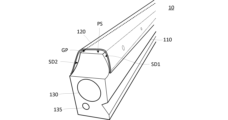
- FIG. 1 is an external view of a press head according to a first embodiment.
- FIG. 2 is an external view of the press head according to the first embodiment.
- FIG. 3 is a side cross-sectional view of the seat portion according to the first embodiment.
- FIG. 4 is a side sectional view showing an overview of heating and pressing electronic components using the press apparatus according to the first embodiment.
- 5(A) to 5(F) are side sectional views schematically showing the shape of the sheet portion when heating and pressurizing the electronic component according to the first embodiment.
- FIG. 6 is a flowchart showing a procedure for processing when applying heat and pressure to the electronic component according to the first embodiment.
- FIG. 1 and 2 are external views of a press head according to a first embodiment.
- FIG. 3 is a side cross-sectional view showing an overview of heating and pressing electronic components using a plurality of press heads according to the first embodiment.
- FIG. 4 is a side sectional view of the seat portion according to the first embodiment.
- 5(A) to 5(F) are side sectional views schematically showing the shape of the sheet portion when heating and pressurizing the electronic component according to the first embodiment.
- FIG. 6 is a flowchart showing a procedure for heating and pressurizing the electronic component according to the first embodiment.
- the press head 10 includes a head body 110 and a seat portion 120.
- the head body 110 also includes a heater portion 130 and a sensor portion 135 inside.
- the press head 10 is heated by the heater portion 130 (heating mechanism).
- the temperature of the heater portion 130 is detected by the sensor portion 135.
- the head main body 110 has a polygonal column shape, for example.
- the head main body 110 includes a press surface PS, a first side surface SD1 connected to the press surface PS, and a second side surface SD2.
- the corners of the part where the press surface PS and the first side surface SD1 are connected, and the part where the press surface PS and the second side surface SD2 are connected (boundary part) are rounded, and the corners of the press surface PS, the first side surface SD1, and the press surface PS are rounded.
- the second side surface SD2 are smoothly connected to each other and have an R-chamfered shape.
- the seat portion 120 is arranged at a position facing the press surface PS of the head main body 110. More specifically, the sheet portion 120 is fixed to the first side surface SD1 and the second side surface SD2 of the head main body 110 with, for example, adhesive tape, and is further fixed so as to face the press surface PS.
- the seat portion 120 is removable.
- the sheet portion 120 is arranged so as to cover the press surface PS along the first side surface SD1 and the second side surface SD2. That is, the sheet portion 120 preferably has a substantially rectangular shape that can cover the press surface PS, and has a shape that corresponds to the size of the press surface PS.
- the seat part 120 is fixed so that a gap GP is provided between the press surface PS and the seat part 120.
- the shape of the gap GP may be any shape that is sufficient to cause the sheet portion 120 to bend when the press head 10 comes into contact with the electronic component during heating and pressurization. The specific configuration will be described later.
- FIG. 3 is a cross-sectional view of the seat portion 120 and the head main body 110. This sectional view is a sectional view taken along a plane perpendicular to the direction in which the head main body 110 extends.
- FIG. 3 schematically represents the structure of the seat portion 120 and the head main body 110.
- the sheet portion 120 includes a release layer 121 and a flexible layer 122.
- the release layer 121 is formed so as to be in contact with the flexible layer 122.
- the seat portion 120 is formed to face the head main body 110 as described above. More specifically, the flexible layer 122 of the sheet portion 120 is formed to face the head main body 110. In other words, the flexible layer 122 is formed to face the press surface PS.
- the release layer 121 is formed so as to be in contact with the flexible layer 122. Note that it is preferable that substantially the entire surface of the sheet portion 120 opposite to the surface facing the head main body 110 is the mold release layer 121 .
- the release layer 121 is made of fluororesin (for example, PTFE). Note that the mold release layer 121 is not limited to PTFE, and may be made of thermoplastic resin or FEP. In other words, any material with low wettability may be used.
- fluororesin for example, PTFE
- FEP thermoplastic resin
- the flexible layer 122 is made of glass fiber, for example.
- the glass fibers may be either glass wool (short fibers) or glass fibers (long fibers). Note that the flexible layer 122 may be formed by knitting glass fibers into a mesh shape.
- the mold release layer 121 and the flexible layer 122 are formed as two separate layers.
- the release layer 121 and the flexible layer 122 may be integrally formed. In other words, substantially the entire surface of the flexible layer 122 may be covered with the release layer 121.
- the press device 1 includes a plurality of press heads 10 (for convenience, they are referred to as a press head 10U1 and a press head 10U2). More specifically, the press surface PS1 of the press head 10U1 and the press surface PS2 of the press head 10U2 in FIG. 4 are arranged at opposing positions.
- the press head 10U1 and the press head 10U2 have the same configuration as the press head 10 described above.
- the electronic component 200 (for example, a solid electrolytic capacitor having a lead frame) is placed between the press surface PS1 and the press surface PS2. In other words, the electronic component 200 is arranged between the seat portion 120A formed in the press head 10U1 and the seat portion 120B formed in the press head 10U2.
- FIGS. 5(A) to 5(F) and FIG. 6 Note that the seat portion 120B of the press head 10U2 is omitted because it moves in substantially the same manner as the press head 10U1.
- Electronic component 200 is, for example, a solid electrolytic capacitor.
- a solid electrolytic capacitor includes a plurality of capacitor elements, and the capacitor elements are joined to a lead frame.
- the plurality of capacitor elements are thicker at a portion that functions as a capacitor than at a region where the lead frame is bonded. Therefore, it has portions with different thicknesses and has an inclination when viewed from the side.
- a bonding material for example, silver paste
- the press head 10U1 is positioned so as to abut against the electronic component 200 (FIG. 6: step S12).
- the sheet portion 120A is not deformed. This is the initial state of the sheet portion 120A.
- press head 10U1 is pressed against electronic component 200.
- the sheet portion 120A begins to deform to conform to the outer shape of the electronic component 200.
- the sheet portion 120A has the flexible layer 122 and is easily deformed because it has the gap GP between the sheet portion 120A and the press surface PS. That is, the flexible layer 122 of the sheet portion 120A serves as a cushioning material, and it is possible to suppress damage to the electronic component 200 caused by the press head 10U1. In other words, the deformation of the flexible layer 122 serves as a cushion, and damage to the electronic component 200 can be suppressed.
- the head main body 110 has an R-chamfered shape. Therefore, damage to the seat portion 120A is suppressed.
- the press head 10U1 is further pressed against the electronic component 200 and heated and pressurized (FIG. 6: Step S13).
- the flexible layer 122 of the sheet portion 120A deforms and follows the external shape of the electronic component 200.
- the shape of the electronic component 200 (laminated body of a plurality of capacitor elements) is exaggerated, and the press head 10U1 and the electronic component 200 are far apart, but in reality, the sheet portion The thickness is close to 120A.
- the electronic component 200 comes into contact with the sheet portion 120A with almost no gap, and the contact area between the sheet portion 120A and the electronic component 200 can be widened. That is, it is possible to suppress the pressure and heating temperature during heating and pressing of the press head 10U1 from concentrating locally (for example, in the case of a solid electrolytic capacitor, at a specific location in the capacitor laminate). Further, pressure and heating temperature are applied evenly to the electronic component 200. Therefore, bonding defects during bonding of the electronic component 200 can be suppressed. For example, a portion where a plurality of capacitor elements are joined to a lead frame is thinner than a portion where capacitor functional parts of a plurality of capacitor elements are stacked. Even with such a configuration, bonding defects can be suppressed.
- the movement of the seat portion 120A when the press head 10U1 is separated from the electronic component 200 after being heated and pressurized will be described.
- the head main body 110 separates from the electronic component 200 first, and the seat portion 120A gradually separates from the end of the electronic component 200.
- the center portion of the seat portion 120A is in contact with the electronic component 200.
- the press head 10U1 is further separated from the electronic component 200 (FIG. 6: Step S14).
- the seat portion 120A gradually separates from the center of the electronic component 200. Specifically, the sheet portion 120A deforms so as to extend in the direction of the electronic component 200, and gradually separates from the outer periphery of the electronic component 200 toward the center.
- the configuration of the present invention and the conventional configuration will be compared.
- electronic components are difficult to peel off from the press head.
- the electronic component is pulled by the press head (upward in FIG. 5(E)). That is, since the electronic component is separated by the press head before the inside of the electronic component is hardened, peeling occurs inside the electronic component.
- the release layer 121 of the sheet portion 120A is in contact with the electronic component 200. Due to the wettability of the release layer 121, the sheet portion 120A is easily peeled off from the electronic component 200. That is, the head main body 110 that is not in direct contact with the electronic component 200 is peeled off first. After that, the seat portion 120A gradually separates from the electronic component 200. Therefore, the sheet portion 120A is separated from the press head 10U1 after the inside of the electronic component 200 is sufficiently hardened. Therefore, peeling inside the electronic component 200 is suppressed.
- the seat portion 120A returns to the initial state shown in FIG. 5(A).
- press head 10 By using the press head 10 (press head 10U1, press head 10U2), the following effects can be obtained.
- the bonding material placed inside the electronic component 200 is melted by the heating temperature of the press head 10.
- This melted bonding material may protrude from the outer surface of the electronic component 200. That is, the melted bonding material adheres to the release layer 121 of the sheet portion 120.
- the bonding material adheres to the press surface, creating unevenness. Therefore, when heating and pressurizing is performed next time, there is a possibility that a bonding failure will occur due to the unevenness.
- the release layer 121 of the sheet portion 120A is provided at a position where it comes into contact with the electronic component 200. That is, even if the bonding material adheres to the release layer 121, it is easy to remove (clean) the bonding material from the release layer 121 of the sheet portion 120A.
- the seat portion 120 has a structure that is removable from the head main body 110.
- the seat portion 120 is worn out by being repeatedly heated and pressurized. However, if the seat portion 120 becomes worn, it can be replaced.
- the electronic component 200 is a solid electrolytic capacitor.
- the press head 10 or the press apparatus 1 of the present invention can be applied when applying a bonding material to a support and fixing a semiconductor element to the bonding material.
- the electronic component 200 is applicable not only to semiconductor devices but also to other electronic components.
- a head body having a press surface; a sheet portion facing the press surface and fixed so as to have a gap with respect to the press surface; Equipped with The sheet portion is a press head including a flexible layer facing the press surface and a release layer formed so as to be in contact with the flexible layer.
- the head main body has a first side surface and a second side surface that are connected to the press surface, The press head according to ⁇ 1>, wherein the seat portion is fixed to the first side surface and the second side surface.
- ⁇ 4> The press head according to any one of ⁇ 1> to ⁇ 3>, wherein the seat portion is removable from the head main body.
- ⁇ 6> The press head according to any one of ⁇ 1> to ⁇ 5>, comprising a heating mechanism inside the head main body.
- ⁇ 7> Equipped with a plurality of press heads according to any one of ⁇ 1> to ⁇ 6>, A press device, wherein the press surfaces of the press heads are arranged at opposing positions.
- a semiconductor manufacturing apparatus comprising the press head according to any one of ⁇ 1> to ⁇ 6> or the press apparatus according to ⁇ 7>.
- An electronic component manufacturing apparatus comprising the press head according to any one of ⁇ 1> to ⁇ 6> or the press apparatus according to ⁇ 7>.
Landscapes
- Engineering & Computer Science (AREA)
- Manufacturing & Machinery (AREA)
- Microelectronics & Electronic Packaging (AREA)
- Wire Bonding (AREA)
Priority Applications (2)
| Application Number | Priority Date | Filing Date | Title |
|---|---|---|---|
| CN202380062426.7A CN119768904A (zh) | 2022-09-20 | 2023-09-06 | 压制头、压制装置、半导体制造装置以及电子部件制造装置 |
| JP2024548186A JP7816546B2 (ja) | 2022-09-20 | 2023-09-06 | プレスヘッド、プレス装置、半導体製造装置、および電子部品製造装置 |
Applications Claiming Priority (2)
| Application Number | Priority Date | Filing Date | Title |
|---|---|---|---|
| JP2022-148963 | 2022-09-20 | ||
| JP2022148963 | 2022-09-20 |
Publications (1)
| Publication Number | Publication Date |
|---|---|
| WO2024062921A1 true WO2024062921A1 (ja) | 2024-03-28 |
Family
ID=90454235
Family Applications (1)
| Application Number | Title | Priority Date | Filing Date |
|---|---|---|---|
| PCT/JP2023/032475 Ceased WO2024062921A1 (ja) | 2022-09-20 | 2023-09-06 | プレスヘッド、プレス装置、半導体製造装置、および電子部品製造装置 |
Country Status (3)
| Country | Link |
|---|---|
| JP (1) | JP7816546B2 (https=) |
| CN (1) | CN119768904A (https=) |
| WO (1) | WO2024062921A1 (https=) |
Citations (3)
| Publication number | Priority date | Publication date | Assignee | Title |
|---|---|---|---|---|
| JP2004335627A (ja) * | 2003-05-06 | 2004-11-25 | Nippon Tungsten Co Ltd | 加熱圧着用ツール及びその製造方法 |
| JP2010016070A (ja) * | 2008-07-02 | 2010-01-21 | Nec Engineering Ltd | 半導体チップの実装装置 |
| JP2017120835A (ja) * | 2015-12-28 | 2017-07-06 | 富士通株式会社 | 半導体実装装置、半導体実装装置のヘッド及び積層チップの製造方法 |
-
2023
- 2023-09-06 WO PCT/JP2023/032475 patent/WO2024062921A1/ja not_active Ceased
- 2023-09-06 JP JP2024548186A patent/JP7816546B2/ja active Active
- 2023-09-06 CN CN202380062426.7A patent/CN119768904A/zh active Pending
Patent Citations (3)
| Publication number | Priority date | Publication date | Assignee | Title |
|---|---|---|---|---|
| JP2004335627A (ja) * | 2003-05-06 | 2004-11-25 | Nippon Tungsten Co Ltd | 加熱圧着用ツール及びその製造方法 |
| JP2010016070A (ja) * | 2008-07-02 | 2010-01-21 | Nec Engineering Ltd | 半導体チップの実装装置 |
| JP2017120835A (ja) * | 2015-12-28 | 2017-07-06 | 富士通株式会社 | 半導体実装装置、半導体実装装置のヘッド及び積層チップの製造方法 |
Also Published As
| Publication number | Publication date |
|---|---|
| CN119768904A (zh) | 2025-04-04 |
| JPWO2024062921A1 (https=) | 2024-03-28 |
| JP7816546B2 (ja) | 2026-02-18 |
Similar Documents
| Publication | Publication Date | Title |
|---|---|---|
| JP2008012918A (ja) | 積層装置およびそれを用いた積層方法 | |
| JP2011108929A (ja) | 回路基板および回路基板の製造方法 | |
| KR101827869B1 (ko) | 박리 접합 동시 수행 장치 및 방법 | |
| JP7816546B2 (ja) | プレスヘッド、プレス装置、半導体製造装置、および電子部品製造装置 | |
| WO2018122683A1 (en) | Method for manufacturing sheet laminate, mold for molding sheet laminate, and sheet laminate | |
| KR100474646B1 (ko) | 적층체의 제조 방법과 적층체 가압 장치 | |
| JP4201882B2 (ja) | 積層板の製造方法 | |
| JP4175192B2 (ja) | 多層基板の製造方法 | |
| JP3876802B2 (ja) | プレス工法 | |
| JP4548210B2 (ja) | 多層回路基板の製造方法 | |
| JP7686179B1 (ja) | 半導体モジュールの製造方法及び電子装置の製造方法 | |
| JP4114787B2 (ja) | 真空積層装置及び積層方法 | |
| JP4311120B2 (ja) | 多層基板の製造方法及び熱プレス機 | |
| WO2008069018A1 (ja) | 凹凸パターン形成方法 | |
| JP5310652B2 (ja) | 複合基板の製造方法 | |
| CN111742623A (zh) | 带金属片配线基板以及带金属片配线基板的制造方法 | |
| KR102252762B1 (ko) | Fpcb 제조용 핫프레스의 압착헤드 | |
| CN103037638B (zh) | 带有芯片窗口的待压合多层板的压合方法 | |
| JP2003236700A (ja) | 積層プレスのためのプレスラム | |
| JP2001189553A (ja) | 基板の接合装置及びその装置を用いた基板の接合方法 | |
| TW529316B (en) | Method for making composite plate | |
| JP3243608B2 (ja) | 真空積層装置および真空積層方法 | |
| JP2025085166A (ja) | ガラス積層体の製造方法及びガラス積層体 | |
| JP3985304B2 (ja) | プリント配線板の製造方法 | |
| JP2000141389A (ja) | 真空積層装置および真空積層方法 |
Legal Events
| Date | Code | Title | Description |
|---|---|---|---|
| 121 | Ep: the epo has been informed by wipo that ep was designated in this application |
Ref document number: 23868044 Country of ref document: EP Kind code of ref document: A1 |
|
| WWE | Wipo information: entry into national phase |
Ref document number: 2024548186 Country of ref document: JP |
|
| WWE | Wipo information: entry into national phase |
Ref document number: 202380062426.7 Country of ref document: CN |
|
| WWP | Wipo information: published in national office |
Ref document number: 202380062426.7 Country of ref document: CN |
|
| NENP | Non-entry into the national phase |
Ref country code: DE |
|
| 122 | Ep: pct application non-entry in european phase |
Ref document number: 23868044 Country of ref document: EP Kind code of ref document: A1 |