WO2024053679A1 - セラミック構造体 - Google Patents
セラミック構造体 Download PDFInfo
- Publication number
- WO2024053679A1 WO2024053679A1 PCT/JP2023/032556 JP2023032556W WO2024053679A1 WO 2024053679 A1 WO2024053679 A1 WO 2024053679A1 JP 2023032556 W JP2023032556 W JP 2023032556W WO 2024053679 A1 WO2024053679 A1 WO 2024053679A1
- Authority
- WO
- WIPO (PCT)
- Prior art keywords
- layer
- void
- ceramic structure
- structure according
- crystal grain
- Prior art date
- Legal status (The legal status is an assumption and is not a legal conclusion. Google has not performed a legal analysis and makes no representation as to the accuracy of the status listed.)
- Ceased
Links
Images


Classifications
-
- C—CHEMISTRY; METALLURGY
- C04—CEMENTS; CONCRETE; ARTIFICIAL STONE; CERAMICS; REFRACTORIES
- C04B—LIME, MAGNESIA; SLAG; CEMENTS; COMPOSITIONS THEREOF, e.g. MORTARS, CONCRETE OR LIKE BUILDING MATERIALS; ARTIFICIAL STONE; CERAMICS; REFRACTORIES; TREATMENT OF NATURAL STONE
- C04B35/00—Shaped ceramic products characterised by their composition; Ceramics compositions; Processing powders of inorganic compounds preparatory to the manufacturing of ceramic products
- C04B35/515—Shaped ceramic products characterised by their composition; Ceramics compositions; Processing powders of inorganic compounds preparatory to the manufacturing of ceramic products based on non-oxide ceramics
- C04B35/58—Shaped ceramic products characterised by their composition; Ceramics compositions; Processing powders of inorganic compounds preparatory to the manufacturing of ceramic products based on non-oxide ceramics based on borides, nitrides, i.e. nitrides, oxynitrides, carbonitrides or oxycarbonitrides or silicides
- C04B35/581—Shaped ceramic products characterised by their composition; Ceramics compositions; Processing powders of inorganic compounds preparatory to the manufacturing of ceramic products based on non-oxide ceramics based on borides, nitrides, i.e. nitrides, oxynitrides, carbonitrides or oxycarbonitrides or silicides based on aluminium nitride
-
- C—CHEMISTRY; METALLURGY
- C23—COATING METALLIC MATERIAL; COATING MATERIAL WITH METALLIC MATERIAL; CHEMICAL SURFACE TREATMENT; DIFFUSION TREATMENT OF METALLIC MATERIAL; COATING BY VACUUM EVAPORATION, BY SPUTTERING, BY ION IMPLANTATION OR BY CHEMICAL VAPOUR DEPOSITION, IN GENERAL; INHIBITING CORROSION OF METALLIC MATERIAL OR INCRUSTATION IN GENERAL
- C23C—COATING METALLIC MATERIAL; COATING MATERIAL WITH METALLIC MATERIAL; SURFACE TREATMENT OF METALLIC MATERIAL BY DIFFUSION INTO THE SURFACE, BY CHEMICAL CONVERSION OR SUBSTITUTION; COATING BY VACUUM EVAPORATION, BY SPUTTERING, BY ION IMPLANTATION OR BY CHEMICAL VAPOUR DEPOSITION, IN GENERAL
- C23C16/00—Chemical coating by decomposition of gaseous compounds, without leaving reaction products of surface material in the coating, i.e. chemical vapour deposition [CVD] processes
- C23C16/22—Chemical coating by decomposition of gaseous compounds, without leaving reaction products of surface material in the coating, i.e. chemical vapour deposition [CVD] processes characterised by the deposition of inorganic material, other than metallic material
- C23C16/30—Deposition of compounds, mixtures or solid solutions, e.g. borides, carbides, nitrides
- C23C16/34—Nitrides
-
- C—CHEMISTRY; METALLURGY
- C04—CEMENTS; CONCRETE; ARTIFICIAL STONE; CERAMICS; REFRACTORIES
- C04B—LIME, MAGNESIA; SLAG; CEMENTS; COMPOSITIONS THEREOF, e.g. MORTARS, CONCRETE OR LIKE BUILDING MATERIALS; ARTIFICIAL STONE; CERAMICS; REFRACTORIES; TREATMENT OF NATURAL STONE
- C04B41/00—After-treatment of mortars, concrete, artificial stone or ceramics; Treatment of natural stone
- C04B41/009—After-treatment of mortars, concrete, artificial stone or ceramics; Treatment of natural stone characterised by the material treated
-
- C—CHEMISTRY; METALLURGY
- C04—CEMENTS; CONCRETE; ARTIFICIAL STONE; CERAMICS; REFRACTORIES
- C04B—LIME, MAGNESIA; SLAG; CEMENTS; COMPOSITIONS THEREOF, e.g. MORTARS, CONCRETE OR LIKE BUILDING MATERIALS; ARTIFICIAL STONE; CERAMICS; REFRACTORIES; TREATMENT OF NATURAL STONE
- C04B41/00—After-treatment of mortars, concrete, artificial stone or ceramics; Treatment of natural stone
- C04B41/45—Coating or impregnating, e.g. injection in masonry, partial coating of green or fired ceramics, organic coating compositions for adhering together two concrete elements
- C04B41/4505—Coating or impregnating, e.g. injection in masonry, partial coating of green or fired ceramics, organic coating compositions for adhering together two concrete elements characterised by the method of application
- C04B41/4529—Coating or impregnating, e.g. injection in masonry, partial coating of green or fired ceramics, organic coating compositions for adhering together two concrete elements characterised by the method of application applied from the gas phase
-
- C—CHEMISTRY; METALLURGY
- C04—CEMENTS; CONCRETE; ARTIFICIAL STONE; CERAMICS; REFRACTORIES
- C04B—LIME, MAGNESIA; SLAG; CEMENTS; COMPOSITIONS THEREOF, e.g. MORTARS, CONCRETE OR LIKE BUILDING MATERIALS; ARTIFICIAL STONE; CERAMICS; REFRACTORIES; TREATMENT OF NATURAL STONE
- C04B41/00—After-treatment of mortars, concrete, artificial stone or ceramics; Treatment of natural stone
- C04B41/45—Coating or impregnating, e.g. injection in masonry, partial coating of green or fired ceramics, organic coating compositions for adhering together two concrete elements
- C04B41/50—Coating or impregnating, e.g. injection in masonry, partial coating of green or fired ceramics, organic coating compositions for adhering together two concrete elements with inorganic materials
- C04B41/5053—Coating or impregnating, e.g. injection in masonry, partial coating of green or fired ceramics, organic coating compositions for adhering together two concrete elements with inorganic materials non-oxide ceramics
- C04B41/5062—Borides, Nitrides or Silicides
- C04B41/5063—Aluminium nitride
-
- C—CHEMISTRY; METALLURGY
- C04—CEMENTS; CONCRETE; ARTIFICIAL STONE; CERAMICS; REFRACTORIES
- C04B—LIME, MAGNESIA; SLAG; CEMENTS; COMPOSITIONS THEREOF, e.g. MORTARS, CONCRETE OR LIKE BUILDING MATERIALS; ARTIFICIAL STONE; CERAMICS; REFRACTORIES; TREATMENT OF NATURAL STONE
- C04B41/00—After-treatment of mortars, concrete, artificial stone or ceramics; Treatment of natural stone
- C04B41/80—After-treatment of mortars, concrete, artificial stone or ceramics; Treatment of natural stone of only ceramics
- C04B41/81—Coating or impregnation
- C04B41/85—Coating or impregnation with inorganic materials
- C04B41/87—Ceramics
-
- C—CHEMISTRY; METALLURGY
- C04—CEMENTS; CONCRETE; ARTIFICIAL STONE; CERAMICS; REFRACTORIES
- C04B—LIME, MAGNESIA; SLAG; CEMENTS; COMPOSITIONS THEREOF, e.g. MORTARS, CONCRETE OR LIKE BUILDING MATERIALS; ARTIFICIAL STONE; CERAMICS; REFRACTORIES; TREATMENT OF NATURAL STONE
- C04B2111/00—Mortars, concrete or artificial stone or mixtures to prepare them, characterised by specific function, property or use
- C04B2111/00241—Physical properties of the materials not provided for elsewhere in C04B2111/00
- C04B2111/00405—Materials with a gradually increasing or decreasing concentration of ingredients or property from one layer to another
-
- C—CHEMISTRY; METALLURGY
- C04—CEMENTS; CONCRETE; ARTIFICIAL STONE; CERAMICS; REFRACTORIES
- C04B—LIME, MAGNESIA; SLAG; CEMENTS; COMPOSITIONS THEREOF, e.g. MORTARS, CONCRETE OR LIKE BUILDING MATERIALS; ARTIFICIAL STONE; CERAMICS; REFRACTORIES; TREATMENT OF NATURAL STONE
- C04B2235/00—Aspects relating to ceramic starting mixtures or sintered ceramic products
- C04B2235/02—Composition of constituents of the starting material or of secondary phases of the final product
- C04B2235/30—Constituents and secondary phases not being of a fibrous nature
- C04B2235/38—Non-oxide ceramic constituents or additives
- C04B2235/3852—Nitrides, e.g. oxynitrides, carbonitrides, oxycarbonitrides, lithium nitride, magnesium nitride
- C04B2235/3865—Aluminium nitrides
-
- C—CHEMISTRY; METALLURGY
- C04—CEMENTS; CONCRETE; ARTIFICIAL STONE; CERAMICS; REFRACTORIES
- C04B—LIME, MAGNESIA; SLAG; CEMENTS; COMPOSITIONS THEREOF, e.g. MORTARS, CONCRETE OR LIKE BUILDING MATERIALS; ARTIFICIAL STONE; CERAMICS; REFRACTORIES; TREATMENT OF NATURAL STONE
- C04B2235/00—Aspects relating to ceramic starting mixtures or sintered ceramic products
- C04B2235/70—Aspects relating to sintered or melt-casted ceramic products
- C04B2235/74—Physical characteristics
- C04B2235/76—Crystal structural characteristics, e.g. symmetry
- C04B2235/767—Hexagonal symmetry, e.g. beta-Si3N4, beta-Sialon, alpha-SiC or hexa-ferrites
-
- C—CHEMISTRY; METALLURGY
- C04—CEMENTS; CONCRETE; ARTIFICIAL STONE; CERAMICS; REFRACTORIES
- C04B—LIME, MAGNESIA; SLAG; CEMENTS; COMPOSITIONS THEREOF, e.g. MORTARS, CONCRETE OR LIKE BUILDING MATERIALS; ARTIFICIAL STONE; CERAMICS; REFRACTORIES; TREATMENT OF NATURAL STONE
- C04B2235/00—Aspects relating to ceramic starting mixtures or sintered ceramic products
- C04B2235/70—Aspects relating to sintered or melt-casted ceramic products
- C04B2235/94—Products characterised by their shape
- C04B2235/945—Products containing grooves, cuts, recesses or protusions
-
- C—CHEMISTRY; METALLURGY
- C04—CEMENTS; CONCRETE; ARTIFICIAL STONE; CERAMICS; REFRACTORIES
- C04B—LIME, MAGNESIA; SLAG; CEMENTS; COMPOSITIONS THEREOF, e.g. MORTARS, CONCRETE OR LIKE BUILDING MATERIALS; ARTIFICIAL STONE; CERAMICS; REFRACTORIES; TREATMENT OF NATURAL STONE
- C04B2235/00—Aspects relating to ceramic starting mixtures or sintered ceramic products
- C04B2235/70—Aspects relating to sintered or melt-casted ceramic products
- C04B2235/96—Properties of ceramic products, e.g. mechanical properties such as strength, toughness, wear resistance
Definitions
- the disclosed embodiments relate to ceramic structures.
- Patent Document 1 a ceramic structure having a thin film formed by chemical vapor deposition (CVD) is known.
- Patent Document 2 describes that a film formed by chemical vapor deposition is dense, has no voids, and has high smoothness.
- Patent Document 3 describes that the content of pores is less than 3% by area.
- a ceramic structure includes a first layer having first crystal grains, and a second layer located on the first layer and having second crystal grains.
- the first crystal particles and the second crystal particles each contain one or more metal elements selected from Al, Si, Ti, Cr, Zr, and Y, and one or more nonmetals selected from N, C, and B. Contains the elements.
- the first crystal particles and the second crystal particles are the same compound.
- the half width of the peak of the Miller index of the maximum intensity of the first crystal grain in the X-ray diffraction of the first layer is W1, which is the same as the Miller index of the second crystal grain in the X-ray diffraction of the second layer. When the half width of the peak is W2, 9 ⁇ W1>W2>W1.
- FIG. 1 is a sectional view showing an example of a ceramic structure according to an embodiment.
- FIG. 2 is an enlarged view of area A shown in FIG.
- FIG. 3 is a sectional view showing another example of the ceramic structure according to the embodiment.
- FIG. 4 is a sectional view showing another example of the ceramic structure according to the embodiment.
- FIG. 5 is a sectional view showing another example of the ceramic structure according to the embodiment.
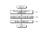
- FIG. 6 is a flowchart illustrating an example of a method for manufacturing a ceramic structure according to an embodiment.
- FIG. 1 is a sectional view showing an example of a ceramic structure according to an embodiment.
- the ceramic structure 1 has a first layer 10 and a second layer 20.
- the first layer 10 has first crystal grains 11 .
- the second layer 20 has second crystal grains 21 .
- the first crystal grains 11 and the second crystal grains 21 each contain one or more metal elements selected from Al, Si, Ti, Cr, Zr, and Y, and one or more non-metal elements selected from N, C, and B. Contains a metal element.
- the first layer 10 may contain the first crystal grains 11 in an area of 50% or more.
- the first layer 10 may contain 80 area % or more of the first crystal grains 11.
- the first layer 10 may contain 90 area % or more of the first crystal grains 11.
- the second layer 20 may contain the second crystal grains 21 in an area of 50% or more.
- the second layer 20 may contain the second crystal particles 21 in an area of 80% or more.
- the second layer 20 may contain 90 area % or more of the second crystal particles 21.
- the amount of second crystal particles 21 included in the second layer 20 may be greater than the amount of first crystal particles 11 included in the first layer 10.
- the first crystal particles 11 and the second crystal particles 21 are the same compound.
- the first crystal particles 11 and the second crystal particles 21 may be made of AlN, Si 3 N 4 , SiC, TiN, TiC, ZrN, ZrB, or YN.
- the first crystal particles 11 may be AlN.
- AlN it is sufficient that the two compounds have Al and N as main components and can be identified as AlN by XRD.
- the content of Al may be different between the first crystal grains 11 and the second crystal grains 21.
- the half width of the peak of the Miller index of the maximum intensity of the first crystal grains 11 in the X-ray diffraction of the first layer 10 is W1
- the half width of the same peak as the Miller index of the second crystal grains 21 in the X-ray diffraction of the second layer 20 is W1.
- W2>W1 means that the degree of crystallinity of the second crystal grains 21 is lower than the degree of crystallinity of the first crystal grains 11.
- 9 ⁇ W1>W2 means that the half-width of W2 is smaller than nine times the half-width of W1.
- the relationship between W1 and W2 may be 8.5 ⁇ W1>W2.
- the relationship between W1 and W2 may be 8.0 ⁇ W1>W2.
- the relationship between W1 and W2 may be 6.9 ⁇ W1>W2.
- W1, W2, and W3, which will be described later, can be measured by the following method.
- Low-angle incidence measurements are performed using a thin film X-ray diffractometer, X'Pert PRO-MRD (DY1878) manufactured by PANalytical.
- the optical system includes an X-ray mirror (automatic insertion attenuation plate, mask 5, solar slit 0.02 rad, slit 1/8), flat plate collimator, tube: CuK ⁇ , X-ray: 45 kV, 40 mA, 2 ⁇ scan: 10° to 100 angle of incidence: 0.1°, step: 0.02°, time: 4.0 seconds/step.
- X-ray mirror automated insertion attenuation plate, mask 5, solar slit 0.02 rad, slit 1/8
- flat plate collimator tube: CuK ⁇
- X-ray 45 kV
- 2 ⁇ scan 10° to 100 angle of incidence: 0.1°
- time 4.0 seconds/step.
- the first layer 10 is a base, and may have a substantially disk shape, for example.
- the second layer 20 is located on the base (first layer 10), and the second layer 20 may be in contact with the base (first layer 10).
- the base contains ceramic such as aluminum nitride (AlN) as a main component, for example.
- the first layer 10 may contain, for example, aluminum oxide (Al 2 O 3 ), yttria (Y 2 O 3 ), or the like as a main component.
- the first layer 10 may be a sintered body obtained by firing raw material powder. When the first layer 10 is a sintered body, the first crystal grains 11 have a high degree of crystallinity. With such a configuration, a ceramic structure with excellent durability can be provided.
- first crystal grains 11 and the second crystal grains 21 may be hexagonal.
- the crystal has anisotropy, and by utilizing this anisotropy, a ceramic structure with excellent durability can be provided.
- first crystal grain 11 and the second crystal grain 21 may be AlN, and the difference between W1 and W2 (W2-W1) described above may be 0.1° or more and 0.6° or less.
- W1 and W2 W2-W1
- the difference in physical properties between the first layer 10 and the second layer 20 can be reduced while providing the second layer 20 that is different from the first layer 10, resulting in a highly durable ceramic structure. You can donate your body.
- the second layer 20 may have voids 22 located inside the second layer 20.
- the void 22 may be long in the thickness direction of the second layer 20 and may be closed at both ends in the thickness direction.
- the void 22 may have at least one of a first void 22a whose one end in the thickness direction is in contact with the first layer 10 and a second void 22b whose one end is separated from the first layer 10.
- the void 22 may have an elongated shape that is longer in the thickness direction of the second layer 20 than in the width direction.
- the void 22 may be closed at both ends in the thickness direction of the second layer 20. That is, the void 22 is located between the first surface 201 of the second layer 20 facing the first layer 10 and the second surface 202 opposite to the first surface 201, and is located at the interface with the outside. A certain second surface 202 is not exposed. Therefore, the second layer 20 has desired durability even if it has voids 22 inside.
- the voids 22 are not lattice defects or so-called nanovoids that may exist in the second crystal grains 21.
- the width of the void 22 may be, for example, 0.01 ⁇ m or more.
- the width of the void 22 may be, for example, 0.05 ⁇ m or more.
- the width of the void 22 may be, for example, 1 ⁇ m or less.
- the width of the void 22 may be, for example, 0.5 ⁇ m or less.
- the length of the void 22 may be, for example, 0.2 ⁇ m or more.
- the length of the void 22 may be, for example, 0.5 ⁇ m or more.
- the length of the void 22 may be, for example, 5 ⁇ m or less.
- the length of the void 22 may be, for example, 1 ⁇ m or less.
- the presence or absence of the voids 22 can be confirmed, for example, by observation using an electron microscope.
- the area ratio of the voids 22 in the second layer 20 may be, for example, 0.2 area % or more.
- the area ratio of the voids 22 may be, for example, 1 area % or more.
- the area ratio of the voids 22 may be, for example, 5 area % or less.
- the area ratio of the voids 22 may be, for example, 3 area % or less.
- the area ratio of the voids 22 in the second layer 20 may be measured, for example, at the center of the cross section of the second layer 20 after mirror-finishing the cross section. Observation with an electron microscope may be performed at a magnification of 1,000 times to 50,000 times.
- the electron microscope may be, for example, JSM7900F manufactured by JEOL Ltd., with an accelerating voltage of 5.0 KV.
- the area ratio of the voids 22 may be calculated using image analysis software IMAGE Pro10 manufactured by MEDIA CYBERNETICS based on the SEM photograph.
- the SEM photograph may be binarized using the Ward method and the binarized image may be used for calculation.
- the void 22 may have a first void 22a and a second void 22b.
- the first void 22a is a void 22 whose lower end, which is one end in the thickness direction of the second layer 20, is in contact with the surface 101 of the first layer 10.
- the second void 22b is a void 22 with one end separated from the surface 101 of the first layer 10.
- the second layer 20 may have both the first void 22a and the second void 22b inside, or may have only one of them.
- FIG. 2 is an enlarged view of area A shown in FIG.
- the second crystal particles 21 included in the second layer 20 may include columnar crystals 21a.
- the columnar crystals 21a extend, for example, in a direction intersecting the surface 101 of the first layer 10. That is, the columnar crystals 21a extend in the thickness direction of the second layer 20.
- the second layer 20 may include a plurality of columnar crystals 21a arranged along the surface 101 of the first layer 10. Since the second crystal grains 21 have columnar crystals 21a, the second layer 20 has improved thermal conductivity in the thickness direction. Therefore, the temperature variation in the thickness direction of the second layer 20 is reduced, and the durability is improved.
- the width of the void 22, that is, the length of the void 22 in the direction along the surface 101 of the first layer 10, is set to be farther away from the first layer 10 than the first end 221 in the thickness direction located on the first layer 10 side.
- the second end portion 222 may be smaller. This makes it difficult for the void 22 to become a crack and spread from the second end 222 toward the second surface 202 . Therefore, the durability of the ceramic structure 1 including the second layer 20 is improved.
- the void 22 may be located between adjacent columnar crystals 21a.
- the voids 22 may be larger or smaller than the columnar crystals 21a.
- a space 40 may be provided between the first layer 10 and the second layer 20.
- the space 40 refers to a space extending along the surface 101 of the first layer 10. More specifically, in cross-sectional view, the length of the space 40 in the direction along the surface 101 connecting both ends with an imaginary line segment is longer than the maximum height of the space 40 in the direction intersecting the surface 101. . More specifically, the length connecting both ends of the space 40 in the direction along the surface 101 with an imaginary line segment is 5 times or more the height of the space 40 in the direction intersecting the surface 101, and preferably 10 times or more. That's more than double that.
- the porosity of the second layer 20 may be greater in the first portion, which is a portion closer to the first layer 10, than in the second portion, which is a portion farther from the first layer 10 than the first portion.
- the thermal conductivity of the first portion can be made smaller than the thermal conductivity of the second portion. Therefore, when a thermal shock is applied to the ceramic structure 1 from the second layer 20 side, a sudden change in the temperature difference that occurs between the first layer 10 and the second layer 20 is suppressed. As a result, the durability of the ceramic structure 1 against thermal shock is improved.
- first portion may be, for example, a region including the first surface 201 in the above-described SEM image
- second portion may be, for example, a region including the second surface 202 in the above-described SEM image. It's okay. Further, the first portion and the second portion may partially overlap.
- the second layer 20 may have a plurality of columnar crystals 21a inclined with respect to the surface 101 of the first layer 10. Further, the void 22 may be located between a plurality of adjacent columnar crystals 21a. As a result, when the tips of the columnar crystals 21a come into contact with the voids 22, the residual stress of the columnar crystals 21a is reduced, so that the durability of the second layer 20 is improved.
- FIG. 3 shows the first gap 22a as an example of the gap 22, it may be the second gap 22b.
- the first layer 10 may have irregularities on the surface 101 facing the second layer 20.
- the first end 221 of the void 22, which is one end in the thickness direction, may be located within the recess 101b of the first layer 10. This prevents the gap 22 from expanding in the direction along the surface 101 of the first layer 10 at the first end 221 .
- the generation of cracks in the columnar crystal 21a adjacent to the first end 221 is suppressed, and the durability of the ceramic structure 1 is improved.
- the void 22 is located above the convex portion 101a of the first layer 10.
- FIG. 4 shows the first gap 22a as an example of the gap 22, it may be the second gap 22b.
- the void 22 may be located above the convex portion 101a of the first layer 10. Further, in FIG. 4, an example in which the plurality of columnar crystals 21a extend along the thickness direction of the second layer 20 has been described. It may extend obliquely from the thickness direction.
- the volume resistivity of the second layer 20 at 25°C may be larger than the volume resistivity of the first layer 10 at 25°C.
- the volume resistivity of the second layer 20 at 500°C may be larger than the volume resistivity of the first layer 10 at 500°C.
- the volume resistivity of the second layer 20 at 25° C. may be 1 ⁇ 10 12 ⁇ m or more.
- the volume resistivity of the second layer 20 at 500° C. may be 1 ⁇ 10 5 ⁇ m or more.
- the volume resistivity of the second layer 20 and the first layer 10 may be measured by a three-terminal method based on JIS C 2141:1992.
- the ceramic structure 1 may have a conductive layer inside.
- the conductive layer may have a heater function. Further, the conductive layer may have an adsorption function.
- the conductive layer may include, for example, W, Mo, Ni, Pt, etc. as a metal.
- the ceramic structure 1 may further include a third layer 30 located between the first layer 10 and the second layer 20.
- the third layer 30 contains third crystal particles 31 that are the same compound as the second layer 20.
- the third layer 30 may have the third crystal grains 31 as a main component.
- the third layer 30 may contain 50 area % or more of the third crystal grains 31.
- the third layer 30 may contain 80 area % or more of the third crystal grains 31.
- the third layer 30 may contain 90 area % or more of the third crystal grains 31.
- W3 is the half-width of the same peak as the Miller index of the second crystal grains 21 in the X-ray diffraction of the third layer 30 of the third crystal grains 31, W2>W3 may be satisfied. Further, 9 ⁇ W3>W2 may be satisfied.
- the relationship between W3 and W2 may be 8.5 ⁇ W3>W2.
- the relationship between W3 and W2 may be 8.0 ⁇ W3>W2.
- the relationship between W3 and W2 may be 6.9 ⁇ W3>W2.
- FIG. 6 is a flowchart illustrating an example of a method for manufacturing a ceramic structure according to an embodiment.
- a sintered body containing 90% by mass to 99.9% by mass of disc-shaped AlN is prepared as a base (first layer 10). Then, a second layer containing AlN as a main component is formed on the surface of this substrate by the following procedure.
- a catalyst is made to act on the first gas (step S11).
- the first gas it is preferable to use one containing nitrogen, and for example, ammonia can be used.
- ammonia can be used.
- tungsten can be used as the catalyst.
- the first gas is decomposed by the catalytic action and a plurality of active species are generated.
- step S11 the active species generated in step S11 and the second gas are supplied to the first layer 10 (step S12).
- the active species generated in step S11 and the second gas are supplied to the first layer 10 (step S12).
- trimethylaluminum can be used as the second gas.
- the second layer 20 is generated on the first layer 10 (step S13).
- the first layer 10 may be heated if necessary.
- the temperature of the first layer 10 can be set, for example, to about 420°C to 1000°C, particularly about 600°C to 700°C.
- the film forming time may be, for example, 0.5 hours to 20 hours depending on the desired thickness.
- a ceramic structure 1 can be obtained which has a second layer 20 having a different crystal structure on the first layer 10 depending on the temperature set during film formation and the like.
- AlN sintered body containing 98% by mass of AlN crystals as the main phase was prepared.
- This AlN sintered body was processed into a first layer having a size of 100 mm square.
- a conductive layer containing W as a metal is disposed inside this AlN sintered body.
- This conductive layer is formed into a heater pattern.
- a second layer was formed on one surface of the first layer using ammonia as the first gas, trimethylaluminum as the second gas, and tungsten as the catalyst.
- the film forming temperature is shown in Table 1.
- W1 and W2 of the obtained ceramic structure were measured.
- W1 and W2 are shown in Table 1.
- the above-mentioned AlN sintered body without the second layer was used. In the case of this sample, the half width of the portion corresponding to the first layer and the portion corresponding to the second layer are the same.
- Table 1 shows the film forming temperature and the above measured values.
- blank columns indicate unmeasured or uncalculated values.
- each of the obtained samples was subjected to mirror polishing, and then a plasma etching resistance test using CF 4 gas was conducted to evaluate the etching rate.
- a high etching rate means poor plasma etching resistance.
- Sample No. 1 is a comparative example in which the parts corresponding to the first layer and the second layer are made of a sintered body.
- sample No. Sample No. 1 is sample No. 1 whose surface roughness after the etching test is an example. It was bigger than 4.
- sample No. Sample No. 1 shows no change in surface roughness before and after the etching test. It was bigger than 4. This is considered to be because the crystals present on the surface of the sintered body were shed during the etching test. Such shedding can become a problem when using a ceramic structure as a member for semiconductor manufacturing equipment.
- sample No. which is an example. No. 4 had excellent surface quality due to mirror polishing.
- sample No. No. 4 had excellent durability in the etching test.
- sample No. In No. 4 the surface roughness after etching was also very good, and it seems that grain shedding was suppressed.
- the ceramic structure includes a first layer having first crystal grains; a second layer located on the first layer and having second crystal particles;
- the first crystal grain and the second crystal grain each have one or more metal elements selected from Al, Si, Ti, Cr, Zr and Y; Contains one or more nonmetallic elements selected from N, C and B,
- the first crystal particles and the second crystal particles are the same compound,
- the half width of the peak of the Miller index of the maximum intensity of the first crystal grain in the X-ray diffraction of the first layer is W1, which is the same as the Miller index of the second crystal grain in the X-ray diffraction of the second layer.
- W1 the half width of the peak
- W2 9 ⁇ W1>W2>W1.
- the first crystal grains and the second crystal grains may be hexagonal crystals.
- the first crystal grains and the second crystal grains are AlN,
- the difference (W2-W1) between the W1 and the W2 may be 0.1° or more and 0.6° or less.
- the second layer has a void located inside the second layer, and the void is located inside the second layer. It is long in the thickness direction, and both ends in the thickness direction are closed,
- the void may have at least one of a first void whose one end in the thickness direction is in contact with the first layer, and a second void whose one end is separated from the first layer.
- the void may include the first void.
- the second layer may have a porosity of 0.1 area % or more and 2 area % or less in a cross section parallel to the thickness direction.
- the second layer has a plurality of columnar crystals tilted with respect to the surface of the first layer,
- the void may be located between the plurality of adjacent columnar crystals.
- the first layer has unevenness on the surface facing the second layer, One end of the void in the thickness direction may be located within the recess of the first layer.
- the length of the void in the direction along the surface of the first layer is the length of the void in the thickness direction located on the first layer side.
- the second end portion remote from the first layer may be smaller than the first end portion.
- the second layer has a first portion closer to the first layer than the first portion.
- the porosity may be greater than that of the second portion that is further away from the second portion.
- the ceramic structure according to any one of (1) to (10) above may have a conductive layer inside.
- the ceramic structure according to any one of (1) to (11) above may further include a third layer located between the first layer and the second layer.
- the third layer contains third crystal particles that are the same compound as the second layer, When W3 is the half-value width of the same peak as the Miller index of the second crystal grain in the X-ray diffraction of the third layer of the third crystal grain, W2>W3 may be satisfied.
Landscapes
- Chemical & Material Sciences (AREA)
- Engineering & Computer Science (AREA)
- Ceramic Engineering (AREA)
- Organic Chemistry (AREA)
- Materials Engineering (AREA)
- Structural Engineering (AREA)
- Inorganic Chemistry (AREA)
- Manufacturing & Machinery (AREA)
- General Chemical & Material Sciences (AREA)
- Chemical Kinetics & Catalysis (AREA)
- Mechanical Engineering (AREA)
- Metallurgy (AREA)
- Ceramic Products (AREA)
- Laminated Bodies (AREA)
Priority Applications (4)
| Application Number | Priority Date | Filing Date | Title |
|---|---|---|---|
| JP2024545692A JPWO2024053679A1 (https=) | 2022-09-09 | 2023-09-06 | |
| EP23863217.8A EP4585580A1 (en) | 2022-09-09 | 2023-09-06 | Ceramic structure |
| CN202380063674.3A CN119731136A (zh) | 2022-09-09 | 2023-09-06 | 陶瓷构造体 |
| US19/109,373 US20260035308A1 (en) | 2022-09-09 | 2023-09-06 | Ceramic structure |
Applications Claiming Priority (2)
| Application Number | Priority Date | Filing Date | Title |
|---|---|---|---|
| JP2022143863 | 2022-09-09 | ||
| JP2022-143863 | 2022-09-09 |
Publications (1)
| Publication Number | Publication Date |
|---|---|
| WO2024053679A1 true WO2024053679A1 (ja) | 2024-03-14 |
Family
ID=90191301
Family Applications (1)
| Application Number | Title | Priority Date | Filing Date |
|---|---|---|---|
| PCT/JP2023/032556 Ceased WO2024053679A1 (ja) | 2022-09-09 | 2023-09-06 | セラミック構造体 |
Country Status (6)
| Country | Link |
|---|---|
| US (1) | US20260035308A1 (https=) |
| EP (1) | EP4585580A1 (https=) |
| JP (1) | JPWO2024053679A1 (https=) |
| CN (1) | CN119731136A (https=) |
| TW (1) | TWI868908B (https=) |
| WO (1) | WO2024053679A1 (https=) |
Cited By (2)
| Publication number | Priority date | Publication date | Assignee | Title |
|---|---|---|---|---|
| WO2025192615A1 (ja) * | 2024-03-13 | 2025-09-18 | 京セラ株式会社 | セラミック構造体 |
| WO2025192616A1 (ja) * | 2024-03-13 | 2025-09-18 | 京セラ株式会社 | セラミック構造体 |
Citations (8)
| Publication number | Priority date | Publication date | Assignee | Title |
|---|---|---|---|---|
| JPS6340314A (ja) | 1986-08-05 | 1988-02-20 | Hiroshima Univ | 触媒cvd法による薄膜の製造法とその装置 |
| JPH07180057A (ja) | 1993-12-22 | 1995-07-18 | Kyocera Corp | 被覆部材 |
| WO2002045470A1 (fr) * | 2000-11-30 | 2002-06-06 | Tokuyama Corporation | Substrat et procede de production correspondant |
| JP2007112633A (ja) * | 2005-10-17 | 2007-05-10 | Toshiba Corp | 窒化物半導体ウェーハ及び窒化物半導体素子 |
| JP2012237024A (ja) * | 2011-05-10 | 2012-12-06 | Shin-Etsu Chemical Co Ltd | 窒化アルミニウム膜及びそれを被覆した部材 |
| JP2016216286A (ja) * | 2015-05-18 | 2016-12-22 | 株式会社トクヤマ | Iii族窒化物単結晶の製造方法 |
| WO2019189378A1 (ja) * | 2018-03-27 | 2019-10-03 | 日本碍子株式会社 | 窒化アルミニウム板 |
| JP2020053579A (ja) | 2018-09-27 | 2020-04-02 | 京セラ株式会社 | 静電チャック |
-
2023
- 2023-09-06 CN CN202380063674.3A patent/CN119731136A/zh active Pending
- 2023-09-06 WO PCT/JP2023/032556 patent/WO2024053679A1/ja not_active Ceased
- 2023-09-06 US US19/109,373 patent/US20260035308A1/en active Pending
- 2023-09-06 EP EP23863217.8A patent/EP4585580A1/en active Pending
- 2023-09-06 JP JP2024545692A patent/JPWO2024053679A1/ja active Pending
- 2023-09-07 TW TW112134098A patent/TWI868908B/zh active
Patent Citations (8)
| Publication number | Priority date | Publication date | Assignee | Title |
|---|---|---|---|---|
| JPS6340314A (ja) | 1986-08-05 | 1988-02-20 | Hiroshima Univ | 触媒cvd法による薄膜の製造法とその装置 |
| JPH07180057A (ja) | 1993-12-22 | 1995-07-18 | Kyocera Corp | 被覆部材 |
| WO2002045470A1 (fr) * | 2000-11-30 | 2002-06-06 | Tokuyama Corporation | Substrat et procede de production correspondant |
| JP2007112633A (ja) * | 2005-10-17 | 2007-05-10 | Toshiba Corp | 窒化物半導体ウェーハ及び窒化物半導体素子 |
| JP2012237024A (ja) * | 2011-05-10 | 2012-12-06 | Shin-Etsu Chemical Co Ltd | 窒化アルミニウム膜及びそれを被覆した部材 |
| JP2016216286A (ja) * | 2015-05-18 | 2016-12-22 | 株式会社トクヤマ | Iii族窒化物単結晶の製造方法 |
| WO2019189378A1 (ja) * | 2018-03-27 | 2019-10-03 | 日本碍子株式会社 | 窒化アルミニウム板 |
| JP2020053579A (ja) | 2018-09-27 | 2020-04-02 | 京セラ株式会社 | 静電チャック |
Cited By (2)
| Publication number | Priority date | Publication date | Assignee | Title |
|---|---|---|---|---|
| WO2025192615A1 (ja) * | 2024-03-13 | 2025-09-18 | 京セラ株式会社 | セラミック構造体 |
| WO2025192616A1 (ja) * | 2024-03-13 | 2025-09-18 | 京セラ株式会社 | セラミック構造体 |
Also Published As
| Publication number | Publication date |
|---|---|
| US20260035308A1 (en) | 2026-02-05 |
| TW202411177A (zh) | 2024-03-16 |
| JPWO2024053679A1 (https=) | 2024-03-14 |
| EP4585580A1 (en) | 2025-07-16 |
| TWI868908B (zh) | 2025-01-01 |
| CN119731136A (zh) | 2025-03-28 |
Similar Documents
| Publication | Publication Date | Title |
|---|---|---|
| WO2024053679A1 (ja) | セラミック構造体 | |
| EP2520691B1 (en) | Tantalum carbide-coated carbon material and manufacturing method for same | |
| JP7087762B2 (ja) | TaC被覆黒鉛部材 | |
| KR102135664B1 (ko) | 내플라즈마성 부재 | |
| CN109312456B (zh) | 具有织构化氧化铝层的切削刀具 | |
| TW200835806A (en) | Multilayer carbon nanotube collective structure | |
| JP7274556B2 (ja) | 炭化タンタルコーティング炭素材料及びその製造方法 | |
| JP2026069667A (ja) | イットリウム質保護膜およびその製造方法ならびに部材 | |
| JP7382377B2 (ja) | 炭化タンタル複合材 | |
| Sippola et al. | Comparison of mechanical properties and composition of magnetron sputter and plasma enhanced atomic layer deposition aluminum nitride films | |
| TWI508208B (zh) | Semiconductor manufacturing fixture and manufacturing method thereof | |
| TW201819667A (zh) | 碳化鉭多塗層材料及其製備方法 | |
| CN112223133B (zh) | 化学机械抛光垫调节器及其制造方法 | |
| WO2025192615A1 (ja) | セラミック構造体 | |
| WO2025192593A1 (ja) | セラミック構造体 | |
| WO2025192594A1 (ja) | セラミック構造体 | |
| WO2025192616A1 (ja) | セラミック構造体 | |
| KR20230047427A (ko) | 내화성 카바이드 다층 | |
| US8481163B2 (en) | Carbon nanotube growth method | |
| JP2021010005A (ja) | 吸着部材、吸着装置および吸着方法 | |
| JP7140222B2 (ja) | 複合構造物および複合構造物を備えた半導体製造装置 | |
| JP3696843B2 (ja) | 反射鏡 | |
| CN118737792A (zh) | 结构构件 | |
| JP2010202957A (ja) | 炭素膜、炭素膜の製造方法及びcmpパッドコンディショナー | |
| WO2026009814A1 (ja) | ウエハ載置台 |
Legal Events
| Date | Code | Title | Description |
|---|---|---|---|
| 121 | Ep: the epo has been informed by wipo that ep was designated in this application |
Ref document number: 23863217 Country of ref document: EP Kind code of ref document: A1 |
|
| WWE | Wipo information: entry into national phase |
Ref document number: 2024545692 Country of ref document: JP |
|
| WWE | Wipo information: entry into national phase |
Ref document number: 202380063674.3 Country of ref document: CN |
|
| WWP | Wipo information: published in national office |
Ref document number: 202380063674.3 Country of ref document: CN |
|
| WWE | Wipo information: entry into national phase |
Ref document number: 2023863217 Country of ref document: EP |
|
| NENP | Non-entry into the national phase |
Ref country code: DE |
|
| ENP | Entry into the national phase |
Ref document number: 2023863217 Country of ref document: EP Effective date: 20250409 |
|
| WWP | Wipo information: published in national office |
Ref document number: 2023863217 Country of ref document: EP |