WO2024053456A1 - 半導体装置および半導体装置の製造方法 - Google Patents
半導体装置および半導体装置の製造方法 Download PDFInfo
- Publication number
- WO2024053456A1 WO2024053456A1 PCT/JP2023/030989 JP2023030989W WO2024053456A1 WO 2024053456 A1 WO2024053456 A1 WO 2024053456A1 JP 2023030989 W JP2023030989 W JP 2023030989W WO 2024053456 A1 WO2024053456 A1 WO 2024053456A1
- Authority
- WO
- WIPO (PCT)
- Prior art keywords
- gate
- region
- trench
- insulating layer
- contact
- Prior art date
- Legal status (The legal status is an assumption and is not a legal conclusion. Google has not performed a legal analysis and makes no representation as to the accuracy of the status listed.)
- Ceased
Links
Images


Classifications
-
- H—ELECTRICITY
- H10—SEMICONDUCTOR DEVICES; ELECTRIC SOLID-STATE DEVICES NOT OTHERWISE PROVIDED FOR
- H10D—INORGANIC ELECTRIC SEMICONDUCTOR DEVICES
- H10D64/00—Electrodes of devices having potential barriers
- H10D64/01—Manufacture or treatment
-
- H—ELECTRICITY
- H10—SEMICONDUCTOR DEVICES; ELECTRIC SOLID-STATE DEVICES NOT OTHERWISE PROVIDED FOR
- H10D—INORGANIC ELECTRIC SEMICONDUCTOR DEVICES
- H10D12/00—Bipolar devices controlled by the field effect, e.g. insulated-gate bipolar transistors [IGBT]
- H10D12/01—Manufacture or treatment
- H10D12/031—Manufacture or treatment of IGBTs
- H10D12/032—Manufacture or treatment of IGBTs of vertical IGBTs
- H10D12/035—Etching a recess in the emitter region
-
- H—ELECTRICITY
- H10—SEMICONDUCTOR DEVICES; ELECTRIC SOLID-STATE DEVICES NOT OTHERWISE PROVIDED FOR
- H10D—INORGANIC ELECTRIC SEMICONDUCTOR DEVICES
- H10D12/00—Bipolar devices controlled by the field effect, e.g. insulated-gate bipolar transistors [IGBT]
- H10D12/01—Manufacture or treatment
- H10D12/031—Manufacture or treatment of IGBTs
- H10D12/032—Manufacture or treatment of IGBTs of vertical IGBTs
- H10D12/038—Manufacture or treatment of IGBTs of vertical IGBTs having a recessed gate, e.g. trench-gate IGBTs
-
- H—ELECTRICITY
- H10—SEMICONDUCTOR DEVICES; ELECTRIC SOLID-STATE DEVICES NOT OTHERWISE PROVIDED FOR
- H10D—INORGANIC ELECTRIC SEMICONDUCTOR DEVICES
- H10D12/00—Bipolar devices controlled by the field effect, e.g. insulated-gate bipolar transistors [IGBT]
- H10D12/411—Insulated-gate bipolar transistors [IGBT]
- H10D12/441—Vertical IGBTs
- H10D12/461—Vertical IGBTs having non-planar surfaces, e.g. having trenches, recesses or pillars in the surfaces of the emitter, base or collector regions
- H10D12/481—Vertical IGBTs having non-planar surfaces, e.g. having trenches, recesses or pillars in the surfaces of the emitter, base or collector regions having gate structures on slanted surfaces, on vertical surfaces, or in grooves, e.g. trench gate IGBTs
-
- H—ELECTRICITY
- H10—SEMICONDUCTOR DEVICES; ELECTRIC SOLID-STATE DEVICES NOT OTHERWISE PROVIDED FOR
- H10D—INORGANIC ELECTRIC SEMICONDUCTOR DEVICES
- H10D30/00—Field-effect transistors [FET]
- H10D30/01—Manufacture or treatment
- H10D30/021—Manufacture or treatment of FETs having insulated gates [IGFET]
- H10D30/028—Manufacture or treatment of FETs having insulated gates [IGFET] of double-diffused metal oxide semiconductor [DMOS] FETs
- H10D30/0291—Manufacture or treatment of FETs having insulated gates [IGFET] of double-diffused metal oxide semiconductor [DMOS] FETs of vertical DMOS [VDMOS] FETs
- H10D30/0295—Manufacture or treatment of FETs having insulated gates [IGFET] of double-diffused metal oxide semiconductor [DMOS] FETs of vertical DMOS [VDMOS] FETs using recessing of the source electrodes
-
- H—ELECTRICITY
- H10—SEMICONDUCTOR DEVICES; ELECTRIC SOLID-STATE DEVICES NOT OTHERWISE PROVIDED FOR
- H10D—INORGANIC ELECTRIC SEMICONDUCTOR DEVICES
- H10D30/00—Field-effect transistors [FET]
- H10D30/01—Manufacture or treatment
- H10D30/021—Manufacture or treatment of FETs having insulated gates [IGFET]
- H10D30/028—Manufacture or treatment of FETs having insulated gates [IGFET] of double-diffused metal oxide semiconductor [DMOS] FETs
- H10D30/0291—Manufacture or treatment of FETs having insulated gates [IGFET] of double-diffused metal oxide semiconductor [DMOS] FETs of vertical DMOS [VDMOS] FETs
- H10D30/0297—Manufacture or treatment of FETs having insulated gates [IGFET] of double-diffused metal oxide semiconductor [DMOS] FETs of vertical DMOS [VDMOS] FETs using recessing of the gate electrodes, e.g. to form trench gate electrodes
-
- H—ELECTRICITY
- H10—SEMICONDUCTOR DEVICES; ELECTRIC SOLID-STATE DEVICES NOT OTHERWISE PROVIDED FOR
- H10D—INORGANIC ELECTRIC SEMICONDUCTOR DEVICES
- H10D30/00—Field-effect transistors [FET]
- H10D30/60—Insulated-gate field-effect transistors [IGFET]
- H10D30/64—Double-diffused metal-oxide semiconductor [DMOS] FETs
- H10D30/66—Vertical DMOS [VDMOS] FETs
- H10D30/668—Vertical DMOS [VDMOS] FETs having trench gate electrodes, e.g. UMOS transistors
-
- H—ELECTRICITY
- H10—SEMICONDUCTOR DEVICES; ELECTRIC SOLID-STATE DEVICES NOT OTHERWISE PROVIDED FOR
- H10D—INORGANIC ELECTRIC SEMICONDUCTOR DEVICES
- H10D62/00—Semiconductor bodies, or regions thereof, of devices having potential barriers
- H10D62/10—Shapes, relative sizes or dispositions of the regions of the semiconductor bodies; Shapes of the semiconductor bodies
- H10D62/102—Constructional design considerations for preventing surface leakage or controlling electric field concentration
-
- H—ELECTRICITY
- H10—SEMICONDUCTOR DEVICES; ELECTRIC SOLID-STATE DEVICES NOT OTHERWISE PROVIDED FOR
- H10D—INORGANIC ELECTRIC SEMICONDUCTOR DEVICES
- H10D64/00—Electrodes of devices having potential barriers
- H10D64/111—Field plates
- H10D64/117—Recessed field plates, e.g. trench field plates or buried field plates
-
- H—ELECTRICITY
- H10—SEMICONDUCTOR DEVICES; ELECTRIC SOLID-STATE DEVICES NOT OTHERWISE PROVIDED FOR
- H10D—INORGANIC ELECTRIC SEMICONDUCTOR DEVICES
- H10D64/00—Electrodes of devices having potential barriers
- H10D64/20—Electrodes characterised by their shapes, relative sizes or dispositions
- H10D64/23—Electrodes carrying the current to be rectified, amplified, oscillated or switched, e.g. sources, drains, anodes or cathodes
- H10D64/232—Emitter electrodes for IGBTs
-
- H—ELECTRICITY
- H10—SEMICONDUCTOR DEVICES; ELECTRIC SOLID-STATE DEVICES NOT OTHERWISE PROVIDED FOR
- H10D—INORGANIC ELECTRIC SEMICONDUCTOR DEVICES
- H10D64/00—Electrodes of devices having potential barriers
- H10D64/20—Electrodes characterised by their shapes, relative sizes or dispositions
- H10D64/23—Electrodes carrying the current to be rectified, amplified, oscillated or switched, e.g. sources, drains, anodes or cathodes
- H10D64/251—Source or drain electrodes for field-effect devices
- H10D64/252—Source or drain electrodes for field-effect devices for vertical or pseudo-vertical devices
- H10D64/2527—Source or drain electrodes for field-effect devices for vertical or pseudo-vertical devices for vertical devices wherein the source or drain electrodes are recessed in semiconductor bodies
-
- H—ELECTRICITY
- H10—SEMICONDUCTOR DEVICES; ELECTRIC SOLID-STATE DEVICES NOT OTHERWISE PROVIDED FOR
- H10D—INORGANIC ELECTRIC SEMICONDUCTOR DEVICES
- H10D64/00—Electrodes of devices having potential barriers
- H10D64/20—Electrodes characterised by their shapes, relative sizes or dispositions
- H10D64/27—Electrodes not carrying the current to be rectified, amplified, oscillated or switched, e.g. gates
- H10D64/311—Gate electrodes for field-effect devices
- H10D64/411—Gate electrodes for field-effect devices for FETs
- H10D64/511—Gate electrodes for field-effect devices for FETs for IGFETs
- H10D64/514—Gate electrodes for field-effect devices for FETs for IGFETs characterised by the insulating layers
- H10D64/516—Gate electrodes for field-effect devices for FETs for IGFETs characterised by the insulating layers the thicknesses being non-uniform
-
- H—ELECTRICITY
- H10—SEMICONDUCTOR DEVICES; ELECTRIC SOLID-STATE DEVICES NOT OTHERWISE PROVIDED FOR
- H10D—INORGANIC ELECTRIC SEMICONDUCTOR DEVICES
- H10D64/00—Electrodes of devices having potential barriers
- H10D64/20—Electrodes characterised by their shapes, relative sizes or dispositions
- H10D64/27—Electrodes not carrying the current to be rectified, amplified, oscillated or switched, e.g. gates
- H10D64/311—Gate electrodes for field-effect devices
- H10D64/411—Gate electrodes for field-effect devices for FETs
- H10D64/511—Gate electrodes for field-effect devices for FETs for IGFETs
- H10D64/517—Gate electrodes for field-effect devices for FETs for IGFETs characterised by the conducting layers
- H10D64/519—Gate electrodes for field-effect devices for FETs for IGFETs characterised by the conducting layers characterised by their top-view geometrical layouts
-
- H—ELECTRICITY
- H10—SEMICONDUCTOR DEVICES; ELECTRIC SOLID-STATE DEVICES NOT OTHERWISE PROVIDED FOR
- H10D—INORGANIC ELECTRIC SEMICONDUCTOR DEVICES
- H10D64/00—Electrodes of devices having potential barriers
- H10D64/60—Electrodes characterised by their materials
- H10D64/66—Electrodes having a conductor capacitively coupled to a semiconductor by an insulator, e.g. MIS electrodes
- H10D64/661—Electrodes having a conductor capacitively coupled to a semiconductor by an insulator, e.g. MIS electrodes the conductor comprising a layer of silicon contacting the insulator, e.g. polysilicon having vertical doping variation
-
- H—ELECTRICITY
- H10—SEMICONDUCTOR DEVICES; ELECTRIC SOLID-STATE DEVICES NOT OTHERWISE PROVIDED FOR
- H10D—INORGANIC ELECTRIC SEMICONDUCTOR DEVICES
- H10D12/00—Bipolar devices controlled by the field effect, e.g. insulated-gate bipolar transistors [IGBT]
- H10D12/411—Insulated-gate bipolar transistors [IGBT]
- H10D12/418—Insulated-gate bipolar transistors [IGBT] having a drift region having a doping concentration that is higher at the emitter side relative to other parts of the drift region
-
- H—ELECTRICITY
- H10—SEMICONDUCTOR DEVICES; ELECTRIC SOLID-STATE DEVICES NOT OTHERWISE PROVIDED FOR
- H10D—INORGANIC ELECTRIC SEMICONDUCTOR DEVICES
- H10D62/00—Semiconductor bodies, or regions thereof, of devices having potential barriers
- H10D62/10—Shapes, relative sizes or dispositions of the regions of the semiconductor bodies; Shapes of the semiconductor bodies
- H10D62/124—Shapes, relative sizes or dispositions of the regions of semiconductor bodies or of junctions between the regions
- H10D62/126—Top-view geometrical layouts of the regions or the junctions
- H10D62/127—Top-view geometrical layouts of the regions or the junctions of cellular field-effect devices, e.g. multicellular DMOS transistors or IGBTs
-
- H—ELECTRICITY
- H10—SEMICONDUCTOR DEVICES; ELECTRIC SOLID-STATE DEVICES NOT OTHERWISE PROVIDED FOR
- H10D—INORGANIC ELECTRIC SEMICONDUCTOR DEVICES
- H10D62/00—Semiconductor bodies, or regions thereof, of devices having potential barriers
- H10D62/10—Shapes, relative sizes or dispositions of the regions of the semiconductor bodies; Shapes of the semiconductor bodies
- H10D62/13—Semiconductor regions connected to electrodes carrying current to be rectified, amplified or switched, e.g. source or drain regions
- H10D62/149—Source or drain regions of field-effect devices
- H10D62/151—Source or drain regions of field-effect devices of IGFETs
- H10D62/156—Drain regions of DMOS transistors
- H10D62/157—Impurity concentrations or distributions
-
- H—ELECTRICITY
- H10—SEMICONDUCTOR DEVICES; ELECTRIC SOLID-STATE DEVICES NOT OTHERWISE PROVIDED FOR
- H10D—INORGANIC ELECTRIC SEMICONDUCTOR DEVICES
- H10D62/00—Semiconductor bodies, or regions thereof, of devices having potential barriers
- H10D62/10—Shapes, relative sizes or dispositions of the regions of the semiconductor bodies; Shapes of the semiconductor bodies
- H10D62/17—Semiconductor regions connected to electrodes not carrying current to be rectified, amplified or switched, e.g. channel regions
- H10D62/393—Body regions of DMOS transistors or IGBTs
Definitions
- the present disclosure relates to a semiconductor device and a method for manufacturing the same.
- Patent Document 1 discloses a semiconductor layer having a main surface in which a trench is formed, a body region of a first conductivity type formed along a side wall of the trench in a surface layer portion of the main surface of the semiconductor layer, and a body region of the body. a second conductivity type impurity region formed along the sidewalls of the trench in the surface layer of the region; a gate insulating layer formed on the inner wall of the trench; and an impurity region buried in the trench and sandwiching the gate insulating layer.
- a gate electrode facing the body region and the impurity region and a gate electrode extending from within the trench through the sidewall of the trench to a surface layer portion of the main surface of the semiconductor layer and electrically connected to the body region and the impurity region.
- a semiconductor device is disclosed, including a contact electrode connected to the trench, and a buried insulating layer interposed between the gate electrode and the contact electrode in the trench and insulating the gate electrode and the contact electrode.
- An embodiment of the present disclosure provides a semiconductor device and a method for manufacturing the same that can improve controllability of capacitance between a gate electrode and a contact electrode.
- An embodiment of the present disclosure provides a semiconductor device and a method for manufacturing the same that can suppress reduction in channel width and reduce on-resistance in a structure including a contact trench intersecting a gate trench.
- a semiconductor device includes a chip having a first main surface in which a gate trench extending in a first direction is formed, and a gate trench formed along a sidewall of the gate trench in a surface portion of the first main surface.
- a first impurity region of a second conductivity type formed along a side wall of the gate trench in a surface portion of the body region; and a gate formed on an inner wall of the gate trench.
- a contact electrode electrically connected to the first impurity region and the first impurity region and drawn out from within the gate trench to a surface portion of the first main surface through a sidewall of the gate trench; a covering insulating layer that covers the gate electrode and insulates between the gate electrode and the contact electrode; and a covering insulating layer that is embedded in a region on the covering insulating layer in the gate trench and has an etching selectivity with respect to the surface insulating layer. and an embedded body having a.
- a method for manufacturing a semiconductor device includes the steps of: forming a gate insulating layer on the inner wall of the gate trench of a semiconductor wafer having a first main surface on which a gate trench is formed; After the formation, a step of embedding the gate electrode in the gate trench, a step of forming a recess in the gate trench by selectively removing the gate electrode from the upper surface side, and a step of covering the upper surface of the gate electrode. forming an insulating cover layer in the recess; embedding an embedding body in a region on the insulating cover layer in the recess; and selectively applying a first conductive layer to a surface portion of the first main surface.
- a body region along the sidewall of the gate trench by implanting an impurity of a second conductivity type; forming a first impurity region along a sidewall of the gate electrode, forming a surface insulating layer on the first main surface so as to cover the gate electrode and the embedded body, and selecting the surface insulating layer.
- the embedded body is formed of a material that has an etching selectivity with respect to the surface insulating layer.
- the embedded body can be used as an etching stop layer when forming a contact hole in the surface insulating layer, so that the covering insulating layer can be prevented from being etched. Therefore, the thickness of the insulating cover layer can be easily controlled as a design value when forming the insulating cover layer. Therefore, short circuits between the gate electrode and the contact electrode and reduction in TZDB (Time Zero Dielectric Breakdown) can be prevented, and controllability of the capacitance between the gate electrode and the contact electrode can be improved.
- TZDB Time Zero Dielectric Breakdown
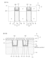
- FIG. 1 is a schematic cross-sectional perspective view showing a partial region of a semiconductor device according to a first embodiment of the present disclosure.
- FIG. 2 is a diagram in which the structure on the first main surface of the chip is removed from FIG. 1.
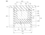
- FIG. 3 is a diagram from FIG. 2 with the emitter contact electrode layer removed.
- FIG. 4 is a schematic plan view of FIG. 3 viewed from the first main surface of the chip.
- FIG. 5 is a sectional view taken along the line VV shown in FIG. 4.
- FIG. 6 is a cross-sectional view taken along line VI-VI shown in FIG. 4.
- 7 is a cross-sectional perspective view taken along line VII-VII shown in FIG. 3.
- FIG. FIG. 8 is a cross-sectional view taken along line VIII-VIII shown in FIG. 4.
- FIG. 9 is an enlarged view of the portion surrounded by the two-dot chain line IX in FIG.
- FIGS. 10A and 10B are diagrams showing a part of the manufacturing process of the semiconductor device.
- FIGS. 11A and 11B are diagrams showing steps after FIGS. 10A and 10B, respectively.
- FIGS. 12A and 12B are diagrams showing steps after FIGS. 11A and 11B, respectively.
- FIGS. 13A and 13B are diagrams showing steps after FIGS. 12A and 12B, respectively.
- FIGS. 14A and 14B are diagrams showing steps after FIGS. 13A and 13B, respectively.
- FIGS. 15A and 15B are diagrams showing steps after FIGS. 14A and 14B, respectively.
- FIGS. 16A and 16B are diagrams showing steps after FIGS. 15A and 15B, respectively.
- FIGS. 17A and 17B are diagrams showing steps after FIGS. 16A and 16B, respectively.
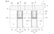
- FIG. 18 is a schematic cross-sectional view showing a partial region of a semiconductor device according to a second embodiment of the present disclosure.
- FIG. 19 is a schematic cross-sectional view showing a partial region of a semiconductor device according to a second embodiment of the present disclosure.
- FIG. 20 is a schematic cross-sectional view showing a partial region of a semiconductor device according to a second embodiment of the present disclosure.
- FIG. 21 is a schematic cross-sectional perspective view showing a partial region of a semiconductor device according to a third embodiment of the present disclosure.
- FIG. 22 is a schematic cross-sectional perspective view showing a partial region of a semiconductor device according to a fourth embodiment of the present disclosure.
- FIG. 23 is a diagram illustrating the steps involved in forming the structure of FIG. 22.
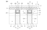
- FIG. 1 is a schematic cross-sectional perspective view showing a partial region of a semiconductor device 1 according to a first embodiment of the present disclosure.
- FIG. 2 is a diagram in which the structure on the first main surface 3 of the chip 2 is removed from FIG. 1.
- FIG. 3 is a diagram from FIG. 2 with the emitter contact electrode layer 51 removed.
- FIG. 4 is a schematic plan view of FIG. 3 viewed from the first main surface 3 of the chip 2.
- FIG. 5 is a sectional view taken along the line VV shown in FIG. 4.
- FIG. 6 is a cross-sectional view taken along line VI-VI shown in FIG. 4.
- 7 is a cross-sectional perspective view taken along line VII-VII shown in FIG. 3.
- FIG. 8 is a cross-sectional view taken along line VIII-VIII shown in FIG. 4.
- FIG. 9 is an enlarged view of the portion surrounded by the two-dot chain line IX in FIG. 5, 6 and 8 also illustrate the structure on the first main surface 3 of the chip 2.
- the semiconductor device 1 has a basic configuration including a trench gate type IGBT (Insulated Gate Bipolar Transistor).
- semiconductor device 1 includes an n ⁇ type chip 2.
- the chip 2 is made of an n - type silicon single crystal substrate.
- the silicon single crystal substrate is formed using an n - type silicon single crystal semiconductor wafer manufactured through the FZ (Floating Zone) method.
- the chip 2 may be called a semiconductor chip or a semiconductor layer.
- the chip 2 has a first main surface 3 on one side and a second main surface 4 on the other side.
- the thickness of the chip 2 may be 50 ⁇ m or more and 300 ⁇ m or less.
- the thickness of the chip 2 may be 50 ⁇ m or more and 100 ⁇ m or less, 100 ⁇ m or more and 150 ⁇ m or less, 150 ⁇ m or more and 200 ⁇ m or less, 200 ⁇ m or more and 250 ⁇ m or less, or 250 ⁇ m or more and 300 ⁇ m or less.
- a p-type collector region 5 is formed on the surface portion of the second main surface 4.
- An n-type charge storage region 6 is formed in the surface portion of the first main surface 3 .
- the charge storage region 6 is formed at a distance from the collector region 5 on the first main surface 3 side.
- an n ⁇ type drift region 7 is formed in a region between a collector region 5 and a charge storage region 6 in chip 2. As shown in FIG. Drift region 7 is formed by a region located between collector region 5 and charge storage region 6 in chip 2 . A p-type body region 8 is formed on the surface of the charge storage region 6 . A plurality of trench gate electrode structures 10 and a plurality of trench emitter electrode structures 11 are formed at intervals on the surface portion of the first main surface 3.
- FIGS. 1 to 7 only one trench gate electrode structure 10 and one trench emitter electrode structure 11 adjacent to each other are shown.
- the structure of the semiconductor device 1 will be described below, focusing on the structure of one trench gate electrode structure 10 and one trench emitter electrode structure 11.
- the trench gate electrode structure 10 and the trench emitter electrode structure 11 extend in a band shape along an arbitrary first direction X in plan view.
- the trench gate electrode structure 10 and the trench emitter electrode structure 11 are formed at intervals along a second direction Y that intersects the first direction X.
- planar view refers to a planar view seen from the normal direction Z of the first principal surface 3 (hereinafter simply referred to as "normal direction Z"). More specifically, the second direction Y is a direction perpendicular to the first direction X. The first direction X and the second direction Y are also tangential directions of the first main surface 3.
- the trench pitch P0 between the trench gate electrode structure 10 and the trench emitter electrode structure 11 may be 0.1 ⁇ m or more and less than 0.6 ⁇ m.
- Trench pitch P0 is 0.1 ⁇ m or more and 0.2 ⁇ m or less, 0.2 ⁇ m or more and 0.3 ⁇ m or less, 0.3 ⁇ m or more and 0.4 ⁇ m or less, 0.4 ⁇ m or more and 0.5 ⁇ m or less, or 0.5 ⁇ m or more and 0.6 ⁇ m It may be less than
- the trench pitch P0 is preferably 0.2 ⁇ m or more and 0.4 ⁇ m or less (for example, about 0.25 ⁇ m).
- the trench gate electrode structure 10 includes a gate trench 12, a gate insulating layer 13, a gate electrode layer 14, a plurality of gate electrode recesses 15, a plurality of gate covering insulating layers 16, a plurality of gate buried bodies 9, and a plurality of gate intermediate insulating layers 22. including.
- Gate trench 12 extends from first main surface 3 through body region 8 and charge storage region 6 to drift region 7 .
- the depth of the gate trench 12 may be 2.0 ⁇ m or more and 4.0 ⁇ m or less.
- the depth of the gate trench 12 may be 2.0 ⁇ m or more and 2.5 ⁇ m or less, 2.5 ⁇ m or more and 3.0 ⁇ m or less, 3.0 ⁇ m or more and 3.5 ⁇ m or less, or 3.5 ⁇ m or more and 4.0 ⁇ m or less.
- the depth of the gate trench 12 is preferably 2.5 ⁇ m or more and 3.5 ⁇ m or less (for example, about 3.0 ⁇ m).
- the width of the gate trench 12 in the second direction may be 0.5 ⁇ m or more and 1.5 ⁇ m or less.
- the width of the gate trench 12 in the second direction is 0.5 ⁇ m or more and 0.75 ⁇ m or less, 0.75 ⁇ m or more and 1.0 ⁇ m or less, 1.0 ⁇ m or more and 1.25 ⁇ m or less, or 1.25 ⁇ m or more and 1.5 ⁇ m or less. Good too.
- the width of the gate trench 12 in the second direction is preferably 0.5 ⁇ m or more and 1.0 ⁇ m or less (for example, about 0.75 ⁇ m).
- the gate insulating layer 13 may be formed of silicon oxide.
- the gate insulating layer 13 is formed in a film shape along the inner wall of the gate trench 12 .
- Gate insulating layer 13 defines a concave space within gate trench 12 .
- the gate electrode layer 14 may be formed of conductive polysilicon. Gate electrode layer 14 is controlled by gate voltage. The gate electrode layer 14 is embedded in the gate trench 12 with the gate insulating layer 13 in between. More specifically, the gate electrode layer 14 is embedded in a concave space defined by the gate insulating layer 13 within the gate trench 12 .
- the plurality of gate electrode recesses 15 are formed on the upper surface of the gate electrode layer 14 at intervals along the first direction X.
- the upper end portion of the gate electrode layer 14 has an uneven structure including a plurality of gate electrode recesses 15.
- the interval between the plurality of gate electrode recesses 15 adjacent to each other may be greater than 0 ⁇ m and less than or equal to 10 ⁇ m.
- the interval between the plurality of gate electrode recesses 15 adjacent to each other is also the width in the first direction X of a portion of the gate electrode layer 14 sandwiched between two gate electrode recesses 15 adjacent to each other.
- the interval between the plurality of gate electrode recesses 15 adjacent to each other may be more than 0 ⁇ m and less than 2 ⁇ m, more than 2 ⁇ m and less than 4 ⁇ m, more than 4 ⁇ m and less than 6 ⁇ m, more than 6 ⁇ m and less than 8 ⁇ m, or more than 8 ⁇ m and less than 10 ⁇ m.
- each gate electrode recess 15 are formed by the gate insulating layer 13 and the gate electrode layer 14.
- a pair of side walls facing each other in the first direction X are formed of the gate electrode layer 14, and a pair of side walls facing each other in the second direction Y are formed of the gate insulating layer 13.
- the bottom wall of each gate electrode recess 15 is formed by the gate electrode layer 14. Referring to FIG. 8, the bottom wall of each gate electrode recess 15 may be located in a region between the first main surface 3 and the bottom of an emitter region 25 (described later) with respect to the normal direction Z, or It may be located deeper than the bottom of the emitter region 25.
- each gate electrode recess 15 is formed in a tapered shape with a bottom area smaller than the opening area.
- the angle ⁇ formed by the upper surface of the gate electrode layer 14 and the side wall of the gate electrode recess 15 within the gate electrode layer 14 may be more than 90° and less than or equal to 120° (for example, about 102°).
- a plurality of gate covering insulating layers 16 are formed within the gate trench 12 on the upper surface of the gate electrode layer 14 and on the sidewalls of the gate electrode recess 15. More specifically, the plurality of gate covering insulating layers 16 are formed independently in the plurality of gate electrode recesses 15. Each gate covering insulating layer 16 covers the gate electrode layer 14 within the gate trench 12, is formed along the sidewall of the gate electrode recess 15, and is exposed from the opening of the gate trench 12. Each gate covering insulating layer 16 defines a concave space in each gate electrode concave portion 15 . The concave space within the gate electrode recess 15 is surrounded by a gate covering insulating layer 16 from below and from the sides.
- gate covering insulating layer 16 includes a bottom portion 23 that covers the upper surface of gate electrode layer 14, and a side portion 24 that extends upward from bottom portion 23 along the sidewall of gate trench 12.
- the bottom portion 23 of the gate covering insulating layer 16 has a thickness of 150 nm or more and 300 nm or less.
- the side portion 24 of the gate covering insulating layer 16 has a first thickness T1 at a lower end portion 47 in the depth direction of the gate trench 12, and has a first thickness T1 at an upper end portion 48 in the depth direction of the gate trench 12. It has a second thickness T2 that is thinner than the thickness T1.
- the first thickness T1 is, for example, 300 nm or less, and the second thickness T2 is, for example, 50 nm or less. Further, the width W1 of the upper end of the gate buried body 9 may be narrower than the width W2 of the upper end of the gate electrode layer 14.
- an outer side surface 29 on the side closer to the side wall of the gate trench 12 and an inner side surface 30 on the opposite side to the outer side surface 29 are located at the lower end of the gate covering insulating layer 16 . They have a tapered shape that slopes closer to each other from 47 toward the upper end 48.
- a step S may be formed between the upper end of the side portion 24 of the gate covering insulating layer 16 and the first main surface 3. In other words, the upper end of the side portion 24 of the gate covering insulating layer 16 may be located at a lower height position with respect to the first main surface 3 in the depth direction of the gate trench 12.
- the plurality of gate embedded bodies 9 may be formed of the same material as the gate electrode layer 14. That is, the plurality of gate buried bodies 9 may be formed of conductive polysilicon. Although the gate buried body 9 has conductivity, it may be electrically floating in this embodiment.
- the gate buried body 9 is buried in the gate electrode recess 15 with the gate covering insulating layer 16 in between. More specifically, the gate buried body 9 is buried in a concave space defined by the gate covering insulating layer 16 in the gate electrode concave portion 15 .
- the plurality of gate intermediate insulating layers 22 may be formed of silicon oxide. Each gate intermediate insulating layer 22 is interposed between the gate electrode layer 14 and the gate covering insulating layer 16 within each gate electrode recess 15 . Referring to FIG. 9, gate intermediate insulating layer 22 is formed between the upper surface of gate electrode layer 14 and the bottom portion 23 of gate covering insulating layer 16 in this embodiment.
- the thickness of the gate intermediate insulating layer 22 (third thickness T3) may be, for example, 20 nm or more and 150 nm or less.
- the gate intermediate insulating layer 22 is clearly distinguished from the gate covering insulating layer 16 (bottom portion 23) in the figure. Depending on the conditions of the manufacturing process, it may not be distinguished from the gate covering insulating layer 16 and may be integrated with the gate covering insulating layer 16 in appearance.
- the trench emitter electrode structure 11 includes an emitter trench 17, an emitter insulating layer 18, an emitter electrode layer 19, an emitter electrode recess 20, an emitter covering insulating layer 21, an emitter buried body 27, and an emitter intermediate insulating layer 28.
- Emitter trench 17 extends from first main surface 3 through body region 8 and charge storage region 6 to drift region 7 .
- the depth of the emitter trench 17 may be 2.0 ⁇ m or more and 4.0 ⁇ m or less.
- the depth of the emitter trench 17 may be 2.0 ⁇ m or more and 2.5 ⁇ m or less, 2.5 ⁇ m or more and 3.0 ⁇ m or less, 3.0 ⁇ m or more and 3.5 ⁇ m or less, or 3.5 ⁇ m or more and 4.0 ⁇ m or less.
- the depth of the emitter trench 17 is preferably 2.5 ⁇ m or more and 3.5 ⁇ m or less (for example, about 3.0 ⁇ m).
- the depth of emitter trench 17 is approximately equal to the depth of gate trench 12.
- the width of the emitter trench 17 in the second direction may be 0.5 ⁇ m or more and 1.5 ⁇ m or less.
- the width in the second direction of the emitter trench 17 is 0.5 ⁇ m or more and 0.75 ⁇ m or less, 0.75 ⁇ m or more and 1.0 ⁇ m or less, 1.0 ⁇ m or more and 1.25 ⁇ m or less, or 1.25 ⁇ m or more and 1.5 ⁇ m or less.
- the width of the emitter trench 17 in the second direction is preferably 0.5 ⁇ m or more and 1.0 ⁇ m or less (for example, about 0.75 ⁇ m).
- the width of the emitter trench 17 in the second direction is preferably approximately equal to the width of the gate trench 12 in the second direction.
- the emitter insulating layer 18 may be formed of silicon oxide. Emitter insulating layer 18 is formed in a film shape along the inner wall of emitter trench 17 . Emitter insulating layer 18 defines a concave space within emitter trench 17 .
- the emitter electrode layer 19 may be formed of conductive polysilicon. Emitter electrode layer 19 is controlled by emitter voltage. The emitter voltage has a voltage value less than the gate voltage. The emitter voltage may be a reference voltage (eg, ground voltage). Emitter electrode layer 19 is embedded in emitter trench 17 with emitter insulating layer 18 in between. More specifically, the emitter electrode layer 19 is embedded in a concave space defined by the emitter insulating layer 18 in the emitter trench 17 .
- the emitter electrode recess 20 is formed so as to dig down almost the entire upper surface of the emitter electrode layer 19. In other words, the emitter electrode layer 19 is buried halfway in the depth direction of the concave space defined by the emitter insulating layer 18 .
- the side walls of the emitter electrode recess 20 are formed by the emitter insulating layer 18 in this embodiment.
- the bottom wall of the emitter electrode recess 20 is formed by the emitter electrode layer 19.
- the bottom wall of the emitter electrode recess 20 may be located in a region between the first main surface 3 and the bottom of the emitter region 25 (described later) with respect to the normal direction Z. However, it may be located deeper than the bottom of the emitter region 25. That is, the upper end of the emitter electrode layer 19 is located on the first main surface 3 side with respect to the bottom of the emitter region 25 (described later). With respect to the normal direction Z, the depth of the emitter electrode recess 20 may be approximately equal to the depth of the gate electrode recess 15.
- the emitter covering insulating layer 21 is formed on the upper surface of the emitter electrode layer 19 and the sidewall of the emitter electrode recess 20 in the emitter trench 17 . That is, the emitter covering insulating layer 21 is formed along the inner wall of the emitter electrode recess 20. The emitter covering insulating layer 21 covers the emitter electrode layer 19 within the emitter trench 17 , is formed along the sidewall of the emitter electrode recess 20 , and is exposed from the opening of the emitter trench 17 . The emitter covering insulating layer 21 defines a concave space in the emitter electrode concave portion 20 . The concave space within the emitter electrode recess 20 is surrounded by an emitter covering insulating layer 21 from below and from the sides. Although the description will be omitted, the emitter covering insulating layer 21 has the same cross-sectional shape as the gate covering insulating layer 16 shown in FIG.
- the emitter buried body 27 may be formed of the same material as the emitter electrode layer 19. That is, the emitter buried body 27 may be formed of conductive polysilicon.
- the emitter embedding body 27 is electrically conductive, but may be electrically floating in this embodiment.
- the emitter embedding body 27 is embedded in the emitter electrode recess 20 with the emitter covering insulating layer 21 in between. More specifically, the emitter embedding body 27 is embedded in a concave space defined by the emitter coating insulating layer 21 within the emitter electrode concave portion 20 .
- the emitter intermediate insulating layer 28 may be formed of silicon oxide.
- the emitter intermediate insulating layer 28 is interposed between the emitter electrode layer 19 and the emitter covering insulating layer 21 within the emitter electrode recess 20 .
- n + type emitter region 25 (impurity region) is formed in a region along the sidewall of the gate trench 12 in the surface portion of the body region 8 . More specifically, a plurality of emitter regions 25 are formed along one sidewall and the other sidewall of the gate trench 12 in the first direction X. The plurality of emitter regions 25 are each formed in a band shape extending along the first direction X. Emitter region 25 is in contact with the sidewall of gate trench 12 . Emitter region 25 is also in contact with the sidewall of emitter trench 17 .
- an emitter region 25 In the region along the sidewall of the gate trench 12 in the surface portion of the first main surface 3, from the first main surface 3 toward the second main surface 4 side, there is an emitter region 25, a body region 8, a charge storage region 6, and a drift region. Regions 7 are formed in this order.
- An IGBT channel CH is formed in the body region 8 in a region facing the gate electrode layer 14 with the gate insulating layer 13 in between.
- a plurality of contact trenches 31 are formed in the surface portion of first main surface 3. As shown in FIG. The plurality of contact trenches 31 are formed at intervals along the first direction X. The plurality of contact trenches 31 are each formed in a band shape extending along the second direction Y. The width of each contact trench 31 in the first direction is smaller than the width of the gate trench 12 in the second direction.
- each contact trench 31 extends from the inner region of the corresponding gate covering insulating layer 16 through the side wall of the gate trench 12 to the surface portion of the first main surface 3.
- each contact trench 31 passes through one sidewall and the other sidewall of the gate trench 12 from the inner region of the gate covering insulating layer 16 in the second direction Y.
- Each contact trench 31 includes a first intersection region 33 that intersects with the gate electrode layer 14 in plan view.
- the bottom wall of each contact trench 31 is formed by the gate covering insulating layer 16
- the side wall of each contact trench 31 is formed by the gate filling body 9 .
- Each contact trench 31 includes a second intersection region 34 that intersects with the emitter electrode layer 19 in plan view.
- the bottom wall of each contact trench 31 is formed by the emitter covering insulating layer 21
- the side wall of each contact trench 31 is formed by the emitter buried body 27 .
- Each contact trench 31 further includes a contact region 35 drawn out from the first intersection region 33 to the outside of the gate trench 12 .
- Contact region 35 may be referred to as a connection region that connects first intersection region 33 and second intersection region 34 in a region between gate trench 12 and emitter trench 17 in plan view.
- the bottom wall of each contact trench 31 is formed by body region 8
- the side wall of each contact trench 31 is formed by body region 8 and emitter region 25 . That is, in the contact region 35, the stacked structure of the body region 8 and the emitter region 25 is exposed on the side wall of the contact trench 31.
- Each contact trench 31 further has a drawn-out portion 32 drawn out from one side wall of the emitter trench 17.
- Each lead-out portion 32 penetrates from the surface portion of the first main surface 3 through one side wall of the emitter trench 17 and reaches into the emitter trench 17 .
- the first depth D1 from the first main surface 3 to the upper surface of the gate electrode layer 14 in the first intersection region 33 is shallower than the second depth D2 of the contact trench 31 in the contact region 35. . Therefore, the contact trench 31 has an uneven structure in which the gate electrode layer 14 and the emitter electrode layer 19 selectively protrude in the second direction Y.
- the first depth D1 is 1 ⁇ m or less, preferably 0.5 ⁇ m or more and 1 ⁇ m or less.
- the second depth D2 is 0.3 ⁇ m or more and 1.0 ⁇ m or less.
- the upper end of the gate electrode layer 14 is located on the first main surface 3 side with respect to the bottom of the emitter region 25.
- the gate electrode layer 14 has opposing portions 40 that face the emitter region 25 with the gate insulating layer 13 in between, near both sides of the first intersection region 33 in the first direction X.
- the opposing portion 40 is a region indicated by horizontal hatching in FIG.
- the opposing portion 40 is located below the pair of gate embedded bodies 9 in the normal direction Z.
- the contact trench 31 includes a first bottom wall 37 in the first intersection region 33 and the second intersection region 34 , and a second bottom wall 38 in the contact region 35 and the lead-out portion 32 .
- a step 39 is formed between the first bottom wall 37 and the second bottom wall 38 due to the difference between the first depth D1 and the second depth D2.
- the arrangement of the plurality of contact trenches 31 is arbitrary.
- the plurality of contact trenches 31 may be formed at equal intervals along the first direction X.
- the plurality of contact trenches 31 may be formed at unequal intervals along the first direction X.
- a p + type contact region 36 is formed in a region along the bottom wall of each contact trench 31 in the body region 8 .
- Contact region 36 may be formed in a region along the bottom wall and side wall of each contact trench 31 in body region 8 .
- the contact region 36 is formed in a region deeper than the emitter region 25 in the body region 8 in the normal direction Z.
- the contact region 36 has an exposed surface exposed from the bottom wall of the contact trench 31.
- the exposed surface of the contact region 36 is formed in a region between the first main surface 3 and the bottom of the body region 8 . More specifically, the exposed surface of the contact region 36 is formed in a region between the bottom of the body region 8 and the bottom of the emitter region 25. More specifically, the exposed surface of the contact region 36 is formed below the upper surface of the gate electrode layer 14 and the upper surface of the emitter electrode layer 19.
- Interlayer insulating layer 41 is formed on the first main surface 3.
- Interlayer insulating layer 41 covers trench gate electrode structure 10 and trench emitter electrode structure 11 .
- Interlayer insulating layer 41 covers gate covering insulating layer 16 and gate buried body 9 exposed from gate trench 12, and emitter covering insulating layer 21 and emitter buried body 27 exposed from emitter trench 17.
- Interlayer insulating layer 41 may be formed of silicon oxide or silicon nitride.
- the interlayer insulating layer 41 may have a laminated structure including an oxide film (SiO 2 film) and a nitride film (SiN film).
- the oxide film (SiO 2 film) may include an NSG (Nondoped Silicon Glass) film that does not contain impurities and/or a PSG (Phosphorus Silicon Glass) film that contains phosphorus.
- the interlayer insulating layer 41 may have a stacked structure including an NSG film and a PSG film stacked in this order from the first main surface 3.
- the thickness of the NSG film may be greater than or equal to 2000 ⁇ and less than or equal to 8000 ⁇ (for example, approximately 5000 ⁇ ).
- the thickness of the PSG film may be greater than or equal to 2000 ⁇ and less than or equal to 6000 ⁇ (for example, about 4000 ⁇ ).
- a plurality of contact holes 42 are formed in the interlayer insulating layer 41. Each of the plurality of contact holes 42 communicates with the corresponding contact trench 31 . That is, the plurality of contact holes 42 are formed at intervals along the first direction X, and are each formed in a band shape extending along the second direction Y.
- the plurality of contact holes 42 penetrate the interlayer insulating layer 41 and communicate with the corresponding contact trenches 31, respectively. Thereby, the plurality of contact holes 42 form one emitter contact trench 31, 42 with the corresponding contact trench 31.
- the width of each contact hole 42 in the first direction may be greater than or equal to the width of each contact trench 31 in the first direction. That is, the width of each contact hole 42 in the first direction may be equal to the width of each contact trench 31 in the first direction, or may exceed the width of each contact trench 31 in the first direction.
- the inner wall of each contact hole 42 may surround the inner wall of the corresponding contact trench 31.
- the arrangement of the plurality of contact holes 42 is arbitrary and adjusted according to the arrangement of the contact trenches 31.
- the plurality of contact holes 42 may be formed at equal intervals along the first direction X.
- the plurality of contact holes 42 may be formed at unequal intervals along the first direction X.
- An emitter main surface electrode layer 43 is formed on the interlayer insulating layer 41. Emitter main surface electrode layer 43 enters contact hole 42 and contact trench 31 (that is, emitter contact trenches 31 and 42) from above interlayer insulating layer 41.
- the emitter main surface electrode layer 43 may include, for example, a laminated structure of a barrier layer made of titanium or the like and an electrode layer made of tungsten or the like.
- a plurality of emitter contact electrode layers 51 are formed by portions of the emitter main surface electrode layer 43 located within the plurality of contact trenches 31 . As a result, a structure in which a plurality of emitter contact electrode layers 51 are embedded in the surface portion of the chip 2 is formed.
- the plurality of emitter contact electrode layers 51 each have an arrangement and shape corresponding to the arrangement and shape of the plurality of contact trenches 31. That is, the plurality of emitter contact electrode layers 51 are formed at intervals along the first direction X, and are each formed in a band shape extending along the second direction Y.
- Each emitter contact electrode layer 51 faces the gate electrode layer 14 with the gate covering insulating layer 16 in between with respect to the normal direction Z and the first direction are doing.
- Each emitter contact electrode layer 51 is insulated from gate electrode layer 14 by gate covering insulating layer 16 .
- a gate buried body 9 is interposed between the emitter contact electrode layer 51 and the gate covering insulating layer 16.
- the gate buried bodies 9 are provided on both sides of the first intersection region 33 in the first direction It includes a pair of gate embedded bodies 9 sandwiched from the sides. Therefore, in the first intersection region 33, the emitter contact electrode layer 51 is in direct contact with the gate covering insulating layer 16 in the normal direction Z, and in contact with the gate buried body 9 in the first direction X.
- the emitter contact electrode layer 51 is surrounded from three sides by the lower gate covering insulating layer 16 and the gate filling bodies 9 on both sides.
- Each emitter contact electrode layer 51 faces the emitter electrode layer 19 with the emitter covering insulating layer 21 in between with respect to the normal direction Z and the first direction are doing.
- Each emitter contact electrode layer 51 is insulated from emitter electrode layer 19 by emitter covering insulating layer 21 .
- an emitter buried body 27 is interposed between the emitter contact electrode layer 51 and the emitter covering insulating layer 21.
- the emitter embedded bodies 27 are provided on both sides of the second intersection region 34 in the first direction It includes a pair of emitter embedding bodies 27 which are sandwiched from the sides. Therefore, in the second intersection region 34, the emitter contact electrode layer 51 is in direct contact with the emitter covering insulating layer 21 in the normal direction Z, and in contact with the emitter buried body 27 in the first direction X.
- the emitter contact electrode layer 51 is surrounded from three sides by the emitter covering insulating layer 21 below and the emitter buried bodies 27 on both sides.
- a collector electrode layer 61 is formed on the second main surface 4 of the chip 2. Collector electrode layer 61 is connected to collector region 5 .
- a gate main surface electrode layer having the same structure as the emitter main surface electrode layer 43 may be formed on the interlayer insulating layer 41. The gate main surface electrode layer may be electrically connected to the gate electrode layer 14 through a gate contact hole formed in the interlayer insulating layer 41.
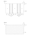
- FIGS. 10A, 10B to 17A, 17B are diagrams showing part of the manufacturing process of the semiconductor device 1 in order of process.
- the drawings marked with “A” correspond to the cross-sections in FIG. 5
- the drawings marked with "B” correspond to the cross-sections in FIG. 8. ing.
- an n ⁇ type semiconductor wafer 26 is prepared.
- the semiconductor wafer 26 has the first main surface 3 and the second main surface 4 (not shown) of the chip 2 described above.
- a p-type collector region 5 (not shown) and an n-type charge storage region 6 are formed in the semiconductor wafer 26.
- Collector region 5 is formed by introducing p-type impurities into second main surface 4 of semiconductor wafer 26 .
- the collector region 5 may be formed on the surface portion of the second main surface 4 of the semiconductor wafer 26 by an ion implantation method using an ion implantation mask (not shown).
- Charge storage region 6 is formed by introducing n-type impurities into first main surface 3 .
- the charge storage region 6 may be formed on the surface portion of the first main surface 3 by an ion implantation method using an ion implantation mask (not shown).
- unnecessary portions of the semiconductor wafer 26 are selectively removed from the first main surface 3 through a mask having a predetermined pattern. Unnecessary portions of the semiconductor wafer 26 may be removed by an etching method (for example, a wet etching method). As a result, gate trench 12 and emitter trench 17 are formed. The mask is then removed. Next, gate insulating layer 13 and emitter insulating layer 18 are formed on the inner walls of gate trench 12 and emitter trench 17, respectively, by thermal oxidation or wet oxidation, for example. Next, gate electrode layer 14 and emitter electrode layer 19 are buried in gate trench 12 and emitter trench 17, respectively, by, for example, the CVD method. As a result, a trench gate electrode structure 10 and a trench emitter electrode structure 11 are formed.
- an etching method for example, a wet etching method
- gate electrode layer 14 and emitter electrode layer 19 are selectively removed from first main surface 3 through a mask having a predetermined pattern. As a result, gate electrode recess 15 and emitter electrode recess 20 are formed.
- the unnecessary portions of the gate electrode layer 14 and the unnecessary portions of the emitter electrode layer 19 may be removed by an etching method (for example, a wet etching method).
- a first base insulating layer 44 will be the base of the gate intermediate insulating layer 22 and the emitter intermediate insulating layer 28, and a first base insulating layer 44 will be the base of the gate covering insulating layer 16 and the emitter covering insulating layer 21.
- a second base insulating layer 45 is formed.
- the first base insulating layer 44 may be formed, for example, by thermal oxidation treatment of the surfaces of the gate electrode layer 14 and emitter electrode layer 19 and the surface of the semiconductor wafer 26.
- the second base insulating layer 45 may be formed by depositing an insulating material on the first base insulating layer 44 by, for example, a CVD method.
- the first base insulating layer 44 and the second base insulating layer 45 are formed in the gate trench 12 and the emitter trench 17, and are also formed to cover the first main surface 3 of the semiconductor wafer 26.
- a polysilicon layer that will become the base of gate buried body 9 and emitter buried body 27 is deposited over the entire first main surface 3 by, for example, the CVD method. Thereafter, the polysilicon layer is planarized by etching back to obtain a gate buried body 9 and an emitter buried body 27 buried in the gate electrode recess 15 and the emitter electrode recess 20, respectively.
- Body region 8 is formed by introducing p-type impurities into first main surface 3 .
- Body region 8 may be formed on the surface portion of first main surface 3 by ion implantation using an ion implantation mask (not shown).
- Emitter region 25 is formed by introducing n-type impurities into first main surface 3 .
- the emitter region 25 may be formed on the surface portion of the first main surface 3 by an ion implantation method using an ion implantation mask (not shown).
- interlayer insulating layer 41 is formed on first main surface 3.
- Interlayer insulating layer 41 is formed on first main surface 3 to cover trench gate electrode structure 10 and trench emitter electrode structure 11 .
- This step may include a step of forming an NSG film (for example, 5000 ⁇ ) and a PSG film (for example, 4000 ⁇ ) on the first main surface 3 in this order by the CVD method.
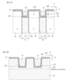
- unnecessary parts of interlayer insulating layer 41, unnecessary parts of gate covering insulating layer 16, and unnecessary parts of emitter covering insulating layer 21 are removed through a mask having a predetermined pattern. Selectively removed. Unnecessary portions such as the interlayer insulating layer 41 may be removed by an etching method (for example, a dry etching method). As a result, a contact hole 42 is formed.
- unnecessary portions of the semiconductor wafer 26 are removed through the mask used when forming the contact holes 42.
- the unnecessary portion of the semiconductor wafer 26 may be removed by, for example, an etching method (for example, a dry etching method).
- a contact trench 31 is formed in the first main surface 3.
- FIG. 16A the structure visible on the back side of the contact trench 31 is shown by broken line hatching.
- the gate buried body 9 is also etched at the same time when the contact trench 31 is formed. Further, the second depth D2 of the contact trench 31 is larger than the thickness T4 of the gate buried body 9 (see FIGS. 15A and 15B). Therefore, in the first intersection region 33 , the gate buried body 9 is etched so that the gate buried body 9 penetrates from the first main surface 3 to the bottom wall of the gate electrode recess 15 .
- a contact region 36 is formed on the surface portion of the first main surface 3. More specifically, contact region 36 is formed in a region along the bottom wall of contact trench 31 in the surface layer portion of body region 8 . Contact region 36 may be formed in a region along the sidewall and bottom wall of contact trench 31. Contact region 36 is formed by introducing p-type impurities into contact trench 31 . Contact region 36 may be introduced into contact trench 31 by ion implantation through an ion implantation mask (not shown). As a result, a contact region 36 along the bottom wall of the contact trench 31 is formed.
- emitter main surface electrode layer 43 is formed on interlayer insulating layer 41.
- the emitter main surface electrode layer 43 may be formed by a sputtering method or a CVD method.
- the emitter contact electrode layer 51 is formed by the portion of the emitter main surface electrode layer 43 that enters the contact trench 31 .
- a collector electrode layer 61 is formed on the second main surface 4 of the semiconductor wafer 26 .
- the gate buried body 9 is formed of polysilicon, and has an etching selectivity with respect to the interlayer insulating layer 41 made of silicon oxide or silicon nitride.
- the gate buried body 9 having an etching selectivity with respect to the interlayer insulating layer 41 means, for example, the etching ratio shown by the ratio of the etching amount (a) of the interlayer insulating layer 41 to the etching amount (b) of the gate buried body 9.
- the selectivity ratio (a/b) is, for example, 1.5 or more, preferably 5 or more, and more preferably 10 or more.
- the gate embedded body 9 can be used as an etching stopper. It is possible to prevent the gate intermediate insulating layer 22 from being exposed to etching gas when forming the contact hole 42. Therefore, the thickness of the gate intermediate insulating layer 22 can be easily controlled to a designed value by the formation conditions of the gate intermediate insulating layer 22 (for example, thermal oxidation conditions, CVD conditions, etc.). Therefore, short circuits between the gate electrode layer 14 and the emitter contact electrode layer 51 and reduction in TZDB (Time Zero Dielectric Breakdown) are prevented, and the controllability of the capacitance between the gate electrode layer 14 and the emitter contact electrode layer 51 is improved. can be improved.
- TZDB Time Zero Dielectric Breakdown
- the gate intermediate insulating layer 22 is not etched when forming the contact hole 42. Therefore, it is not necessary to form the gate intermediate insulating layer 22 excessively thick in order to prevent a short circuit between the gate and the emitter due to over-etching of the gate intermediate insulating layer 22. Furthermore, there is no need to form the gate electrode recess 15 deeply in order to form the thick gate intermediate insulating layer 22. As a result, the gate electrode recess 15 can be formed relatively shallowly, so that the facing portion 40 of the gate electrode layer 14 facing the emitter region 25 with the gate insulating layer 13 interposed in the vicinity of both sides of the first intersection region 33 can be formed relatively shallowly. can be secured.
- a region near the first intersection region 33 can be used as a channel forming region 46 (see FIG. 3), so that reduction in channel width can be suppressed. Therefore, it is possible to provide a semiconductor device 1 that can reduce on-resistance.
- FIG. 18 is a schematic cross-sectional view showing a partial region of a semiconductor device 71 according to a second embodiment of the present disclosure.
- FIG. 19 is a schematic cross-sectional view showing a partial region of a semiconductor device 71 according to a second embodiment of the present disclosure.
- FIG. 20 is a schematic cross-sectional view showing a partial region of the semiconductor device 71 according to the second embodiment of the present disclosure. 18 corresponds to the cross section of FIG. 5, FIG. 19 corresponds to the cross section of FIG. 6, and FIG. 20 corresponds to the cross section of FIG.
- structures corresponding to those described for the semiconductor device 1 according to the first embodiment will be given the same reference numerals and descriptions will be omitted.
- the first depth D1 from the first main surface 3 to the upper surface of the gate electrode layer 14 in the first intersection region 33 is the depth of the contact trench 31 in the contact region 35. is deeper than the second depth D2.
- a stacked structure of the gate covering insulating layer 16 and the gate buried body 9 is formed on the bottom wall of the contact trench 31 .
- the gate buried body 9 is formed so as to span from one side of the first intersection region 33 in the first direction X to the other side, and the emitter contact electrode layer 51 is It surrounds from both sides and from below.
- the upper end of the gate electrode layer 14 is located on the second main surface 4 side (opposite the first main surface 3) with respect to the bottom of the emitter region 25. Therefore, in the semiconductor device 71 according to the second embodiment, the opposing portion 40 shown in FIG. It does not face the emitter region 25 via.
- the semiconductor device 71 according to the second embodiment can also achieve the same effects as those described for the semiconductor device 1.
- the semiconductor device 71 can be manufactured by simply changing the depth of the gate electrode recess 15 and the depth of the emitter electrode recess 20 in the method of manufacturing the semiconductor device 1.
- FIG. 21 is a schematic cross-sectional perspective view showing a partial region of a semiconductor device 81 according to a third embodiment of the present disclosure.
- structures corresponding to those described for the semiconductor device 1 will be given the same reference numerals and descriptions will be omitted.
- the semiconductor device 1 described above an example has been described in which the p-type collector region 5 is formed on the surface portion of the second main surface 4.
- an n-type drain region 82 is formed on the surface of the second main surface 4 instead of the p-type collector region 5 .
- the semiconductor device 81 has a basic configuration including a trench gate type MISFET (Metal Insulator Semiconductor Field Effect Transistor).
- MISFET Metal Insulator Semiconductor Field Effect Transistor
- the semiconductor device 81 can also achieve the same effects as those described for the semiconductor device 1.
- the semiconductor device 81 can be manufactured by simply forming an n-type drain region 82 in place of the p-type collector region 5 and changing the layout of each mask in the method for manufacturing the semiconductor device 1.
- FIG. 22 is a schematic cross-sectional perspective view showing a partial region of a semiconductor device 91 according to a fourth embodiment of the present disclosure.
- FIG. 23 is a diagram illustrating the steps involved in forming the structure of FIG. 22. 22 and 23 show cross sections of the above-described semiconductor device 1 corresponding to FIG. 9. In the following, structures corresponding to those described for the semiconductor device 1 will be given the same reference numerals and descriptions will be omitted.
- the width W1 of the upper end of the gate buried body 9 is narrower than the width W2 of the upper end of the gate electrode layer 14.
- the width W1 of the upper end of the gate buried body 9 is wider than the width W2 of the upper end of the gate electrode layer 14.
- the gate trench 12 is formed in a tapered shape with a bottom area smaller than an opening area.
- the angle ⁇ 2 formed by the side wall of the gate trench 12 with respect to a plane 92 parallel to the first main surface 3 may be, for example, more than 80° and less than 90°, preferably more than 85° and less than 90°. good. Therefore, in the depth direction of the gate trench 12, the width W1 of the gate buried body 9 formed at a position closer to the open end of the gate trench 12 than the depth position of the gate electrode layer 14 is the width W2 of the gate electrode layer 14. becomes wider than
- the side portion 24 of the gate covering insulating layer 16 has the upper end portion 48 having a second thickness T2 that is thinner than the first thickness T1 of the lower end portion 47.
- the second thickness T2 may be 0 (zero) because the outer side surface 29 and the inner side surface 30 are in contact with each other at the upper end portion 48.
- the upper end portion 48 of the side portion 24 of the gate covering insulating layer 16 may be a sharp tip pointing upward.
- the semiconductor device 91 can also achieve the same effects as those described for the semiconductor device 1.
- the semiconductor device 91 is manufactured in the method for manufacturing the semiconductor device 1 by forming the gate trench 12 by etching to form a tapered shape and forming the side portions 24 of the gate covering insulating layer 16 so as to have a tapered shape. can.
- the mesa structure 93 of the chip 2 (the part where the emitter region 25 and the like are formed) formed on the side of the gate trench 12 is trapezoidal and round in cross-sectional view. It may have a formed upper end 94.
- the width W1 of the gate buried body 9 can be made wider than the width W2 of the gate electrode layer 14.
- a structure may be adopted in which the conductivity type of each semiconductor portion is inverted. That is, the p-type portion may be made into the n-type, and the n-type portion may be made into the p-type.
- chip 2 is made of silicon single crystal.
- chip 2 may also include SiC.
- the chip 2 may be made of SiC single crystal.
- the gate trench (12) is formed on the first main surface (3) so as to cover the gate electrode (14) and extends along a second direction (Y) intersecting the first direction (X).
- the surface insulating layer (41) having a contact hole (42) drawn out from the upper region to the outside of the gate trench (12); electrically connected to the body region (8) and the first impurity region (25) through the contact hole (42), and from inside the gate trench (12) through the sidewall of the gate trench (12).
- a semiconductor device (1) including a buried body (9) buried in a region above the covering insulating layer (16) in the gate trench (12) and having an etching selectivity with respect to the surface insulating layer (41). , 71, 81).
- the covering insulating layer (16) has a bottom part (23) that covers the upper surface of the gate electrode (14), and a side part (24) that extends upward from the bottom part (23) along the side wall of the gate trench (12). )
- Appendix 1-3 The semiconductor device (1, 71, 81) according to appendix 1-2, wherein the bottom portion (23) of the covering insulating layer (16) has a thickness of 150 nm or more and 300 nm or less.
- the side portion (24) of the covering insulating layer (16) has a first thickness (T1) at a lower end portion (47) in the depth direction of the gate trench (12), and
- the side portion (24) of the covering insulating layer (16) includes an outer side surface (29) on the side closer to the side wall of the gate trench (12) and an inner side surface on the opposite side to the outer side surface (29).
- (30) has a tapered shape that is inclined toward each other from the lower end (47) to the upper end (48), according to any one of Supplementary notes 1-2 to 1-4. (1, 71, 81).
- the body region (8) is formed at least along the bottom wall (37, 38) of the contact trench (31),
- the first impurity region (25) is formed at least along the sidewall of the contact trench (31), Supplementary Note 1, wherein the contact electrode (51) is embedded in the contact trench (31) and connected to the body region (8) and the first impurity region (25) inside the contact trench (31).
- the semiconductor device (1, 71, 81) according to any one of -1 to Supplementary Note 1-5.
- the contact trench (31) has an intersection region (33) that intersects with the gate trench (12), is drawn out from the intersection region (33) to the outside of the gate trench (12), and is connected to the body region (8) and the intersection region (33). a contact region (35) in which the first impurity region (25) is exposed;
- the depth (D1) from the first main surface (3) in the intersection region (33) to the upper surface of the gate electrode (14) is the depth (D1) from the first main surface (3) in the contact region (35) to the top surface of the gate electrode (14).
- the semiconductor device (1, 81) according to appendix 1-6, which is shallower than the depth (D2) to the bottom wall of the contact trench (31).
- the depth (D1) from the first main surface (3) to the upper surface of the gate electrode (14) in the intersection region (33) is 1 ⁇ m or less, according to Appendix 1-7 or 1-8.
- the contact trench (31) has an intersection region (33) that intersects with the gate trench (12), is drawn out from the intersection region (33) to the outside of the gate trench (12), and is connected to the body region (8) and the intersection region (33). a contact region in which the first impurity region (25) is exposed;
- the depth (D1) from the first main surface (3) in the intersection region (33) to the upper surface of the gate electrode (14) is the depth (D1) from the first main surface (3) in the contact region to the contact trench (
- the semiconductor device (71) according to appendix 1-6 which is deeper than the depth (D2) to the bottom wall of 31).
- the bottom wall (37) of the contact trench (31) is formed with a laminated structure of the bottom (23) of the covering insulating layer (16) and the embedded body (9).
- the embedded body (9) is formed so as to span from one side to the other side of the intersection region (33) in the first direction (X), and connects the contact electrode (51) with the intersection region (33) in the first direction (X).
- the semiconductor device (71) according to appendix 1-10 which is surrounded from both sides and from three directions below.
- the surface insulating layer (41) is made of silicon oxide, The semiconductor device (1, 71, 81) according to any one of attachments 1-1 to 1-12, wherein the gate electrode (14) and the buried body (9) are formed of polysilicon.
- a contact trench (31) is formed in the surface portion of the first main surface (3) so that the body region (8) and the first impurity region (25) are exposed by etching through the contact hole (42). a step of forming; forming a contact electrode (51) connected to the body region (8) and the first impurity so as to be embedded in the contact trench (31), The method for manufacturing a semiconductor device (1, 71, 81), wherein the embedded body (9) is formed of a material having an etching selectivity with respect to the surface insulating layer (41).
Landscapes
- Electrodes Of Semiconductors (AREA)
Priority Applications (3)
| Application Number | Priority Date | Filing Date | Title |
|---|---|---|---|
| CN202380064460.8A CN119856588A (zh) | 2022-09-09 | 2023-08-28 | 半导体装置以及半导体装置的制造方法 |
| JP2024545580A JPWO2024053456A1 (https=) | 2022-09-09 | 2023-08-28 | |
| US19/073,075 US20250203897A1 (en) | 2022-09-09 | 2025-03-07 | Semiconductor device and method for manufacturing semiconductor device |
Applications Claiming Priority (2)
| Application Number | Priority Date | Filing Date | Title |
|---|---|---|---|
| JP2022-143915 | 2022-09-09 | ||
| JP2022143915 | 2022-09-09 |
Related Child Applications (1)
| Application Number | Title | Priority Date | Filing Date |
|---|---|---|---|
| US19/073,075 Continuation US20250203897A1 (en) | 2022-09-09 | 2025-03-07 | Semiconductor device and method for manufacturing semiconductor device |
Publications (1)
| Publication Number | Publication Date |
|---|---|
| WO2024053456A1 true WO2024053456A1 (ja) | 2024-03-14 |
Family
ID=90191233
Family Applications (1)
| Application Number | Title | Priority Date | Filing Date |
|---|---|---|---|
| PCT/JP2023/030989 Ceased WO2024053456A1 (ja) | 2022-09-09 | 2023-08-28 | 半導体装置および半導体装置の製造方法 |
Country Status (4)
| Country | Link |
|---|---|
| US (1) | US20250203897A1 (https=) |
| JP (1) | JPWO2024053456A1 (https=) |
| CN (1) | CN119856588A (https=) |
| WO (1) | WO2024053456A1 (https=) |
Citations (5)
| Publication number | Priority date | Publication date | Assignee | Title |
|---|---|---|---|---|
| JP2001160549A (ja) * | 1999-12-03 | 2001-06-12 | Matsushita Electronics Industry Corp | ドライエッチング方法 |
| JP2003303967A (ja) * | 2002-04-09 | 2003-10-24 | Shindengen Electric Mfg Co Ltd | 半導体装置およびその製造方法 |
| JP2005116985A (ja) * | 2003-10-10 | 2005-04-28 | Toyota Motor Corp | トレンチゲート型半導体装置 |
| WO2019103135A1 (ja) * | 2017-11-24 | 2019-05-31 | ローム株式会社 | 半導体装置 |
| JP2019220727A (ja) * | 2019-10-07 | 2019-12-26 | ローム株式会社 | 半導体装置 |
-
2023
- 2023-08-28 CN CN202380064460.8A patent/CN119856588A/zh active Pending
- 2023-08-28 WO PCT/JP2023/030989 patent/WO2024053456A1/ja not_active Ceased
- 2023-08-28 JP JP2024545580A patent/JPWO2024053456A1/ja active Pending
-
2025
- 2025-03-07 US US19/073,075 patent/US20250203897A1/en active Pending
Patent Citations (5)
| Publication number | Priority date | Publication date | Assignee | Title |
|---|---|---|---|---|
| JP2001160549A (ja) * | 1999-12-03 | 2001-06-12 | Matsushita Electronics Industry Corp | ドライエッチング方法 |
| JP2003303967A (ja) * | 2002-04-09 | 2003-10-24 | Shindengen Electric Mfg Co Ltd | 半導体装置およびその製造方法 |
| JP2005116985A (ja) * | 2003-10-10 | 2005-04-28 | Toyota Motor Corp | トレンチゲート型半導体装置 |
| WO2019103135A1 (ja) * | 2017-11-24 | 2019-05-31 | ローム株式会社 | 半導体装置 |
| JP2019220727A (ja) * | 2019-10-07 | 2019-12-26 | ローム株式会社 | 半導体装置 |
Also Published As
| Publication number | Publication date |
|---|---|
| US20250203897A1 (en) | 2025-06-19 |
| CN119856588A (zh) | 2025-04-18 |
| JPWO2024053456A1 (https=) | 2024-03-14 |
Similar Documents
| Publication | Publication Date | Title |
|---|---|---|
| US20220131000A1 (en) | Shielded gate trench mosfet devices | |
| CN107112358B (zh) | 半导体装置及半导体装置的制造方法 | |
| US8952430B2 (en) | Semiconductor device and method for manufacturing semiconductor device | |
| JP4754353B2 (ja) | 縦型トレンチゲート半導体装置およびその製造方法 | |
| US9614073B2 (en) | Semiconductor device, and manufacturing method for same | |
| US6455378B1 (en) | Method of manufacturing a trench gate power transistor with a thick bottom insulator | |
| JP6666671B2 (ja) | 半導体装置 | |
| CN101299436A (zh) | 应用hdp淀积的源-体注入阻挡块的器件结构及制造方法 | |
| US20190006496A1 (en) | Semiconductor device and method of manufacturing the same | |
| CN108695390B (zh) | 半导体器件及其制造方法 | |
| CN113224133B (zh) | 多栅极变化的场效晶体管结构及其制造方法、芯片装置 | |
| JP2005268679A (ja) | 半導体装置およびその製造方法 | |
| JP3965027B2 (ja) | トレンチ底部に厚いポリシリコン絶縁層を有するトレンチゲート型misデバイスの製造方法 | |
| TW202501578A (zh) | 半導體裝置 | |
| JP4735235B2 (ja) | 絶縁ゲート型半導体装置およびその製造方法 | |
| JP4623656B2 (ja) | 縦型ゲート半導体装置およびその製造方法 | |
| WO2024053456A1 (ja) | 半導体装置および半導体装置の製造方法 | |
| JP2024170183A (ja) | 半導体装置およびその製造方法 | |
| US20250203898A1 (en) | Semiconductor device | |
| JP7821705B2 (ja) | 半導体装置の製造方法 | |
| US20240304682A1 (en) | Semiconductor device and method of manufacturing semiconductor device | |
| JP2023162780A (ja) | 半導体装置 | |
| JPWO2025173150A5 (https=) | ||
| JP2025011470A (ja) | 半導体装置 | |
| CN119789482A (zh) | 半导体器件及其制造方法 |
Legal Events
| Date | Code | Title | Description |
|---|---|---|---|
| 121 | Ep: the epo has been informed by wipo that ep was designated in this application |
Ref document number: 23862995 Country of ref document: EP Kind code of ref document: A1 |
|
| WWE | Wipo information: entry into national phase |
Ref document number: 2024545580 Country of ref document: JP |
|
| WWE | Wipo information: entry into national phase |
Ref document number: 202380064460.8 Country of ref document: CN |
|
| NENP | Non-entry into the national phase |
Ref country code: DE |
|
| WWP | Wipo information: published in national office |
Ref document number: 202380064460.8 Country of ref document: CN |
|
| 122 | Ep: pct application non-entry in european phase |
Ref document number: 23862995 Country of ref document: EP Kind code of ref document: A1 |