WO2024053267A1 - 半導体装置 - Google Patents
半導体装置 Download PDFInfo
- Publication number
- WO2024053267A1 WO2024053267A1 PCT/JP2023/026844 JP2023026844W WO2024053267A1 WO 2024053267 A1 WO2024053267 A1 WO 2024053267A1 JP 2023026844 W JP2023026844 W JP 2023026844W WO 2024053267 A1 WO2024053267 A1 WO 2024053267A1
- Authority
- WO
- WIPO (PCT)
- Prior art keywords
- trenches
- semiconductor device
- field plate
- trench
- semiconductor
- Prior art date
- Legal status (The legal status is an assumption and is not a legal conclusion. Google has not performed a legal analysis and makes no representation as to the accuracy of the status listed.)
- Ceased
Links
Images


Classifications
-
- H—ELECTRICITY
- H10—SEMICONDUCTOR DEVICES; ELECTRIC SOLID-STATE DEVICES NOT OTHERWISE PROVIDED FOR
- H10D—INORGANIC ELECTRIC SEMICONDUCTOR DEVICES
- H10D62/00—Semiconductor bodies, or regions thereof, of devices having potential barriers
- H10D62/10—Shapes, relative sizes or dispositions of the regions of the semiconductor bodies; Shapes of the semiconductor bodies
-
- H—ELECTRICITY
- H10—SEMICONDUCTOR DEVICES; ELECTRIC SOLID-STATE DEVICES NOT OTHERWISE PROVIDED FOR
- H10D—INORGANIC ELECTRIC SEMICONDUCTOR DEVICES
- H10D30/00—Field-effect transistors [FET]
- H10D30/60—Insulated-gate field-effect transistors [IGFET]
Definitions
- the present disclosure relates to a semiconductor device.
- Patent Document 1 discloses a semiconductor device having a plurality of trench gate structures formed in a stripe shape. Each trench gate structure includes a gate trench and two electrodes buried separately in the depth direction of the gate trench.
- the gate electrode and the field plate electrode When the gate electrode and the field plate electrode are buried separately in the gate trench, the gate electrode and the field plate electrode extend into the gate trench while facing each other. If the capacitance created by the gate electrode and the field plate electrode is relatively large, undesirable behavior of the semiconductor device, such as self-turn-on, can be caused.
- a semiconductor device includes a semiconductor layer, a plurality of first trenches formed in the semiconductor layer and arranged in a mesh shape, and extending in a first direction in a plan view; a plurality of second trenches extending in a second direction intersecting the first direction when viewed, the plurality of first trenches and the plurality of second trenches intersecting and communicating with each other; an insulating layer formed on the semiconductor layer; a plurality of gate electrodes each embedded in the plurality of first trenches via the insulating layer and extending in the first direction; and a plurality of second trenches.
- a plurality of field plate electrodes are respectively embedded in the trenches via the insulating layer and extend in the second direction.
- the capacitance caused by the gate electrode and the field plate electrode can be reduced.
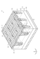
- FIG. 1 is a schematic cross-sectional perspective view of an exemplary semiconductor device according to one embodiment.
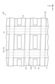
- FIG. 2 is a schematic plan view of the semiconductor device shown in FIG. 1.
- FIG. 3 is a schematic cross-sectional view of the semiconductor device taken along line F3-F3 in FIG.
- FIG. 4 is a schematic cross-sectional view of the semiconductor device taken along line F4-F4 in FIG.
- FIG. 5 is a schematic cross-sectional view of the semiconductor device taken along line F5-F5 in FIG.
- FIG. 6 is a schematic cross-sectional view of the semiconductor device taken along line F6-F6 in FIG.
- FIG. 7 is a schematic cross-sectional perspective view of an exemplary semiconductor device according to a comparative example.
- FIG. 8 is a schematic cross-sectional view of the semiconductor device shown in FIG. 7.
- FIG. 9 is a schematic plan view of a semiconductor device according to a modification example.
- FIG. 1 is a schematic cross-sectional perspective view of an exemplary semiconductor device 10 according to one embodiment.
- FIG. 2 is a schematic plan view of the semiconductor device 10.
- the semiconductor device 10 may be, for example, a MISFET (Metal-Insulator-Semiconductor Field Effect Transistor) having a trench gate structure.
- the semiconductor device 10 includes a semiconductor layer 12 , a cell trench 14 formed in the semiconductor layer 12 , and an insulating layer 16 formed on the semiconductor layer 12 .
- the semiconductor layer 12 may include a semiconductor substrate 18 and an epitaxial layer 20, and the cell trench 14 may be formed in the epitaxial layer 20.
- the semiconductor substrate 18 may be a silicon (Si) substrate.
- the epitaxial layer 20 may be a Si epitaxial layer.
- the top surface 12A of the semiconductor layer 12 may be included in the epitaxial layer 20, while the bottom surface 12B of the semiconductor layer 12 may be included in the semiconductor substrate 18.
- Insulating layer 16 may include at least one of a silicon oxide (SiO 2 ) layer and a silicon nitride (SiN) layer.
- a cross-sectional view and a plan view of the semiconductor device 10 at the position of the upper surface 12A of the semiconductor layer 12 are shown, respectively, for ease of understanding (line F1-F1 in FIG. 3). reference). It should be noted that, as shown in FIG. 3, the insulating layer 16 is formed not only within the cell trench 14 but also on the upper surface 12A of the semiconductor layer 12.
- the semiconductor device 10 may further include a drain electrode 22 formed on the bottom surface 12B of the semiconductor layer 12.
- Drain electrode 22 may be formed from at least one of titanium (Ti), nickel (Ni), gold (Au), silver (Ag), copper (Cu), Al, Cu alloy, and Al alloy. .
- the cell trench 14 includes a plurality of first trenches 24 extending in a first direction in plan view and a plurality of second trenches extending in a second direction intersecting the first direction in plan view. 26.
- the Z-axis direction of the mutually orthogonal XYZ axes shown in FIGS. 1 and 2 is a direction that is orthogonal to the surface of the semiconductor layer 12.
- the term "planar view” used in this specification refers to viewing the semiconductor device 10 from above along the Z-axis direction, unless explicitly stated otherwise.
- the first direction is the longitudinal direction of the first trench 24, and the second direction is the longitudinal direction of the second trench 26. In the example shown in FIGS.
- the first direction may be the Y-axis direction
- the second direction may be the X-axis direction. Therefore, in the illustrated example, the angle between the first direction and the second direction is 90 degrees. Note that, as will be described later with reference to FIG. 9, the first direction and the second direction do not necessarily have to correspond to the Y-axis direction and the X-axis direction, respectively.
- the cell trench 14 has an opening in the upper surface 12A of the semiconductor layer 12 and has a depth in the Z-axis direction.
- the plurality of first trenches 24 and the plurality of second trenches 26 intersect and communicate with each other. Thereby, the cell trenches 14 are arranged in a mesh shape.
- the cell trench 14 includes a plurality of intersection regions 14A where a plurality of first trenches 24 and a plurality of second trenches 26 intersect with each other, and a plurality of first trenches 24 and a plurality of second trenches 26. and a plurality of non-intersecting regions 14B that do not intersect with each other.
- the plurality of first trenches 24 may be arranged in stripes.
- each of the plurality of first trenches 24 has a width W1.
- the width W1 of the first trench 24 corresponds to the dimension of the first trench 24 in the lateral direction (that is, the direction perpendicular to the first direction) in plan view.
- the plurality of first trenches 24 can be arranged parallel to each other at a constant interval S1.
- the plurality of second trenches 26 may be arranged in a stripe pattern.
- each of the plurality of second trenches 26 has a width W2.
- the width W2 of the second trench 26 corresponds to the dimension of the second trench 26 in the lateral direction (that is, the direction orthogonal to the second direction) in plan view.
- the plurality of second trenches 26 can be arranged parallel to each other at constant intervals S2.
- the interval S1 between the plurality of first trenches 24 may be larger than the width W1 of each of the plurality of first trenches 24.
- the interval S2 between the plurality of second trenches 26 may be larger than the width W2 of each of the plurality of second trenches 26.
- the width W2 of each of the plurality of second trenches 26 may be larger than the width W1 of each of the plurality of first trenches 24.
- the interval S2 between the plurality of second trenches 26 may be larger than the interval S1 between the plurality of first trenches 24. Therefore, the pitch P2 (the sum of the width W2 and the interval S2) of the second trenches 26 may be larger than the pitch P1 (the sum of the width W1 and the interval S1) of the first trenches 24.
- the pitch P1 of the first trenches 24 may be approximately the same as the spacing S2 of the second trenches 26.
- the semiconductor device 10 further includes a plurality of gate electrodes 28 embedded in the plurality of first trenches 24 with an insulating layer 16 interposed therebetween.
- the plurality of gate electrodes 28 extend in the first direction.
- the semiconductor device 10 further includes a plurality of field plate electrodes 30 embedded in the plurality of second trenches 26 with the insulating layer 16 interposed therebetween.
- the plurality of field plate electrodes 30 extend in the second direction.
- Gate electrode 28 and field plate electrode 30 may be formed from conductive polysilicon, in one example. In other examples, gate electrode 28 and field plate electrode 30 may be formed from any other metallic material.
- the plurality of gate electrodes 28 are located above the plurality of field plate electrodes 30 (closer to the upper surface 12A of the semiconductor layer 12) in the cell trench 14.
- the plurality of gate electrodes 28 are separated from the plurality of field plate electrodes 30 by the insulating layer 16.
- Each of the plurality of gate electrodes 28 crosses the plurality of field plate electrodes 30 by passing over the plurality of field plate electrodes 30.
- Each of the plurality of field plate electrodes 30 intersects with the plurality of gate electrodes 28 by passing under the plurality of gate electrodes 28 .
- one of the plurality of gate electrodes 28 intersects with one of the plurality of field plate electrodes 30 in each of the plurality of intersection regions 14A. Further, in each of the plurality of non-intersecting regions 14B, one of the plurality of gate electrodes 28 or one of the field plate electrodes 30 is arranged in the cell trench 14.
- the semiconductor layer 12 can include a plurality of mesh regions 32 (see FIG. 2) surrounded by cell trenches 14 arranged in a mesh shape. Each of the plurality of mesh regions 32 may have a rectangular shape in plan view.
- the semiconductor device 10 may further include a plurality of source contact plugs 34 arranged in the plurality of mesh regions 32, respectively. Details of the source contact plug 34 will be described later with reference to FIG. 3.
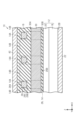
- FIG. 3 is a schematic cross-sectional view of the semiconductor device 10 taken along line F3-F3 in FIG.
- FIG. 3 shows a cross section of the first trench 24 in the XZ plane in the non-intersecting region 14B (see FIG. 2), which corresponds to a cross section of the first trench 24 along the short direction.
- Epitaxial layer 20 includes a drift region 36 formed on semiconductor substrate 18 corresponding to a drain region, a body region 38 formed on drift region 36, and a source region 40 formed on body region 38. .
- the drain region formed by the semiconductor substrate 18 may be an n-type region containing n-type impurities.
- the n-type impurity concentration of the semiconductor substrate 18 may be 1 ⁇ 10 18 cm ⁇ 3 or more and 1 ⁇ 10 20 cm ⁇ 3 or less.
- the semiconductor substrate 18 may have a thickness of 50 ⁇ m or more and 450 ⁇ m or less.
- the drift region 36 may be an n-type region containing n-type impurities at a lower concentration than the semiconductor substrate 18 (drain region).
- the n-type impurity concentration of the drift region 36 may be 1 ⁇ 10 15 cm ⁇ 3 or more and 1 ⁇ 10 18 cm ⁇ 3 or less.
- the drift region 36 may have a thickness of 1 ⁇ m or more and 25 ⁇ m or less.
- Body region 38 may be a p-type region containing p-type impurities.
- the p-type impurity concentration of the body region 38 may be 1 ⁇ 10 16 cm ⁇ 3 or more and 1 ⁇ 10 18 cm ⁇ 3 or less.
- Body region 38 may have a thickness of 0.2 ⁇ m or more and 1.0 ⁇ m or less.
- Source region 40 may be an n-type region containing a higher concentration of n-type impurities than drift region 36 .
- the n-type impurity concentration of the source region 40 may be 1 ⁇ 10 19 cm ⁇ 3 or more and 1 ⁇ 10 21 cm ⁇ 3 or less.
- the source region 40 may have a thickness of 0.1 ⁇ m or more and 1 ⁇ m or less.
- the n-type is also referred to as a first conductivity type, and the p-type is also referred to as a second conductivity type.
- the n-type impurity may be, for example, phosphorus (P) or arsenic (As).
- the p-type impurity may be, for example, boron (B), aluminum (Al), or the like.
- the first trench 24 has an opening in the upper surface 12A of the semiconductor layer 12, and has a side wall 24A and a bottom wall 24B.
- First trench 24 penetrates source region 40 and body region 38 of epitaxial layer 20 and reaches drift region 36 . Therefore, the bottom wall 24B of the first trench 24 is adjacent to the drift region 36.
- the first trench 24 may have a depth of 1 ⁇ m or more and 10 ⁇ m or less. Note that the depth of the first trench 24 may correspond to the distance from the top surface 12A of the semiconductor layer 12 to the bottom wall 24B of the first trench 24 in the Z-axis direction.
- the sidewall 24A of the first trench 24 may extend in the Z-axis direction (direction perpendicular to the upper surface 12A of the semiconductor layer 12) or may be inclined with respect to the Z-axis direction. In one example, the side wall 24A may be inclined with respect to the Z-axis direction so that the width of the first trench 24 becomes smaller toward the bottom wall 24B. Note that in that case, the width W1 of the first trench 24 shown in FIG. 2 may be the width of the first trench 24 at the position of the upper surface 12A of the semiconductor layer 12. Further, the bottom wall 24B of the first trench 24 does not necessarily have to be flat, and may be partially or entirely curved, for example.
- the gate electrode 28 is buried in the first trench 24 with the insulating layer 16 interposed therebetween.
- the gate electrode 28 is separated from the semiconductor layer 12 (epitaxial layer 20) by the insulating layer 16.
- Gate electrode 28 may be configured to have a gate voltage applied thereto. At least a portion of the gate electrode 28 may be arranged to face the body region 38 in the second direction with the insulating layer 16 in between.
- the gate electrode 28 may include a top surface 28A covered with the insulating layer 16 and a bottom surface 28B opposite to the top surface 28A.
- the insulating layer 16 is embedded between the bottom surface 28B of the gate electrode 28 and the bottom wall 24B of the first trench 24, and the field plate electrode 30 (see FIG. 1) are not placed.
- the upper surface 28A of the gate electrode 28 may be located below the upper surface 12A of the semiconductor layer 12 in the Z-axis direction. Further, the bottom surface 28B of the gate electrode 28 is located near the interface between the drift region 36 and the body region 38 in the Z-axis direction, and preferably may be located below the interface.
- the top surface 28A and bottom surface 28B of the gate electrode 28 may be flat or curved.
- the semiconductor device 10 may further include a source wiring 42 formed on the insulating layer 16.
- the source wiring 42 may be configured to be applied with a reference voltage (source voltage).
- the source wiring 42 is connected to the source contact plug 34.
- Epitaxial layer 20 may further include a contact region 44 adjacent body region 38 .
- Contact region 44 may be a p-type region containing p-type impurities.
- the p-type impurity concentration of the contact region 44 is higher than that of the body region 38, and may be 1 ⁇ 10 19 cm ⁇ 3 or more and 1 ⁇ 10 21 cm ⁇ 3 or less.
- Source contact plug 34 extends through insulating layer 16 and source region 40 so as to be in contact with contact region 44 .
- Contact region 44 may be adjacent to the bottom of source contact plug 34 .
- Contact region 44 is electrically connected to source wiring 42 via source contact plug 34 .
- the insulating layer 16 includes a gate insulating portion 46 that is interposed between the gate electrode 28 and the semiconductor layer 12 (epitaxial layer 20) and covers the side wall 24A of the first trench 24.
- the gate insulating portion 46 is a part of the insulating layer 16 between the side surface 28C of the gate electrode 28 and the side wall 24A of the first trench 24.
- Gate electrode 28 faces semiconductor layer 12 with gate insulating section 46 in between.
- a predetermined voltage gate voltage
- the semiconductor device 10 can control the flow of electrons in the Z-axis direction between the n-type source region 40 and the n-type drift region 36 via this channel.
- FIG. 4 is a schematic cross-sectional view of the semiconductor device 10 taken along line F4-F4 in FIG.
- FIG. 4 shows a cross section of the second trench 26 in the YZ plane in the non-intersecting region 14B (see FIG. 2), which corresponds to a cross section of the second trench 26 along the short direction.
- the second trench 26 has an opening in the upper surface 12A of the semiconductor layer 12, and has a side wall 26A and a bottom wall 26B. Second trench 26 penetrates source region 40 and body region 38 of epitaxial layer 20 and reaches drift region 36 . Therefore, the bottom wall 26B of the second trench 26 is adjacent to the drift region 36.
- the second trench 26 may have a depth of 1 ⁇ m or more and 10 ⁇ m or less. Note that the depth of the second trench 26 may correspond to the distance from the top surface 12A of the semiconductor layer 12 to the bottom wall 26B of the second trench 26 in the Z-axis direction.
- the sidewall 26A of the second trench 26 may extend in the Z-axis direction (direction perpendicular to the upper surface 12A of the semiconductor layer 12) or may be inclined with respect to the Z-axis direction. In one example, the side wall 26A may be inclined with respect to the Z-axis direction so that the width of the second trench 26 becomes smaller toward the bottom wall 26B. Note that in that case, the width W2 of the second trench 26 shown in FIG. 2 may be the width of the second trench 26 at the position of the upper surface 12A of the semiconductor layer 12. Further, the bottom wall 26B of the second trench 26 does not necessarily have to be flat, and may be partially or entirely curved, for example.
- the field plate electrode 30 is embedded in the second trench 26 with the insulating layer 16 interposed therebetween.
- Field plate electrode 30 is separated from semiconductor layer 12 (epitaxial layer 20) by insulating layer 16.
- the field plate electrode 30 may be configured to be applied with a reference voltage (source voltage). Therefore, the field plate electrode 30 may be electrically connected to the source wiring 42.
- Field plate electrode 30 is arranged below the interface between drift region 36 and body region 38 in the depth direction (Z-axis direction) of cell trench 14 .
- the field plate electrode 30 may include a top surface 30A covered with the insulating layer 16 and a bottom surface 30B opposite to the top surface 30A.
- the insulating layer 16 is embedded in the second trench 26 above the upper surface 30A of the field plate electrode 30, and the gate electrode 28 (see FIG. 1) is Not placed.
- the top surface 30A and bottom surface 30B of the field plate electrode 30 may be flat or curved.
- each field plate electrode 30 in the first direction is smaller than the dimension of each gate electrode 28 (see FIG. 3) in the second direction (X-axis direction in the illustrated example). good.
- FIG. 5 is a schematic cross-sectional view of the semiconductor device 10 taken along line F5-F5 in FIG. 2.
- FIG. 5 shows a cross section of the first trench 24 in the YZ plane, which corresponds to a cross section along the longitudinal direction of the first trench 24.
- intersecting regions 14A and non-intersecting regions 14B included in the first trench 24 are arranged alternately in the first direction in which the first trench 24 extends (in the illustrated example, the Y-axis direction).
- gate electrode 28 passes above field plate electrode 30.
- the field plate electrode 30 is not arranged below the gate electrode 28.
- FIG. 6 is a schematic cross-sectional view of the semiconductor device 10 taken along line F6-F6 in FIG.
- FIG. 6 shows a cross section of the second trench 26 in the XZ plane, which corresponds to a cross section along the longitudinal direction of the second trench 26.
- the intersecting regions 14A and non-intersecting regions 14B included in the second trench 26 are arranged alternately in the second direction in which the second trench 26 extends (in the illustrated example, the X-axis direction).
- the field plate electrode 30 passes below the gate electrode 28.
- the gate electrode 28 is not arranged above the field plate electrode 30.
- a field plate electrode 30 is arranged below the gate electrode 28 in the cell trench 14 in the intersection region 14A. At least a portion of the bottom surface 28B of the gate electrode 28 faces the top surface 30A of the field plate electrode 30 with the insulating layer 16 in between. Note that, as shown in FIG. 6, in the intersection region 14A, the side surface 28C of the gate electrode 28 does not face the side wall 24A of the first trench 24. Therefore, no channel is formed around the gate electrode 28 in the intersection region 14A. Therefore, as the ratio of the interval S2 between the second trenches 26 to the pitch P2 of the second trenches 26 is increased, a wider channel is formed, so that the on-resistance of the semiconductor device 10 can be reduced (see FIG. 2). .
- the non-intersecting region 14B only one of the gate electrode 28 and the field plate electrode 30 is arranged in the cell trench 14. More specifically, as shown in FIG. 5, in the non-intersecting region 14B included in the first trench 24, only the gate electrode 28 is disposed in the cell trench 14. Further, as shown in FIG. 6, in the non-intersecting region 14B included in the second trench 26, only the field plate electrode 30 is disposed in the cell trench 14. Therefore, in the non-intersecting region 14B, the gate electrode 28 and the field plate electrode 30 do not face each other in the depth direction (Z-axis direction) of the cell trench 14. As a result, the larger the ratio of the interval S1 of the first trenches 24 to the pitch P1 of the first trenches 24 is, the more the capacitance generated by the gate electrode 28 and the field plate electrode 30 can be reduced (see FIG. 2).
- the gate electrode 28 extends in the first direction, while the field plate electrode 30 extends in the second direction intersecting the first direction. Since the gate electrode 28 and the field plate electrode 30 do not extend in the same direction but intersect with each other, the capacitance caused by the gate electrode 28 and the field plate electrode 30 can be reduced.
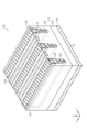
- FIG. 7 is a schematic cross-sectional perspective view of an exemplary semiconductor device 100 according to a comparative example.
- the same components as those of the semiconductor device 10 shown in FIGS. 1 to 6 are given the same reference numerals. Furthermore, detailed description of the same components as those of the semiconductor device 10 will be omitted.
- the semiconductor device 100 may be a MISFET having a trench gate structure.
- the semiconductor device 100 includes a drain electrode 22, a semiconductor layer 12 formed on the drain electrode 22, a plurality of cell trenches 102 formed in the semiconductor layer 12, and an insulating layer 16 formed on the semiconductor layer 12. include.
- FIG. 7 shows a cross-sectional view of the semiconductor device 100 at the position of the upper surface 12A of the semiconductor layer 12. It should be noted that, as shown in FIG. 8, the insulating layer 16 is formed not only within the cell trench 102 but also on the upper surface 12A of the semiconductor layer 12.
- the plurality of cell trenches 102 are arranged in a stripe pattern.
- Each of the plurality of cell trenches 102 extends in one direction (in the illustrated example, the Y-axis direction), has an opening in the upper surface 12A of the semiconductor layer 12, and has a depth in the Z-axis direction.
- the semiconductor device 100 includes a gate electrode 104 and a field plate electrode 106 buried in each cell trench 102 with an insulating layer 16 interposed therebetween. Gate electrode 104 and field plate electrode 106 extend in the direction in which cell trench 102 extends (ie, the Y-axis direction).
- the gate electrode 104 is located above the field plate electrode 106 (closer to the upper surface 12A of the semiconductor layer 12). Gate electrode 104 is separated from field plate electrode 106 by insulating layer 16 . Like the cell trench 102, the gate electrode 104 and the field plate electrode 106 extend in the Y-axis direction.
- the semiconductor device 100 further includes a plurality of source contact plugs 108.
- Each source contact plug 108 is arranged between two cell trenches 102. Like the cell trench 102, the source contact plug 108 extends in the Y-axis direction.
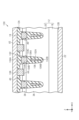
- FIG. 8 is a schematic cross-sectional view of the semiconductor device 100 shown in FIG. 7.
- FIG. 8 shows a cross section of the cell trench 102 in the XZ plane, which corresponds to a cross section along the short direction of the cell trench 102.
- Semiconductor device 100 further includes a source wiring 42 formed on insulating layer 16.
- Source wiring 42 is connected to source contact plug 108.
- the cell trench 102 has a side wall 102A and a bottom wall 102B. Cell trench 102 penetrates source region 40 and body region 38 of epitaxial layer 20 and reaches drift region 36 . Therefore, the bottom wall 102B of the cell trench 102 is adjacent to the drift region 36.
- the gate electrode 104 includes a top surface 104A covered with the insulating layer 16 and a bottom surface 104B opposite to the top surface 104A. Further, the side surface 104C of the gate electrode 104 faces the side wall 102A of the cell trench 102 with the gate insulating section 46 interposed therebetween.
- Field plate electrode 106 includes a top surface 106A covered by insulating layer 16, and a bottom surface 106B opposite top surface 106A. Field plate electrode 106 is arranged below gate electrode 104 within cell trench 102 . More specifically, the field plate electrode 106 is arranged between the bottom surface 104B of the gate electrode 104 and the bottom wall 102B of the cell trench 102. At least a portion of the bottom surface 104B of the gate electrode 104 faces the top surface 106A of the field plate electrode 106 with the insulating layer 16 in between.
- the gate electrode 104 and the field plate electrode 106 are surrounded by an insulating layer 16.
- Field plate electrode 106 has a smaller width than gate electrode 104. Due to the relatively small width of field plate electrode 106, the thickness of insulating layer 16 surrounding field plate electrode 106 is relatively large.
- the gate electrode 104 is configured so that a gate voltage is applied. Further, the field plate electrode 106 is configured to be applied with a reference voltage (source voltage). Therefore, the field plate electrode 106 can be electrically connected to the source wiring 42.
- a reference voltage source voltage
- the gate electrode 104 and the field plate electrode 106 extend in the same direction within the cell trench 102 while facing each other, the gate-source capacitance can become relatively large. If the gate-source capacitance is large, undesirable operations of the semiconductor device 100 such as self-turn-on may occur.
- the gate electrode 28 extends in the first direction in the cell trench 14 arranged in a mesh shape, while the field plate electrode 30 extends in the second direction intersecting the first direction. extending in the direction. Therefore, the capacitance caused by the gate electrode 28 and the field plate electrode 30 can be reduced.
- the cell trench 14 includes a plurality of intersection regions 14A where a plurality of first trenches 24 and a plurality of second trenches 26 intersect with each other, and a plurality of intersection regions 14A where a plurality of first trenches 24 and a plurality of second trenches 26 intersect with each other. It includes a plurality of non-intersecting regions 14B that do not intersect with each other.
- one of the plurality of gate electrodes 28 intersects with one of the plurality of field plate electrodes 30 in plan view.
- one of the plurality of gate electrodes 28 or one of the field plate electrodes 30 is arranged in the cell trench 14.
- each non-intersecting region 14B only one of the gate electrode 28 and the field plate electrode 30 is disposed in the cell trench 14, so that the capacitance caused by the gate electrode 28 and the field plate electrode 30 can be reduced. can.
- a field plate electrode 30 is arranged below the gate electrode 28 in the cell trench 14. Therefore, a depletion layer can be expanded in the semiconductor layer 12 near the intersection region 14A, and as a result, the gate-drain capacitance of the semiconductor device 10 can be reduced.
- the semiconductor device 10 of this embodiment has the following advantages. (1) In the cell trenches 14 arranged in a mesh shape, the gate electrode 28 extends in a first direction, while the field plate electrode 30 extends in a second direction intersecting the first direction. Since the gate electrode 28 and the field plate electrode 30 do not extend in the same direction but intersect with each other, the capacitance caused by the gate electrode 28 and the field plate electrode 30 can be reduced.
- the cell trench 14 includes a plurality of intersection regions 14A where a plurality of first trenches 24 and a plurality of second trenches 26 intersect with each other, and a plurality of intersection regions 14A where a plurality of first trenches 24 and a plurality of second trenches 26 intersect with each other. It includes a plurality of non-intersecting regions 14B.
- one of the plurality of gate electrodes 28 intersects with one of the plurality of field plate electrodes 30 in plan view.
- one of the plurality of gate electrodes 28 or one of the field plate electrodes 30 is arranged in the cell trench 14. Therefore, both the gate electrode 28 and the field plate electrode 30 can be arranged in the intersection region 14A, and only one of the gate electrode 28 and the field plate electrode 30 can be arranged in the non-intersection region 14B. Can be done.
- one of the plurality of field plate electrodes 30 is arranged below one of the plurality of gate electrodes 28 in the cell trench 14. Thereby, a depletion layer can be expanded in the semiconductor layer 12 near the intersection region 14A, and as a result, the gate-drain capacitance of the semiconductor device 10 can be reduced.
- the plurality of first trenches 24 are arranged parallel to each other at constant intervals S1, and the interval S1 at which the plurality of first trenches 24 are arranged is larger than the width W1 of each of the plurality of first trenches 24. It's okay. Thereby, the ratio of the interval S1 between the first trenches 24 to the pitch P1 of the first trenches 24 can be increased, so that the capacitance caused by the gate electrode 28 and the field plate electrode 30 can be further reduced.
- the plurality of second trenches 26 are arranged parallel to each other at constant intervals S2, and the interval S2 at which the plurality of second trenches 26 are arranged is larger than the width W2 of each of the plurality of second trenches 26. It's okay. As a result, the ratio of the interval S2 between the second trenches 26 to the pitch P2 of the second trenches 26 can be increased, so that a wider channel is formed, and as a result, the on-resistance of the semiconductor device 10 can be reduced. Can be done.
- the width W2 of each of the plurality of second trenches 26 may be larger than the width W1 of each of the plurality of first trenches 24. As the width W2 of the second trench 26 is increased, the insulation layer 16 surrounding the field plate electrode 30 can be made thicker, so that the breakdown voltage of the semiconductor device 10 can be improved.
- each field plate electrode 30 in the first direction may be smaller than the dimension of each gate electrode 28 in the second direction.
- FIG. 9 is a schematic plan view of an exemplary semiconductor device 200 for explaining a modification of the cell trench.
- the same components as those of the semiconductor device 10 shown in FIGS. 1 to 6 are given the same reference numerals. Furthermore, detailed description of the same components as those of the semiconductor device 10 will be omitted.
- the semiconductor device 200 includes a cell trench 202 formed in the semiconductor layer 12.
- the cell trench 202 includes a plurality of first trenches 24 extending in a first direction in a plan view, and a plurality of second trenches 26 extending in a second direction intersecting the first direction in a plan view.
- Cell trench 202 differs from exemplary cell trench 14 shown in FIGS. 1 and 2 in that the first direction in which first trench 24 extends does not coincide with the Y-axis direction.
- the angle between the first direction and the second direction is not 90 degrees. That is, the first direction may be inclined with respect to the direction orthogonal to the second direction.
- each of the plurality of first trenches 24 by tilting each of the plurality of first trenches 24 with respect to the Y-axis direction, they can be formed within a predetermined range of the semiconductor layer 12, compared to the example of FIG.
- the length of the first trench 24 can be increased. Since the gate electrode 28 is disposed in the first trench 24, the gate electrode 28 can be made longer by making each of the plurality of first trenches 24 inclined with respect to the Y-axis direction. As a result, the on-resistance of the semiconductor device 200 can be reduced.
- the first direction in which the first trenches 24 extend and the direction in which the second trenches 26 extend are The angle between the two directions is preferably within the range of 90 degrees ⁇ 10 degrees.
- the depth of the cell trench 14 is shown to be constant in both the crossing region 14A and the non-crossing region 14B.
- the depth of the cell trench 14 does not necessarily have to be constant.
- the depth of the cell trench 14 in the crossing region 14A may be greater than the depth of the cell trench 14 in the non-crossing region 14B.
- the depth of the cell trench 14 in the crossing region 14A may be smaller than the depth of the cell trench 14 in the non-crossing region 14B.
- the depth of the first trench 24 may be the same as or different from the depth of the second trench 26.
- the depth of the second trench 26 may be greater than the depth of the first trench 24.
- the depth of second trench 26 may be less than the depth of first trench 24.
- the source contact plug 34 extends in the Y-axis direction in plan view, but may be arranged so as to extend in the first direction parallel to the first trench 24.
- a structure in which the conductivity type of each region in the semiconductor layer 12 is reversed may be adopted. That is, the p-type region may be made into an n-type region, and the n-type region may be made into a p-type region.
- An additional wiring structure may be formed on the layer including the source wiring 42.
- the term “on” includes the meanings of “on” and “above” unless the context clearly indicates otherwise.
- the phrase “the first layer is formed on the second layer” refers to the fact that in some embodiments the first layer may be directly disposed on the second layer in contact with the second layer, but in other embodiments. It is contemplated that the first layer may be placed above the second layer without contacting the second layer. That is, the term “on” does not exclude structures in which other layers are formed between the first layer and the second layer.
- the Z-axis direction used in the present disclosure does not necessarily need to be a vertical direction, nor does it need to completely coincide with the vertical direction.
- the X-axis direction may be a vertical direction
- the Y-axis direction may be a vertical direction.
- a semiconductor layer (12) Cell trenches (14) formed in the semiconductor layer (12) and arranged in a mesh pattern include a plurality of first trenches (24) extending in a first direction in plan view; a plurality of second trenches (26) extending in a second direction intersecting the direction, the plurality of first trenches (24) and the plurality of second trenches (26) intersect with each other and communicate with each other.
- a semiconductor device comprising: a plurality of field plate electrodes (30) embedded in the plurality of second trenches (26) via the insulating layer (16) and extending in the second direction.
- the cell trench (14) includes a plurality of intersection regions (14A) where the plurality of first trenches (24) and the plurality of second trenches (26) intersect with each other, and the plurality of first trenches (24). and a plurality of non-intersecting regions (14B) in which the plurality of second trenches (26) do not intersect with each other, In each of the plurality of crossing regions (14A), one of the plurality of gate electrodes (28) intersects with one of the plurality of field plate electrodes (30), In each of the plurality of non-intersecting regions (14B), one of the plurality of gate electrodes (28) or one of the field plate electrodes (30) is located in the cell trench (14).
- the semiconductor device according to supplementary note 1, which is arranged.
- one of the plurality of field plate electrodes (30) is connected to one of the plurality of gate electrodes (28) in the cell trench (14).
- one of the plurality of field plate electrodes (30) is separated from one of the plurality of gate electrodes (28) by the insulating layer (16).
- the intersecting regions (14A) and the non-intersecting regions (14B) included in each of the plurality of first trenches (24) are arranged alternately in the first direction
- the intersecting regions (14A) and the non-intersecting regions (14B) included in each of the plurality of second trenches (26) are semiconductors according to appendix 2 or 3, wherein the intersecting regions (14A) and the non-intersecting regions (14B) are arranged alternately in the second direction.
- the semiconductor layer (12) includes a first conductivity type drift region (36), a second conductivity type body region (38) formed on the drift region (36), and a second conductivity type body region (38) formed on the body region (38).
- the source region (40) of the first conductivity type formed in At least a portion of each gate electrode (28) is arranged to face the body region (38) in the second direction with the insulating layer (16) interposed therebetween;
- Each field plate electrode (30) is arranged below the interface between the drift region (36) and the body region (38) in the depth direction of the cell trench (14).
- the semiconductor layer (12) includes a plurality of mesh regions (32) surrounded by the cell trenches (14) arranged in a mesh shape, The semiconductor device according to any one of appendices 1 to 6, wherein the plurality of source contact plugs (34) are respectively arranged in the plurality of mesh regions (32).
- Appendix 10 The semiconductor device according to any one of appendices 1 to 9, wherein the angle between the first direction and the second direction is within a range of 90 degrees ⁇ 10 degrees.
- the plurality of first trenches (24) are arranged parallel to each other at regular intervals (S1), Any one of Supplementary Notes 1 to 10, wherein the interval (S1) in which the plurality of first trenches (24) are arranged is larger than the width (W1) of each of the plurality of first trenches (24).
- the semiconductor device described in is described in .
- the width (W2) of each of the plurality of second trenches (26) is greater than the width (W1) of each of the plurality of first trenches (24), according to any one of Supplementary notes 1 to 12.
Landscapes
- Electrodes Of Semiconductors (AREA)
Priority Applications (1)
| Application Number | Priority Date | Filing Date | Title |
|---|---|---|---|
| JP2024545483A JPWO2024053267A1 (https=) | 2022-09-06 | 2023-07-21 |
Applications Claiming Priority (2)
| Application Number | Priority Date | Filing Date | Title |
|---|---|---|---|
| JP2022141444 | 2022-09-06 | ||
| JP2022-141444 | 2022-09-06 |
Publications (1)
| Publication Number | Publication Date |
|---|---|
| WO2024053267A1 true WO2024053267A1 (ja) | 2024-03-14 |
Family
ID=90192408
Family Applications (1)
| Application Number | Title | Priority Date | Filing Date |
|---|---|---|---|
| PCT/JP2023/026844 Ceased WO2024053267A1 (ja) | 2022-09-06 | 2023-07-21 | 半導体装置 |
Country Status (2)
| Country | Link |
|---|---|
| JP (1) | JPWO2024053267A1 (https=) |
| WO (1) | WO2024053267A1 (https=) |
Cited By (1)
| Publication number | Priority date | Publication date | Assignee | Title |
|---|---|---|---|---|
| US20240154007A1 (en) * | 2022-11-07 | 2024-05-09 | Rohm Co., Ltd. | Semiconductor device |
Citations (5)
| Publication number | Priority date | Publication date | Assignee | Title |
|---|---|---|---|---|
| JP2012059943A (ja) * | 2010-09-09 | 2012-03-22 | Toshiba Corp | 半導体装置 |
| US20130105886A1 (en) * | 2011-11-01 | 2013-05-02 | Alpha And Omega Semiconductor Incorporated | Two-dimensional shielded gate transistor device and method of manufacture |
| US9252263B1 (en) * | 2014-07-31 | 2016-02-02 | Infineon Technologies Austria Ag | Multiple semiconductor device trenches per cell pitch |
| JP2021192400A (ja) * | 2020-06-05 | 2021-12-16 | ローム株式会社 | 半導体装置 |
| JP2022045628A (ja) * | 2020-09-09 | 2022-03-22 | 株式会社東芝 | 半導体装置 |
-
2023
- 2023-07-21 JP JP2024545483A patent/JPWO2024053267A1/ja active Pending
- 2023-07-21 WO PCT/JP2023/026844 patent/WO2024053267A1/ja not_active Ceased
Patent Citations (5)
| Publication number | Priority date | Publication date | Assignee | Title |
|---|---|---|---|---|
| JP2012059943A (ja) * | 2010-09-09 | 2012-03-22 | Toshiba Corp | 半導体装置 |
| US20130105886A1 (en) * | 2011-11-01 | 2013-05-02 | Alpha And Omega Semiconductor Incorporated | Two-dimensional shielded gate transistor device and method of manufacture |
| US9252263B1 (en) * | 2014-07-31 | 2016-02-02 | Infineon Technologies Austria Ag | Multiple semiconductor device trenches per cell pitch |
| JP2021192400A (ja) * | 2020-06-05 | 2021-12-16 | ローム株式会社 | 半導体装置 |
| JP2022045628A (ja) * | 2020-09-09 | 2022-03-22 | 株式会社東芝 | 半導体装置 |
Cited By (1)
| Publication number | Priority date | Publication date | Assignee | Title |
|---|---|---|---|---|
| US20240154007A1 (en) * | 2022-11-07 | 2024-05-09 | Rohm Co., Ltd. | Semiconductor device |
Also Published As
| Publication number | Publication date |
|---|---|
| JPWO2024053267A1 (https=) | 2024-03-14 |
Similar Documents
| Publication | Publication Date | Title |
|---|---|---|
| JP7207463B2 (ja) | 半導体装置 | |
| US11088276B2 (en) | Silicon carbide semiconductor device | |
| US20240421199A1 (en) | Semiconductor device | |
| JP7818572B2 (ja) | 半導体装置 | |
| CN100485970C (zh) | 带有结型场效应晶体管的碳化硅半导体器件及其制造方法 | |
| US20240387648A1 (en) | Semiconductor device | |
| WO2022264694A1 (ja) | 半導体装置 | |
| WO2024053267A1 (ja) | 半導体装置 | |
| US20240363710A1 (en) | Semiconductor device | |
| US20250015176A1 (en) | Semiconductor device | |
| US20060284217A1 (en) | Silicon carbide semiconductor device | |
| US20240154007A1 (en) | Semiconductor device | |
| JP2022146898A (ja) | 半導体装置および半導体装置の製造方法 | |
| US20240055474A1 (en) | Semiconductor device | |
| JP2023069720A (ja) | 半導体装置 | |
| WO2023135896A1 (ja) | 半導体装置 | |
| JP2025187244A (ja) | 半導体装置 | |
| US20230145576A1 (en) | Semiconductor device | |
| JP2025147937A (ja) | 半導体装置 | |
| JP2026001948A (ja) | 半導体装置 | |
| JP2025175906A (ja) | 半導体デバイス | |
| JP2023060584A (ja) | 半導体装置 | |
| JP2025004503A (ja) | 半導体装置 | |
| WO2023188755A1 (ja) | 半導体装置 | |
| JP2026004061A (ja) | 半導体装置及び半導体装置の製造方法 |
Legal Events
| Date | Code | Title | Description |
|---|---|---|---|
| 121 | Ep: the epo has been informed by wipo that ep was designated in this application |
Ref document number: 23862811 Country of ref document: EP Kind code of ref document: A1 |
|
| WWE | Wipo information: entry into national phase |
Ref document number: 2024545483 Country of ref document: JP |
|
| NENP | Non-entry into the national phase |
Ref country code: DE |
|
| 122 | Ep: pct application non-entry in european phase |
Ref document number: 23862811 Country of ref document: EP Kind code of ref document: A1 |