WO2024053267A1 - Semiconductor device - Google Patents
Semiconductor device Download PDFInfo
- Publication number
- WO2024053267A1 WO2024053267A1 PCT/JP2023/026844 JP2023026844W WO2024053267A1 WO 2024053267 A1 WO2024053267 A1 WO 2024053267A1 JP 2023026844 W JP2023026844 W JP 2023026844W WO 2024053267 A1 WO2024053267 A1 WO 2024053267A1
- Authority
- WO
- WIPO (PCT)
- Prior art keywords
- trenches
- semiconductor device
- field plate
- trench
- semiconductor
- Prior art date
Links
- 239000004065 semiconductor Substances 0.000 title claims abstract description 161
- 210000000746 body region Anatomy 0.000 claims description 24
- 238000000034 method Methods 0.000 claims description 2
- 239000012535 impurity Substances 0.000 description 12
- 239000000758 substrate Substances 0.000 description 10
- PXHVJJICTQNCMI-UHFFFAOYSA-N Nickel Chemical compound [Ni] PXHVJJICTQNCMI-UHFFFAOYSA-N 0.000 description 3
- 230000000052 comparative effect Effects 0.000 description 3
- 230000004048 modification Effects 0.000 description 3
- 238000012986 modification Methods 0.000 description 3
- 229910052581 Si3N4 Inorganic materials 0.000 description 2
- 229910052782 aluminium Inorganic materials 0.000 description 2
- 239000010949 copper Substances 0.000 description 2
- 239000010931 gold Substances 0.000 description 2
- HQVNEWCFYHHQES-UHFFFAOYSA-N silicon nitride Chemical compound N12[Si]34N5[Si]62N3[Si]51N64 HQVNEWCFYHHQES-UHFFFAOYSA-N 0.000 description 2
- 239000010936 titanium Substances 0.000 description 2
- 229910000838 Al alloy Inorganic materials 0.000 description 1
- ZOXJGFHDIHLPTG-UHFFFAOYSA-N Boron Chemical compound [B] ZOXJGFHDIHLPTG-UHFFFAOYSA-N 0.000 description 1
- RYGMFSIKBFXOCR-UHFFFAOYSA-N Copper Chemical compound [Cu] RYGMFSIKBFXOCR-UHFFFAOYSA-N 0.000 description 1
- 229910000881 Cu alloy Inorganic materials 0.000 description 1
- OAICVXFJPJFONN-UHFFFAOYSA-N Phosphorus Chemical compound [P] OAICVXFJPJFONN-UHFFFAOYSA-N 0.000 description 1
- 229910004298 SiO 2 Inorganic materials 0.000 description 1
- VYPSYNLAJGMNEJ-UHFFFAOYSA-N Silicium dioxide Chemical compound O=[Si]=O VYPSYNLAJGMNEJ-UHFFFAOYSA-N 0.000 description 1
- XUIMIQQOPSSXEZ-UHFFFAOYSA-N Silicon Chemical compound [Si] XUIMIQQOPSSXEZ-UHFFFAOYSA-N 0.000 description 1
- BQCADISMDOOEFD-UHFFFAOYSA-N Silver Chemical compound [Ag] BQCADISMDOOEFD-UHFFFAOYSA-N 0.000 description 1
- RTAQQCXQSZGOHL-UHFFFAOYSA-N Titanium Chemical compound [Ti] RTAQQCXQSZGOHL-UHFFFAOYSA-N 0.000 description 1
- XAGFODPZIPBFFR-UHFFFAOYSA-N aluminium Chemical compound [Al] XAGFODPZIPBFFR-UHFFFAOYSA-N 0.000 description 1
- 229910052785 arsenic Inorganic materials 0.000 description 1
- RQNWIZPPADIBDY-UHFFFAOYSA-N arsenic atom Chemical compound [As] RQNWIZPPADIBDY-UHFFFAOYSA-N 0.000 description 1
- 229910052796 boron Inorganic materials 0.000 description 1
- 230000015556 catabolic process Effects 0.000 description 1
- 229910052802 copper Inorganic materials 0.000 description 1
- 230000005684 electric field Effects 0.000 description 1
- 230000005669 field effect Effects 0.000 description 1
- PCHJSUWPFVWCPO-UHFFFAOYSA-N gold Chemical compound [Au] PCHJSUWPFVWCPO-UHFFFAOYSA-N 0.000 description 1
- 229910052737 gold Inorganic materials 0.000 description 1
- 230000012447 hatching Effects 0.000 description 1
- 238000009413 insulation Methods 0.000 description 1
- 239000007769 metal material Substances 0.000 description 1
- 229910052759 nickel Inorganic materials 0.000 description 1
- 229910052698 phosphorus Inorganic materials 0.000 description 1
- 239000011574 phosphorus Substances 0.000 description 1
- 229910021420 polycrystalline silicon Inorganic materials 0.000 description 1
- 229920005591 polysilicon Polymers 0.000 description 1
- 229910052710 silicon Inorganic materials 0.000 description 1
- 239000010703 silicon Substances 0.000 description 1
- 229910052814 silicon oxide Inorganic materials 0.000 description 1
- 229910052709 silver Inorganic materials 0.000 description 1
- 239000004332 silver Substances 0.000 description 1
- 229910052719 titanium Inorganic materials 0.000 description 1
Images


Classifications
-
- H—ELECTRICITY
- H01—ELECTRIC ELEMENTS
- H01L—SEMICONDUCTOR DEVICES NOT COVERED BY CLASS H10
- H01L29/00—Semiconductor devices adapted for rectifying, amplifying, oscillating or switching, or capacitors or resistors with at least one potential-jump barrier or surface barrier, e.g. PN junction depletion layer or carrier concentration layer; Details of semiconductor bodies or of electrodes thereof ; Multistep manufacturing processes therefor
- H01L29/02—Semiconductor bodies ; Multistep manufacturing processes therefor
- H01L29/06—Semiconductor bodies ; Multistep manufacturing processes therefor characterised by their shape; characterised by the shapes, relative sizes, or dispositions of the semiconductor regions ; characterised by the concentration or distribution of impurities within semiconductor regions
-
- H—ELECTRICITY
- H01—ELECTRIC ELEMENTS
- H01L—SEMICONDUCTOR DEVICES NOT COVERED BY CLASS H10
- H01L29/00—Semiconductor devices adapted for rectifying, amplifying, oscillating or switching, or capacitors or resistors with at least one potential-jump barrier or surface barrier, e.g. PN junction depletion layer or carrier concentration layer; Details of semiconductor bodies or of electrodes thereof ; Multistep manufacturing processes therefor
- H01L29/66—Types of semiconductor device ; Multistep manufacturing processes therefor
- H01L29/68—Types of semiconductor device ; Multistep manufacturing processes therefor controllable by only the electric current supplied, or only the electric potential applied, to an electrode which does not carry the current to be rectified, amplified or switched
- H01L29/76—Unipolar devices, e.g. field effect transistors
- H01L29/772—Field effect transistors
- H01L29/78—Field effect transistors with field effect produced by an insulated gate
Definitions
- the present disclosure relates to a semiconductor device.
- Patent Document 1 discloses a semiconductor device having a plurality of trench gate structures formed in a stripe shape. Each trench gate structure includes a gate trench and two electrodes buried separately in the depth direction of the gate trench.
- the gate electrode and the field plate electrode When the gate electrode and the field plate electrode are buried separately in the gate trench, the gate electrode and the field plate electrode extend into the gate trench while facing each other. If the capacitance created by the gate electrode and the field plate electrode is relatively large, undesirable behavior of the semiconductor device, such as self-turn-on, can be caused.
- a semiconductor device includes a semiconductor layer, a plurality of first trenches formed in the semiconductor layer and arranged in a mesh shape, and extending in a first direction in a plan view; a plurality of second trenches extending in a second direction intersecting the first direction when viewed, the plurality of first trenches and the plurality of second trenches intersecting and communicating with each other; an insulating layer formed on the semiconductor layer; a plurality of gate electrodes each embedded in the plurality of first trenches via the insulating layer and extending in the first direction; and a plurality of second trenches.
- a plurality of field plate electrodes are respectively embedded in the trenches via the insulating layer and extend in the second direction.
- the capacitance caused by the gate electrode and the field plate electrode can be reduced.
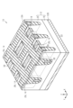
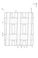
- FIG. 1 is a schematic cross-sectional perspective view of an exemplary semiconductor device according to one embodiment.
- FIG. 2 is a schematic plan view of the semiconductor device shown in FIG. 1.
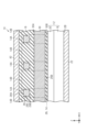
- FIG. 3 is a schematic cross-sectional view of the semiconductor device taken along line F3-F3 in FIG.
- FIG. 4 is a schematic cross-sectional view of the semiconductor device taken along line F4-F4 in FIG.
- FIG. 5 is a schematic cross-sectional view of the semiconductor device taken along line F5-F5 in FIG.
- FIG. 6 is a schematic cross-sectional view of the semiconductor device taken along line F6-F6 in FIG.
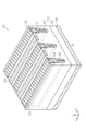
- FIG. 7 is a schematic cross-sectional perspective view of an exemplary semiconductor device according to a comparative example.
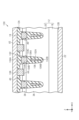
- FIG. 8 is a schematic cross-sectional view of the semiconductor device shown in FIG. 7.
- FIG. 9 is a schematic plan view of a semiconductor device according to a modification example.
- FIG. 1 is a schematic cross-sectional perspective view of an exemplary semiconductor device 10 according to one embodiment.
- FIG. 2 is a schematic plan view of the semiconductor device 10.
- the semiconductor device 10 may be, for example, a MISFET (Metal-Insulator-Semiconductor Field Effect Transistor) having a trench gate structure.
- the semiconductor device 10 includes a semiconductor layer 12 , a cell trench 14 formed in the semiconductor layer 12 , and an insulating layer 16 formed on the semiconductor layer 12 .
- the semiconductor layer 12 may include a semiconductor substrate 18 and an epitaxial layer 20, and the cell trench 14 may be formed in the epitaxial layer 20.
- the semiconductor substrate 18 may be a silicon (Si) substrate.
- the epitaxial layer 20 may be a Si epitaxial layer.
- the top surface 12A of the semiconductor layer 12 may be included in the epitaxial layer 20, while the bottom surface 12B of the semiconductor layer 12 may be included in the semiconductor substrate 18.
- Insulating layer 16 may include at least one of a silicon oxide (SiO 2 ) layer and a silicon nitride (SiN) layer.
- a cross-sectional view and a plan view of the semiconductor device 10 at the position of the upper surface 12A of the semiconductor layer 12 are shown, respectively, for ease of understanding (line F1-F1 in FIG. 3). reference). It should be noted that, as shown in FIG. 3, the insulating layer 16 is formed not only within the cell trench 14 but also on the upper surface 12A of the semiconductor layer 12.
- the semiconductor device 10 may further include a drain electrode 22 formed on the bottom surface 12B of the semiconductor layer 12.
- Drain electrode 22 may be formed from at least one of titanium (Ti), nickel (Ni), gold (Au), silver (Ag), copper (Cu), Al, Cu alloy, and Al alloy. .
- the cell trench 14 includes a plurality of first trenches 24 extending in a first direction in plan view and a plurality of second trenches extending in a second direction intersecting the first direction in plan view. 26.
- the Z-axis direction of the mutually orthogonal XYZ axes shown in FIGS. 1 and 2 is a direction that is orthogonal to the surface of the semiconductor layer 12.
- the term "planar view” used in this specification refers to viewing the semiconductor device 10 from above along the Z-axis direction, unless explicitly stated otherwise.
- the first direction is the longitudinal direction of the first trench 24, and the second direction is the longitudinal direction of the second trench 26. In the example shown in FIGS.
- the first direction may be the Y-axis direction
- the second direction may be the X-axis direction. Therefore, in the illustrated example, the angle between the first direction and the second direction is 90 degrees. Note that, as will be described later with reference to FIG. 9, the first direction and the second direction do not necessarily have to correspond to the Y-axis direction and the X-axis direction, respectively.
- the cell trench 14 has an opening in the upper surface 12A of the semiconductor layer 12 and has a depth in the Z-axis direction.
- the plurality of first trenches 24 and the plurality of second trenches 26 intersect and communicate with each other. Thereby, the cell trenches 14 are arranged in a mesh shape.
- the cell trench 14 includes a plurality of intersection regions 14A where a plurality of first trenches 24 and a plurality of second trenches 26 intersect with each other, and a plurality of first trenches 24 and a plurality of second trenches 26. and a plurality of non-intersecting regions 14B that do not intersect with each other.
- the plurality of first trenches 24 may be arranged in stripes.
- each of the plurality of first trenches 24 has a width W1.
- the width W1 of the first trench 24 corresponds to the dimension of the first trench 24 in the lateral direction (that is, the direction perpendicular to the first direction) in plan view.
- the plurality of first trenches 24 can be arranged parallel to each other at a constant interval S1.
- the plurality of second trenches 26 may be arranged in a stripe pattern.
- each of the plurality of second trenches 26 has a width W2.
- the width W2 of the second trench 26 corresponds to the dimension of the second trench 26 in the lateral direction (that is, the direction orthogonal to the second direction) in plan view.
- the plurality of second trenches 26 can be arranged parallel to each other at constant intervals S2.
- the interval S1 between the plurality of first trenches 24 may be larger than the width W1 of each of the plurality of first trenches 24.
- the interval S2 between the plurality of second trenches 26 may be larger than the width W2 of each of the plurality of second trenches 26.
- the width W2 of each of the plurality of second trenches 26 may be larger than the width W1 of each of the plurality of first trenches 24.
- the interval S2 between the plurality of second trenches 26 may be larger than the interval S1 between the plurality of first trenches 24. Therefore, the pitch P2 (the sum of the width W2 and the interval S2) of the second trenches 26 may be larger than the pitch P1 (the sum of the width W1 and the interval S1) of the first trenches 24.
- the pitch P1 of the first trenches 24 may be approximately the same as the spacing S2 of the second trenches 26.
- the semiconductor device 10 further includes a plurality of gate electrodes 28 embedded in the plurality of first trenches 24 with an insulating layer 16 interposed therebetween.
- the plurality of gate electrodes 28 extend in the first direction.
- the semiconductor device 10 further includes a plurality of field plate electrodes 30 embedded in the plurality of second trenches 26 with the insulating layer 16 interposed therebetween.
- the plurality of field plate electrodes 30 extend in the second direction.
- Gate electrode 28 and field plate electrode 30 may be formed from conductive polysilicon, in one example. In other examples, gate electrode 28 and field plate electrode 30 may be formed from any other metallic material.
- the plurality of gate electrodes 28 are located above the plurality of field plate electrodes 30 (closer to the upper surface 12A of the semiconductor layer 12) in the cell trench 14.
- the plurality of gate electrodes 28 are separated from the plurality of field plate electrodes 30 by the insulating layer 16.
- Each of the plurality of gate electrodes 28 crosses the plurality of field plate electrodes 30 by passing over the plurality of field plate electrodes 30.
- Each of the plurality of field plate electrodes 30 intersects with the plurality of gate electrodes 28 by passing under the plurality of gate electrodes 28 .
- one of the plurality of gate electrodes 28 intersects with one of the plurality of field plate electrodes 30 in each of the plurality of intersection regions 14A. Further, in each of the plurality of non-intersecting regions 14B, one of the plurality of gate electrodes 28 or one of the field plate electrodes 30 is arranged in the cell trench 14.
- the semiconductor layer 12 can include a plurality of mesh regions 32 (see FIG. 2) surrounded by cell trenches 14 arranged in a mesh shape. Each of the plurality of mesh regions 32 may have a rectangular shape in plan view.
- the semiconductor device 10 may further include a plurality of source contact plugs 34 arranged in the plurality of mesh regions 32, respectively. Details of the source contact plug 34 will be described later with reference to FIG. 3.
- FIG. 3 is a schematic cross-sectional view of the semiconductor device 10 taken along line F3-F3 in FIG.
- FIG. 3 shows a cross section of the first trench 24 in the XZ plane in the non-intersecting region 14B (see FIG. 2), which corresponds to a cross section of the first trench 24 along the short direction.
- Epitaxial layer 20 includes a drift region 36 formed on semiconductor substrate 18 corresponding to a drain region, a body region 38 formed on drift region 36, and a source region 40 formed on body region 38. .
- the drain region formed by the semiconductor substrate 18 may be an n-type region containing n-type impurities.
- the n-type impurity concentration of the semiconductor substrate 18 may be 1 ⁇ 10 18 cm ⁇ 3 or more and 1 ⁇ 10 20 cm ⁇ 3 or less.
- the semiconductor substrate 18 may have a thickness of 50 ⁇ m or more and 450 ⁇ m or less.
- the drift region 36 may be an n-type region containing n-type impurities at a lower concentration than the semiconductor substrate 18 (drain region).
- the n-type impurity concentration of the drift region 36 may be 1 ⁇ 10 15 cm ⁇ 3 or more and 1 ⁇ 10 18 cm ⁇ 3 or less.
- the drift region 36 may have a thickness of 1 ⁇ m or more and 25 ⁇ m or less.
- Body region 38 may be a p-type region containing p-type impurities.
- the p-type impurity concentration of the body region 38 may be 1 ⁇ 10 16 cm ⁇ 3 or more and 1 ⁇ 10 18 cm ⁇ 3 or less.
- Body region 38 may have a thickness of 0.2 ⁇ m or more and 1.0 ⁇ m or less.
- Source region 40 may be an n-type region containing a higher concentration of n-type impurities than drift region 36 .
- the n-type impurity concentration of the source region 40 may be 1 ⁇ 10 19 cm ⁇ 3 or more and 1 ⁇ 10 21 cm ⁇ 3 or less.
- the source region 40 may have a thickness of 0.1 ⁇ m or more and 1 ⁇ m or less.
- the n-type is also referred to as a first conductivity type, and the p-type is also referred to as a second conductivity type.
- the n-type impurity may be, for example, phosphorus (P) or arsenic (As).
- the p-type impurity may be, for example, boron (B), aluminum (Al), or the like.
- the first trench 24 has an opening in the upper surface 12A of the semiconductor layer 12, and has a side wall 24A and a bottom wall 24B.
- First trench 24 penetrates source region 40 and body region 38 of epitaxial layer 20 and reaches drift region 36 . Therefore, the bottom wall 24B of the first trench 24 is adjacent to the drift region 36.
- the first trench 24 may have a depth of 1 ⁇ m or more and 10 ⁇ m or less. Note that the depth of the first trench 24 may correspond to the distance from the top surface 12A of the semiconductor layer 12 to the bottom wall 24B of the first trench 24 in the Z-axis direction.
- the sidewall 24A of the first trench 24 may extend in the Z-axis direction (direction perpendicular to the upper surface 12A of the semiconductor layer 12) or may be inclined with respect to the Z-axis direction. In one example, the side wall 24A may be inclined with respect to the Z-axis direction so that the width of the first trench 24 becomes smaller toward the bottom wall 24B. Note that in that case, the width W1 of the first trench 24 shown in FIG. 2 may be the width of the first trench 24 at the position of the upper surface 12A of the semiconductor layer 12. Further, the bottom wall 24B of the first trench 24 does not necessarily have to be flat, and may be partially or entirely curved, for example.
- the gate electrode 28 is buried in the first trench 24 with the insulating layer 16 interposed therebetween.
- the gate electrode 28 is separated from the semiconductor layer 12 (epitaxial layer 20) by the insulating layer 16.
- Gate electrode 28 may be configured to have a gate voltage applied thereto. At least a portion of the gate electrode 28 may be arranged to face the body region 38 in the second direction with the insulating layer 16 in between.
- the gate electrode 28 may include a top surface 28A covered with the insulating layer 16 and a bottom surface 28B opposite to the top surface 28A.
- the insulating layer 16 is embedded between the bottom surface 28B of the gate electrode 28 and the bottom wall 24B of the first trench 24, and the field plate electrode 30 (see FIG. 1) are not placed.
- the upper surface 28A of the gate electrode 28 may be located below the upper surface 12A of the semiconductor layer 12 in the Z-axis direction. Further, the bottom surface 28B of the gate electrode 28 is located near the interface between the drift region 36 and the body region 38 in the Z-axis direction, and preferably may be located below the interface.
- the top surface 28A and bottom surface 28B of the gate electrode 28 may be flat or curved.
- the semiconductor device 10 may further include a source wiring 42 formed on the insulating layer 16.
- the source wiring 42 may be configured to be applied with a reference voltage (source voltage).
- the source wiring 42 is connected to the source contact plug 34.
- Epitaxial layer 20 may further include a contact region 44 adjacent body region 38 .
- Contact region 44 may be a p-type region containing p-type impurities.
- the p-type impurity concentration of the contact region 44 is higher than that of the body region 38, and may be 1 ⁇ 10 19 cm ⁇ 3 or more and 1 ⁇ 10 21 cm ⁇ 3 or less.
- Source contact plug 34 extends through insulating layer 16 and source region 40 so as to be in contact with contact region 44 .
- Contact region 44 may be adjacent to the bottom of source contact plug 34 .
- Contact region 44 is electrically connected to source wiring 42 via source contact plug 34 .
- the insulating layer 16 includes a gate insulating portion 46 that is interposed between the gate electrode 28 and the semiconductor layer 12 (epitaxial layer 20) and covers the side wall 24A of the first trench 24.
- the gate insulating portion 46 is a part of the insulating layer 16 between the side surface 28C of the gate electrode 28 and the side wall 24A of the first trench 24.
- Gate electrode 28 faces semiconductor layer 12 with gate insulating section 46 in between.
- a predetermined voltage gate voltage
- the semiconductor device 10 can control the flow of electrons in the Z-axis direction between the n-type source region 40 and the n-type drift region 36 via this channel.
- FIG. 4 is a schematic cross-sectional view of the semiconductor device 10 taken along line F4-F4 in FIG.
- FIG. 4 shows a cross section of the second trench 26 in the YZ plane in the non-intersecting region 14B (see FIG. 2), which corresponds to a cross section of the second trench 26 along the short direction.
- the second trench 26 has an opening in the upper surface 12A of the semiconductor layer 12, and has a side wall 26A and a bottom wall 26B. Second trench 26 penetrates source region 40 and body region 38 of epitaxial layer 20 and reaches drift region 36 . Therefore, the bottom wall 26B of the second trench 26 is adjacent to the drift region 36.
- the second trench 26 may have a depth of 1 ⁇ m or more and 10 ⁇ m or less. Note that the depth of the second trench 26 may correspond to the distance from the top surface 12A of the semiconductor layer 12 to the bottom wall 26B of the second trench 26 in the Z-axis direction.
- the sidewall 26A of the second trench 26 may extend in the Z-axis direction (direction perpendicular to the upper surface 12A of the semiconductor layer 12) or may be inclined with respect to the Z-axis direction. In one example, the side wall 26A may be inclined with respect to the Z-axis direction so that the width of the second trench 26 becomes smaller toward the bottom wall 26B. Note that in that case, the width W2 of the second trench 26 shown in FIG. 2 may be the width of the second trench 26 at the position of the upper surface 12A of the semiconductor layer 12. Further, the bottom wall 26B of the second trench 26 does not necessarily have to be flat, and may be partially or entirely curved, for example.
- the field plate electrode 30 is embedded in the second trench 26 with the insulating layer 16 interposed therebetween.
- Field plate electrode 30 is separated from semiconductor layer 12 (epitaxial layer 20) by insulating layer 16.
- the field plate electrode 30 may be configured to be applied with a reference voltage (source voltage). Therefore, the field plate electrode 30 may be electrically connected to the source wiring 42.
- Field plate electrode 30 is arranged below the interface between drift region 36 and body region 38 in the depth direction (Z-axis direction) of cell trench 14 .
- the field plate electrode 30 may include a top surface 30A covered with the insulating layer 16 and a bottom surface 30B opposite to the top surface 30A.
- the insulating layer 16 is embedded in the second trench 26 above the upper surface 30A of the field plate electrode 30, and the gate electrode 28 (see FIG. 1) is Not placed.
- the top surface 30A and bottom surface 30B of the field plate electrode 30 may be flat or curved.
- each field plate electrode 30 in the first direction is smaller than the dimension of each gate electrode 28 (see FIG. 3) in the second direction (X-axis direction in the illustrated example). good.
- FIG. 5 is a schematic cross-sectional view of the semiconductor device 10 taken along line F5-F5 in FIG. 2.
- FIG. 5 shows a cross section of the first trench 24 in the YZ plane, which corresponds to a cross section along the longitudinal direction of the first trench 24.
- intersecting regions 14A and non-intersecting regions 14B included in the first trench 24 are arranged alternately in the first direction in which the first trench 24 extends (in the illustrated example, the Y-axis direction).
- gate electrode 28 passes above field plate electrode 30.
- the field plate electrode 30 is not arranged below the gate electrode 28.
- FIG. 6 is a schematic cross-sectional view of the semiconductor device 10 taken along line F6-F6 in FIG.
- FIG. 6 shows a cross section of the second trench 26 in the XZ plane, which corresponds to a cross section along the longitudinal direction of the second trench 26.
- the intersecting regions 14A and non-intersecting regions 14B included in the second trench 26 are arranged alternately in the second direction in which the second trench 26 extends (in the illustrated example, the X-axis direction).
- the field plate electrode 30 passes below the gate electrode 28.
- the gate electrode 28 is not arranged above the field plate electrode 30.
- a field plate electrode 30 is arranged below the gate electrode 28 in the cell trench 14 in the intersection region 14A. At least a portion of the bottom surface 28B of the gate electrode 28 faces the top surface 30A of the field plate electrode 30 with the insulating layer 16 in between. Note that, as shown in FIG. 6, in the intersection region 14A, the side surface 28C of the gate electrode 28 does not face the side wall 24A of the first trench 24. Therefore, no channel is formed around the gate electrode 28 in the intersection region 14A. Therefore, as the ratio of the interval S2 between the second trenches 26 to the pitch P2 of the second trenches 26 is increased, a wider channel is formed, so that the on-resistance of the semiconductor device 10 can be reduced (see FIG. 2). .
- the non-intersecting region 14B only one of the gate electrode 28 and the field plate electrode 30 is arranged in the cell trench 14. More specifically, as shown in FIG. 5, in the non-intersecting region 14B included in the first trench 24, only the gate electrode 28 is disposed in the cell trench 14. Further, as shown in FIG. 6, in the non-intersecting region 14B included in the second trench 26, only the field plate electrode 30 is disposed in the cell trench 14. Therefore, in the non-intersecting region 14B, the gate electrode 28 and the field plate electrode 30 do not face each other in the depth direction (Z-axis direction) of the cell trench 14. As a result, the larger the ratio of the interval S1 of the first trenches 24 to the pitch P1 of the first trenches 24 is, the more the capacitance generated by the gate electrode 28 and the field plate electrode 30 can be reduced (see FIG. 2).
- the gate electrode 28 extends in the first direction, while the field plate electrode 30 extends in the second direction intersecting the first direction. Since the gate electrode 28 and the field plate electrode 30 do not extend in the same direction but intersect with each other, the capacitance caused by the gate electrode 28 and the field plate electrode 30 can be reduced.
- FIG. 7 is a schematic cross-sectional perspective view of an exemplary semiconductor device 100 according to a comparative example.
- the same components as those of the semiconductor device 10 shown in FIGS. 1 to 6 are given the same reference numerals. Furthermore, detailed description of the same components as those of the semiconductor device 10 will be omitted.
- the semiconductor device 100 may be a MISFET having a trench gate structure.
- the semiconductor device 100 includes a drain electrode 22, a semiconductor layer 12 formed on the drain electrode 22, a plurality of cell trenches 102 formed in the semiconductor layer 12, and an insulating layer 16 formed on the semiconductor layer 12. include.
- FIG. 7 shows a cross-sectional view of the semiconductor device 100 at the position of the upper surface 12A of the semiconductor layer 12. It should be noted that, as shown in FIG. 8, the insulating layer 16 is formed not only within the cell trench 102 but also on the upper surface 12A of the semiconductor layer 12.
- the plurality of cell trenches 102 are arranged in a stripe pattern.
- Each of the plurality of cell trenches 102 extends in one direction (in the illustrated example, the Y-axis direction), has an opening in the upper surface 12A of the semiconductor layer 12, and has a depth in the Z-axis direction.
- the semiconductor device 100 includes a gate electrode 104 and a field plate electrode 106 buried in each cell trench 102 with an insulating layer 16 interposed therebetween. Gate electrode 104 and field plate electrode 106 extend in the direction in which cell trench 102 extends (ie, the Y-axis direction).
- the gate electrode 104 is located above the field plate electrode 106 (closer to the upper surface 12A of the semiconductor layer 12). Gate electrode 104 is separated from field plate electrode 106 by insulating layer 16 . Like the cell trench 102, the gate electrode 104 and the field plate electrode 106 extend in the Y-axis direction.
- the semiconductor device 100 further includes a plurality of source contact plugs 108.
- Each source contact plug 108 is arranged between two cell trenches 102. Like the cell trench 102, the source contact plug 108 extends in the Y-axis direction.
- FIG. 8 is a schematic cross-sectional view of the semiconductor device 100 shown in FIG. 7.
- FIG. 8 shows a cross section of the cell trench 102 in the XZ plane, which corresponds to a cross section along the short direction of the cell trench 102.
- Semiconductor device 100 further includes a source wiring 42 formed on insulating layer 16.
- Source wiring 42 is connected to source contact plug 108.
- the cell trench 102 has a side wall 102A and a bottom wall 102B. Cell trench 102 penetrates source region 40 and body region 38 of epitaxial layer 20 and reaches drift region 36 . Therefore, the bottom wall 102B of the cell trench 102 is adjacent to the drift region 36.
- the gate electrode 104 includes a top surface 104A covered with the insulating layer 16 and a bottom surface 104B opposite to the top surface 104A. Further, the side surface 104C of the gate electrode 104 faces the side wall 102A of the cell trench 102 with the gate insulating section 46 interposed therebetween.
- Field plate electrode 106 includes a top surface 106A covered by insulating layer 16, and a bottom surface 106B opposite top surface 106A. Field plate electrode 106 is arranged below gate electrode 104 within cell trench 102 . More specifically, the field plate electrode 106 is arranged between the bottom surface 104B of the gate electrode 104 and the bottom wall 102B of the cell trench 102. At least a portion of the bottom surface 104B of the gate electrode 104 faces the top surface 106A of the field plate electrode 106 with the insulating layer 16 in between.
- the gate electrode 104 and the field plate electrode 106 are surrounded by an insulating layer 16.
- Field plate electrode 106 has a smaller width than gate electrode 104. Due to the relatively small width of field plate electrode 106, the thickness of insulating layer 16 surrounding field plate electrode 106 is relatively large.
- the gate electrode 104 is configured so that a gate voltage is applied. Further, the field plate electrode 106 is configured to be applied with a reference voltage (source voltage). Therefore, the field plate electrode 106 can be electrically connected to the source wiring 42.
- a reference voltage source voltage
- the gate electrode 104 and the field plate electrode 106 extend in the same direction within the cell trench 102 while facing each other, the gate-source capacitance can become relatively large. If the gate-source capacitance is large, undesirable operations of the semiconductor device 100 such as self-turn-on may occur.
- the gate electrode 28 extends in the first direction in the cell trench 14 arranged in a mesh shape, while the field plate electrode 30 extends in the second direction intersecting the first direction. extending in the direction. Therefore, the capacitance caused by the gate electrode 28 and the field plate electrode 30 can be reduced.
- the cell trench 14 includes a plurality of intersection regions 14A where a plurality of first trenches 24 and a plurality of second trenches 26 intersect with each other, and a plurality of intersection regions 14A where a plurality of first trenches 24 and a plurality of second trenches 26 intersect with each other. It includes a plurality of non-intersecting regions 14B that do not intersect with each other.
- one of the plurality of gate electrodes 28 intersects with one of the plurality of field plate electrodes 30 in plan view.
- one of the plurality of gate electrodes 28 or one of the field plate electrodes 30 is arranged in the cell trench 14.
- each non-intersecting region 14B only one of the gate electrode 28 and the field plate electrode 30 is disposed in the cell trench 14, so that the capacitance caused by the gate electrode 28 and the field plate electrode 30 can be reduced. can.
- a field plate electrode 30 is arranged below the gate electrode 28 in the cell trench 14. Therefore, a depletion layer can be expanded in the semiconductor layer 12 near the intersection region 14A, and as a result, the gate-drain capacitance of the semiconductor device 10 can be reduced.
- the semiconductor device 10 of this embodiment has the following advantages. (1) In the cell trenches 14 arranged in a mesh shape, the gate electrode 28 extends in a first direction, while the field plate electrode 30 extends in a second direction intersecting the first direction. Since the gate electrode 28 and the field plate electrode 30 do not extend in the same direction but intersect with each other, the capacitance caused by the gate electrode 28 and the field plate electrode 30 can be reduced.
- the cell trench 14 includes a plurality of intersection regions 14A where a plurality of first trenches 24 and a plurality of second trenches 26 intersect with each other, and a plurality of intersection regions 14A where a plurality of first trenches 24 and a plurality of second trenches 26 intersect with each other. It includes a plurality of non-intersecting regions 14B.
- one of the plurality of gate electrodes 28 intersects with one of the plurality of field plate electrodes 30 in plan view.
- one of the plurality of gate electrodes 28 or one of the field plate electrodes 30 is arranged in the cell trench 14. Therefore, both the gate electrode 28 and the field plate electrode 30 can be arranged in the intersection region 14A, and only one of the gate electrode 28 and the field plate electrode 30 can be arranged in the non-intersection region 14B. Can be done.
- one of the plurality of field plate electrodes 30 is arranged below one of the plurality of gate electrodes 28 in the cell trench 14. Thereby, a depletion layer can be expanded in the semiconductor layer 12 near the intersection region 14A, and as a result, the gate-drain capacitance of the semiconductor device 10 can be reduced.
- the plurality of first trenches 24 are arranged parallel to each other at constant intervals S1, and the interval S1 at which the plurality of first trenches 24 are arranged is larger than the width W1 of each of the plurality of first trenches 24. It's okay. Thereby, the ratio of the interval S1 between the first trenches 24 to the pitch P1 of the first trenches 24 can be increased, so that the capacitance caused by the gate electrode 28 and the field plate electrode 30 can be further reduced.
- the plurality of second trenches 26 are arranged parallel to each other at constant intervals S2, and the interval S2 at which the plurality of second trenches 26 are arranged is larger than the width W2 of each of the plurality of second trenches 26. It's okay. As a result, the ratio of the interval S2 between the second trenches 26 to the pitch P2 of the second trenches 26 can be increased, so that a wider channel is formed, and as a result, the on-resistance of the semiconductor device 10 can be reduced. Can be done.
- the width W2 of each of the plurality of second trenches 26 may be larger than the width W1 of each of the plurality of first trenches 24. As the width W2 of the second trench 26 is increased, the insulation layer 16 surrounding the field plate electrode 30 can be made thicker, so that the breakdown voltage of the semiconductor device 10 can be improved.
- each field plate electrode 30 in the first direction may be smaller than the dimension of each gate electrode 28 in the second direction.
- FIG. 9 is a schematic plan view of an exemplary semiconductor device 200 for explaining a modification of the cell trench.
- the same components as those of the semiconductor device 10 shown in FIGS. 1 to 6 are given the same reference numerals. Furthermore, detailed description of the same components as those of the semiconductor device 10 will be omitted.
- the semiconductor device 200 includes a cell trench 202 formed in the semiconductor layer 12.
- the cell trench 202 includes a plurality of first trenches 24 extending in a first direction in a plan view, and a plurality of second trenches 26 extending in a second direction intersecting the first direction in a plan view.
- Cell trench 202 differs from exemplary cell trench 14 shown in FIGS. 1 and 2 in that the first direction in which first trench 24 extends does not coincide with the Y-axis direction.
- the angle between the first direction and the second direction is not 90 degrees. That is, the first direction may be inclined with respect to the direction orthogonal to the second direction.
- each of the plurality of first trenches 24 by tilting each of the plurality of first trenches 24 with respect to the Y-axis direction, they can be formed within a predetermined range of the semiconductor layer 12, compared to the example of FIG.
- the length of the first trench 24 can be increased. Since the gate electrode 28 is disposed in the first trench 24, the gate electrode 28 can be made longer by making each of the plurality of first trenches 24 inclined with respect to the Y-axis direction. As a result, the on-resistance of the semiconductor device 200 can be reduced.
- the first direction in which the first trenches 24 extend and the direction in which the second trenches 26 extend are The angle between the two directions is preferably within the range of 90 degrees ⁇ 10 degrees.
- the depth of the cell trench 14 is shown to be constant in both the crossing region 14A and the non-crossing region 14B.
- the depth of the cell trench 14 does not necessarily have to be constant.
- the depth of the cell trench 14 in the crossing region 14A may be greater than the depth of the cell trench 14 in the non-crossing region 14B.
- the depth of the cell trench 14 in the crossing region 14A may be smaller than the depth of the cell trench 14 in the non-crossing region 14B.
- the depth of the first trench 24 may be the same as or different from the depth of the second trench 26.
- the depth of the second trench 26 may be greater than the depth of the first trench 24.
- the depth of second trench 26 may be less than the depth of first trench 24.
- the source contact plug 34 extends in the Y-axis direction in plan view, but may be arranged so as to extend in the first direction parallel to the first trench 24.
- a structure in which the conductivity type of each region in the semiconductor layer 12 is reversed may be adopted. That is, the p-type region may be made into an n-type region, and the n-type region may be made into a p-type region.
- An additional wiring structure may be formed on the layer including the source wiring 42.
- the term “on” includes the meanings of “on” and “above” unless the context clearly indicates otherwise.
- the phrase “the first layer is formed on the second layer” refers to the fact that in some embodiments the first layer may be directly disposed on the second layer in contact with the second layer, but in other embodiments. It is contemplated that the first layer may be placed above the second layer without contacting the second layer. That is, the term “on” does not exclude structures in which other layers are formed between the first layer and the second layer.
- the Z-axis direction used in the present disclosure does not necessarily need to be a vertical direction, nor does it need to completely coincide with the vertical direction.
- the X-axis direction may be a vertical direction
- the Y-axis direction may be a vertical direction.
- a semiconductor layer (12) Cell trenches (14) formed in the semiconductor layer (12) and arranged in a mesh pattern include a plurality of first trenches (24) extending in a first direction in plan view; a plurality of second trenches (26) extending in a second direction intersecting the direction, the plurality of first trenches (24) and the plurality of second trenches (26) intersect with each other and communicate with each other.
- a semiconductor device comprising: a plurality of field plate electrodes (30) embedded in the plurality of second trenches (26) via the insulating layer (16) and extending in the second direction.
- the cell trench (14) includes a plurality of intersection regions (14A) where the plurality of first trenches (24) and the plurality of second trenches (26) intersect with each other, and the plurality of first trenches (24). and a plurality of non-intersecting regions (14B) in which the plurality of second trenches (26) do not intersect with each other, In each of the plurality of crossing regions (14A), one of the plurality of gate electrodes (28) intersects with one of the plurality of field plate electrodes (30), In each of the plurality of non-intersecting regions (14B), one of the plurality of gate electrodes (28) or one of the field plate electrodes (30) is located in the cell trench (14).
- the semiconductor device according to supplementary note 1, which is arranged.
- one of the plurality of field plate electrodes (30) is connected to one of the plurality of gate electrodes (28) in the cell trench (14).
- one of the plurality of field plate electrodes (30) is separated from one of the plurality of gate electrodes (28) by the insulating layer (16).
- the intersecting regions (14A) and the non-intersecting regions (14B) included in each of the plurality of first trenches (24) are arranged alternately in the first direction
- the intersecting regions (14A) and the non-intersecting regions (14B) included in each of the plurality of second trenches (26) are semiconductors according to appendix 2 or 3, wherein the intersecting regions (14A) and the non-intersecting regions (14B) are arranged alternately in the second direction.
- the semiconductor layer (12) includes a first conductivity type drift region (36), a second conductivity type body region (38) formed on the drift region (36), and a second conductivity type body region (38) formed on the body region (38).
- the source region (40) of the first conductivity type formed in At least a portion of each gate electrode (28) is arranged to face the body region (38) in the second direction with the insulating layer (16) interposed therebetween;
- Each field plate electrode (30) is arranged below the interface between the drift region (36) and the body region (38) in the depth direction of the cell trench (14).
- the semiconductor layer (12) includes a plurality of mesh regions (32) surrounded by the cell trenches (14) arranged in a mesh shape, The semiconductor device according to any one of appendices 1 to 6, wherein the plurality of source contact plugs (34) are respectively arranged in the plurality of mesh regions (32).
- Appendix 10 The semiconductor device according to any one of appendices 1 to 9, wherein the angle between the first direction and the second direction is within a range of 90 degrees ⁇ 10 degrees.
- the plurality of first trenches (24) are arranged parallel to each other at regular intervals (S1), Any one of Supplementary Notes 1 to 10, wherein the interval (S1) in which the plurality of first trenches (24) are arranged is larger than the width (W1) of each of the plurality of first trenches (24).
- the semiconductor device described in is described in .
- the width (W2) of each of the plurality of second trenches (26) is greater than the width (W1) of each of the plurality of first trenches (24), according to any one of Supplementary notes 1 to 12.
Abstract
This semiconductor device (10) is provided with: a semiconductor layer (12); a cell trench (14) which is formed in the shape of a mesh in the semiconductor layer (12), while comprising a plurality of first trenches (24) that extend in a first direction when viewed in plan and a plurality of second trenches (26) that extend in a second direction that intersects with the first direction when viewed in plan so that the plurality of first trenches (24) and the plurality of second trenches (26) intersect with and in communication with each other; an insulating layer (16) which is formed on the semiconductor layer (12); a plurality of gate electrodes (28) which are respectively buried in the plurality of first trenches (24) by the intermediary of the insulating layer (16), while extending in the first direction; and a plurality of field plate electrodes (30) which are respectively buried in the plurality of second trenches (26) by the intermediary of the insulating layer (16), while extending in the second direction.
Description
本開示は、半導体装置に関する。
The present disclosure relates to a semiconductor device.
特許文献1は、ストライプ状に形成された複数のトレンチゲート構造を有する半導体装置を開示している。各トレンチゲート構造は、ゲートトレンチと、ゲートトレンチの深さ方向に分離して埋め込まれた2つの電極を含んでいる。
Patent Document 1 discloses a semiconductor device having a plurality of trench gate structures formed in a stripe shape. Each trench gate structure includes a gate trench and two electrodes buried separately in the depth direction of the gate trench.
ゲートトレンチ内にゲート電極およびフィールドプレート電極が分離して埋め込まれる場合、ゲート電極とフィールドプレート電極とは、互いに対向しつつ、ゲートトレンチ内に延在している。ゲート電極とフィールドプレート電極とにより生じる容量が比較的大きい場合、セルフターンオンなどの半導体装置の望ましくない動作が引き起こされ得る。
When the gate electrode and the field plate electrode are buried separately in the gate trench, the gate electrode and the field plate electrode extend into the gate trench while facing each other. If the capacitance created by the gate electrode and the field plate electrode is relatively large, undesirable behavior of the semiconductor device, such as self-turn-on, can be caused.
本開示の一態様による半導体装置は、半導体層と、前記半導体層に形成されるとともにメッシュ状に配置されたセルトレンチであって、平面視で第1方向に延びる複数の第1トレンチと、平面視で前記第1方向と交差する第2方向に延びる複数の第2トレンチとを含み、前記複数の第1トレンチと前記複数の第2トレンチとは互いに交差し、かつ連通している、セルトレンチと、前記半導体層上に形成された絶縁層と、前記複数の第1トレンチ内に前記絶縁層を介してそれぞれ埋め込まれるとともに、前記第1方向に延びる複数のゲート電極と、前記複数の第2トレンチ内に前記絶縁層を介してそれぞれ埋め込まれるとともに、前記第2方向に延びる複数のフィールドプレート電極とを備えている。
A semiconductor device according to one aspect of the present disclosure includes a semiconductor layer, a plurality of first trenches formed in the semiconductor layer and arranged in a mesh shape, and extending in a first direction in a plan view; a plurality of second trenches extending in a second direction intersecting the first direction when viewed, the plurality of first trenches and the plurality of second trenches intersecting and communicating with each other; an insulating layer formed on the semiconductor layer; a plurality of gate electrodes each embedded in the plurality of first trenches via the insulating layer and extending in the first direction; and a plurality of second trenches. A plurality of field plate electrodes are respectively embedded in the trenches via the insulating layer and extend in the second direction.
本開示の半導体装置によれば、ゲート電極とフィールドプレート電極とにより生じる容量を低減することができる。
According to the semiconductor device of the present disclosure, the capacitance caused by the gate electrode and the field plate electrode can be reduced.
以下、添付図面を参照して本開示の半導体装置のいくつかの実施形態を説明する。なお、説明を簡単かつ明確にするために、図面に示される構成要素は必ずしも一定の縮尺で描かれていない。また、理解を容易にするために、断面図では、ハッチング線が省略されている場合がある。添付の図面は、本開示の実施形態を例示するに過ぎず、本開示を制限するものとみなされるべきではない。
Hereinafter, some embodiments of the semiconductor device of the present disclosure will be described with reference to the accompanying drawings. It should be noted that, for simplicity and clarity of explanation, the components shown in the drawings are not necessarily drawn to scale. Further, in order to facilitate understanding, hatching lines may be omitted in the cross-sectional views. The accompanying drawings are merely illustrative of embodiments of the disclosure and should not be considered as limiting the disclosure.
以下の詳細な記載は、本開示の例示的な実施形態を具体化する装置、システム、および方法を含む。この詳細な記載は本来説明のためのものに過ぎず、本開示の実施形態またはこのような実施形態の適用および使用を限定することを意図しない。
The following detailed description includes devices, systems, and methods that embody example embodiments of the present disclosure. This detailed description is illustrative in nature and is not intended to limit the embodiments of the disclosure or the application and uses of such embodiments.
図1は、一実施形態に係る例示的な半導体装置10の概略断面斜視図である。図2は、半導体装置10の概略平面図である。半導体装置10は、例えばトレンチゲート構造を有するMISFET(Metal-Insulator-Semiconductor Field Effect Transistor)であってよい。半導体装置10は、半導体層12と、半導体層12に形成されたセルトレンチ14と、半導体層12上に形成された絶縁層16とを含む。図1に示すように、半導体層12は、半導体基板18と、エピタキシャル層20とを含んでいてよく、セルトレンチ14は、エピタキシャル層20に形成されていてよい。本実施形態において、半導体基板18は、シリコン(Si)基板であってよい。また、エピタキシャル層20は、Siエピタキシャル層であってよい。半導体層12の上面12Aは、エピタキシャル層20に含まれ、一方、半導体層12の底面12Bは、半導体基板18に含まれていてよい。絶縁層16は、酸化シリコン(SiO2)層および窒化シリコン(SiN)層のうちの少なくとも1つを含んでいてよい。
FIG. 1 is a schematic cross-sectional perspective view of an exemplary semiconductor device 10 according to one embodiment. FIG. 2 is a schematic plan view of the semiconductor device 10. The semiconductor device 10 may be, for example, a MISFET (Metal-Insulator-Semiconductor Field Effect Transistor) having a trench gate structure. The semiconductor device 10 includes a semiconductor layer 12 , a cell trench 14 formed in the semiconductor layer 12 , and an insulating layer 16 formed on the semiconductor layer 12 . As shown in FIG. 1, the semiconductor layer 12 may include a semiconductor substrate 18 and an epitaxial layer 20, and the cell trench 14 may be formed in the epitaxial layer 20. In this embodiment, the semiconductor substrate 18 may be a silicon (Si) substrate. Further, the epitaxial layer 20 may be a Si epitaxial layer. The top surface 12A of the semiconductor layer 12 may be included in the epitaxial layer 20, while the bottom surface 12B of the semiconductor layer 12 may be included in the semiconductor substrate 18. Insulating layer 16 may include at least one of a silicon oxide (SiO 2 ) layer and a silicon nitride (SiN) layer.
なお、理解を容易にするために、図1および図2においては、半導体層12の上面12Aの位置における半導体装置10の断面図および平面図がそれぞれ示されている(図3のF1-F1線参照)。図3に示すように、絶縁層16は、セルトレンチ14内だけでなく、半導体層12の上面12A上にも形成されている点に留意されたい。
1 and 2, a cross-sectional view and a plan view of the semiconductor device 10 at the position of the upper surface 12A of the semiconductor layer 12 are shown, respectively, for ease of understanding (line F1-F1 in FIG. 3). reference). It should be noted that, as shown in FIG. 3, the insulating layer 16 is formed not only within the cell trench 14 but also on the upper surface 12A of the semiconductor layer 12.
半導体装置10は、半導体層12の底面12Bに形成されたドレイン電極22をさらに含んでいてよい。ドレイン電極22は、チタン(Ti)、ニッケル(Ni)、金(Au)、銀(Ag)、銅(Cu)、Al、Cu合金、およびAl合金のうちの少なくとも1つから形成されていてよい。
The semiconductor device 10 may further include a drain electrode 22 formed on the bottom surface 12B of the semiconductor layer 12. Drain electrode 22 may be formed from at least one of titanium (Ti), nickel (Ni), gold (Au), silver (Ag), copper (Cu), Al, Cu alloy, and Al alloy. .
(セルトレンチの詳細)
図1および図2に示すように、セルトレンチ14は、平面視で第1方向に延びる複数の第1トレンチ24と、平面視で第1方向と交差する第2方向に延びる複数の第2トレンチ26とを含む。なお、図1および図2に示される互いに直交するXYZ軸のZ軸方向は、半導体層12の面と直交する方向である。本明細書において使用される「平面視」という用語は、明示的に別段の記載がない限り、Z軸方向に沿って上方から半導体装置10を視ることをいう。第1方向は、第1トレンチ24の長手方向であり、第2方向は、第2トレンチ26の長手方向である。図1および図2に示す例では、第1方向はY軸方向であり、第2方向はX軸方向であってよい。したがって、図示の例では、第1方向と第2方向とのなす角度は90度である。なお、図9を参照して後述するように、第1方向および第2方向は、必ずしもY軸方向およびX軸方向にそれぞれ一致している必要はない。セルトレンチ14は、半導体層12の上面12Aに開口を有するとともに、Z軸方向に深さを有している。複数の第1トレンチ24と複数の第2トレンチ26とは互いに交差し、かつ連通している。これにより、セルトレンチ14は、メッシュ状に配置されている。 (Details of cell trench)
As shown in FIGS. 1 and 2, the cell trench 14 includes a plurality of first trenches 24 extending in a first direction in plan view and a plurality of second trenches extending in a second direction intersecting the first direction in plan view. 26. Note that the Z-axis direction of the mutually orthogonal XYZ axes shown in FIGS. 1 and 2 is a direction that is orthogonal to the surface of thesemiconductor layer 12. The term "planar view" used in this specification refers to viewing the semiconductor device 10 from above along the Z-axis direction, unless explicitly stated otherwise. The first direction is the longitudinal direction of the first trench 24, and the second direction is the longitudinal direction of the second trench 26. In the example shown in FIGS. 1 and 2, the first direction may be the Y-axis direction, and the second direction may be the X-axis direction. Therefore, in the illustrated example, the angle between the first direction and the second direction is 90 degrees. Note that, as will be described later with reference to FIG. 9, the first direction and the second direction do not necessarily have to correspond to the Y-axis direction and the X-axis direction, respectively. The cell trench 14 has an opening in the upper surface 12A of the semiconductor layer 12 and has a depth in the Z-axis direction. The plurality of first trenches 24 and the plurality of second trenches 26 intersect and communicate with each other. Thereby, the cell trenches 14 are arranged in a mesh shape.
図1および図2に示すように、セルトレンチ14は、平面視で第1方向に延びる複数の第1トレンチ24と、平面視で第1方向と交差する第2方向に延びる複数の第2トレンチ26とを含む。なお、図1および図2に示される互いに直交するXYZ軸のZ軸方向は、半導体層12の面と直交する方向である。本明細書において使用される「平面視」という用語は、明示的に別段の記載がない限り、Z軸方向に沿って上方から半導体装置10を視ることをいう。第1方向は、第1トレンチ24の長手方向であり、第2方向は、第2トレンチ26の長手方向である。図1および図2に示す例では、第1方向はY軸方向であり、第2方向はX軸方向であってよい。したがって、図示の例では、第1方向と第2方向とのなす角度は90度である。なお、図9を参照して後述するように、第1方向および第2方向は、必ずしもY軸方向およびX軸方向にそれぞれ一致している必要はない。セルトレンチ14は、半導体層12の上面12Aに開口を有するとともに、Z軸方向に深さを有している。複数の第1トレンチ24と複数の第2トレンチ26とは互いに交差し、かつ連通している。これにより、セルトレンチ14は、メッシュ状に配置されている。 (Details of cell trench)
As shown in FIGS. 1 and 2, the cell trench 14 includes a plurality of first trenches 24 extending in a first direction in plan view and a plurality of second trenches extending in a second direction intersecting the first direction in plan view. 26. Note that the Z-axis direction of the mutually orthogonal XYZ axes shown in FIGS. 1 and 2 is a direction that is orthogonal to the surface of the
図2に示すように、セルトレンチ14は、複数の第1トレンチ24と複数の第2トレンチ26とが互いに交差する複数の交差領域14Aと、複数の第1トレンチ24と複数の第2トレンチ26とが互いに交差していない複数の非交差領域14Bとを含んでいる。複数の第1トレンチ24は、ストライプ状に配置されていてよい。一例では、複数の第1トレンチ24の各々は、幅W1を有している。第1トレンチ24の幅W1は、平面視における第1トレンチ24の短手方向(すなわち、第1方向と直交する方向)の寸法に相当する。複数の第1トレンチ24は、一定の間隔S1で互いに平行に配置することができる。同様に、複数の第2トレンチ26は、ストライプ状に配置されていてよい。一例では、複数の第2トレンチ26の各々は、幅W2を有している。第2トレンチ26の幅W2は、平面視における第2トレンチ26の短手方向(すなわち、第2方向と直交する方向)の寸法に相当する。複数の第2トレンチ26は、一定の間隔S2で互いに平行に配置することができる。
As shown in FIG. 2, the cell trench 14 includes a plurality of intersection regions 14A where a plurality of first trenches 24 and a plurality of second trenches 26 intersect with each other, and a plurality of first trenches 24 and a plurality of second trenches 26. and a plurality of non-intersecting regions 14B that do not intersect with each other. The plurality of first trenches 24 may be arranged in stripes. In one example, each of the plurality of first trenches 24 has a width W1. The width W1 of the first trench 24 corresponds to the dimension of the first trench 24 in the lateral direction (that is, the direction perpendicular to the first direction) in plan view. The plurality of first trenches 24 can be arranged parallel to each other at a constant interval S1. Similarly, the plurality of second trenches 26 may be arranged in a stripe pattern. In one example, each of the plurality of second trenches 26 has a width W2. The width W2 of the second trench 26 corresponds to the dimension of the second trench 26 in the lateral direction (that is, the direction orthogonal to the second direction) in plan view. The plurality of second trenches 26 can be arranged parallel to each other at constant intervals S2.
一例では、複数の第1トレンチ24が配置される間隔S1は、複数の第1トレンチ24の各々の幅W1よりも大きくてよい。また、一例では、複数の第2トレンチ26が配置される間隔S2は、複数の第2トレンチ26の各々の幅W2よりも大きくてよい。
In one example, the interval S1 between the plurality of first trenches 24 may be larger than the width W1 of each of the plurality of first trenches 24. Further, in one example, the interval S2 between the plurality of second trenches 26 may be larger than the width W2 of each of the plurality of second trenches 26.
一例では、複数の第2トレンチ26の各々の幅W2は、複数の第1トレンチ24の各々の幅W1よりも大きくてよい。また、一例では、複数の第2トレンチ26が配置される間隔S2は、複数の第1トレンチ24が配置される間隔S1よりも大きくてよい。したがって、第2トレンチ26のピッチP2(幅W2と間隔S2との合計)は、第1トレンチ24のピッチP1(幅W1と間隔S1との合計)よりも大きくてよい。一例では、第1トレンチ24のピッチP1は、第2トレンチ26の間隔S2と同程度であってよい。
In one example, the width W2 of each of the plurality of second trenches 26 may be larger than the width W1 of each of the plurality of first trenches 24. Further, in one example, the interval S2 between the plurality of second trenches 26 may be larger than the interval S1 between the plurality of first trenches 24. Therefore, the pitch P2 (the sum of the width W2 and the interval S2) of the second trenches 26 may be larger than the pitch P1 (the sum of the width W1 and the interval S1) of the first trenches 24. In one example, the pitch P1 of the first trenches 24 may be approximately the same as the spacing S2 of the second trenches 26.
図1および図2に示すように、半導体装置10は、複数の第1トレンチ24内に絶縁層16を介してそれぞれ埋め込まれた複数のゲート電極28をさらに含む。複数のゲート電極28は、第1方向に延びている。また、半導体装置10は、複数の第2トレンチ26内に絶縁層16を介してそれぞれ埋め込まれた複数のフィールドプレート電極30をさらに含む。複数のフィールドプレート電極30は、第2方向に延びている。ゲート電極28およびフィールドプレート電極30は、一例では、導電性のポリシリコンから形成されていてよい。別の例では、ゲート電極28およびフィールドプレート電極30は、他の任意の金属材料から形成されていてもよい。
As shown in FIGS. 1 and 2, the semiconductor device 10 further includes a plurality of gate electrodes 28 embedded in the plurality of first trenches 24 with an insulating layer 16 interposed therebetween. The plurality of gate electrodes 28 extend in the first direction. Further, the semiconductor device 10 further includes a plurality of field plate electrodes 30 embedded in the plurality of second trenches 26 with the insulating layer 16 interposed therebetween. The plurality of field plate electrodes 30 extend in the second direction. Gate electrode 28 and field plate electrode 30 may be formed from conductive polysilicon, in one example. In other examples, gate electrode 28 and field plate electrode 30 may be formed from any other metallic material.
複数のゲート電極28は、セルトレンチ14内において、複数のフィールドプレート電極30よりも上方(半導体層12の上面12A寄り)に位置している。複数のゲート電極28は、絶縁層16によって複数のフィールドプレート電極30から離隔されている。複数のゲート電極28の各々は、複数のフィールドプレート電極30の上方を通ることにより、複数のフィールドプレート電極30と交差している。複数のフィールドプレート電極30の各々は、複数のゲート電極28の下方を通ることにより、複数のゲート電極28と交差している。
The plurality of gate electrodes 28 are located above the plurality of field plate electrodes 30 (closer to the upper surface 12A of the semiconductor layer 12) in the cell trench 14. The plurality of gate electrodes 28 are separated from the plurality of field plate electrodes 30 by the insulating layer 16. Each of the plurality of gate electrodes 28 crosses the plurality of field plate electrodes 30 by passing over the plurality of field plate electrodes 30. Each of the plurality of field plate electrodes 30 intersects with the plurality of gate electrodes 28 by passing under the plurality of gate electrodes 28 .
図2に示すように、複数の交差領域14Aの各々において、複数のゲート電極28のうちの1つが、複数のフィールドプレート電極30のうちの1つと交差している。また、複数の非交差領域14Bの各々において、セルトレンチ14内には、複数のゲート電極28のうちの1つ、またはフィールドプレート電極30のうちの1つが配置されている。
As shown in FIG. 2, one of the plurality of gate electrodes 28 intersects with one of the plurality of field plate electrodes 30 in each of the plurality of intersection regions 14A. Further, in each of the plurality of non-intersecting regions 14B, one of the plurality of gate electrodes 28 or one of the field plate electrodes 30 is arranged in the cell trench 14.
半導体層12は、メッシュ状に配置されたセルトレンチ14によって囲まれた複数のメッシュ領域32(図2参照)を含むことができる。複数のメッシュ領域32の各々は、平面視で矩形状であってよい。半導体装置10は、複数のメッシュ領域32にそれぞれ配置された複数のソースコンタクトプラグ34をさらに含んでいてよい。ソースコンタクトプラグ34の詳細は、図3を参照して後述する。
The semiconductor layer 12 can include a plurality of mesh regions 32 (see FIG. 2) surrounded by cell trenches 14 arranged in a mesh shape. Each of the plurality of mesh regions 32 may have a rectangular shape in plan view. The semiconductor device 10 may further include a plurality of source contact plugs 34 arranged in the plurality of mesh regions 32, respectively. Details of the source contact plug 34 will be described later with reference to FIG. 3.
(半導体装置の断面構造)
図3は、図2のF3-F3線に沿った半導体装置10の概略断面図である。図3では、非交差領域14B(図2参照)における第1トレンチ24のXZ平面の断面が示されており、これは、第1トレンチ24の短手方向に沿った断面に相当する。 (Cross-sectional structure of semiconductor device)
FIG. 3 is a schematic cross-sectional view of thesemiconductor device 10 taken along line F3-F3 in FIG. FIG. 3 shows a cross section of the first trench 24 in the XZ plane in the non-intersecting region 14B (see FIG. 2), which corresponds to a cross section of the first trench 24 along the short direction.
図3は、図2のF3-F3線に沿った半導体装置10の概略断面図である。図3では、非交差領域14B(図2参照)における第1トレンチ24のXZ平面の断面が示されており、これは、第1トレンチ24の短手方向に沿った断面に相当する。 (Cross-sectional structure of semiconductor device)
FIG. 3 is a schematic cross-sectional view of the
エピタキシャル層20は、ドレイン領域に相当する半導体基板18上に形成されたドリフト領域36と、ドリフト領域36上に形成されたボディ領域38と、ボディ領域38上に形成されたソース領域40とを含む。
Epitaxial layer 20 includes a drift region 36 formed on semiconductor substrate 18 corresponding to a drain region, a body region 38 formed on drift region 36, and a source region 40 formed on body region 38. .
半導体基板18により形成されるドレイン領域は、n型不純物を含むn型領域であってよい。半導体基板18のn型不純物濃度は、1×1018cm-3以上1×1020cm-3以下であってよい。半導体基板18は、50μm以上450μm以下の厚さを有していてよい。
The drain region formed by the semiconductor substrate 18 may be an n-type region containing n-type impurities. The n-type impurity concentration of the semiconductor substrate 18 may be 1×10 18 cm −3 or more and 1×10 20 cm −3 or less. The semiconductor substrate 18 may have a thickness of 50 μm or more and 450 μm or less.
ドリフト領域36は、半導体基板18(ドレイン領域)よりも低い濃度のn型不純物を含むn型領域であってよい。ドリフト領域36のn型不純物濃度は、1×1015cm-3以上1×1018cm-3以下であってよい。ドリフト領域36は、1μm以上25μm以下の厚さを有していてよい。
The drift region 36 may be an n-type region containing n-type impurities at a lower concentration than the semiconductor substrate 18 (drain region). The n-type impurity concentration of the drift region 36 may be 1×10 15 cm −3 or more and 1×10 18 cm −3 or less. The drift region 36 may have a thickness of 1 μm or more and 25 μm or less.
ボディ領域38は、p型不純物を含むp型領域であってよい。ボディ領域38のp型不純物濃度は、1×1016cm-3以上1×1018cm-3以下であってよい。ボディ領域38は、0.2μm以上1.0μm以下の厚さを有していてよい。
Body region 38 may be a p-type region containing p-type impurities. The p-type impurity concentration of the body region 38 may be 1×10 16 cm −3 or more and 1×10 18 cm −3 or less. Body region 38 may have a thickness of 0.2 μm or more and 1.0 μm or less.
ソース領域40は、ドリフト領域36よりも高い濃度のn型不純物を含むn型領域であってよい。ソース領域40のn型不純物濃度は、1×1019cm-3以上1×1021cm-3以下であってよい。ソース領域40は、0.1μm以上1μm以下の厚さを有していてよい。
Source region 40 may be an n-type region containing a higher concentration of n-type impurities than drift region 36 . The n-type impurity concentration of the source region 40 may be 1×10 19 cm −3 or more and 1×10 21 cm −3 or less. The source region 40 may have a thickness of 0.1 μm or more and 1 μm or less.
なお、本開示において、n型を第1導電型、およびp型を第2導電型ともいう。n型不純物は、例えば、リン(P)、ヒ素(As)などであってよい。また、p型不純物は、例えば、ホウ素(B)、アルミニウム(Al)などであってよい。
Note that in this disclosure, the n-type is also referred to as a first conductivity type, and the p-type is also referred to as a second conductivity type. The n-type impurity may be, for example, phosphorus (P) or arsenic (As). Furthermore, the p-type impurity may be, for example, boron (B), aluminum (Al), or the like.
第1トレンチ24は、半導体層12の上面12Aに開口を有するとともに、側壁24Aおよび底壁24Bを有している。第1トレンチ24は、エピタキシャル層20のソース領域40およびボディ領域38を貫通してドリフト領域36に達している。したがって、第1トレンチ24の底壁24Bは、ドリフト領域36に隣接している。第1トレンチ24は、1μm以上10μm以下の深さを有していてよい。なお、第1トレンチ24の深さは、半導体層12の上面12Aから第1トレンチ24の底壁24BまでのZ軸方向における距離に相当し得る。
The first trench 24 has an opening in the upper surface 12A of the semiconductor layer 12, and has a side wall 24A and a bottom wall 24B. First trench 24 penetrates source region 40 and body region 38 of epitaxial layer 20 and reaches drift region 36 . Therefore, the bottom wall 24B of the first trench 24 is adjacent to the drift region 36. The first trench 24 may have a depth of 1 μm or more and 10 μm or less. Note that the depth of the first trench 24 may correspond to the distance from the top surface 12A of the semiconductor layer 12 to the bottom wall 24B of the first trench 24 in the Z-axis direction.
第1トレンチ24の側壁24Aは、Z軸方向(半導体層12の上面12Aに対して垂直な方向)に延びていてもよいし、Z軸方向に対して傾斜していてもよい。一例では、側壁24Aは、第1トレンチ24の幅が底壁24Bに向かって小さくなるようにZ軸方向に対して傾斜していてもよい。なお、その場合、図2に示す第1トレンチ24の幅W1は、半導体層12の上面12Aの位置における第1トレンチ24の幅であり得る。また、第1トレンチ24の底壁24Bは、必ずしも平坦でなくてもよく、例えば、その一部または全体が湾曲していてもよい。
The sidewall 24A of the first trench 24 may extend in the Z-axis direction (direction perpendicular to the upper surface 12A of the semiconductor layer 12) or may be inclined with respect to the Z-axis direction. In one example, the side wall 24A may be inclined with respect to the Z-axis direction so that the width of the first trench 24 becomes smaller toward the bottom wall 24B. Note that in that case, the width W1 of the first trench 24 shown in FIG. 2 may be the width of the first trench 24 at the position of the upper surface 12A of the semiconductor layer 12. Further, the bottom wall 24B of the first trench 24 does not necessarily have to be flat, and may be partially or entirely curved, for example.
ゲート電極28は、第1トレンチ24内に絶縁層16を介して埋め込まれている。ゲート電極28は、絶縁層16によって半導体層12(エピタキシャル層20)から離隔されている。ゲート電極28は、ゲート電圧が印加されるように構成され得る。ゲート電極28の少なくとも一部は、絶縁層16を介してボディ領域38と第2方向に対向するように配置されていてよい。
The gate electrode 28 is buried in the first trench 24 with the insulating layer 16 interposed therebetween. The gate electrode 28 is separated from the semiconductor layer 12 (epitaxial layer 20) by the insulating layer 16. Gate electrode 28 may be configured to have a gate voltage applied thereto. At least a portion of the gate electrode 28 may be arranged to face the body region 38 in the second direction with the insulating layer 16 in between.
ゲート電極28は、絶縁層16に覆われた上面28A、および上面28Aと反対の底面28Bを含んでいてよい。第1トレンチ24に含まれる非交差領域14Bにおいては、ゲート電極28の底面28Bと、第1トレンチ24の底壁24Bとの間には絶縁層16が埋め込まれており、フィールドプレート電極30(図1参照)は配置されていない。
The gate electrode 28 may include a top surface 28A covered with the insulating layer 16 and a bottom surface 28B opposite to the top surface 28A. In the non-intersecting region 14B included in the first trench 24, the insulating layer 16 is embedded between the bottom surface 28B of the gate electrode 28 and the bottom wall 24B of the first trench 24, and the field plate electrode 30 (see FIG. 1) are not placed.
ゲート電極28の上面28Aは、Z軸方向において、半導体層12の上面12Aよりも下方に位置していてよい。また、ゲート電極28の底面28Bは、Z軸方向において、ドリフト領域36とボディ領域38との界面との近くに位置しており、好ましくは、当該界面よりも下方にあってよい。ゲート電極28の上面28Aおよび底面28Bは、平坦であってもよいし、湾曲していてもよい。
The upper surface 28A of the gate electrode 28 may be located below the upper surface 12A of the semiconductor layer 12 in the Z-axis direction. Further, the bottom surface 28B of the gate electrode 28 is located near the interface between the drift region 36 and the body region 38 in the Z-axis direction, and preferably may be located below the interface. The top surface 28A and bottom surface 28B of the gate electrode 28 may be flat or curved.
半導体装置10は、絶縁層16上に形成されたソース配線42をさらに含んでいてよい。ソース配線42は、基準電圧(ソース電圧)が印加されるように構成され得る。ソース配線42は、ソースコンタクトプラグ34に接続されている。
The semiconductor device 10 may further include a source wiring 42 formed on the insulating layer 16. The source wiring 42 may be configured to be applied with a reference voltage (source voltage). The source wiring 42 is connected to the source contact plug 34.
エピタキシャル層20は、ボディ領域38に隣接するコンタクト領域44をさらに含んでいてよい。コンタクト領域44は、p型不純物を含むp型領域であってよい。コンタクト領域44のp型不純物濃度は、ボディ領域38よりも高く、1×1019cm-3以上1×1021cm-3以下であってよい。ソースコンタクトプラグ34は、絶縁層16およびソース領域40を貫通して、コンタクト領域44に接するように延びている。コンタクト領域44は、ソースコンタクトプラグ34の底部と隣接していてよい。コンタクト領域44は、ソースコンタクトプラグ34を介してソース配線42に電気的に接続されている。
Epitaxial layer 20 may further include a contact region 44 adjacent body region 38 . Contact region 44 may be a p-type region containing p-type impurities. The p-type impurity concentration of the contact region 44 is higher than that of the body region 38, and may be 1×10 19 cm −3 or more and 1×10 21 cm −3 or less. Source contact plug 34 extends through insulating layer 16 and source region 40 so as to be in contact with contact region 44 . Contact region 44 may be adjacent to the bottom of source contact plug 34 . Contact region 44 is electrically connected to source wiring 42 via source contact plug 34 .
絶縁層16は、ゲート電極28と半導体層12(エピタキシャル層20)との間に介在して第1トレンチ24の側壁24Aを覆うゲート絶縁部46を含む。ゲート絶縁部46は、ゲート電極28の側面28Cと第1トレンチ24の側壁24Aとの間にある絶縁層16の一部である。ゲート電極28は、ゲート絶縁部46を介して半導体層12と対向している。ゲート電極28に所定の電圧(ゲート電圧)が印加されると、ゲート絶縁部46と隣接するp型のボディ領域38内にチャネルが形成される。半導体装置10は、このチャネルを介したn型のソース領域40とn型のドリフト領域36との間のZ軸方向の電子の流れの制御を可能とすることができる。
The insulating layer 16 includes a gate insulating portion 46 that is interposed between the gate electrode 28 and the semiconductor layer 12 (epitaxial layer 20) and covers the side wall 24A of the first trench 24. The gate insulating portion 46 is a part of the insulating layer 16 between the side surface 28C of the gate electrode 28 and the side wall 24A of the first trench 24. Gate electrode 28 faces semiconductor layer 12 with gate insulating section 46 in between. When a predetermined voltage (gate voltage) is applied to the gate electrode 28, a channel is formed in the p-type body region 38 adjacent to the gate insulating portion 46. The semiconductor device 10 can control the flow of electrons in the Z-axis direction between the n-type source region 40 and the n-type drift region 36 via this channel.
図4は、図2のF4-F4線に沿った半導体装置10の概略断面図である。図4では、非交差領域14B(図2参照)における第2トレンチ26のYZ平面の断面が示されており、これは、第2トレンチ26の短手方向に沿った断面に相当する。
FIG. 4 is a schematic cross-sectional view of the semiconductor device 10 taken along line F4-F4 in FIG. FIG. 4 shows a cross section of the second trench 26 in the YZ plane in the non-intersecting region 14B (see FIG. 2), which corresponds to a cross section of the second trench 26 along the short direction.
第2トレンチ26は、半導体層12の上面12Aに開口を有するとともに、側壁26Aおよび底壁26Bを有している。第2トレンチ26は、エピタキシャル層20のソース領域40およびボディ領域38を貫通してドリフト領域36に達している。したがって、第2トレンチ26の底壁26Bは、ドリフト領域36に隣接している。第2トレンチ26は、1μm以上10μm以下の深さを有していてよい。なお、第2トレンチ26の深さは、半導体層12の上面12Aから第2トレンチ26の底壁26BまでのZ軸方向における距離に相当し得る。
The second trench 26 has an opening in the upper surface 12A of the semiconductor layer 12, and has a side wall 26A and a bottom wall 26B. Second trench 26 penetrates source region 40 and body region 38 of epitaxial layer 20 and reaches drift region 36 . Therefore, the bottom wall 26B of the second trench 26 is adjacent to the drift region 36. The second trench 26 may have a depth of 1 μm or more and 10 μm or less. Note that the depth of the second trench 26 may correspond to the distance from the top surface 12A of the semiconductor layer 12 to the bottom wall 26B of the second trench 26 in the Z-axis direction.
第2トレンチ26の側壁26Aは、Z軸方向(半導体層12の上面12Aに対して垂直な方向)に延びていてもよいし、Z軸方向に対して傾斜していてもよい。一例では、側壁26Aは、第2トレンチ26の幅が底壁26Bに向かって小さくなるようにZ軸方向に対して傾斜していてもよい。なお、その場合、図2に示す第2トレンチ26の幅W2は、半導体層12の上面12Aの位置における第2トレンチ26の幅であり得る。また、第2トレンチ26の底壁26Bは、必ずしも平坦でなくてもよく、例えば、その一部または全体が湾曲していてもよい。
The sidewall 26A of the second trench 26 may extend in the Z-axis direction (direction perpendicular to the upper surface 12A of the semiconductor layer 12) or may be inclined with respect to the Z-axis direction. In one example, the side wall 26A may be inclined with respect to the Z-axis direction so that the width of the second trench 26 becomes smaller toward the bottom wall 26B. Note that in that case, the width W2 of the second trench 26 shown in FIG. 2 may be the width of the second trench 26 at the position of the upper surface 12A of the semiconductor layer 12. Further, the bottom wall 26B of the second trench 26 does not necessarily have to be flat, and may be partially or entirely curved, for example.
フィールドプレート電極30は、第2トレンチ26内に絶縁層16を介して埋め込まれている。フィールドプレート電極30は、絶縁層16によって半導体層12(エピタキシャル層20)から離隔されている。フィールドプレート電極30は、基準電圧(ソース電圧)が印加されるように構成されていてよい。よって、フィールドプレート電極30は、ソース配線42に電気的に接続されていてよい。フィールドプレート電極30は、セルトレンチ14の深さ方向(Z軸方向)において、ドリフト領域36とボディ領域38との界面よりも下方に配置されている。
The field plate electrode 30 is embedded in the second trench 26 with the insulating layer 16 interposed therebetween. Field plate electrode 30 is separated from semiconductor layer 12 (epitaxial layer 20) by insulating layer 16. The field plate electrode 30 may be configured to be applied with a reference voltage (source voltage). Therefore, the field plate electrode 30 may be electrically connected to the source wiring 42. Field plate electrode 30 is arranged below the interface between drift region 36 and body region 38 in the depth direction (Z-axis direction) of cell trench 14 .
フィールドプレート電極30は、絶縁層16に覆われた上面30A、および上面30Aと反対の底面30Bを含んでいてよい。第2トレンチ26に含まれる非交差領域14Bにおいては、フィールドプレート電極30の上面30Aよりも上方の第2トレンチ26内には絶縁層16が埋め込まれており、ゲート電極28(図1参照)は配置されていない。フィールドプレート電極30の上面30Aおよび底面30Bは、平坦であってもよいし、湾曲していてもよい。
The field plate electrode 30 may include a top surface 30A covered with the insulating layer 16 and a bottom surface 30B opposite to the top surface 30A. In the non-intersecting region 14B included in the second trench 26, the insulating layer 16 is embedded in the second trench 26 above the upper surface 30A of the field plate electrode 30, and the gate electrode 28 (see FIG. 1) is Not placed. The top surface 30A and bottom surface 30B of the field plate electrode 30 may be flat or curved.
各フィールドプレート電極30の第1方向(図示の例ではY軸方向)の寸法は、各ゲート電極28(図3参照)の第2方向(図示の例ではX軸方向)の寸法よりも小さくてよい。
The dimension of each field plate electrode 30 in the first direction (Y-axis direction in the illustrated example) is smaller than the dimension of each gate electrode 28 (see FIG. 3) in the second direction (X-axis direction in the illustrated example). good.
図5は、図2のF5-F5線に沿った半導体装置10の概略断面図である。図5では、第1トレンチ24のYZ平面の断面が示されており、これは、第1トレンチ24の長手方向に沿った断面に相当する。
FIG. 5 is a schematic cross-sectional view of the semiconductor device 10 taken along line F5-F5 in FIG. 2. FIG. 5 shows a cross section of the first trench 24 in the YZ plane, which corresponds to a cross section along the longitudinal direction of the first trench 24. In FIG.
図5に示すように、第1トレンチ24に含まれる交差領域14Aと非交差領域14Bとが、第1トレンチ24が延びる第1方向(図示の例ではY軸方向)に交互に並んでいる。交差領域14Aにおいて、ゲート電極28は、フィールドプレート電極30の上方を通っている。第1トレンチ24に含まれる非交差領域14Bにおいては、ゲート電極28の下方にフィールドプレート電極30は配置されていない。
As shown in FIG. 5, intersecting regions 14A and non-intersecting regions 14B included in the first trench 24 are arranged alternately in the first direction in which the first trench 24 extends (in the illustrated example, the Y-axis direction). In intersection region 14A, gate electrode 28 passes above field plate electrode 30. In the non-intersecting region 14B included in the first trench 24, the field plate electrode 30 is not arranged below the gate electrode 28.
図6は、図2のF6-F6線に沿った半導体装置10の概略断面図である。図6では、第2トレンチ26のXZ平面の断面が示されており、これは、第2トレンチ26の長手方向に沿った断面に相当する。
FIG. 6 is a schematic cross-sectional view of the semiconductor device 10 taken along line F6-F6 in FIG. FIG. 6 shows a cross section of the second trench 26 in the XZ plane, which corresponds to a cross section along the longitudinal direction of the second trench 26.
図6に示すように、第2トレンチ26に含まれる交差領域14Aと非交差領域14Bとが、第2トレンチ26が延びる第2方向(図示の例ではX軸方向)に交互に並んでいる。交差領域14Aにおいて、フィールドプレート電極30は、ゲート電極28の下方を通っている。第2トレンチ26に含まれる非交差領域14Bにおいては、フィールドプレート電極30の上方にゲート電極28は配置されていない。
As shown in FIG. 6, the intersecting regions 14A and non-intersecting regions 14B included in the second trench 26 are arranged alternately in the second direction in which the second trench 26 extends (in the illustrated example, the X-axis direction). In the intersection region 14A, the field plate electrode 30 passes below the gate electrode 28. In the non-intersecting region 14B included in the second trench 26, the gate electrode 28 is not arranged above the field plate electrode 30.
図5および図6に示すように、交差領域14Aにおいて、セルトレンチ14内には、フィールドプレート電極30が、ゲート電極28の下方に配置されている。ゲート電極28の底面28Bの少なくとも一部は、絶縁層16を挟んでフィールドプレート電極30の上面30Aと対向している。なお、図6に示すように、交差領域14Aにおいては、ゲート電極28の側面28Cは、第1トレンチ24の側壁24Aとは対向していない。したがって、交差領域14Aにおいては、ゲート電極28の周囲にチャネルは形成されない。よって、第2トレンチ26のピッチP2に占める第2トレンチ26の間隔S2の割合を大きくするほど、広いチャネルが形成されるため、半導体装置10のオン抵抗を低減することができる(図2参照)。
As shown in FIGS. 5 and 6, a field plate electrode 30 is arranged below the gate electrode 28 in the cell trench 14 in the intersection region 14A. At least a portion of the bottom surface 28B of the gate electrode 28 faces the top surface 30A of the field plate electrode 30 with the insulating layer 16 in between. Note that, as shown in FIG. 6, in the intersection region 14A, the side surface 28C of the gate electrode 28 does not face the side wall 24A of the first trench 24. Therefore, no channel is formed around the gate electrode 28 in the intersection region 14A. Therefore, as the ratio of the interval S2 between the second trenches 26 to the pitch P2 of the second trenches 26 is increased, a wider channel is formed, so that the on-resistance of the semiconductor device 10 can be reduced (see FIG. 2). .
一方、非交差領域14Bにおいて、セルトレンチ14内には、ゲート電極28およびフィールドプレート電極30のうちの一方しか配置されていない。より詳細には、図5に示すように、第1トレンチ24に含まれる非交差領域14Bにおいて、セルトレンチ14内には、ゲート電極28しか配置されていない。また、図6に示すように、第2トレンチ26に含まれる非交差領域14Bにおいて、セルトレンチ14内には、フィールドプレート電極30しか配置されていない。したがって、非交差領域14Bにおいては、ゲート電極28とフィールドプレート電極30とが、セルトレンチ14の深さ方向(Z軸方向)に対向していない。この結果、第1トレンチ24のピッチP1に占める第1トレンチ24の間隔S1の割合を大きくするほど、ゲート電極28とフィールドプレート電極30とにより生じる容量を低減することができる(図2参照)。
On the other hand, in the non-intersecting region 14B, only one of the gate electrode 28 and the field plate electrode 30 is arranged in the cell trench 14. More specifically, as shown in FIG. 5, in the non-intersecting region 14B included in the first trench 24, only the gate electrode 28 is disposed in the cell trench 14. Further, as shown in FIG. 6, in the non-intersecting region 14B included in the second trench 26, only the field plate electrode 30 is disposed in the cell trench 14. Therefore, in the non-intersecting region 14B, the gate electrode 28 and the field plate electrode 30 do not face each other in the depth direction (Z-axis direction) of the cell trench 14. As a result, the larger the ratio of the interval S1 of the first trenches 24 to the pitch P1 of the first trenches 24 is, the more the capacitance generated by the gate electrode 28 and the field plate electrode 30 can be reduced (see FIG. 2).
(半導体装置の作用)
以下、本実施形態の半導体装置10の作用について説明する。本実施形態によれば、メッシュ状に配置されたセルトレンチ14内において、ゲート電極28は第1方向に延び、一方、フィールドプレート電極30は第1方向と交差する第2方向に延びている。ゲート電極28とフィールドプレート電極30とは同じ方向に延びずに交差しているので、ゲート電極28とフィールドプレート電極30とにより生じる容量を低減することができる。 (Function of semiconductor device)
The operation of thesemiconductor device 10 of this embodiment will be explained below. According to this embodiment, within the cell trench 14 arranged in a mesh shape, the gate electrode 28 extends in the first direction, while the field plate electrode 30 extends in the second direction intersecting the first direction. Since the gate electrode 28 and the field plate electrode 30 do not extend in the same direction but intersect with each other, the capacitance caused by the gate electrode 28 and the field plate electrode 30 can be reduced.
以下、本実施形態の半導体装置10の作用について説明する。本実施形態によれば、メッシュ状に配置されたセルトレンチ14内において、ゲート電極28は第1方向に延び、一方、フィールドプレート電極30は第1方向と交差する第2方向に延びている。ゲート電極28とフィールドプレート電極30とは同じ方向に延びずに交差しているので、ゲート電極28とフィールドプレート電極30とにより生じる容量を低減することができる。 (Function of semiconductor device)
The operation of the
以下、図7に示す比較例に係る半導体装置100を参照して、半導体装置10の作用をさらに説明する。図7は、比較例に係る例示的な半導体装置100の概略断面斜視図である。図7において、図1~図6に示す半導体装置10と同様の構成要素には同じ符号が付されている。また、半導体装置10と同様な構成要素については詳細な説明を省略する。
Hereinafter, the operation of the semiconductor device 10 will be further described with reference to the semiconductor device 100 according to the comparative example shown in FIG. FIG. 7 is a schematic cross-sectional perspective view of an exemplary semiconductor device 100 according to a comparative example. In FIG. 7, the same components as those of the semiconductor device 10 shown in FIGS. 1 to 6 are given the same reference numerals. Furthermore, detailed description of the same components as those of the semiconductor device 10 will be omitted.
半導体装置100は、半導体装置10と同様、トレンチゲート構造を有するMISFETであってよい。半導体装置100は、ドレイン電極22と、ドレイン電極22上に形成された半導体層12と、半導体層12に形成された複数のセルトレンチ102と、半導体層12上に形成された絶縁層16とを含む。
Similarly to the semiconductor device 10, the semiconductor device 100 may be a MISFET having a trench gate structure. The semiconductor device 100 includes a drain electrode 22, a semiconductor layer 12 formed on the drain electrode 22, a plurality of cell trenches 102 formed in the semiconductor layer 12, and an insulating layer 16 formed on the semiconductor layer 12. include.
なお、理解を容易にするために、図7においては、半導体層12の上面12Aの位置における半導体装置100の断面図が示されている。図8に示すように、絶縁層16は、セルトレンチ102内だけでなく、半導体層12の上面12A上にも形成されている点に留意されたい。
Note that in order to facilitate understanding, FIG. 7 shows a cross-sectional view of the semiconductor device 100 at the position of the upper surface 12A of the semiconductor layer 12. It should be noted that, as shown in FIG. 8, the insulating layer 16 is formed not only within the cell trench 102 but also on the upper surface 12A of the semiconductor layer 12.
メッシュ状に配置された半導体装置10のセルトレンチ14とは異なり、複数のセルトレンチ102は、ストライプ状に配置されている。複数のセルトレンチ102の各々は、一方向(図示の例ではY軸方向)に延び、半導体層12の上面12Aに開口を有するとともに、Z軸方向に深さを有している。
Unlike the cell trenches 14 of the semiconductor device 10 that are arranged in a mesh pattern, the plurality of cell trenches 102 are arranged in a stripe pattern. Each of the plurality of cell trenches 102 extends in one direction (in the illustrated example, the Y-axis direction), has an opening in the upper surface 12A of the semiconductor layer 12, and has a depth in the Z-axis direction.
半導体装置100は、各セルトレンチ102内に絶縁層16を介して埋め込まれたゲート電極104およびフィールドプレート電極106を含む。ゲート電極104およびフィールドプレート電極106は、セルトレンチ102が延びる方向(すなわち、Y軸方向)に延びている。
The semiconductor device 100 includes a gate electrode 104 and a field plate electrode 106 buried in each cell trench 102 with an insulating layer 16 interposed therebetween. Gate electrode 104 and field plate electrode 106 extend in the direction in which cell trench 102 extends (ie, the Y-axis direction).
各セルトレンチ102内において、ゲート電極104は、フィールドプレート電極106よりも上方(半導体層12の上面12A寄り)に位置している。ゲート電極104は、絶縁層16によってフィールドプレート電極106から離隔されている。ゲート電極104とフィールドプレート電極106とは、セルトレンチ102と同様、Y軸方向に延びている。
In each cell trench 102, the gate electrode 104 is located above the field plate electrode 106 (closer to the upper surface 12A of the semiconductor layer 12). Gate electrode 104 is separated from field plate electrode 106 by insulating layer 16 . Like the cell trench 102, the gate electrode 104 and the field plate electrode 106 extend in the Y-axis direction.
半導体装置100は、複数のソースコンタクトプラグ108をさらに含む。各ソースコンタクトプラグ108は、2つのセルトレンチ102の間に配置されている。ソースコンタクトプラグ108は、セルトレンチ102と同様、Y軸方向に延びている。
The semiconductor device 100 further includes a plurality of source contact plugs 108. Each source contact plug 108 is arranged between two cell trenches 102. Like the cell trench 102, the source contact plug 108 extends in the Y-axis direction.
図8は、図7に示す半導体装置100の概略断面図である。図8では、セルトレンチ102のXZ平面の断面が示されており、これは、セルトレンチ102の短手方向に沿った断面に相当する。
FIG. 8 is a schematic cross-sectional view of the semiconductor device 100 shown in FIG. 7. FIG. 8 shows a cross section of the cell trench 102 in the XZ plane, which corresponds to a cross section along the short direction of the cell trench 102.
半導体装置100は、絶縁層16上に形成されたソース配線42をさらに含む。ソース配線42は、ソースコンタクトプラグ108に接続されている。
セルトレンチ102は、側壁102Aおよび底壁102Bを有している。セルトレンチ102は、エピタキシャル層20のソース領域40およびボディ領域38を貫通してドリフト領域36に達している。したがって、セルトレンチ102の底壁102Bは、ドリフト領域36に隣接している。Semiconductor device 100 further includes a source wiring 42 formed on insulating layer 16. Source wiring 42 is connected to source contact plug 108.
Thecell trench 102 has a side wall 102A and a bottom wall 102B. Cell trench 102 penetrates source region 40 and body region 38 of epitaxial layer 20 and reaches drift region 36 . Therefore, the bottom wall 102B of the cell trench 102 is adjacent to the drift region 36.
セルトレンチ102は、側壁102Aおよび底壁102Bを有している。セルトレンチ102は、エピタキシャル層20のソース領域40およびボディ領域38を貫通してドリフト領域36に達している。したがって、セルトレンチ102の底壁102Bは、ドリフト領域36に隣接している。
The
ゲート電極104は、絶縁層16に覆われた上面104A、および上面104Aと反対の底面104Bを含む。また、ゲート電極104の側面104Cは、ゲート絶縁部46を介してセルトレンチ102の側壁102Aと対向している。フィールドプレート電極106は、絶縁層16に覆われた上面106A、および上面106Aと反対の底面106Bを含む。フィールドプレート電極106は、セルトレンチ102内において、ゲート電極104の下方に配置されている。より詳細には、フィールドプレート電極106は、ゲート電極104の底面104Bとセルトレンチ102の底壁102Bとの間に配置されている。ゲート電極104の底面104Bの少なくとも一部は、絶縁層16を挟んでフィールドプレート電極106の上面106Aと対向している。
The gate electrode 104 includes a top surface 104A covered with the insulating layer 16 and a bottom surface 104B opposite to the top surface 104A. Further, the side surface 104C of the gate electrode 104 faces the side wall 102A of the cell trench 102 with the gate insulating section 46 interposed therebetween. Field plate electrode 106 includes a top surface 106A covered by insulating layer 16, and a bottom surface 106B opposite top surface 106A. Field plate electrode 106 is arranged below gate electrode 104 within cell trench 102 . More specifically, the field plate electrode 106 is arranged between the bottom surface 104B of the gate electrode 104 and the bottom wall 102B of the cell trench 102. At least a portion of the bottom surface 104B of the gate electrode 104 faces the top surface 106A of the field plate electrode 106 with the insulating layer 16 in between.
ゲート電極104およびフィールドプレート電極106は、周囲を絶縁層16によって囲まれている。フィールドプレート電極106は、ゲート電極104よりも小さい幅を有している。フィールドプレート電極106が比較的小さい幅を有することにより、フィールドプレート電極106を囲む絶縁層16の厚さは比較的大きい。
The gate electrode 104 and the field plate electrode 106 are surrounded by an insulating layer 16. Field plate electrode 106 has a smaller width than gate electrode 104. Due to the relatively small width of field plate electrode 106, the thickness of insulating layer 16 surrounding field plate electrode 106 is relatively large.
ゲート電極104は、ゲート電圧が印加されるように構成されている。また、フィールドプレート電極106は、基準電圧(ソース電圧)が印加されるように構成されている。よって、フィールドプレート電極106は、ソース配線42に電気的に接続され得る。半導体装置100においては、ゲート電極104の下方にフィールドプレート電極106を配置することにより、セルトレンチ102内の電界集中を緩和するとともに、ゲート・ドレイン間容量を低減することができる。
The gate electrode 104 is configured so that a gate voltage is applied. Further, the field plate electrode 106 is configured to be applied with a reference voltage (source voltage). Therefore, the field plate electrode 106 can be electrically connected to the source wiring 42. In the semiconductor device 100, by arranging the field plate electrode 106 below the gate electrode 104, electric field concentration within the cell trench 102 can be alleviated, and the gate-drain capacitance can be reduced.
一方、ゲート電極104とフィールドプレート電極106とは、互いに対向しつつ、セルトレンチ102内で同じ方向に延びているため、ゲート・ソース間容量が比較的大きくなり得る。ゲート・ソース間容量が大きいと、セルフターンオン等の半導体装置100の望ましくない動作が発生し得る。
On the other hand, since the gate electrode 104 and the field plate electrode 106 extend in the same direction within the cell trench 102 while facing each other, the gate-source capacitance can become relatively large. If the gate-source capacitance is large, undesirable operations of the semiconductor device 100 such as self-turn-on may occur.
この点、本実施形態の半導体装置10においては、メッシュ状に配置されたセルトレンチ14内において、ゲート電極28は第1方向に延び、一方、フィールドプレート電極30は第1方向と交差する第2方向に延びている。したがって、ゲート電極28とフィールドプレート電極30とにより生じる容量を低減することができる。
In this regard, in the semiconductor device 10 of this embodiment, the gate electrode 28 extends in the first direction in the cell trench 14 arranged in a mesh shape, while the field plate electrode 30 extends in the second direction intersecting the first direction. extending in the direction. Therefore, the capacitance caused by the gate electrode 28 and the field plate electrode 30 can be reduced.
より詳細には、セルトレンチ14は、複数の第1トレンチ24と複数の第2トレンチ26とが互いに交差する複数の交差領域14Aと、複数の第1トレンチ24と複数の第2トレンチ26とが互いに交差していない複数の非交差領域14Bとを含んでいる。複数の交差領域14Aの各々において、複数のゲート電極28のうちの1つが、平面視で複数のフィールドプレート電極30のうちの1つと交差している。また、複数の非交差領域14Bの各々において、セルトレンチ14内には、複数のゲート電極28のうちの1つ、またはフィールドプレート電極30のうちの1つが配置されている。
More specifically, the cell trench 14 includes a plurality of intersection regions 14A where a plurality of first trenches 24 and a plurality of second trenches 26 intersect with each other, and a plurality of intersection regions 14A where a plurality of first trenches 24 and a plurality of second trenches 26 intersect with each other. It includes a plurality of non-intersecting regions 14B that do not intersect with each other. In each of the plurality of intersection regions 14A, one of the plurality of gate electrodes 28 intersects with one of the plurality of field plate electrodes 30 in plan view. Further, in each of the plurality of non-intersecting regions 14B, one of the plurality of gate electrodes 28 or one of the field plate electrodes 30 is arranged in the cell trench 14.
各非交差領域14Bにおいて、セルトレンチ14内には、ゲート電極28およびフィールドプレート電極30のうちの一方しか配置されていないため、ゲート電極28とフィールドプレート電極30とにより生じる容量を低減することができる。
In each non-intersecting region 14B, only one of the gate electrode 28 and the field plate electrode 30 is disposed in the cell trench 14, so that the capacitance caused by the gate electrode 28 and the field plate electrode 30 can be reduced. can.
一方、各交差領域14Aにおいて、セルトレンチ14内には、フィールドプレート電極30が、ゲート電極28の下方に配置されている。したがって、交差領域14A近傍の半導体層12中に空乏層を広げることができ、その結果、半導体装置10のゲート・ドレイン間容量を低減することができる。
On the other hand, in each intersection region 14A, a field plate electrode 30 is arranged below the gate electrode 28 in the cell trench 14. Therefore, a depletion layer can be expanded in the semiconductor layer 12 near the intersection region 14A, and as a result, the gate-drain capacitance of the semiconductor device 10 can be reduced.
本実施形態の半導体装置10は、以下の利点を有する。
(1)メッシュ状に配置されたセルトレンチ14内において、ゲート電極28は第1方向に延び、一方、フィールドプレート電極30は第1方向と交差する第2方向に延びている。ゲート電極28とフィールドプレート電極30とは同じ方向に延びずに交差しているため、ゲート電極28とフィールドプレート電極30とにより生じる容量を低減することができる。 Thesemiconductor device 10 of this embodiment has the following advantages.
(1) In the cell trenches 14 arranged in a mesh shape, thegate electrode 28 extends in a first direction, while the field plate electrode 30 extends in a second direction intersecting the first direction. Since the gate electrode 28 and the field plate electrode 30 do not extend in the same direction but intersect with each other, the capacitance caused by the gate electrode 28 and the field plate electrode 30 can be reduced.
(1)メッシュ状に配置されたセルトレンチ14内において、ゲート電極28は第1方向に延び、一方、フィールドプレート電極30は第1方向と交差する第2方向に延びている。ゲート電極28とフィールドプレート電極30とは同じ方向に延びずに交差しているため、ゲート電極28とフィールドプレート電極30とにより生じる容量を低減することができる。 The
(1) In the cell trenches 14 arranged in a mesh shape, the
(2)セルトレンチ14は、複数の第1トレンチ24と複数の第2トレンチ26とが互いに交差する複数の交差領域14Aと、複数の第1トレンチ24と複数の第2トレンチ26とが互いに交差していない複数の非交差領域14Bとを含んでいる。複数の交差領域14Aの各々において、複数のゲート電極28のうちの1つが、平面視で複数のフィールドプレート電極30のうちの1つと交差している。また、複数の非交差領域14Bの各々において、セルトレンチ14内には、複数のゲート電極28のうちの1つ、またはフィールドプレート電極30のうちの1つが配置されている。よって、交差領域14Aには、ゲート電極28およびフィールドプレート電極30の両方を配置することができるとともに、非交差領域14Bには、ゲート電極28およびフィールドプレート電極30のうちの一方だけを配置することができる。
(2) The cell trench 14 includes a plurality of intersection regions 14A where a plurality of first trenches 24 and a plurality of second trenches 26 intersect with each other, and a plurality of intersection regions 14A where a plurality of first trenches 24 and a plurality of second trenches 26 intersect with each other. It includes a plurality of non-intersecting regions 14B. In each of the plurality of intersection regions 14A, one of the plurality of gate electrodes 28 intersects with one of the plurality of field plate electrodes 30 in plan view. Further, in each of the plurality of non-intersecting regions 14B, one of the plurality of gate electrodes 28 or one of the field plate electrodes 30 is arranged in the cell trench 14. Therefore, both the gate electrode 28 and the field plate electrode 30 can be arranged in the intersection region 14A, and only one of the gate electrode 28 and the field plate electrode 30 can be arranged in the non-intersection region 14B. Can be done.
(3)複数の交差領域14Aの各々において、セルトレンチ14内には、複数のフィールドプレート電極30のうちの1つが、複数のゲート電極28のうちの1つの下方に配置されている。これにより、交差領域14A近傍の半導体層12中に空乏層を広げることができ、その結果、半導体装置10のゲート・ドレイン間容量を低減することができる。
(3) In each of the plurality of intersection regions 14A, one of the plurality of field plate electrodes 30 is arranged below one of the plurality of gate electrodes 28 in the cell trench 14. Thereby, a depletion layer can be expanded in the semiconductor layer 12 near the intersection region 14A, and as a result, the gate-drain capacitance of the semiconductor device 10 can be reduced.
(4)複数の第1トレンチ24は、一定の間隔S1で互いに平行に配置され、複数の第1トレンチ24が配置される間隔S1は、複数の第1トレンチ24の各々の幅W1よりも大きくてよい。これにより、第1トレンチ24のピッチP1に占める第1トレンチ24の間隔S1の割合をより大きくすることができるため、ゲート電極28とフィールドプレート電極30とにより生じる容量をさらに低減することができる。
(4) The plurality of first trenches 24 are arranged parallel to each other at constant intervals S1, and the interval S1 at which the plurality of first trenches 24 are arranged is larger than the width W1 of each of the plurality of first trenches 24. It's okay. Thereby, the ratio of the interval S1 between the first trenches 24 to the pitch P1 of the first trenches 24 can be increased, so that the capacitance caused by the gate electrode 28 and the field plate electrode 30 can be further reduced.
(5)複数の第2トレンチ26は、一定の間隔S2で互いに平行に配置され、複数の第2トレンチ26が配置される間隔S2は、複数の第2トレンチ26の各々の幅W2よりも大きくてよい。これにより、第2トレンチ26のピッチP2に占める第2トレンチ26の間隔S2の割合をより大きくすることができるため、より広いチャネルが形成され、その結果、半導体装置10のオン抵抗を低減することができる。
(5) The plurality of second trenches 26 are arranged parallel to each other at constant intervals S2, and the interval S2 at which the plurality of second trenches 26 are arranged is larger than the width W2 of each of the plurality of second trenches 26. It's okay. As a result, the ratio of the interval S2 between the second trenches 26 to the pitch P2 of the second trenches 26 can be increased, so that a wider channel is formed, and as a result, the on-resistance of the semiconductor device 10 can be reduced. Can be done.
(6)複数の第2トレンチ26の各々の幅W2は、複数の第1トレンチ24の各々の幅W1よりも大きくてよい。第2トレンチ26の幅W2を大きくするほど、フィールドプレート電極30を囲む絶縁層16を厚くすることができるため、半導体装置10の耐圧を向上させることができる。
(6) The width W2 of each of the plurality of second trenches 26 may be larger than the width W1 of each of the plurality of first trenches 24. As the width W2 of the second trench 26 is increased, the insulation layer 16 surrounding the field plate electrode 30 can be made thicker, so that the breakdown voltage of the semiconductor device 10 can be improved.
(7)各フィールドプレート電極30の第1方向の寸法は、各ゲート電極28の第2方向の寸法よりも小さくてよい。フィールドプレート電極30の第1方向の寸法を小さくするほど、フィールドプレート電極30を囲む絶縁層16を厚くすることができるため、半導体装置10の耐圧を向上させることができる。
(7) The dimension of each field plate electrode 30 in the first direction may be smaller than the dimension of each gate electrode 28 in the second direction. The smaller the dimension of the field plate electrode 30 in the first direction is, the thicker the insulating layer 16 surrounding the field plate electrode 30 can be, so the withstand voltage of the semiconductor device 10 can be improved.
[セルトレンチの変更例]
図9は、セルトレンチの変更例を説明するための例示的な半導体装置200の概略平面図である。図9において、図1~図6に示す半導体装置10と同様の構成要素には同じ符号が付されている。また、半導体装置10と同様な構成要素については詳細な説明を省略する。 [Example of changing cell trench]
FIG. 9 is a schematic plan view of anexemplary semiconductor device 200 for explaining a modification of the cell trench. In FIG. 9, the same components as those of the semiconductor device 10 shown in FIGS. 1 to 6 are given the same reference numerals. Furthermore, detailed description of the same components as those of the semiconductor device 10 will be omitted.
図9は、セルトレンチの変更例を説明するための例示的な半導体装置200の概略平面図である。図9において、図1~図6に示す半導体装置10と同様の構成要素には同じ符号が付されている。また、半導体装置10と同様な構成要素については詳細な説明を省略する。 [Example of changing cell trench]
FIG. 9 is a schematic plan view of an
半導体装置200は、半導体層12に形成されたセルトレンチ202を含む。セルトレンチ202は、平面視で第1方向に延びる複数の第1トレンチ24と、平面視で第1方向と交差する第2方向に延びる複数の第2トレンチ26とを含む。セルトレンチ202は、第1トレンチ24が延びる第1方向がY軸方向に一致していないという点において、図1および図2に示す例示的なセルトレンチ14と相違している。図示の例では、第1方向と第2方向とがなす角度は90度ではない。すなわち、第1方向は、第2方向と直交する方向に対して傾斜していてよい。
The semiconductor device 200 includes a cell trench 202 formed in the semiconductor layer 12. The cell trench 202 includes a plurality of first trenches 24 extending in a first direction in a plan view, and a plurality of second trenches 26 extending in a second direction intersecting the first direction in a plan view. Cell trench 202 differs from exemplary cell trench 14 shown in FIGS. 1 and 2 in that the first direction in which first trench 24 extends does not coincide with the Y-axis direction. In the illustrated example, the angle between the first direction and the second direction is not 90 degrees. That is, the first direction may be inclined with respect to the direction orthogonal to the second direction.
図9に示すように、複数の第1トレンチ24の各々をY軸方向に対して傾斜させることにより、図2の例と比較して、半導体層12の所定の範囲内に形成することができる第1トレンチ24の長さを増加させることができる。第1トレンチ24にはゲート電極28が配置されるため、複数の第1トレンチ24の各々をY軸方向に対して傾斜させることにより、ゲート電極28を長くすることができる。その結果、半導体装置200のオン抵抗を低減することができる。なお、半導体層12の所定の範囲内に形成することができる第1トレンチ24の数の減少を抑制するという観点からは、第1トレンチ24が延びる第1方向と、第2トレンチ26が延びる第2方向とのなす角度は、90度±10度の範囲内であることが好ましい。
As shown in FIG. 9, by tilting each of the plurality of first trenches 24 with respect to the Y-axis direction, they can be formed within a predetermined range of the semiconductor layer 12, compared to the example of FIG. The length of the first trench 24 can be increased. Since the gate electrode 28 is disposed in the first trench 24, the gate electrode 28 can be made longer by making each of the plurality of first trenches 24 inclined with respect to the Y-axis direction. As a result, the on-resistance of the semiconductor device 200 can be reduced. Note that from the viewpoint of suppressing a decrease in the number of first trenches 24 that can be formed within a predetermined range of the semiconductor layer 12, the first direction in which the first trenches 24 extend and the direction in which the second trenches 26 extend are The angle between the two directions is preferably within the range of 90 degrees ±10 degrees.
[他の変更例]
上記実施形態および変更例は、以下のように変更して実施することができる。
・図5および図6において、セルトレンチ14の深さは、交差領域14Aおよび非交差領域14Bのどちらでも一定であるように示されている。しかしながら、セルトレンチ14の深さは必ずしも一定でなくてもよい。例えば、交差領域14Aにおけるセルトレンチ14の深さは、非交差領域14Bにおけるセルトレンチ14の深さよりも大きくてもよい。別の例では、交差領域14Aにおけるセルトレンチ14の深さは、非交差領域14Bにおけるセルトレンチ14の深さよりも小さくてもよい。 [Other change examples]
The above embodiment and modification example can be modified and implemented as follows.
- In FIGS. 5 and 6, the depth of the cell trench 14 is shown to be constant in both thecrossing region 14A and the non-crossing region 14B. However, the depth of the cell trench 14 does not necessarily have to be constant. For example, the depth of the cell trench 14 in the crossing region 14A may be greater than the depth of the cell trench 14 in the non-crossing region 14B. In another example, the depth of the cell trench 14 in the crossing region 14A may be smaller than the depth of the cell trench 14 in the non-crossing region 14B.
上記実施形態および変更例は、以下のように変更して実施することができる。
・図5および図6において、セルトレンチ14の深さは、交差領域14Aおよび非交差領域14Bのどちらでも一定であるように示されている。しかしながら、セルトレンチ14の深さは必ずしも一定でなくてもよい。例えば、交差領域14Aにおけるセルトレンチ14の深さは、非交差領域14Bにおけるセルトレンチ14の深さよりも大きくてもよい。別の例では、交差領域14Aにおけるセルトレンチ14の深さは、非交差領域14Bにおけるセルトレンチ14の深さよりも小さくてもよい。 [Other change examples]
The above embodiment and modification example can be modified and implemented as follows.
- In FIGS. 5 and 6, the depth of the cell trench 14 is shown to be constant in both the
・第1トレンチ24の深さは、第2トレンチ26の深さと同じであってもよいし、異なっていてもよい。例えば、第2トレンチ26の深さは、第1トレンチ24の深さよりも大きくてもよい。別の例では、第2トレンチ26の深さは、第1トレンチ24の深さよりも小さくてもよい。
- The depth of the first trench 24 may be the same as or different from the depth of the second trench 26. For example, the depth of the second trench 26 may be greater than the depth of the first trench 24. In another example, the depth of second trench 26 may be less than the depth of first trench 24.
・図9に示す半導体装置200において、ソースコンタクトプラグ34は、平面視でY軸方向に延びているが、第1トレンチ24と平行に第1方向に延びるように配置されていてもよい。
- In the semiconductor device 200 shown in FIG. 9, the source contact plug 34 extends in the Y-axis direction in plan view, but may be arranged so as to extend in the first direction parallel to the first trench 24.
・半導体層12内の各領域の導電型が反転された構造が採用されてもよい。すなわち、p型の領域がn型の領域とされ、n型の領域がp型の領域とされてもよい。
・ソース配線42を含む層の上に、さらなる配線構造が形成されていてもよい。 - A structure in which the conductivity type of each region in thesemiconductor layer 12 is reversed may be adopted. That is, the p-type region may be made into an n-type region, and the n-type region may be made into a p-type region.
- An additional wiring structure may be formed on the layer including thesource wiring 42.
・ソース配線42を含む層の上に、さらなる配線構造が形成されていてもよい。 - A structure in which the conductivity type of each region in the
- An additional wiring structure may be formed on the layer including the
本明細書に記載の様々な例のうちの1つまたは複数を、技術的に矛盾しない範囲で組み合わせることができる。
本明細書において、「AおよびBのうちの少なくとも1つ」とは、「Aのみ、または、Bのみ、または、AおよびBの両方」を意味するものとして理解されるべきである。 One or more of the various examples described herein can be combined to the extent not technically inconsistent.
As used herein, "at least one of A and B" should be understood to mean "A only, or B only, or both A and B."
本明細書において、「AおよびBのうちの少なくとも1つ」とは、「Aのみ、または、Bのみ、または、AおよびBの両方」を意味するものとして理解されるべきである。 One or more of the various examples described herein can be combined to the extent not technically inconsistent.
As used herein, "at least one of A and B" should be understood to mean "A only, or B only, or both A and B."
本明細書において、「~上に」という用語は、文脈によって明らかにそうでないことが示されない限り、「~上に」と「~の上方に」の意味を含む。したがって、「第1層が第2層上に形成される」という表現は、或る実施形態では第1層が第2層に接触して第2層上に直接配置され得るが、他の実施形態では第1層が第2層に接触することなく第2層の上方に配置され得ることが意図される。すなわち、「~上に」という用語は、第1層と第2層との間に他の層が形成される構造を排除しない。
As used herein, the term "on" includes the meanings of "on" and "above" unless the context clearly indicates otherwise. Thus, the phrase "the first layer is formed on the second layer" refers to the fact that in some embodiments the first layer may be directly disposed on the second layer in contact with the second layer, but in other embodiments. It is contemplated that the first layer may be placed above the second layer without contacting the second layer. That is, the term "on" does not exclude structures in which other layers are formed between the first layer and the second layer.
本明細書で使用される「垂直」、「水平」、「上方」、「下方」、「上」、「下」、「前方」、「後方」、「縦」、「横」、「左」、「右」、「前」、「後」などの方向を示す用語は、説明および図示された装置の特定の向きに依存する。本開示においては、様々な代替的な向きを想定することができ、したがって、これらの方向を示す用語は、狭義に解釈されるべきではない。
"Vertical", "horizontal", "above", "downward", "above", "below", "front", "rear", "vertical", "lateral", "left" as used herein Directional terms such as , "right," "front," "back," etc., depend on the particular orientation of the device described and illustrated. Various alternative orientations may be envisioned in this disclosure, and therefore, these directional terms should not be construed narrowly.
例えば、本開示で使用されるZ軸方向は必ずしも鉛直方向である必要はなく、鉛直方向に完全に一致している必要もない。例えば、X軸方向が鉛直方向であってもよく、またはY軸方向が鉛直方向であってもよい。
For example, the Z-axis direction used in the present disclosure does not necessarily need to be a vertical direction, nor does it need to completely coincide with the vertical direction. For example, the X-axis direction may be a vertical direction, or the Y-axis direction may be a vertical direction.
[付記]
上記実施形態および変更例の各々から把握できる技術的思想を以下に記載する。なお、限定する意図ではなく理解の補助のために、付記に記載した構成について実施形態中の対応する符号を括弧書きで示す。符号は、理解の補助のために例として示すものであり、各付記に記載された構成要素は、符号で示される構成要素に限定されるべきではない。 [Additional notes]
The technical ideas that can be grasped from each of the above embodiments and modified examples are described below. It should be noted that, for the purpose of assisting understanding rather than with the intention of limiting, the corresponding reference numerals in the embodiments for the configurations described in the supplementary notes are shown in parentheses. The symbols are shown as examples to aid understanding, and the components described in each appendix should not be limited to the components indicated by the symbols.
(付記1)
半導体層(12)と、
前記半導体層(12)に形成されるとともにメッシュ状に配置されたセルトレンチ(14)であって、平面視で第1方向に延びる複数の第1トレンチ(24)と、平面視で前記第1方向と交差する第2方向に延びる複数の第2トレンチ(26)とを含み、前記複数の第1トレンチ(24)と前記複数の第2トレンチ(26)とは互いに交差し、かつ連通している、セルトレンチ(14)と、
前記半導体層(12)上に形成された絶縁層(16)と、
前記複数の第1トレンチ(24)内に前記絶縁層(16)を介してそれぞれ埋め込まれるとともに、前記第1方向に延びる複数のゲート電極(28)と、
前記複数の第2トレンチ(26)内に前記絶縁層(16)を介してそれぞれ埋め込まれるとともに、前記第2方向に延びる複数のフィールドプレート電極(30)と
を備える、半導体装置。 (Additional note 1)
a semiconductor layer (12);
Cell trenches (14) formed in the semiconductor layer (12) and arranged in a mesh pattern include a plurality of first trenches (24) extending in a first direction in plan view; a plurality of second trenches (26) extending in a second direction intersecting the direction, the plurality of first trenches (24) and the plurality of second trenches (26) intersect with each other and communicate with each other. There is a cell trench (14),
an insulating layer (16) formed on the semiconductor layer (12);
a plurality of gate electrodes (28) each embedded in the plurality of first trenches (24) via the insulating layer (16) and extending in the first direction;
A semiconductor device comprising: a plurality of field plate electrodes (30) embedded in the plurality of second trenches (26) via the insulating layer (16) and extending in the second direction.
(付記2)
前記セルトレンチ(14)は、前記複数の第1トレンチ(24)と前記複数の第2トレンチ(26)とが互いに交差する複数の交差領域(14A)と、前記複数の第1トレンチ(24)と前記複数の第2トレンチ(26)とが互いに交差していない複数の非交差領域(14B)とを含み、
前記複数の交差領域(14A)の各々において、前記複数のゲート電極(28)のうちの1つが、前記複数のフィールドプレート電極(30)のうちの1つと交差しており、
前記複数の非交差領域(14B)の各々において、前記セルトレンチ(14)内には、前記複数のゲート電極(28)のうちの1つ、または前記フィールドプレート電極(30)のうちの1つが配置されている、付記1に記載の半導体装置。 (Additional note 2)
The cell trench (14) includes a plurality of intersection regions (14A) where the plurality of first trenches (24) and the plurality of second trenches (26) intersect with each other, and the plurality of first trenches (24). and a plurality of non-intersecting regions (14B) in which the plurality of second trenches (26) do not intersect with each other,
In each of the plurality of crossing regions (14A), one of the plurality of gate electrodes (28) intersects with one of the plurality of field plate electrodes (30),
In each of the plurality of non-intersecting regions (14B), one of the plurality of gate electrodes (28) or one of the field plate electrodes (30) is located in the cell trench (14). The semiconductor device according tosupplementary note 1, which is arranged.
前記セルトレンチ(14)は、前記複数の第1トレンチ(24)と前記複数の第2トレンチ(26)とが互いに交差する複数の交差領域(14A)と、前記複数の第1トレンチ(24)と前記複数の第2トレンチ(26)とが互いに交差していない複数の非交差領域(14B)とを含み、
前記複数の交差領域(14A)の各々において、前記複数のゲート電極(28)のうちの1つが、前記複数のフィールドプレート電極(30)のうちの1つと交差しており、
前記複数の非交差領域(14B)の各々において、前記セルトレンチ(14)内には、前記複数のゲート電極(28)のうちの1つ、または前記フィールドプレート電極(30)のうちの1つが配置されている、付記1に記載の半導体装置。 (Additional note 2)
The cell trench (14) includes a plurality of intersection regions (14A) where the plurality of first trenches (24) and the plurality of second trenches (26) intersect with each other, and the plurality of first trenches (24). and a plurality of non-intersecting regions (14B) in which the plurality of second trenches (26) do not intersect with each other,
In each of the plurality of crossing regions (14A), one of the plurality of gate electrodes (28) intersects with one of the plurality of field plate electrodes (30),
In each of the plurality of non-intersecting regions (14B), one of the plurality of gate electrodes (28) or one of the field plate electrodes (30) is located in the cell trench (14). The semiconductor device according to
(付記3)
前記複数の交差領域(14A)の各々において、前記セルトレンチ(14)内には、前記複数のフィールドプレート電極(30)のうちの1つが、前記複数のゲート電極(28)のうちの1つの下方に配置されている、付記2に記載の半導体装置。 (Additional note 3)
In each of the plurality of intersection regions (14A), one of the plurality of field plate electrodes (30) is connected to one of the plurality of gate electrodes (28) in the cell trench (14). The semiconductor device according to appendix 2, which is disposed below.
(付記4)
前記複数の交差領域(14A)の各々において、前記複数のフィールドプレート電極(30)のうちの1つは、前記絶縁層(16)によって前記複数のゲート電極(28)のうちの1つから離隔されている、付記2または3に記載の半導体装置。 (Additional note 4)
In each of the plurality of intersection regions (14A), one of the plurality of field plate electrodes (30) is separated from one of the plurality of gate electrodes (28) by the insulating layer (16). The semiconductor device according to appendix 2 or 3, wherein
(付記5)
前記複数の第1トレンチ(24)の各々に含まれる前記交差領域(14A)と前記非交差領域(14B)とは、前記第1方向に交互に並んでおり、
前記複数の第2トレンチ(26)の各々に含まれる前記交差領域(14A)と前記非交差領域(14B)とは、前記第2方向に交互に並んでいる、付記2または3に記載の半導体装置。 (Appendix 5)
The intersecting regions (14A) and the non-intersecting regions (14B) included in each of the plurality of first trenches (24) are arranged alternately in the first direction,
The intersecting regions (14A) and the non-intersecting regions (14B) included in each of the plurality of second trenches (26) are semiconductors according to appendix 2 or 3, wherein the intersecting regions (14A) and the non-intersecting regions (14B) are arranged alternately in the second direction. Device.
(付記6)
前記半導体層(12)は、第1導電型のドリフト領域(36)と、前記ドリフト領域(36)上に形成された第2導電型のボディ領域(38)と、前記ボディ領域(38)上に形成された前記第1導電型のソース領域(40)とを含み、
各ゲート電極(28)の少なくとも一部は、前記絶縁層(16)を介して前記ボディ領域(38)と前記第2方向に対向するように配置され、
各フィールドプレート電極(30)は、前記セルトレンチ(14)の深さ方向において、前記ドリフト領域(36)と前記ボディ領域(38)との界面よりも下方に配置されている、付記1~5のうちのいずれか1つに記載の半導体装置。 (Appendix 6)
The semiconductor layer (12) includes a first conductivity type drift region (36), a second conductivity type body region (38) formed on the drift region (36), and a second conductivity type body region (38) formed on the body region (38). the source region (40) of the first conductivity type formed in
At least a portion of each gate electrode (28) is arranged to face the body region (38) in the second direction with the insulating layer (16) interposed therebetween;
Each field plate electrode (30) is arranged below the interface between the drift region (36) and the body region (38) in the depth direction of the cell trench (14). The semiconductor device according to any one of the above.
(付記7)
前記絶縁層(16)上に形成されたソース配線(42)と、
前記ソース配線(42)に接続された複数のソースコンタクトプラグ(34)と
をさらに備え、
前記半導体層(12)は、前記メッシュ状に配置されたセルトレンチ(14)によって囲まれた複数のメッシュ領域(32)を含み、
前記複数のソースコンタクトプラグ(34)は、前記複数のメッシュ領域(32)にそれぞれ配置されている、付記1~6のうちのいずれか1つに記載の半導体装置。 (Appendix 7)
a source wiring (42) formed on the insulating layer (16);
further comprising a plurality of source contact plugs (34) connected to the source wiring (42),
The semiconductor layer (12) includes a plurality of mesh regions (32) surrounded by the cell trenches (14) arranged in a mesh shape,
The semiconductor device according to any one ofappendices 1 to 6, wherein the plurality of source contact plugs (34) are respectively arranged in the plurality of mesh regions (32).
前記絶縁層(16)上に形成されたソース配線(42)と、
前記ソース配線(42)に接続された複数のソースコンタクトプラグ(34)と
をさらに備え、
前記半導体層(12)は、前記メッシュ状に配置されたセルトレンチ(14)によって囲まれた複数のメッシュ領域(32)を含み、
前記複数のソースコンタクトプラグ(34)は、前記複数のメッシュ領域(32)にそれぞれ配置されている、付記1~6のうちのいずれか1つに記載の半導体装置。 (Appendix 7)
a source wiring (42) formed on the insulating layer (16);
further comprising a plurality of source contact plugs (34) connected to the source wiring (42),
The semiconductor layer (12) includes a plurality of mesh regions (32) surrounded by the cell trenches (14) arranged in a mesh shape,
The semiconductor device according to any one of
(付記8)
前記第1方向は、前記第2方向と直交している、付記1~7のうちのいずれか1つに記載の半導体装置。 (Appendix 8)
8. The semiconductor device according to any one ofappendices 1 to 7, wherein the first direction is orthogonal to the second direction.
前記第1方向は、前記第2方向と直交している、付記1~7のうちのいずれか1つに記載の半導体装置。 (Appendix 8)
8. The semiconductor device according to any one of
(付記9)
前記第1方向は、前記第2方向と直交する方向に対して傾斜している、付記1~7のうちのいずれか1つに記載の半導体装置。 (Appendix 9)
8. The semiconductor device according to any one ofappendices 1 to 7, wherein the first direction is inclined with respect to a direction perpendicular to the second direction.
前記第1方向は、前記第2方向と直交する方向に対して傾斜している、付記1~7のうちのいずれか1つに記載の半導体装置。 (Appendix 9)
8. The semiconductor device according to any one of
(付記10)
前記第1方向と前記第2方向とがなす角度は、90度±10度の範囲内にある、付記1~9のうちのいずれか1つに記載の半導体装置。 (Appendix 10)
The semiconductor device according to any one ofappendices 1 to 9, wherein the angle between the first direction and the second direction is within a range of 90 degrees ±10 degrees.
前記第1方向と前記第2方向とがなす角度は、90度±10度の範囲内にある、付記1~9のうちのいずれか1つに記載の半導体装置。 (Appendix 10)
The semiconductor device according to any one of
(付記11)
前記複数の第1トレンチ(24)は、一定の間隔(S1)で互いに平行に配置され、
前記複数の第1トレンチ(24)が配置される前記間隔(S1)は、前記複数の第1トレンチ(24)の各々の幅(W1)よりも大きい、付記1~10のうちのいずれか1つに記載の半導体装置。 (Appendix 11)
The plurality of first trenches (24) are arranged parallel to each other at regular intervals (S1),
Any one ofSupplementary Notes 1 to 10, wherein the interval (S1) in which the plurality of first trenches (24) are arranged is larger than the width (W1) of each of the plurality of first trenches (24). The semiconductor device described in .
前記複数の第1トレンチ(24)は、一定の間隔(S1)で互いに平行に配置され、
前記複数の第1トレンチ(24)が配置される前記間隔(S1)は、前記複数の第1トレンチ(24)の各々の幅(W1)よりも大きい、付記1~10のうちのいずれか1つに記載の半導体装置。 (Appendix 11)
The plurality of first trenches (24) are arranged parallel to each other at regular intervals (S1),
Any one of
(付記12)
前記複数の第2トレンチ(26)は、一定の間隔(S2)で互いに平行に配置され、
前記複数の第2トレンチ(26)が配置される前記間隔(S2)は、前記複数の第2トレンチ(26)の各々の幅(W2)よりも大きい、付記1~11のうちのいずれか1つに記載の半導体装置。 (Appendix 12)
The plurality of second trenches (26) are arranged parallel to each other at regular intervals (S2),
Any one ofSupplementary Notes 1 to 11, wherein the interval (S2) in which the plurality of second trenches (26) are arranged is larger than the width (W2) of each of the plurality of second trenches (26). The semiconductor device described in .
前記複数の第2トレンチ(26)は、一定の間隔(S2)で互いに平行に配置され、
前記複数の第2トレンチ(26)が配置される前記間隔(S2)は、前記複数の第2トレンチ(26)の各々の幅(W2)よりも大きい、付記1~11のうちのいずれか1つに記載の半導体装置。 (Appendix 12)
The plurality of second trenches (26) are arranged parallel to each other at regular intervals (S2),
Any one of
(付記13)
前記複数の第2トレンチ(26)の各々の幅(W2)は、前記複数の第1トレンチ(24)の各々の幅(W1)よりも大きい、付記1~12のうちのいずれか1つに記載の半導体装置。 (Appendix 13)
The width (W2) of each of the plurality of second trenches (26) is greater than the width (W1) of each of the plurality of first trenches (24), according to any one ofSupplementary notes 1 to 12. The semiconductor device described.
前記複数の第2トレンチ(26)の各々の幅(W2)は、前記複数の第1トレンチ(24)の各々の幅(W1)よりも大きい、付記1~12のうちのいずれか1つに記載の半導体装置。 (Appendix 13)
The width (W2) of each of the plurality of second trenches (26) is greater than the width (W1) of each of the plurality of first trenches (24), according to any one of
(付記14)
各フィールドプレート電極(30)の前記第1方向の寸法は、各ゲート電極(28)の前記第2方向の寸法よりも小さい、付記1~13のうちのいずれか1つに記載の半導体装置。 (Appendix 14)
14. The semiconductor device according to any one ofappendices 1 to 13, wherein a dimension of each field plate electrode (30) in the first direction is smaller than a dimension of each gate electrode (28) in the second direction.
各フィールドプレート電極(30)の前記第1方向の寸法は、各ゲート電極(28)の前記第2方向の寸法よりも小さい、付記1~13のうちのいずれか1つに記載の半導体装置。 (Appendix 14)
14. The semiconductor device according to any one of
10,100,200…半導体装置
12…半導体層
12A…上面
12B…底面
14,102,202…セルトレンチ
14A…交差領域
14B…非交差領域
16…絶縁層
18…半導体基板
20…エピタキシャル層
22…ドレイン電極
24…第1トレンチ
26…第2トレンチ
28,104…ゲート電極
30,106…フィールドプレート電極
32…メッシュ領域
34,108…ソースコンタクトプラグ
36…ドリフト領域
38…ボディ領域
40…ソース領域
42…ソース配線
44…コンタクト領域
46…ゲート絶縁部
W1,W2…幅
S1,S2…間隔 DESCRIPTION OF SYMBOLS 10, 100, 200...Semiconductor device 12...Semiconductor layer 12A...Top surface 12B...Bottom surface 14,102,202...Cell trench 14A...Intersection region 14B...Non-intersection region 16...Insulating layer 18...Semiconductor substrate 20...Epitaxial layer 22...Drain Electrode 24...First trench 26...Second trench 28,104...Gate electrode 30,106...Field plate electrode 32...Mesh region 34,108...Source contact plug 36...Drift region 38...Body region 40...Source region 42...Source Wiring 44...Contact area 46...Gate insulating part W1, W2...Width S1, S2...Spacing
12…半導体層
12A…上面
12B…底面
14,102,202…セルトレンチ
14A…交差領域
14B…非交差領域
16…絶縁層
18…半導体基板
20…エピタキシャル層
22…ドレイン電極
24…第1トレンチ
26…第2トレンチ
28,104…ゲート電極
30,106…フィールドプレート電極
32…メッシュ領域
34,108…ソースコンタクトプラグ
36…ドリフト領域
38…ボディ領域
40…ソース領域
42…ソース配線
44…コンタクト領域
46…ゲート絶縁部
W1,W2…幅
S1,S2…間隔 DESCRIPTION OF
Claims (14)
- 半導体層と、
前記半導体層に形成されるとともにメッシュ状に配置されたセルトレンチであって、平面視で第1方向に延びる複数の第1トレンチと、平面視で前記第1方向と交差する第2方向に延びる複数の第2トレンチとを含み、前記複数の第1トレンチと前記複数の第2トレンチとは互いに交差し、かつ連通している、セルトレンチと、
前記半導体層上に形成された絶縁層と、
前記複数の第1トレンチ内に前記絶縁層を介してそれぞれ埋め込まれるとともに、前記第1方向に延びる複数のゲート電極と、
前記複数の第2トレンチ内に前記絶縁層を介してそれぞれ埋め込まれるとともに、前記第2方向に延びる複数のフィールドプレート電極と
を備える、半導体装置。 a semiconductor layer;
cell trenches formed in the semiconductor layer and arranged in a mesh shape, including a plurality of first trenches extending in a first direction in a plan view and extending in a second direction intersecting the first direction in a plan view; a cell trench including a plurality of second trenches, the plurality of first trenches and the plurality of second trenches intersecting and communicating with each other;
an insulating layer formed on the semiconductor layer;
a plurality of gate electrodes each embedded in the plurality of first trenches via the insulating layer and extending in the first direction;
A semiconductor device comprising: a plurality of field plate electrodes embedded in the plurality of second trenches via the insulating layer and extending in the second direction. - 前記セルトレンチは、前記複数の第1トレンチと前記複数の第2トレンチとが互いに交差する複数の交差領域と、前記複数の第1トレンチと前記複数の第2トレンチとが互いに交差していない複数の非交差領域とを含み、
前記複数の交差領域の各々において、前記複数のゲート電極のうちの1つが、前記複数のフィールドプレート電極のうちの1つと交差しており、
前記複数の非交差領域の各々において、前記セルトレンチ内には、前記複数のゲート電極のうちの1つ、または前記フィールドプレート電極のうちの1つが配置されている、請求項1に記載の半導体装置。 The cell trench includes a plurality of intersection regions where the plurality of first trenches and the plurality of second trenches intersect with each other, and a plurality of intersection regions where the plurality of first trenches and the plurality of second trenches do not intersect with each other. and a non-intersecting region of
In each of the plurality of crossing regions, one of the plurality of gate electrodes intersects with one of the plurality of field plate electrodes,
The semiconductor according to claim 1, wherein in each of the plurality of non-intersecting regions, one of the plurality of gate electrodes or one of the field plate electrodes is disposed within the cell trench. Device. - 前記複数の交差領域の各々において、前記セルトレンチ内には、前記複数のフィールドプレート電極のうちの1つが、前記複数のゲート電極のうちの1つの下方に配置されている、請求項2に記載の半導体装置。 3. In each of the plurality of intersection regions, one of the plurality of field plate electrodes is disposed within the cell trench below one of the plurality of gate electrodes. semiconductor devices.
- 前記複数の交差領域の各々において、前記複数のフィールドプレート電極のうちの1つは、前記絶縁層によって前記複数のゲート電極のうちの1つから離隔されている、請求項2または3に記載の半導体装置。 4. The method of claim 2 or 3, wherein in each of the plurality of intersection regions, one of the plurality of field plate electrodes is separated from one of the plurality of gate electrodes by the insulating layer. Semiconductor equipment.
- 前記複数の第1トレンチの各々に含まれる前記交差領域と前記非交差領域とは、前記第1方向に交互に並んでおり、
前記複数の第2トレンチの各々に含まれる前記交差領域と前記非交差領域とは、前記第2方向に交互に並んでいる、請求項2または3に記載の半導体装置。 The intersecting regions and the non-intersecting regions included in each of the plurality of first trenches are arranged alternately in the first direction,
4. The semiconductor device according to claim 2, wherein the intersecting regions and the non-intersecting regions included in each of the plurality of second trenches are arranged alternately in the second direction. - 前記半導体層は、第1導電型のドリフト領域と、前記ドリフト領域上に形成された第2導電型のボディ領域と、前記ボディ領域上に形成された前記第1導電型のソース領域とを含み、
各ゲート電極の少なくとも一部は、前記絶縁層を介して前記ボディ領域と前記第2方向に対向するように配置され、
各フィールドプレート電極は、前記セルトレンチの深さ方向において、前記ドリフト領域と前記ボディ領域との界面よりも下方に配置されている、請求項1~5のうちのいずれか一項に記載の半導体装置。 The semiconductor layer includes a drift region of a first conductivity type, a body region of a second conductivity type formed on the drift region, and a source region of the first conductivity type formed on the body region. ,
At least a portion of each gate electrode is arranged to face the body region in the second direction with the insulating layer interposed therebetween;
6. The semiconductor according to claim 1, wherein each field plate electrode is disposed below an interface between the drift region and the body region in the depth direction of the cell trench. Device. - 前記絶縁層上に形成されたソース配線と、
前記ソース配線に接続された複数のソースコンタクトプラグと
をさらに備え、
前記半導体層は、前記メッシュ状に配置されたセルトレンチによって囲まれた複数のメッシュ領域を含み、
前記複数のソースコンタクトプラグは、前記複数のメッシュ領域にそれぞれ配置されている、請求項1~6のうちのいずれか一項に記載の半導体装置。 a source wiring formed on the insulating layer;
further comprising a plurality of source contact plugs connected to the source wiring,
The semiconductor layer includes a plurality of mesh regions surrounded by the cell trenches arranged in a mesh shape,
7. The semiconductor device according to claim 1, wherein the plurality of source contact plugs are respectively arranged in the plurality of mesh regions. - 前記第1方向は、前記第2方向と直交している、請求項1~7のうちのいずれか一項に記載の半導体装置。 The semiconductor device according to claim 1, wherein the first direction is perpendicular to the second direction.
- 前記第1方向は、前記第2方向と直交する方向に対して傾斜している、請求項1~7のうちのいずれか一項に記載の半導体装置。 8. The semiconductor device according to claim 1, wherein the first direction is inclined with respect to a direction perpendicular to the second direction.
- 前記第1方向と前記第2方向とがなす角度は、90度±10度の範囲内にある、請求項1~9のうちのいずれか一項に記載の半導体装置。 The semiconductor device according to any one of claims 1 to 9, wherein the angle between the first direction and the second direction is within a range of 90 degrees ±10 degrees.
- 前記複数の第1トレンチは、一定の間隔で互いに平行に配置され、
前記複数の第1トレンチが配置される前記間隔は、前記複数の第1トレンチの各々の幅よりも大きい、請求項1~10のうちのいずれか一項に記載の半導体装置。 The plurality of first trenches are arranged parallel to each other at regular intervals,
11. The semiconductor device according to claim 1, wherein the interval between the plurality of first trenches is larger than the width of each of the plurality of first trenches. - 前記複数の第2トレンチは、一定の間隔で互いに平行に配置され、
前記複数の第2トレンチが配置される前記間隔は、前記複数の第2トレンチの各々の幅よりも大きい、請求項1~11のうちのいずれか一項に記載の半導体装置。 The plurality of second trenches are arranged parallel to each other at regular intervals,
12. The semiconductor device according to claim 1, wherein the interval between the plurality of second trenches is larger than the width of each of the plurality of second trenches. - 前記複数の第2トレンチの各々の幅は、前記複数の第1トレンチの各々の幅よりも大きい、請求項1~12のうちのいずれか一項に記載の半導体装置。 The semiconductor device according to claim 1, wherein the width of each of the plurality of second trenches is larger than the width of each of the plurality of first trenches.
- 各フィールドプレート電極の前記第1方向の寸法は、各ゲート電極の前記第2方向の寸法よりも小さい、請求項1~13のうちのいずれか一項に記載の半導体装置。 14. The semiconductor device according to claim 1, wherein a dimension of each field plate electrode in the first direction is smaller than a dimension of each gate electrode in the second direction.
Applications Claiming Priority (2)
| Application Number | Priority Date | Filing Date | Title |
|---|---|---|---|
| JP2022141444 | 2022-09-06 | ||
| JP2022-141444 | 2022-09-06 |
Publications (1)
| Publication Number | Publication Date |
|---|---|
| WO2024053267A1 true WO2024053267A1 (en) | 2024-03-14 |
Family
ID=90192408
Family Applications (1)
| Application Number | Title | Priority Date | Filing Date |
|---|---|---|---|
| PCT/JP2023/026844 WO2024053267A1 (en) | 2022-09-06 | 2023-07-21 | Semiconductor device |
Country Status (1)
| Country | Link |
|---|---|
| WO (1) | WO2024053267A1 (en) |
Citations (5)
| Publication number | Priority date | Publication date | Assignee | Title |
|---|---|---|---|---|
| JP2012059943A (en) * | 2010-09-09 | 2012-03-22 | Toshiba Corp | Semiconductor device |
| US20130105886A1 (en) * | 2011-11-01 | 2013-05-02 | Alpha And Omega Semiconductor Incorporated | Two-dimensional shielded gate transistor device and method of manufacture |
| US9252263B1 (en) * | 2014-07-31 | 2016-02-02 | Infineon Technologies Austria Ag | Multiple semiconductor device trenches per cell pitch |
| JP2021192400A (en) * | 2020-06-05 | 2021-12-16 | ローム株式会社 | Semiconductor device |
| JP2022045628A (en) * | 2020-09-09 | 2022-03-22 | 株式会社東芝 | Semiconductor device |
-
2023
- 2023-07-21 WO PCT/JP2023/026844 patent/WO2024053267A1/en unknown
Patent Citations (5)
| Publication number | Priority date | Publication date | Assignee | Title |
|---|---|---|---|---|
| JP2012059943A (en) * | 2010-09-09 | 2012-03-22 | Toshiba Corp | Semiconductor device |
| US20130105886A1 (en) * | 2011-11-01 | 2013-05-02 | Alpha And Omega Semiconductor Incorporated | Two-dimensional shielded gate transistor device and method of manufacture |
| US9252263B1 (en) * | 2014-07-31 | 2016-02-02 | Infineon Technologies Austria Ag | Multiple semiconductor device trenches per cell pitch |
| JP2021192400A (en) * | 2020-06-05 | 2021-12-16 | ローム株式会社 | Semiconductor device |
| JP2022045628A (en) * | 2020-09-09 | 2022-03-22 | 株式会社東芝 | Semiconductor device |
Similar Documents
| Publication | Publication Date | Title |
|---|---|---|
| US10818782B2 (en) | Insulated-gate bipolar transistor (IGBT) including a branched gate trench | |
| US10403727B2 (en) | Semiconductor device | |
| US7276405B2 (en) | Power semiconductor device having high breakdown voltage, low on-resistance and small switching loss and method of forming the same | |
| US7821013B2 (en) | Silicon carbide semiconductor device | |
| US11088276B2 (en) | Silicon carbide semiconductor device | |
| US11476249B2 (en) | Semiconductor device | |
| JP2023040134A (en) | Semiconductor device | |
| US11777000B2 (en) | SiC trench MOSFET with low on-resistance and switching loss | |
| JP2022108230A (en) | Semiconductor device | |
| WO2024053267A1 (en) | Semiconductor device | |
| WO2023176118A1 (en) | Semiconductor device | |
| WO2023135896A1 (en) | Semiconductor device | |
| WO2023188756A1 (en) | Semiconductor device | |
| US20240055474A1 (en) | Semiconductor device | |
| WO2023188755A1 (en) | Semiconductor device | |
| WO2022264694A1 (en) | Semiconductor device | |
| US20230145576A1 (en) | Semiconductor device | |
| US11967643B2 (en) | Semiconductor device | |
| US20230215944A1 (en) | Semiconductor device | |
| WO2024029398A1 (en) | Semiconductor device | |
| JP2023060584A (en) | Semiconductor device | |
| WO2023203894A1 (en) | Semiconductor device | |
| US20230088792A1 (en) | Semiconductor device | |
| JP2022146898A (en) | Semiconductor device and method for manufacturing semiconductor device | |
| JP2023043042A (en) | Semiconductor device |