WO2024047961A1 - コンデンサ、およびコンデンサの製造方法 - Google Patents
コンデンサ、およびコンデンサの製造方法 Download PDFInfo
- Publication number
- WO2024047961A1 WO2024047961A1 PCT/JP2023/018285 JP2023018285W WO2024047961A1 WO 2024047961 A1 WO2024047961 A1 WO 2024047961A1 JP 2023018285 W JP2023018285 W JP 2023018285W WO 2024047961 A1 WO2024047961 A1 WO 2024047961A1
- Authority
- WO
- WIPO (PCT)
- Prior art keywords
- electrode
- capacitor
- end surface
- insulating resin
- anchor member
- Prior art date
- Legal status (The legal status is an assumption and is not a legal conclusion. Google has not performed a legal analysis and makes no representation as to the accuracy of the status listed.)
- Ceased
Links
Images



Classifications
-
- H—ELECTRICITY
- H01—ELECTRIC ELEMENTS
- H01G—CAPACITORS; CAPACITORS, RECTIFIERS, DETECTORS, SWITCHING DEVICES, LIGHT-SENSITIVE OR TEMPERATURE-SENSITIVE DEVICES OF THE ELECTROLYTIC TYPE
- H01G4/00—Fixed capacitors; Processes of their manufacture
- H01G4/002—Details
- H01G4/228—Terminals
- H01G4/232—Terminals electrically connecting two or more layers of a stacked or rolled capacitor
-
- H—ELECTRICITY
- H01—ELECTRIC ELEMENTS
- H01G—CAPACITORS; CAPACITORS, RECTIFIERS, DETECTORS, SWITCHING DEVICES, LIGHT-SENSITIVE OR TEMPERATURE-SENSITIVE DEVICES OF THE ELECTROLYTIC TYPE
- H01G4/00—Fixed capacitors; Processes of their manufacture
- H01G4/30—Stacked capacitors
-
- H—ELECTRICITY
- H01—ELECTRIC ELEMENTS
- H01G—CAPACITORS; CAPACITORS, RECTIFIERS, DETECTORS, SWITCHING DEVICES, LIGHT-SENSITIVE OR TEMPERATURE-SENSITIVE DEVICES OF THE ELECTROLYTIC TYPE
- H01G9/00—Electrolytic capacitors, rectifiers, detectors, switching devices, light-sensitive or temperature-sensitive devices; Processes of their manufacture
-
- H—ELECTRICITY
- H01—ELECTRIC ELEMENTS
- H01G—CAPACITORS; CAPACITORS, RECTIFIERS, DETECTORS, SWITCHING DEVICES, LIGHT-SENSITIVE OR TEMPERATURE-SENSITIVE DEVICES OF THE ELECTROLYTIC TYPE
- H01G9/00—Electrolytic capacitors, rectifiers, detectors, switching devices, light-sensitive or temperature-sensitive devices; Processes of their manufacture
- H01G9/004—Details
- H01G9/008—Terminals
- H01G9/012—Terminals specially adapted for solid capacitors
-
- H—ELECTRICITY
- H01—ELECTRIC ELEMENTS
- H01G—CAPACITORS; CAPACITORS, RECTIFIERS, DETECTORS, SWITCHING DEVICES, LIGHT-SENSITIVE OR TEMPERATURE-SENSITIVE DEVICES OF THE ELECTROLYTIC TYPE
- H01G9/00—Electrolytic capacitors, rectifiers, detectors, switching devices, light-sensitive or temperature-sensitive devices; Processes of their manufacture
- H01G9/004—Details
- H01G9/04—Electrodes or formation of dielectric layers thereon
- H01G9/048—Electrodes or formation of dielectric layers thereon characterised by their structure
Definitions
- the present invention relates to a capacitor that includes an external electrode on the end face of an element body in which a stacked body of a plurality of capacitor elements is built-in.
- Patent Document 1 describes a chip-type solid electrolytic capacitor.
- the solid electrolytic capacitor of Patent Document 1 includes an element stack in which a first layer and a second layer are stacked.
- the first layer includes a valve metal substrate, a dielectric layer, and a solid electrolyte layer.
- the second layer consists of metal foil.
- the element stack is covered with an insulating resin.
- the element body of the solid electrolytic capacitor is formed by these element laminates and the insulating resin.
- the first layer is exposed on the first end surface of the element body.
- the second layer is exposed on the second end surface of the element body.
- a first external electrode is formed on the first end surface by plating or the like.
- a second external electrode is formed on the second end surface by plating or the like. This electrically and physically connects the first layer to the first external electrode.
- the second layer electrically and physically connects to the second external electrode.
- an object of the present invention is to obtain a high adhesion between the element body and the external electrode and realize a highly reliable capacitor.
- the capacitor of the present invention includes an element body and an external electrode.
- the element body includes an element laminate in which a plurality of capacitor elements are stacked, and an insulating resin covering the element laminate.
- the external electrode is formed on the element body.
- the element body has a first end surface where the electrodes of the plurality of capacitor elements are exposed.
- An external electrode is formed on the first end surface.
- a conductive anchor member is formed on the exposed surface of the electrode of the capacitor element and the surface of the insulating resin. The coverage rate of the surface of the insulating resin on the first end surface by the conductive anchor member is 10% or more.
- a conductive anchor member with high bonding strength to the external electrode is formed on the end face of the element body on which the external electrode is formed.
- the conductive anchor member is strongly attached to the surface of the insulating resin. Therefore, the adhesion between the insulating resin and the external electrode is improved.
- FIG. 1 is an external perspective view of a solid electrolytic capacitor according to an embodiment of the present invention.
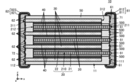
- FIG. 2 is a side sectional view showing the configuration of a solid electrolytic capacitor according to an embodiment of the present invention.
- FIG. 3 is an enlarged plan view of the end surface of the element body of the solid electrolyte capacitor where the anode electrode is exposed.
- FIG. 4 is a table showing the relationship between coverage and adhesion strength.
- FIG. 5 is a flowchart showing an example of a schematic flow of the method for manufacturing a solid electrolytic capacitor according to the present embodiment.
- 6(A), FIG. 6(B), and FIG. 6(C) are side sectional views of the solid electrolytic capacitor according to the present embodiment according to each process.
- FIG. 7 is a diagram of an apparatus for forming a conductive anchor member using the AD method.
- FIG. 8 is a table showing the relationship between the Young's modulus of the insulating resin and the film formability of the conductive anchor member.
- a solid electrolytic capacitor and a method for manufacturing a solid electrolytic capacitor according to a first embodiment of the present invention will be described with reference to the drawings.
- a chip-shaped capacitor has an element body made of insulating resin.
- the functional part of the capacitor is formed inside the element body.
- a chip-type capacitor has an electrode of a functional part of the capacitor exposed from an end surface of an element body, and has an external electrode formed on this exposed surface.
- FIG. 1 is an external perspective view of a solid electrolytic capacitor according to an embodiment of the present invention.
- FIG. 2 is a side sectional view showing the configuration of a solid electrolytic capacitor according to an embodiment of the present invention.
- FIG. 2 is a cross-sectional view taken along a plane perpendicular to the top, bottom, and end surfaces of the solid electrolytic capacitor body.
- FIG. 3 is an enlarged plan view of the end surface of the element body of the solid electrolyte capacitor where the anode electrode is exposed.
- the solid electrolytic capacitor 10 includes an element body 11, a conductive anchor member 61, a conductive anchor member 62, a resin electrode 71, a resin electrode 72, an external electrode 81, and an external electrode 82. .
- the element body 11 has a rectangular parallelepiped shape and has a top surface, a bottom surface, an end surface 111, an end surface 112, and two side surfaces.
- the end surface 111 corresponds to the "first end surface” of the present invention
- the end surface 112 corresponds to the "second end surface” of the present invention.
- the top surface and the bottom surface are used for convenience of explanation, and when a solid electrolytic capacitor is mounted on a circuit board, either surface may face the circuit board side.
- the element body 11 includes a plurality of capacitor elements 20, a plurality of cathode electrodes 30, a plurality of connection layers 40, an insulating resin 50, and an insulator layer 500.
- the capacitor element 20 includes an anode electrode 21, a dielectric layer 210, and a CP layer (solid electrolyte layer) 22.
- the anode electrode 21 has a flat film shape and has a first end surface, a second end surface, and a flat film surface.
- the anode electrode 21 is made of aluminum, for example.
- the anode electrode 21 includes an etching layer 21E consisting of a large number of holes recessed from the flat membrane surface. As a result, a portion of the anode electrode 21 having a predetermined thickness near the flat membrane surface is a porous body.
- the ratio of the thicknesses of the porous body and core metal portion on one side of the anode electrode 21 to the thickness of the porous body on the other side is about 1:1:1.
- the dielectric layer 210 covers the etching layer 21E of the anode electrode 21.
- the dielectric layer 210 is preferably made of an oxide film of the anode electrode 21 .
- the dielectric layer 210 is formed by oxidizing it in an aqueous solution containing boric acid, phosphoric acid, adipic acid, or a sodium salt or ammonium salt thereof.
- the thickness of the dielectric layer 210 is preferably 10 nm or more and 100 nm or less.
- illustration of the detailed structure of the anode electrode 21 is omitted, so the dielectric layer 210 is schematically illustrated as covering the macroscopic surface (flat membrane surface) of the anode electrode 21. .
- the dielectric layer 210 covers not only the macroscopic surface (flat membrane surface) of the anode electrode 21 but also the inner surfaces of many holes present in the etched layer 21E of the anode electrode 21.
- the CP layer 22 covers the surface of the dielectric layer 210.
- An insulator layer 500 is formed in a region of the flat membrane surface of the anode electrode 21 on the end surface 211 side.
- the region in which the CP layer 22 is formed is regulated by the insulator layer 500. More specifically, the CP layer 22 has a shape that does not reach the end surface 211 of the anode electrode 21.
- the anode electrode 21 and the CP layer 22 face each other with the dielectric layer 210 in between, and the capacitor element 20 functions as a capacitor having a predetermined capacitance.
- the plurality of capacitor elements 20 and the plurality of cathode electrodes 30 have a flat film shape.
- the plurality of capacitor elements 20 and the plurality of cathode electrodes 30 are arranged such that their respective flat membrane surfaces are substantially parallel to the top and bottom surfaces of the element body 11.
- the plurality of capacitor elements 20 and the plurality of cathode electrodes 30 are arranged alternately in a direction perpendicular to the top surface and the bottom surface (height direction of the element body 11 (z-axis direction in the figure)). Note that in FIG. 2, the number of the plurality of capacitor elements 20 is three, and the number of the plurality of cathode electrodes 30 is four, but the number is not limited to this.
- connection layer 40 is provided between adjacent capacitor elements 20 and cathode electrodes 30.
- the connection layer 40 has conductivity. Thereby, the CP layer 22 and the cathode electrode 30 of the capacitor element 20 are electrically connected.
- the end surfaces 211 (see FIG. 2) of the plurality of capacitor elements 20 are at approximately the same position when viewed from the side.
- the end surfaces 311 of the plurality of cathode electrodes 30 are at approximately the same position when viewed from the side.
- the end surfaces 211 of the plurality of capacitor elements 20 protrude from the end surfaces 312 of the plurality of cathode electrodes 30.
- the end surfaces 311 of the plurality of cathode electrodes 30 protrude more than the end surfaces 212 of the plurality of capacitor elements 20.
- the capacitor laminate in which a plurality of capacitor elements 20 and a plurality of cathode electrodes 30 are stacked in this way is sealed with an insulating resin 50. More specifically, the insulating resin 50 covers the capacitor laminate so that the end faces 211 of the plurality of capacitor elements 20 and the end faces 311 of the plurality of cathode electrodes 30 are exposed and the other parts are enclosed.
- the insulating resin 50 is preferably made of, for example, epoxy resin, phenol resin, polyimide resin, silicone resin, polyamide resin, liquid crystal polymer, or the like.
- the end faces 211 of the plurality of capacitor elements 20 are exposed to the outside of the element body 11 from the end face 111 of the element body 11. Furthermore, the end faces 311 of the plurality of cathode electrodes 30 are exposed to the outside of the element body 11 from the end face 112 of the element body 11 .
- the conductive anchor members 61 and 62 are a group of particles made of a conductive material.
- the conductive anchor members 61 and 62 are preferably made of metal, and more preferably contain at least one of copper, nickel, tin, and zinc, from the viewpoint of conductivity and formation method described below.
- the conductive anchor member 61 is formed on the end surface 111 of the element body 11. More specifically, the conductive anchor member 61 is formed on the end surface 211 of the anode electrode 21 of the plurality of capacitor elements 20. The conductive anchor member 61 is formed with a predetermined thickness (height) from the end surface 211. That is, the conductive anchor member 61 protrudes outward from the end surface 111 of the element body 11.
- the conductive anchor member 61 is formed on the surface of the insulating resin 50 on the end face 111 of the element body 11 at a predetermined coverage rate (details will be described later).
- the coverage is expressed as a ratio (percentage) of the area covered by the conductive anchor member 61 to the surface area of the insulating resin 50 on the end face 111 of the element body 11.
- the coverage rate is calculated as follows. First, in the solid electrolytic capacitor 10 shown in FIG. 2, the end surface 111 of the insulating resin 50 on which the conductive anchor member 61 is formed is exposed. After that, it can be determined by observing with an optical microscope and analyzing the obtained image. That is, the area of the insulating resin 50 portion and the area of the conductive anchor member 61 are calculated by binarizing the obtained image and distinguishing between the two. Then, the coverage is calculated as the ratio of the area of the conductive anchor member 61 to the sum of the area of the insulating resin 50 and the area of the conductive anchor member 61.
- the conductive anchor member 61 has a portion protruding from the surface of the insulating resin 50. Furthermore, it is preferable that the surface formed by the conductive anchor member 61 has irregularities.
- the conductive anchor member 62 is formed on the end surface 112 of the element body 11. More specifically, the conductive anchor member 62 is formed on the end surface 311 of the cathode electrode 30 of the plurality of capacitor elements 20. The conductive anchor member 62 is formed with a predetermined thickness (height) from the end surface 311. That is, the conductive anchor member 62 protrudes outward from the end surface 112 of the element body 11 .
- the conductive anchor member 62 is formed on the surface of the insulating resin 50 on the end face 112 of the element body 11 at a predetermined coverage rate (details will be described later).
- the coverage is expressed as a ratio (percentage) of the area covered by the conductive anchor member 62 to the surface area of the insulating resin 50 on the end face 112 of the element body 11.
- the coverage can be determined in the same manner as in the case of the conductive anchor member 61.
- the conductive anchor member 62 has a portion protruding from the surface of the insulating resin 50. Furthermore, it is preferable that the surface formed by the conductive anchor member 62 has irregularities.
- the resin electrode 71 contacts the end surface 111 of the element body 11 and the conductive anchor member 61, and covers the end surface 111 and the conductive anchor member 61.
- the resin electrode 72 contacts the end surface 112 of the element body 11 and the conductive anchor member 62 , and covers the end surface 112 and the conductive anchor member 62 .
- the external electrode 81 has a laminated structure of an electrode film 811 and an electrode film 812. Electrode film 811 covers the outer surface of resin electrode 71. Electrode film 812 covers the outer surface of electrode film 811.
- the external electrode 82 has a laminated structure of an electrode film 821 and an electrode film 822. The electrode film 821 covers the outer surface of the resin electrode 72. Electrode film 822 covers the outer surface of electrode film 821.
- the resin electrode 71 and the external electrode 81 constitute the "first external electrode” of the present invention.
- the resin electrode 72 and the external electrode 82 constitute the "second external electrode” of the present invention.
- FIG. 4 is a table showing the relationship between coverage and adhesion strength.
- the adhesion strength shown in FIG. 4 is the adhesion strength between the element body 11 and the resin electrode 71.
- Adhesion strength NL indicates a state of having a certain degree of adhesion.
- Adhesion strength GD indicates a state in which adhesion is strong enough to reliably obtain desired reliability in actual use.
- the adhesion strength VG indicates a state in which the adhesion strength is higher than the adhesion strength GD.
- FIG. 4 is a table showing the relationship between the coverage rate and adhesion strength described above.
- the coverage ratio is the ratio of the surface area of the insulating resin 50 on the end surface 111 of the element body 11 covered by the conductive anchor member 61, as described above.
- the adhesion strength indicates the degree of adhesion between the element body 11 and the resin electrode 71.
- NL, GD, and VG in FIG. 4 qualitatively represent the degree of close contact. That is, NL indicates a state of having a certain degree of adhesion.
- GD indicates a state in which the adhesive has adhesion strength that ensures desired reliability in actual use.
- VG indicates a state with even higher adhesion than the GD state.
- the coverage is 10% or more, desired reliability can be reliably obtained in actual use. If the coverage is 20% or more, even higher adhesion can be achieved more reliably.
- the coverage is set to 10% or more, and more preferably, the coverage is set to 20% or more.
- the solid electrolytic capacitor 10 can obtain high adhesion between the element body and the external electrode, and can realize high reliability.
- FIG. 5 is a flowchart showing an example of a schematic flow of the method for manufacturing a solid electrolytic capacitor according to the present embodiment.
- 6(A), FIG. 6(B), and FIG. 6(C) are side sectional views of the solid electrolytic capacitor according to the present embodiment according to each process.
- FIG. 7 is a diagram of an apparatus for forming a conductive anchor member using the AD method.
- the element body 11 is formed (S11). Specifically, as shown in FIG. 6A, a plurality of capacitor elements 20 and a plurality of cathode electrodes 30 are sequentially stacked with a connection layer 40 in between to form a laminate.
- the element body 11 is formed by sealing the laminate with an insulating resin 50.
- the anode electrodes 21 and the cathode electrodes 30 of the plurality of capacitor elements 20 are made of, for example, aluminum.
- the solid electrolyte layers of the plurality of capacitor elements 20 are made of, for example, a conductive polymer.
- the insulating resin 50 is made by applying and curing a predetermined insulating resin material.
- a conductive anchor member 61 is formed on the end surface 211 of the anode electrode 21 of the plurality of capacitor elements 20 in the element body 11 using the AD method (S12).
- a plurality of element bodies 11 are fixed on a stage 92 and placed in a chamber 91. At least the tip (the ejection end) of the aerosol generator 93 is inserted into the chamber 91 .
- the aerosol generator 93 generates an aerosol by introducing copper powder (Cu powder) 600 into the carrier gas, and sprays the aerosol onto the end surface 111 of the element body 11 .
- the copper powder 600 can be They are struck against the end surface 111 of the body 11 and piled up at a predetermined height (predetermined thickness).
- the conductive anchor member 61 is formed on the end surface 211 of the anode electrode 21 on the end surface 111 of the element body 11 and on the surface of the insulating resin 50 (see FIG. 6(B)).
- the particle size of the copper powder 600 is, for example, about 3 ⁇ m, but may be 2 ⁇ m or less.
- the AD method a part of the copper powder forming the conductive anchor member 61 bites into the surface of the insulating resin 50, and a predetermined anchor effect is achieved. Furthermore, by using the AD method, additional copper powder can be easily laminated on the copper powder that has bitten into the surface of the insulating resin 50. Furthermore, by using the AD method, the thickness of the conductive anchor member 61 can be controlled and unevenness can be formed on its surface. This further improves the anchor effect.
- conductive anchor members 62 are formed on the end faces 311 of the plurality of cathode electrodes 30 in the element body 11 using the AD method (S13). Note that the method for forming the conductive anchor member 62 is the same as the method for forming the conductive anchor member 61, and a description thereof will be omitted (see FIG. 6(B)).
- the resin electrode 71 is formed so as to cover the end surface 111 of the element body 11 and the conductive anchor member 61. Furthermore, a resin electrode 72 is formed so as to cover the end surface 112 of the element body 11 and the conductive anchor member 62 (S15). Specifically, the resin electrode 71 is made of a paste-like material in which conductive particles such as silver (Ag) are kneaded into resin. The resin electrode 71 is formed by applying this paste-like material so as to cover the end surface 111 of the element body 11 and the conductive anchor member 61 and then solidifying it (see FIG. 6(C)). The resin electrode 72 is also formed by the same method as the resin electrode 71, so a description thereof will be omitted (see FIG. 6(C)).
- an external electrode 81 is formed on the surface of the resin electrode 71, and an external electrode 82 is formed on the surface of the resin electrode 72 (S15).
- the external electrode 81 consists of an electrode film 811 and an electrode film 812, and is formed by plating.
- the electrode film 811 is a nickel (Ni) plating layer
- the electrode film 812 is a tin (Sn) plating layer.
- the external electrode 82 is also formed by plating like the external electrode 81.
- the electrode film 821 is a nickel (Ni) plating layer
- the electrode film 822 is a tin (Sn) plating layer.
- the thickness of the terminal electrode consisting of the resin electrode 71 and the external electrode 81 and the thickness of the terminal electrode consisting of the resin electrode 72 and the external electrode 82 are preferably 8 ⁇ m or more and less than 20 ⁇ m.
- the solid electrolytic capacitor 10 having the above configuration can be manufactured easily and more reliably.
- a solid electrolytic capacitor according to a second embodiment of the present invention will be described with reference to the drawings.
- the solid electrolytic capacitor according to the second embodiment is similar to the solid electrolytic capacitor 10 according to the first embodiment in that the material of the insulating resin 50 is specified.
- the other configuration of the solid electrolytic capacitor according to the second embodiment is the same as that of the solid electrolytic capacitor according to the first embodiment, and a description of the similar parts will be omitted.
- FIG. 8 is a table showing the relationship between the Young's modulus of the insulating resin and the film formability of the conductive anchor member.
- film formability NG indicates a state in which the conductive anchor members 61 and 62 can hardly be formed on the surface of the insulating resin 50.
- Film formability GD indicates a state in which the above-described conductive anchor members 61 and 62 can be formed on the surface of the insulating resin 50.
- Film formability VG indicates a state in which the conductive anchor members 61 and 62 can be formed into films more reliably than film formability GD.
- the Young's modulus of the insulating resin 50 was determined from a separately prepared test piece made of the same material.
- the Young's modulus can be determined by measuring the test piece using a method and device that comply with the JIS plastic bending standard (JIS K 7171) or the plastic tensile standard (JIS K 7161), and analyzing the obtained data. Calculated.
- the Young's modulus when the Young's modulus is 9.0 or more, the desired film formability of the conductive anchor members 61 and 62 on the surface of the insulating resin 50 can be ensured. Furthermore, when the Young's modulus is 12 or more, the desired film forming properties of the conductive anchor members 61 and 62 on the surface of the insulating resin 50 can be more reliably ensured.
- the solid electrolytic capacitor 10 can achieve high reliability. Furthermore, by setting the Young's modulus of the insulating resin 50 to 12.0 or more, the bonding strength between the element body 11 and the resin electrodes 71 and 72 is further improved, and the solid electrolytic capacitor 10 can achieve higher reliability. .
- Conductive anchor members 61 and 62 can be formed at desired heights on the end surface 211 of the anode electrode 21 and the end surface 311 of the cathode electrode 30. As a result, the electrical and physical connection between the anode electrode 21 and the resin electrode 71 and the electrical and physical connection between the cathode electrode 30 and the resin electrode 72 can be ensured in no small part.
- the cathode electrode 30 is used, but the cathode electrode 30 can be omitted.
- the solid electrolytic capacitor may employ the above-described configuration at least on the end surface 111 (the surface where the anode electrode 21 is exposed).
- the resin electrodes 71 and 72 can also be omitted.
- the external electrode 81 is directly formed on the end surface 111 of the element body 11 after the conductive anchor member 61 is formed. Furthermore, after the conductive anchor member 62 is formed on the end surface 112, the external electrode 82 is directly formed thereon.
- An element body including an element laminate in which a plurality of capacitor elements are stacked, and an insulating resin covering the element laminate; an external electrode formed on the element body; Equipped with The element body has a first end surface where electrodes of the plurality of capacitor elements are exposed, the external electrode is formed on the first end surface, A conductive anchor member is formed on the first end surface on the exposed surface of the electrode of the capacitor element and on the surface of the insulating resin, A capacitor, wherein a coverage of the surface of the insulating resin on the first end surface by the conductive anchor member is 10% or more.
- ⁇ 2> The capacitor of ⁇ 1>, wherein the coverage is 20% or more.
- the plurality of capacitor elements are an anode electrode made of a flat membrane-like valve metal body; a dielectric layer formed on the anode electrode; a solid electrolyte layer covering the dielectric layer; A ⁇ 1> or ⁇ 2> capacitor comprising:
- the element body has a second end face that faces the first end face and exposes the plurality of cathode electrodes
- the external electrode includes a first external electrode formed on the first end surface and a second external electrode formed on the second end surface, On the second end surface, a conductive anchor member is formed on the exposed surface of the cathode electrode and the surface of the insulating resin,
- ⁇ 6> The capacitor according to any one of ⁇ 1> to ⁇ 5>, wherein the conductive anchor member is made of at least one of copper, nickel, tin, and zinc.
- ⁇ 7> The capacitor according to any one of ⁇ 1> to ⁇ 6>, wherein the insulating resin has a Young's modulus of 9.0 or more.
- the external electrode is a resin electrode connected to the electrodes of the plurality of capacitor elements and the insulating resin via the conductive anchor member; a plating electrode covering the resin electrode; Equipped with Any one of the capacitors ⁇ 1> to ⁇ 7>.
- Solid electrolytic capacitor 11 Element body 20: Capacitor element 21: Anode electrode 21E: Etching layer 22: CP layer 30: Cathode electrode 40: Connection layer 50: Insulating resin 61, 62: Conductive anchor member 71, 72: Resin electrodes 81, 82: External electrode 91: Chamber 92: Stage 93: Aerosol generators 111, 112: End face 210: Dielectric layer 211, 212, 311, 312: End face 500: Insulator layer 600: Copper powder 811, 812 , 821, 822: electrode film
Landscapes
- Engineering & Computer Science (AREA)
- Power Engineering (AREA)
- Microelectronics & Electronic Packaging (AREA)
- Manufacturing & Machinery (AREA)
- Fixed Capacitors And Capacitor Manufacturing Machines (AREA)
Priority Applications (2)
| Application Number | Priority Date | Filing Date | Title |
|---|---|---|---|
| CN202380058831.1A CN119856239A (zh) | 2022-08-29 | 2023-05-16 | 电容器以及电容器的制造方法 |
| JP2024543785A JPWO2024047961A1 (https=) | 2022-08-29 | 2023-05-16 |
Applications Claiming Priority (2)
| Application Number | Priority Date | Filing Date | Title |
|---|---|---|---|
| JP2022-135526 | 2022-08-29 | ||
| JP2022135526 | 2022-08-29 |
Publications (1)
| Publication Number | Publication Date |
|---|---|
| WO2024047961A1 true WO2024047961A1 (ja) | 2024-03-07 |
Family
ID=90099314
Family Applications (1)
| Application Number | Title | Priority Date | Filing Date |
|---|---|---|---|
| PCT/JP2023/018285 Ceased WO2024047961A1 (ja) | 2022-08-29 | 2023-05-16 | コンデンサ、およびコンデンサの製造方法 |
Country Status (3)
| Country | Link |
|---|---|
| JP (1) | JPWO2024047961A1 (https=) |
| CN (1) | CN119856239A (https=) |
| WO (1) | WO2024047961A1 (https=) |
Cited By (1)
| Publication number | Priority date | Publication date | Assignee | Title |
|---|---|---|---|---|
| WO2026028974A1 (ja) * | 2024-07-30 | 2026-02-05 | パナソニックIpマネジメント株式会社 | 固体電解コンデンサ |
Citations (5)
| Publication number | Priority date | Publication date | Assignee | Title |
|---|---|---|---|---|
| WO2013128957A1 (ja) * | 2012-02-29 | 2013-09-06 | 株式会社村田製作所 | 導電性ペースト、及び電子部品、並びに電子部品の製造方法 |
| WO2020174847A1 (ja) * | 2019-02-28 | 2020-09-03 | 株式会社村田製作所 | 電子部品及び電子部品の製造方法 |
| WO2022168768A1 (ja) * | 2021-02-02 | 2022-08-11 | 株式会社村田製作所 | 電子部品の製造方法 |
| WO2022168770A1 (ja) * | 2021-02-02 | 2022-08-11 | 株式会社村田製作所 | 電解コンデンサ |
| WO2022168769A1 (ja) * | 2021-02-02 | 2022-08-11 | 株式会社村田製作所 | 電解コンデンサ及び電解コンデンサの製造方法 |
-
2023
- 2023-05-16 WO PCT/JP2023/018285 patent/WO2024047961A1/ja not_active Ceased
- 2023-05-16 JP JP2024543785A patent/JPWO2024047961A1/ja active Pending
- 2023-05-16 CN CN202380058831.1A patent/CN119856239A/zh active Pending
Patent Citations (5)
| Publication number | Priority date | Publication date | Assignee | Title |
|---|---|---|---|---|
| WO2013128957A1 (ja) * | 2012-02-29 | 2013-09-06 | 株式会社村田製作所 | 導電性ペースト、及び電子部品、並びに電子部品の製造方法 |
| WO2020174847A1 (ja) * | 2019-02-28 | 2020-09-03 | 株式会社村田製作所 | 電子部品及び電子部品の製造方法 |
| WO2022168768A1 (ja) * | 2021-02-02 | 2022-08-11 | 株式会社村田製作所 | 電子部品の製造方法 |
| WO2022168770A1 (ja) * | 2021-02-02 | 2022-08-11 | 株式会社村田製作所 | 電解コンデンサ |
| WO2022168769A1 (ja) * | 2021-02-02 | 2022-08-11 | 株式会社村田製作所 | 電解コンデンサ及び電解コンデンサの製造方法 |
Cited By (1)
| Publication number | Priority date | Publication date | Assignee | Title |
|---|---|---|---|---|
| WO2026028974A1 (ja) * | 2024-07-30 | 2026-02-05 | パナソニックIpマネジメント株式会社 | 固体電解コンデンサ |
Also Published As
| Publication number | Publication date |
|---|---|
| CN119856239A (zh) | 2025-04-18 |
| JPWO2024047961A1 (https=) | 2024-03-07 |
Similar Documents
| Publication | Publication Date | Title |
|---|---|---|
| US6400556B1 (en) | Solid electrolytic capacitor and method of fabricating the same | |
| CN107026019A (zh) | 固体电解电容器 | |
| WO2008007491A1 (ja) | 積層型電子部品及び積層型アレイ電子部品 | |
| TWI378482B (en) | Solid electrolytic capacitor element and solid electrolytic capacitor | |
| US12456586B2 (en) | Electrolytic capacitor | |
| US20150077905A1 (en) | Solid electrolytic capacitor | |
| US7085127B2 (en) | Surface mount chip capacitor | |
| WO2021085555A1 (ja) | 電解コンデンサ | |
| WO2022163644A1 (ja) | 電解コンデンサ | |
| WO2024047961A1 (ja) | コンデンサ、およびコンデンサの製造方法 | |
| CN217214477U (zh) | 电子组件封装结构及半成品组合体 | |
| US12374505B2 (en) | Electrolytic capacitor | |
| CN104137204B (zh) | 固体电解电容器 | |
| JPH0684716A (ja) | 固体電解コンデンサの製造方法 | |
| JP2002110458A (ja) | チップ状固体電解コンデンサ | |
| JP2002110459A (ja) | チップ状固体電解コンデンサ | |
| JPH0448616A (ja) | 固体電解コンデンサおよびその製造方法 | |
| JP7794325B2 (ja) | 固体電解コンデンサ、および固体電解コンデンサの製造方法 | |
| TWI339401B (https=) | ||
| JP2010278203A (ja) | 積層型固体電解コンデンサおよびその製造方法 | |
| WO2023243581A1 (ja) | コンデンサの製造方法、および、コンデンサ | |
| WO2022181606A1 (ja) | フィルタ回路 | |
| WO2024247449A1 (ja) | 固体電解コンデンサ、および固体電解コンデンサの製造方法 | |
| JP5371865B2 (ja) | 3端子型コンデンサ | |
| WO2004084243A1 (ja) | コンデンサ素子、固体電解コンデンサ及びそれらの製造方法並びにコンデンサ素子結合体 |
Legal Events
| Date | Code | Title | Description |
|---|---|---|---|
| 121 | Ep: the epo has been informed by wipo that ep was designated in this application |
Ref document number: 23859731 Country of ref document: EP Kind code of ref document: A1 |
|
| WWE | Wipo information: entry into national phase |
Ref document number: 2024543785 Country of ref document: JP |
|
| WWE | Wipo information: entry into national phase |
Ref document number: 202380058831.1 Country of ref document: CN |
|
| NENP | Non-entry into the national phase |
Ref country code: DE |
|
| WWP | Wipo information: published in national office |
Ref document number: 202380058831.1 Country of ref document: CN |
|
| 122 | Ep: pct application non-entry in european phase |
Ref document number: 23859731 Country of ref document: EP Kind code of ref document: A1 |