WO2024043008A1 - 半導体装置 - Google Patents
半導体装置 Download PDFInfo
- Publication number
- WO2024043008A1 WO2024043008A1 PCT/JP2023/027915 JP2023027915W WO2024043008A1 WO 2024043008 A1 WO2024043008 A1 WO 2024043008A1 JP 2023027915 W JP2023027915 W JP 2023027915W WO 2024043008 A1 WO2024043008 A1 WO 2024043008A1
- Authority
- WO
- WIPO (PCT)
- Prior art keywords
- electrode
- wiring
- thickness direction
- switching element
- semiconductor device
- Prior art date
- Legal status (The legal status is an assumption and is not a legal conclusion. Google has not performed a legal analysis and makes no representation as to the accuracy of the status listed.)
- Ceased
Links
Images









Classifications
-
- H—ELECTRICITY
- H10—SEMICONDUCTOR DEVICES; ELECTRIC SOLID-STATE DEVICES NOT OTHERWISE PROVIDED FOR
- H10W—GENERIC PACKAGES, INTERCONNECTIONS, CONNECTORS OR OTHER CONSTRUCTIONAL DETAILS OF DEVICES COVERED BY CLASS H10
- H10W70/00—Package substrates; Interposers; Redistribution layers [RDL]
- H10W70/40—Leadframes
- H10W70/481—Leadframes for devices being provided for in groups H10D8/00 - H10D48/00
-
- H—ELECTRICITY
- H10—SEMICONDUCTOR DEVICES; ELECTRIC SOLID-STATE DEVICES NOT OTHERWISE PROVIDED FOR
- H10W—GENERIC PACKAGES, INTERCONNECTIONS, CONNECTORS OR OTHER CONSTRUCTIONAL DETAILS OF DEVICES COVERED BY CLASS H10
- H10W90/00—Package configurations
-
- H—ELECTRICITY
- H10—SEMICONDUCTOR DEVICES; ELECTRIC SOLID-STATE DEVICES NOT OTHERWISE PROVIDED FOR
- H10W—GENERIC PACKAGES, INTERCONNECTIONS, CONNECTORS OR OTHER CONSTRUCTIONAL DETAILS OF DEVICES COVERED BY CLASS H10
- H10W90/00—Package configurations
- H10W90/811—Multiple chips on leadframes
-
- H—ELECTRICITY
- H10—SEMICONDUCTOR DEVICES; ELECTRIC SOLID-STATE DEVICES NOT OTHERWISE PROVIDED FOR
- H10W—GENERIC PACKAGES, INTERCONNECTIONS, CONNECTORS OR OTHER CONSTRUCTIONAL DETAILS OF DEVICES COVERED BY CLASS H10
- H10W90/00—Package configurations
- H10W90/701—Package configurations characterised by the relative positions of pads or connectors relative to package parts
- H10W90/751—Package configurations characterised by the relative positions of pads or connectors relative to package parts of bond wires
- H10W90/753—Package configurations characterised by the relative positions of pads or connectors relative to package parts of bond wires between laterally-adjacent chips
Definitions
- the present disclosure relates to a semiconductor device.
- Patent Document 1 discloses an example of a semiconductor device including a horizontally structured semiconductor element (HEMT).
- the semiconductor device described in Patent Document 1 includes a first semiconductor element, a second semiconductor element, and a control element.
- the first semiconductor element and the second semiconductor element are horizontally structured switching elements (HEMT).
- the control element controls driving of the first semiconductor element and the second semiconductor element.
- These first semiconductor element, second semiconductor element, and control element are mounted on a lead frame, and are arranged along the same plane (a plane including the x direction and y direction shown in FIGS. 1 and 2 of the same document). and are spaced apart from each other.
- the plane size is relatively large. This hinders miniaturization of semiconductor devices. Further, in the configuration of the conventional semiconductor device described above, the path of the conductive wiring (wire) for connecting the plurality of elements arranged along the same plane to each other is relatively long. This results in an increase in parasitic inductance in the wiring of the semiconductor device.
- An object of the present disclosure is to provide a semiconductor device that is improved over the conventional semiconductor device.
- one object of the present disclosure is to provide a semiconductor device suitable for miniaturization and reduction of parasitic inductance in wiring.
- a semiconductor device provided by one aspect of the present disclosure includes a first semiconductor element having a first main surface facing one side in the thickness direction, and a first semiconductor element having a first main surface facing one side in the thickness direction with respect to the first semiconductor element.
- the semiconductor device includes a wiring layer arranged therein, and a second semiconductor element arranged on one side in the thickness direction with respect to the wiring layer.
- the first semiconductor element has a first electrode, a second electrode, and a third electrode, each of which is formed on the first main surface.
- the second semiconductor element overlaps the first semiconductor element when viewed in the thickness direction.
- the second semiconductor element is electrically connected to the first semiconductor element via the wiring layer.
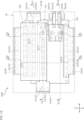
- FIG. 1 is a plan view showing a semiconductor device according to a first embodiment of the present disclosure.
- FIG. 2 is a plan view showing the semiconductor device according to the first embodiment of the present disclosure, through which the sealing part is seen.
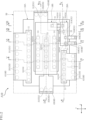
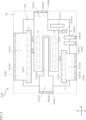
- FIG. 3 is a plan view corresponding to FIG. 2, in which a switching element (second semiconductor element), a control element (third semiconductor element), and a portion of a plurality of connection wirings are omitted.
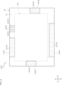
- FIG. 4 is a bottom view showing the semiconductor device according to the first embodiment of the present disclosure.
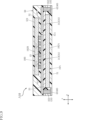
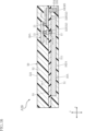
- FIG. 5 is a sectional view taken along line VV in FIG. 2.
- FIG. 6 is a cross-sectional view taken along line VI-VI in FIG.
- FIG. 7 is a cross-sectional view taken along line VII-VII in FIG.
- FIG. 5 is a sectional view taken along line VV in FIG. 2.
- FIG. 6 is a cross-sectional view taken along line VI-VI in FIG.
- FIG. 7 is a cross-sectional view
- FIG. 8 is a cross-sectional view taken along line VIII-VIII in FIG.
- FIG. 9 is a cross-sectional view taken along line IX-IX in FIG.
- FIG. 10 is a sectional view taken along line XX in FIG. 2.
- FIG. 11 is a cross-sectional view similar to FIG. 5, showing a semiconductor device according to a first modification of the first embodiment.
- FIG. 12 is a plan view showing a semiconductor device according to a second embodiment of the present disclosure.
- FIG. 13 is a sectional view taken along line XIII-XIII in FIG. 12.
- FIG. 14 is a sectional view taken along line XIV-XIV in FIG. 12.
- FIG. 15 is a sectional view taken along line XV-XV in FIG. 12.
- FIG. 16 is a cross-sectional view taken along line XVI-XVI in FIG. 12.
- FIG. 17 is a cross-sectional view similar to FIG. 14, showing a semiconductor device according to a first modification of the second embodiment.
- FIG. 18 is a plan view showing a semiconductor device according to a third embodiment of the present disclosure.
- FIG. 19 is a sectional view taken along line XIX-XIX in FIG. 18.
- FIG. 20 is a cross-sectional view taken along line XX-XX in FIG. 18.
- FIG. 21 is a cross-sectional view taken along line XXI-XXI in FIG. 18.
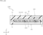
- FIG. 22 is a cross-sectional view taken along line XXII-XXII in FIG. 18.
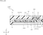
- FIG. 23 is a sectional view taken along line XXIII-XXIII in FIG. 18.
- a thing A is formed on a thing B and "a thing A is formed on a thing B” mean “a thing A is formed on a thing B” unless otherwise specified.
- "something A is placed on something B” and “something A is placed on something B” mean "something A is placed on something B” unless otherwise specified.
- a certain surface A faces (one side or the other side of) the direction B is not limited to the case where the angle of the surface A with respect to the direction B is 90 degrees; Including cases where it is tilted to the opposite direction.
- the semiconductor device A10 of this embodiment includes a switching element 10A, a switching element 10B, a control element 20A, a wiring layer 31, a plurality of connection wirings 34, a plurality of communication wirings 35, a plurality of terminals 40, and a sealing part 50.
- the semiconductor device A10 is in the form of a resin package that is surface mounted on a wiring board.
- FIG. 1 is a plan view showing the semiconductor device A10.
- FIG. 2 is a plan view showing the semiconductor device A10.
- FIG. 2 is a plan view showing the semiconductor device A10, through which the sealing portion 50 is seen. In FIG. 2, the transparent sealing portion 50 is shown by an imaginary line (two-dot chain line).
- FIG. 3 is a plan view of the semiconductor device A10, in which the switching element 10B, the control element 20A, and the portions of the plurality of connection wirings 34 connected to the switching element 10B and the control element 20A are omitted from FIG. .
- FIG. 4 is a bottom view showing the semiconductor device A10.
- FIG. 5 is a sectional view taken along line VV in FIG. 2.
- FIG. 6 is a cross-sectional view taken along line VI-VI in FIG.
- FIG. 7 is a cross-sectional view taken along line VII-VII in FIG.
- FIG. 8 is a cross-sectional view taken along line VIII-VIII in FIG.
- FIG. 9 is a cross-sectional view taken along line IX-IX in FIG.
- FIG. 10 is a sectional view taken along line XX in FIG. 2.
- the thickness direction z corresponds to the thickness direction of the semiconductor device A10.
- plane view refers to when viewed in the thickness direction z.
- the first direction x is orthogonal to the thickness direction z.
- the second direction y is orthogonal to the thickness direction z and the first direction x. Note that one side in the thickness direction z is referred to as the z1 side in the thickness direction z, and the other side in the thickness direction z is referred to as the z2 side in the thickness direction z.
- the z1 side in the thickness direction z may be referred to as the upper side, and the z2 side in the thickness direction z may be referred to as the lower side.
- descriptions such as “upper”, “lower”, “upper”, “lower”, “upper surface”, and “lower surface” indicate the relative positional relationship of each component etc. in the thickness direction z, and do not necessarily mean It is not a term that defines the relationship with the direction of gravity.
- the semiconductor device A10 has a rectangular shape when viewed in the thickness direction z.
- the semiconductor device A10 converts DC power supplied to the semiconductor device A10 from the outside into AC power using the switching element 10A and the switching element 10B.
- the semiconductor device A10 is used, for example, as an inverter for driving a motor.
- the wiring structure including the wiring layer 31 and the connection wiring 34 of the semiconductor device A10 can be formed by, for example, a redistribution layer (RDL) formation method using patterning and plating.
- RDL redistribution layer
- the sealing part 50 covers at least part of the switching element 10A and the switching element 10B, the control element 20A, the wiring layer 31, the plurality of connection wirings 34, the plurality of communication wirings 35, and a part of the plurality of terminals 40, respectively.
- the sealing portion 50 includes, for example, an insulating resin material.
- the sealing portion 50 has a rectangular shape when viewed in the thickness direction z.
- the sealing section 50 includes a first sealing section 51, a second sealing section 52, and a third sealing section 53.
- the first sealing part 51 is located on the z2 side in the thickness direction z in the sealing part 50.
- the first sealing part 51 has a bottom surface 511.
- the bottom surface 511 faces the z2 side in the thickness direction z.
- the bottom surface 511 faces the wiring board.
- the second sealing part 52 is arranged on the z1 side in the thickness direction z with respect to the first sealing part 51.
- the second sealing part 52 has a top surface 521.
- the top surface 521 faces the opposite side to the bottom surface 511 in the thickness direction z (the z1 side in the thickness direction z).
- the third sealing part 53 is located between the first sealing part 51 and the second sealing part 52 in the thickness direction z.
- the third sealing section 53 is in contact with the first sealing section 51 and the second sealing section 52, respectively.
- the switching element 10A and the switching element 10B are transistors (switching elements) mainly used for power conversion.
- Each of switching elements 10A and 10B is made of a material containing, for example, a nitride semiconductor.
- each of the switching elements 10A and 10B is a HEMT (High Electron Mobility Transistor) made of a material containing gallium nitride (GaN).
- the switching element 10A includes a first main surface 101A, a first back surface 102A, a plurality (two) of first electrodes 11, and a plurality (two) of first electrodes 11. It has two electrodes 12 and a third electrode 13.
- the first main surface 101A faces the z1 side in the thickness direction z.
- the first back surface 102A is separated from the first main surface 101A in the thickness direction z.
- the first back surface 102A faces the side opposite to the first main surface 101A (the z2 side in the thickness direction z).
- the plurality of first electrodes 11, the plurality of second electrodes 12, and the third electrode 13 are formed on the first main surface 101A.
- each of the plurality of (two) first electrodes 11 and the plurality of (two) second electrodes 12 extends in the first direction x.
- the two first electrodes 11 are located on both sides of the switching element 10A in the second direction y.
- the two second electrodes 12 are located between the two first electrodes 11 in the second direction y.
- the two second electrodes 12 are spaced apart from each other in the second direction y.
- a current corresponding to the power before being converted by the switching element 10A flows through the plurality of second electrodes 12. Therefore, the plurality of second electrodes 12 correspond to the drain of the switching element 10A.
- a current corresponding to the power converted by the switching element 10A flows through the plurality of first electrodes 11. Therefore, the plurality of first electrodes 11 correspond to the source of the switching element 10A.
- the third electrode 13 is arranged near the end of the switching element 10A in the first direction x and near the end in the second direction y.
- a gate voltage for driving the switching element 10A is applied to the third electrode 13.
- This third electrode 13 corresponds to the gate of the switching element 10A.
- the area of the third electrode 13 is smaller than the area of each of the plurality of first electrodes 11 and the plurality of second electrodes 12 when viewed in the thickness direction z.
- the shape, quantity, and arrangement of each of the first electrode 11, second electrode 12, and third electrode 13 in the switching element 10A are merely examples, and various changes are possible.
- the switching element 10A having the above configuration is an example of the "first semiconductor element" of the present disclosure.
- the switching element 10A is covered by the first sealing portion 51.
- a portion of the switching element 10A other than the first main surface 101A is covered with the first sealing portion 51. Therefore, the first back surface 102A is covered with the first sealing part 51.
- the first main surface 101A is in contact with the third sealing portion 53.
- the plurality of first electrodes 11 , the plurality of second electrodes 12 , and the third electrode 13 face the third sealing part 53 .
- the switching element 10B is arranged on the z1 side in the thickness direction z with respect to the switching element 10A.
- the switching element 10B overlaps the switching element 10A when viewed in the thickness direction z.
- the area of the switching element 10B is smaller than the area of the switching element 10A when viewed in the thickness direction z.
- FIG. 2 As shown in FIG. 2, FIG. 5, FIG. 8, and FIG. It has an electrode 16.
- the second main surface 101B faces the z2 side in the thickness direction z.
- the second main surface 101B faces the first main surface 101A of the switching element 10A.
- the second back surface 102B is separated from the second main surface 101B in the thickness direction z.
- the second back surface 102B faces the opposite side to the second main surface 101B (the z1 side in the thickness direction z).
- the plurality of fourth electrodes 14, fifth electrodes 15, and sixth electrodes 16 are formed on the second main surface 101B.
- each of the plurality of (two) fourth electrodes 14 and fifth electrode 15 extends in the first direction x.
- the two fourth electrodes 14 are located on both sides of the switching element 10B in the second direction y. Further, as understood from FIGS. 2, 3, 5, and 6, the two fourth electrodes 14 correspond to the two second electrodes 12 of the switching element 10A, respectively, when viewed in the thickness direction z. are individually overlapped.
- the fifth electrode 15 is located between the two fourth electrodes 14 in the second direction y. A current corresponding to the power before being converted by the switching element 10B flows through the fifth electrode 15. Therefore, the fifth electrode 15 corresponds to the drain of the switching element 10B. A current corresponding to the power converted by the switching element 10B flows through the plurality of fourth electrodes 14. Therefore, the plurality of fourth electrodes 14 correspond to the source of the switching element 10B.
- the sixth electrode 16 is arranged near the end of the switching element 10B in the first direction x and near the end in the second direction y.
- a gate voltage for driving the switching element 10B is applied to the sixth electrode 16.
- This sixth electrode 16 corresponds to the gate of the switching element 10B.
- the area of the sixth electrode 16 is smaller than the area of each of the plurality of fourth electrodes 14 and the fifth electrode 15 when viewed in the thickness direction z.
- the switching element 10B is electrically connected to the switching element 10A via the wiring layer 31.
- the shape, quantity, and arrangement of the fourth electrode 14, fifth electrode 15, and sixth electrode 16 in the switching element 10B are merely examples, and various changes are possible.
- the switching element 10B having the above configuration is an example of the "second semiconductor element" of the present disclosure.
- the switching element 10B is covered by the second sealing portion 52.
- the entire switching element 10B is covered with the second sealing part 52.
- the semiconductor device A10 is configured, for example, as a half-bridge switching circuit.
- the switching element 10B constitutes an upper arm circuit of the semiconductor device A10
- the switching element 10A constitutes a lower arm circuit. Switching element 10B and switching element 10A are connected in series.
- the control element 20A is arranged on the z1 side in the thickness direction z with respect to the switching element 10A.
- the control element 20A overlaps the switching element 10A when viewed in the thickness direction z.
- the area of the control element 20A is smaller than the area of each of the switching element 10A and the switching element 10B.
- the control element 20A is electrically connected to the switching element 10A and the switching element 10B.
- the control element 20A is a gate driver that applies a gate voltage to the third electrode 13 of the switching element 10A and the sixth electrode 16 of the switching element 10B.
- the control element 20A has a third main surface 201A and a plurality of (four) pads 21.
- the third main surface 201A faces the z2 side in the thickness direction z.
- the third main surface 201A faces the first main surface 101A of the switching element 10A.
- the plurality of pads 21 are formed on the third main surface 201A.
- each of the plurality of pads 21 has a rectangular shape when viewed in the thickness direction.
- the shape, quantity, and arrangement of the plurality of pads 21 in the control element 20A are merely examples, and various changes are possible.
- the control element 20A having the above configuration is an example of the "third semiconductor element" of the present disclosure.
- the wiring layer 31 is located between the switching element 10A, the switching element 10B, and the control element 20A in the thickness direction z. Thereby, the wiring layer 31 is arranged on the z1 side in the thickness direction z with respect to the switching element 10A. Further, the switching element 10B and the control element 20A are arranged on the z1 side in the thickness direction z with respect to the wiring layer 31.
- the wiring layer 31 is located between the third sealing part 53 and the second sealing part 52. At least a portion of the wiring layer 31 is accommodated in the second sealing section 52.
- the constituent material of the wiring layer 31 is not particularly limited, and includes copper (Cu), for example.
- the wiring layer 31 includes a first wiring 311, a second wiring 312, a third wiring 313, a fourth wiring 314, a fifth wiring 315, and a control wiring 316.
- the first wiring 311 is provided at two locations separated from each other.
- the two first wirings 311 are arranged corresponding to the plurality (two) of first electrodes 11 of the switching element 10A.
- Each first wiring 311 overlaps with the first electrode 11 when viewed in the thickness direction z.
- each first electrode 11 of the switching element 10A is electrically connected to the first wiring 311 via one of the plurality of connection wirings 34.
- the second wiring 312 is arranged in a bifurcated shape corresponding to the plurality (two) of second electrodes 12 of the switching element 10A and the plurality (two) of the fourth electrodes 14 of the switching element 10B.
- the second wiring 312 overlaps with the plurality of second electrodes 12 and the plurality of fourth electrodes 14 when viewed in the thickness direction z.
- each second electrode 12 of the switching element 10A is electrically connected to the second wiring 312 via one of the plurality of connection wirings 34.
- each fourth electrode 14 of the switching element 10B is electrically connected to the second wiring 312 via one of the plurality of connection wirings 34. That is, the fourth electrode 14 of the switching element 10B is electrically connected to the second electrode 12 of the switching element 10A via the wiring layer 31 (second wiring 312).
- the third wiring 313 is arranged corresponding to the fifth electrode 15 of the switching element 10B.
- the third wiring 313 overlaps with the fifth electrode 15 when viewed in the thickness direction z.
- the fifth electrode 15 is electrically connected to the third wiring 313 via one of the plurality of connection wirings 34.
- the fourth wiring 314 is arranged to correspond to either the third electrode 13 of the switching element 10A or the plurality of pads 21 of the control element 20A.
- the fourth wiring 314 overlaps with the third electrode 13 and any one of the plurality of pads 21 when viewed in the thickness direction z.
- the third electrode 13 is electrically connected to the fourth wiring 314 via one of the plurality of connection wirings 34.
- any one of the plurality of pads 21 is electrically connected to the fourth wiring 314 via one of the plurality of connection wirings 34.
- the control element 20A (any one of the plurality of pads 21) is electrically connected to the third electrode 13 via the fourth wiring 314.
- the pad 21 electrically connected to the fourth wiring 314 via the fourth wiring 314 overlaps with the third electrode 13 when viewed in the thickness direction z.
- the fifth wiring 315 is arranged corresponding to the sixth electrode 16 of the switching element 10B and one of the plurality of pads 21 of the control element 20A.
- the fifth wiring 315 overlaps with the sixth electrode 16 and any one of the plurality of pads 21 when viewed in the thickness direction z.
- the sixth electrode 16 is electrically connected to the fifth wiring 315 via one of the plurality of connection wirings 34.
- any one of the plurality of pads 21 is electrically connected to the fifth wiring 315 via one of the plurality of connection wirings 34.
- the control element 20A (any one of the plurality of pads 21) is electrically connected to the sixth electrode 16 via the fifth wiring 315.
- the control wiring 316 is arranged corresponding to one of the plurality of pads 21 of the control element 20A.
- the control wiring 316 is provided at two locations separated from each other.
- the two control wirings 316 are arranged corresponding to the two pads 21 of the control element 20A.
- Each control wiring 316 overlaps the pad 21 when viewed in the thickness direction z.
- each of the two pads 21 is electrically connected to the control wiring 316 via one of the plurality of connection wirings 34.
- the plurality of connection wirings 34 are accommodated in either the second sealing section 52 or the third sealing section 53. As shown in FIGS. 2 and 3, each of the plurality of connection wirings 34 overlaps with one of the switching element 10A, the switching element 10B, and the control element 20A when viewed in the thickness direction z. Each of the plurality of connection wirings 34 is connected to the wiring layer 31 (any one of the first wiring 311, the second wiring 312, the third wiring 313, the fourth wiring 314, the fifth wiring 315, and the control wiring 316).
- the plurality of connection wires 34 include a plurality of first connection wires 341, a plurality of second connection wires 342, and a plurality of third connection wires 343.
- the plurality of first connection wirings 341 are interposed between the switching element 10A and the wiring layer 31 in the thickness direction z.
- the plurality of first connection wirings 341 are accommodated in the third sealing portion 53.
- Each of the plurality of first connection wirings 341 is connected to one of the plurality (two) of first electrodes 11, the plurality (two) of second electrodes 12, and the third electrode 13 of the switching element 10A.
- the constituent material of the plurality of first connection wirings 341 is the same as that of the wiring layer 31, and includes copper (Cu), for example.
- the plurality of second connection wirings 342 are interposed between the switching element 10B and the wiring layer 31 in the thickness direction z.
- the plurality of second connection wirings 342 are accommodated in the second sealing portion 52.
- Each of the plurality of second connection wirings 342 is connected to one of the plurality of (two) fourth electrodes 14, fifth electrodes 15, and sixth electrodes 16 of the switching element 10B.
- the constituent material of the plurality of second connection wirings 342 is not particularly limited, and is made of, for example, a conductive bonding material such as solder.
- the plurality of third connection wirings 343 are interposed between the control element 20A and the wiring layer 31 in the thickness direction z.
- the plurality of third connection wires 343 are accommodated in the second sealing portion 52.
- Each of the plurality of third connection wirings 343 is connected to one of the plurality of (four) pads 21 of the control element 20A.
- the constituent material of the plurality of third connection wirings 343 is not particularly limited, and is made of a conductive bonding material such as solder, for example.
- the plurality of communication wirings 35 are accommodated in the second sealing part 52 and the third sealing part 53, as shown in FIGS. 5, 6, and 9. As shown in FIG. 2, FIG. 3, FIG. 5, FIG. 6, and FIG. (either the third wiring 313 or the control wiring 316). As shown in FIGS. 5, 6, and 9, each of the plurality of communication wirings 35 is connected to the wiring layer 31 (any one of the first wiring 311, the second wiring 312, the third wiring 313, and the control wiring 316). ing.
- the constituent material of the plurality of interconnections 35 is the same as the constituent material of the wiring layer 31, and includes copper (Cu), for example.
- FIG. 2 As shown in FIG. 2, FIG. 3, FIG. 5, FIG. 6, and FIG. and a plurality of fourth connection wires 354.
- the plurality of first connection wires 351 are connected to the first wire 311 and a first terminal 41, which will be described later.
- the plurality of second connection wires 352 are connected to the second wire 312 and a second terminal 42, which will be described later.
- the plurality of third connection wires 353 are connected to the third wire 313 and a third terminal 43, which will be described later.
- each of the plurality of fourth communication wirings 354 is connected to one of the plurality of (two) control wirings 316 and one of the plurality of control terminals 44 described later. ing.
- each of the plurality of terminals 40 is accommodated in the first sealing portion 51.
- Each of the plurality of terminals 40 is arranged on the z1 side in the thickness direction z with respect to the first main surface 101A of the switching element 10A.
- Each of the plurality of terminals 40 is exposed from the bottom surface 511 of the first sealing part 51.
- Each of the plurality of terminals 40 is connected to one of the plurality of communication wirings 35 (the plurality of first communication wirings 351, the plurality of second communication wirings 352, the plurality of third communication wirings 353, and the plurality of fourth communication wirings 354). connected to.
- each of the plurality of terminals 40 is connected to the switching element 10A, the switching element 10B, and the control wiring via the wiring layer 31 (any one of the first wiring 311, the second wiring 312, the third wiring 313, and the control wiring 316). It is electrically connected to at least one of the elements 20A.
- the constituent material of the plurality of terminals 40 is the same as that of the wiring layer 31, and includes copper (Cu), for example.
- control terminal 44 As shown in FIG. 2, FIG. 3, FIG. 5, FIG. 6, and FIG. ) control terminal 44.
- each of the two first terminals 41 is electrically connected to the first wiring 311 via a plurality of first connection wirings 351.
- the third terminal 43 is electrically connected to the third wiring 313 via a plurality of third connection wirings 353.
- DC power that is to be converted by the switching element 10A and the switching element 10B is input to the two first terminals 41 and the third terminal 43.
- the two first terminals 41 are negative electrodes (N terminals).
- the third terminal 43 is a positive electrode (P terminal).
- the second terminal 42 is electrically connected to the second wiring 312 via a plurality of second connection wirings 352.
- the AC power converted by the switching element 10A and the switching element 10B is output from the second terminal 42.
- Each of the plurality of (two) control terminals 44 is electrically connected to the control wiring 316 via any one of the plurality of fourth communication wirings 354. Therefore, each of the plurality of control terminals 44 is electrically connected to the control element 20A. Electric power for driving the control element 20A is input to one of the plurality of control terminals 44. An electrical signal to the control element 20A is input to one of the plurality of control terminals 44.
- a coating layer may be provided to cover the bottom surface 511 of the sealing part 50 (first sealing part 51).
- the covering layer is made of, for example, a solder resist.
- a plurality of openings are formed in the covering layer. The plurality of openings penetrate the covering layer in the thickness direction z, and one of the plurality of terminals 40 is exposed to the outside from each of the plurality of openings. Thereby, when mounting the semiconductor device A10 on a wiring board, each of the plurality of terminals 40 can be electrically bonded to the wiring board, for example, via solder.
- the configuration in which the coating layer is provided in this manner can be similarly applied to each modification example and each embodiment described below.
- the semiconductor device A10 includes a switching element 10A (first semiconductor element), a wiring layer 31 disposed on the z1 side in the thickness direction z with respect to the switching element 10A, and a wiring layer 31 disposed on the z1 side in the thickness direction z with respect to the wiring layer 31.
- a switching element 10B (second semiconductor element) disposed on the side.
- the switching element 10A has a first main surface 101A facing the z1 side in the thickness direction z, and a first electrode 11, a second electrode 12, and a third electrode 13, each of which is formed on the first main surface 101A.
- this is a HEMT with a horizontal structure.
- the switching element 10B is electrically connected to the switching element 10A via the wiring layer 31, and overlaps with the switching element 10A when viewed in the thickness direction z. According to such a configuration, a plurality of elements including the horizontally structured switching element 10A are stacked and arranged in the thickness direction z. Thereby, it is possible to reduce the planar size (size in the thickness direction z) of the semiconductor device A10, and it is possible to reduce the size of the semiconductor device A10.
- switching element 10A and switching element 10B it is possible to shorten the mutual conduction path of the plurality of elements compared to the case where the plurality of elements are arranged along the same plane. . This contributes to reducing parasitic inductance in the internal wiring of the semiconductor device A10.
- the switching element 10B has a second main surface 101B and a fourth electrode 14, a fifth electrode 15, and a sixth electrode 16, each of which is formed on the second main surface 101B, and is, for example, a horizontal HEMT. .
- the second main surface 101B faces the z2 side in the thickness direction z, and faces the first main surface 101A of the switching element 10A.
- any electrode (second electrode 12) of the switching element 10A and any electrode (fourth electrode 14) of the switching element 10B are electrically connected via the wiring layer 31 (second wiring 312). ) can be appropriately shortened. This is suitable for reducing parasitic inductance inside the semiconductor device A10.
- the wiring layer 31 includes a first wiring 311, a second wiring 312, and a third wiring 313.
- the second electrode 12 (drain) of the switching element 10A (lower arm) and the fourth electrode 14 (source) of the switching element 10B (upper arm) are each , are electrically connected to the second wiring 312.
- the fourth electrode 14 overlaps the second electrode 12 when viewed in the thickness direction z.
- the two fourth electrodes 14 overlap individually corresponding to the two second electrodes 12 when viewed in the thickness direction z.
- the path of the second electrode 12 of the switching element 10A and the fourth electrode 14 of the switching element 10B, which are electrically connected to each other, can be formed linearly along the thickness direction z. Therefore, it is possible to further shorten the length of the conduction path between the second electrode 12 and the fourth electrode 14, which is more suitable for reducing the parasitic inductance inside the semiconductor device A10.
- the semiconductor device A10 includes a control element 20A (third semiconductor element) arranged on the z1 side in the thickness direction z with respect to the wiring layer 31.
- the control element 20A overlaps the switching element 10A (first semiconductor element) when viewed in the thickness direction z. According to such a configuration, it is possible to reduce the planar size (size in thickness direction z-view) of the semiconductor device A10 including a plurality of elements (horizontal structure switching elements 10A, 10B and control element 20A). , is more suitable for miniaturization of the semiconductor device A10.
- the wiring layer 31 includes a fourth wiring 314 and a fifth wiring 315.
- the control element 20A has a third main surface 201A facing the z2 side in the thickness direction z, and a plurality of pads 21 formed on the third main surface 201A. Any one of the plurality of pads 21 is electrically connected to the third electrode 13 (gate) of the switching element 10A via the fourth wiring 314. Further, any one of the plurality of pads 21 is electrically connected to the sixth electrode 16 (gate) of the switching element 10B via the fifth wiring 315. According to such a configuration, the third electrode 13 and the sixth electrode 16 of the switching elements 10A and 10B and the plurality of control element 20A conduct through the wiring layer 31 (the fourth wiring 314 and the fifth wiring 315). The path length to any one of the pads 21 can be appropriately shortened. This is suitable for reducing parasitic inductance inside the semiconductor device A10.
- FIG. 11 shows a semiconductor device according to a first modification of the first embodiment.
- FIG. 11 is a cross-sectional view showing a semiconductor device A11 of this modification. A cross section similar to FIG. 5 of the above embodiment is shown.
- the same or similar elements as in the semiconductor device A10 of the above embodiment are given the same reference numerals as in the above embodiment, and the description thereof will be omitted as appropriate.
- the first back surface 102A of the switching element 10A and the second back surface 102B of the switching element 10B are each exposed from the sealing part 50.
- the first back surface 102A of the switching element 10A is exposed from the first sealing part 51.
- the first back surface 102A of the switching element 10A is flush with the bottom surface 511 of the first sealing part 51.
- the second back surface 102B of the switching element 10B is exposed from the second sealing part 52.
- the second back surface 102B of the switching element 10B is flush with the top surface 521 of the second sealing part 52.
- the first back surface 102A of the switching element 10A is exposed from the first sealing part 51, and the second back surface 102B of the switching element 10B is exposed from the second sealing part 52. According to such a configuration, the heat generated in each of the switching element 10A and the switching element 10B can be efficiently released to the outside of the semiconductor device A11. Thereby, the heat dissipation of the semiconductor device A11 can be improved.
- the first back surface 102A exposed from the first sealing part 51 (sealing part 50) is bonded to, for example, a wiring board
- the first back surface 102A exposed from the second sealing part 52 (sealing part 50) is bonded to a wiring board, for example.
- the heat dissipation performance of the semiconductor device A11 can be further improved.
- a configuration may be adopted in which the surface of the control element 20A facing the z1 side in the thickness direction z is exposed from the second sealing part 52 (sealing part 50). In this case, the heat generated by the control element 20A can be efficiently released to the outside of the semiconductor device A11.
- the semiconductor device A11 has the same effects as the semiconductor device A10 of the above embodiment.
- FIG. 12 to 16 show a semiconductor device A20 according to a second embodiment of the present disclosure.
- FIG. 12 is a plan view showing the semiconductor device A20, with the sealing portion 50 being transparent.
- the transparent sealing portion 50 is shown by an imaginary line (two-dot chain line).
- FIG. 13 is a sectional view taken along line XIII-XIII in FIG. 12.
- FIG. 14 is a sectional view taken along line XIV-XIV in FIG. 12.
- FIG. 15 is a sectional view taken along line XV-XV in FIG. 12.
- FIG. 16 is a cross-sectional view taken along line XVI-XVI in FIG. 12.
- the semiconductor device A20 includes a switching element 10C, a switching element 10D, a control element 20A, a wiring layer 32, a plurality of connection wirings 34, a plurality of communication wirings 35, a plurality of terminals 40, and a sealing part 50.
- the planar shape and arrangement of the switching elements 10C, 10D and the control element 20A, the arrangement of each electrode 11 to 16 of the switching elements 10C, 10D, the arrangement of the plurality of pads 21 of the control element 20A, the wiring layer 32 The conduction relationship between the electrodes of the switching elements 10C and 10D with respect to each wiring, the arrangement of the plurality of connection wirings 34, the plurality of communication wirings 35, and the plurality of terminals 40, etc. are different from the semiconductor device A10 of the above embodiment.
- each of the switching elements 10C and 10D is a HEMT made of a material containing gallium nitride (GaN).
- the switching element 10C has a first main surface 101C, a first back surface 102C, a first electrode 11, a second electrode 12, and a third electrode 13.
- the first main surface 101C faces the z1 side in the thickness direction z, and the first electrode 11, the second electrode 12, and the third electrode 13 are formed on the first main surface 101C.
- each of the first electrode 11 and the second electrode 12 extends in the first direction x.
- the first electrode 11 and the second electrode 12 are located on both sides of the switching element 10C in the second direction y.
- the first electrode 11 corresponds to the source of the switching element 10C
- the second electrode 12 corresponds to the drain of the switching element 10C.
- the third electrode 13 is arranged near the end of the switching element 10C in the first direction x and near the end in the second direction y.
- the third electrode 13 corresponds to the gate of the switching element 10C.
- the shape, quantity, and arrangement of each of the first electrode 11, second electrode 12, and third electrode 13 in the switching element 10C are merely examples, and various changes are possible.
- the switching element 10C having the above configuration is an example of the "first semiconductor element" of the present disclosure.
- the switching element 10D is arranged on the z1 side in the thickness direction z with respect to the switching element 10C.
- the switching element 10D overlaps the switching element 10C when viewed in the thickness direction z.
- the switching element 10D has a second main surface 101D, a second back surface 102D, and a plurality (two) of fourth electrodes 14, fifth electrodes 15, and sixth electrodes 16.
- the second main surface 101D faces the z2 side in the thickness direction z, and the plurality of fourth electrodes 14, fifth electrodes 15, and sixth electrodes 16 are formed on the second main surface 101D.
- each of the plurality of (two) fourth electrodes 14 and fifth electrodes 15 extends in the first direction x.
- the two fourth electrodes 14 are located on both sides of the switching element 10D in the second direction y.
- the fifth electrode 15 is located between the two fourth electrodes 14 in the second direction y. Furthermore, as understood from FIGS. 12 to 14, the fifth electrode 15 overlaps the first electrode 11 of the switching element 10C when viewed in the thickness direction z.
- the plurality of fourth electrodes 14 correspond to the source of the switching element 10D
- the fifth electrode 15 corresponds to the drain of the switching element 10D.
- the sixth electrode 16 is arranged near the end of the switching element 10D in the first direction x and near the end in the second direction y.
- the sixth electrode 16 corresponds to the gate of the switching element 10D.
- the switching element 10D is electrically connected to the switching element 10C via the wiring layer 32.
- the shape, quantity, and arrangement of the fourth electrode 14, the fifth electrode 15, and the sixth electrode 16 in the switching element 10D are merely examples, and various changes are possible.
- the switching element 10D having the above configuration is an example of the "second semiconductor element" of the present disclosure.
- the semiconductor device A20 is configured, for example, as a half-bridge switching circuit.
- the switching element 10C constitutes an upper arm circuit of the semiconductor device A20
- the switching element 10D constitutes a lower arm circuit.
- the switching element 10C and the switching element 10D are connected in series.
- the control element 20A is arranged on the z1 side in the thickness direction z with respect to the switching element 10C.
- the control element 20A overlaps the switching element 10C when viewed in the thickness direction z.
- the area of the control element 20A is smaller than the area of each of the switching element 10C and the switching element 10D.
- the control element 20A is electrically connected to the switching element 10C and the switching element 10D.
- the control element 20A is a gate driver that applies a gate voltage to the third electrode 13 of the switching element 10C and the sixth electrode 16 of the switching element 10D.
- the control element 20A has a third main surface 201A and a plurality of (four) pads 21.
- the third main surface 201A faces the z2 side in the thickness direction z.
- the third main surface 201A faces the first main surface 101C of the switching element 10C.
- the plurality of pads 21 are formed on the third main surface 201A.
- each of the plurality of pads 21 has a rectangular shape when viewed in the thickness direction.
- the shape, quantity, and arrangement of the plurality of pads 21 in the control element 20A are merely examples, and various changes are possible.
- the control element 20A having the above configuration is an example of the "third semiconductor element" of the present disclosure.
- the wiring layer 32 is located between the switching element 10C, the switching element 10D, and the control element 20A in the thickness direction z. Thereby, the wiring layer 32 is arranged on the z1 side in the thickness direction z with respect to the switching element 10C. Further, the switching element 10D and the control element 20A are arranged on the z1 side in the thickness direction z with respect to the wiring layer 32.
- the wiring layer 32 is located between the third sealing part 53 and the second sealing part 52. At least a portion of the wiring layer 32 is accommodated in the second sealing section 52.
- the constituent material of the wiring layer 32 is not particularly limited, and includes copper (Cu), for example.
- the wiring layer 32 includes a sixth wiring 321, a seventh wiring 322, an eighth wiring 323, a ninth wiring 324, a tenth wiring 325, and a control wiring 326.
- the sixth wiring 321 is provided at two locations separated from each other.
- the two sixth wirings 321 are arranged corresponding to the plurality (two) of fourth electrodes 14 of the switching element 10D.
- Each sixth wiring 321 overlaps with the fourth electrode 14 when viewed in the thickness direction z.
- each fourth electrode 14 of the switching element 10D is electrically connected to the sixth wiring 321 via one of the plurality of connection wirings 34.
- the seventh wiring 322 overlaps the first electrode 11 and the fifth electrode 15 when viewed in the thickness direction z.
- the first electrode 11 of the switching element 10C is electrically connected to the seventh wiring 322 via one of the plurality of connection wirings 34.
- the fifth electrode 15 of the switching element 10D is electrically connected to the seventh wiring 322 via one of the plurality of connection wirings 34. That is, the fifth electrode 15 of the switching element 10D is electrically connected to the first electrode 11 of the switching element 10C via the wiring layer 32 (seventh wiring 322).
- the eighth wiring 323 is arranged corresponding to the second electrode 12 of the switching element 10C.
- the eighth wiring 323 overlaps with the second electrode 12 when viewed in the thickness direction z.
- the second electrode 12 is electrically connected to the eighth wiring 323 via one of the plurality of connection wirings 34.
- the ninth wiring 324 is arranged to correspond to either the third electrode 13 of the switching element 10C or the plurality of pads 21 of the control element 20A.
- the ninth wiring 324 overlaps with the third electrode 13 and any one of the plurality of pads 21 when viewed in the thickness direction z.
- the third electrode 13 is electrically connected to the ninth wiring 324 via one of the plurality of connection wirings 34.
- any one of the plurality of pads 21 is electrically connected to the ninth wiring 324 via one of the plurality of connection wirings 34.
- the control element 20A (any one of the plurality of pads 21) is electrically connected to the third electrode 13 via the ninth wiring 324.
- the pad 21 that is electrically connected to the third electrode 13 via the ninth wiring 324 overlaps with the third electrode 13 when viewed in the thickness direction z.
- the tenth wiring 325 is arranged to correspond to either the sixth electrode 16 of the switching element 10D or the plurality of pads 21 of the control element 20A.
- the tenth wiring 325 overlaps with the sixth electrode 16 and any one of the plurality of pads 21 when viewed in the thickness direction z.
- the sixth electrode 16 is electrically connected to the tenth wiring 325 via one of the plurality of connection wirings 34.
- any one of the plurality of pads 21 is electrically connected to the tenth wiring 325 via one of the plurality of connection wirings 34.
- the control element 20A (any one of the plurality of pads 21) is electrically connected to the sixth electrode 16 via the tenth wiring 325.
- the control wiring 326 is arranged corresponding to one of the plurality of pads 21 of the control element 20A.
- the control wiring 326 is provided at two locations separated from each other.
- the two control wirings 326 are arranged corresponding to the two pads 21 of the control element 20A.
- Each control wiring 326 overlaps the pad 21 when viewed in the thickness direction z.
- each of the two pads 21 is electrically connected to the control wiring 326 via one of the plurality of connection wirings 34.
- the plurality of connection wirings 34 are accommodated in either the second sealing part 52 or the third sealing part 53, as shown in FIGS. 13 to 16. As shown in FIGS. 12 to 16, each of the plurality of connection wirings 34 overlaps with one of the switching element 10C, the switching element 10D, and the control element 20A when viewed in the thickness direction z. Each of the plurality of connection wirings 34 is connected to the wiring layer 32 (any one of the sixth wiring 321, the seventh wiring 322, the eighth wiring 323, the ninth wiring 324, the tenth wiring 325, and the control wiring 326).
- the plurality of connection wires 34 include a plurality of first connection wires 341, a plurality of second connection wires 342, and a plurality of third connection wires 343.
- the plurality of first connection wirings 341 are interposed between the switching element 10C and the wiring layer 32 in the thickness direction z.
- the plurality of first connection wirings 341 are accommodated in the third sealing portion 53.
- Each of the plurality of first connection wires 341 is connected to one of the first electrode 11, second electrode 12, and third electrode 13 of the switching element 10C.
- the constituent material of the plurality of first connection wirings 341 is the same as that of the wiring layer 32, and includes copper (Cu), for example.
- the plurality of second connection wirings 342 are interposed between the switching element 10D and the wiring layer 32 in the thickness direction z.
- the plurality of second connection wirings 342 are accommodated in the second sealing portion 52.
- Each of the plurality of second connection wirings 342 is connected to one of the plurality of (two) fourth electrodes 14, fifth electrodes 15, and sixth electrodes 16 of the switching element 10D.
- the constituent material of the plurality of second connection wirings 342 is not particularly limited, and is made of, for example, a conductive bonding material such as solder.
- the plurality of third connection wires 343 are interposed between the control element 20A and the wiring layer 32 in the thickness direction z.
- the plurality of third connection wires 343 are accommodated in the second sealing portion 52.
- Each of the plurality of third connection wirings 343 is connected to one of the plurality of (four) pads 21 of the control element 20A.
- the constituent material of the plurality of third connection wirings 343 is not particularly limited, and is made of a conductive bonding material such as solder, for example.
- the plurality of communication wirings 35 are housed in the second sealing part 52 and the third sealing part 53, as shown in FIGS. 13 to 16. As shown in FIGS. 12 to 16, when viewed in the thickness direction z, each of the plurality of communication wirings 35 is connected to the wiring layer 32 (sixth wiring 321, seventh wiring 322, eighth wiring 323, and control wiring 326). overlaps with either). As shown in FIGS. 13 to 16, each of the plurality of communication wirings 35 is connected to the wiring layer 32 (any one of the sixth wiring 321, the seventh wiring 322, the eighth wiring 323, and the control wiring 326).
- the constituent material of the plurality of interconnections 35 is the same as that of the wiring layer 32, and includes copper (Cu), for example.
- the plurality of communication wirings 35 connect a plurality of first communication wirings 351, a plurality of second communication wirings 352, a plurality of third communication wirings 353, and a plurality of fourth communication wirings 354. include.
- the plurality of first connection wires 351 are connected to the sixth wire 321 and a first terminal 41, which will be described later.
- the plurality of second connection wires 352 are connected to the seventh wire 322 and a second terminal 42, which will be described later.
- the plurality of third connection wires 353 are connected to the eighth wire 323 and a third terminal 43, which will be described later.
- each of the plurality of fourth communication wirings 354 is connected to one of the plurality of (two) control wirings 326 and one of the plurality of control terminals 44 described later.
- each of the plurality of terminals 40 is accommodated in the first sealing portion 51.
- Each of the plurality of terminals 40 is arranged on the z1 side in the thickness direction z with respect to the first main surface 101C of the switching element 10C.
- Each of the plurality of terminals 40 is exposed from the bottom surface 511 of the first sealing part 51.
- Each of the plurality of terminals 40 is connected to one of the plurality of communication wirings 35 (the plurality of first communication wirings 351, the plurality of second communication wirings 352, the plurality of third communication wirings 353, and the plurality of fourth communication wirings 354). connected to.
- each of the plurality of terminals 40 is connected to the switching element 10C, the switching element 10D, and the control wiring via the wiring layer 32 (any one of the sixth wiring 321, the seventh wiring 322, the eighth wiring 323, and the control wiring 326). It is electrically connected to at least one of the elements 20A.
- the constituent material of the plurality of terminals 40 is the same as that of the wiring layer 32, and includes copper (Cu), for example.
- the plurality of terminals 40 include a plurality (two) of first terminals 41, a second terminal 42, a third terminal 43, and a plurality (two) of control terminals 44.
- each of the two first terminals 41 is electrically connected to the sixth wiring 321 via a plurality of first connection wirings 351.
- the third terminal 43 is electrically connected to the eighth wiring 323 via a plurality of third connection wirings 353.
- DC power to be converted by the switching element 10D and the switching element 10C is input to the two first terminals 41 and the third terminal 43.
- the two first terminals 41 are negative electrodes (N terminals).
- the third terminal 43 is a positive electrode (P terminal).
- the second terminal 42 is electrically connected to the seventh wiring 322 via a plurality of second connection wirings 352.
- the AC power converted by the switching element 10C and the switching element 10D is output from the second terminal 42.
- Each of the plurality of (two) control terminals 44 is electrically connected to the control wiring 326 via any one of the plurality of fourth communication wirings 354. Therefore, each of the plurality of control terminals 44 is electrically connected to the control element 20A. Electric power for driving the control element 20A is input to one of the plurality of control terminals 44. An electrical signal to the control element 20A is input to one of the plurality of control terminals 44.
- the semiconductor device A20 includes a switching element 10C (first semiconductor element), a wiring layer 32 disposed on the z1 side in the thickness direction z with respect to the switching element 10C, and a wiring layer 32 disposed on the z1 side in the thickness direction z with respect to the wiring layer 32.
- a switching element 10D (second semiconductor element) disposed on the side.
- the switching element 10C has a first main surface 101C facing the z1 side in the thickness direction z, and a first electrode 11, a second electrode 12, and a third electrode 13, each formed on the first main surface 101C.
- this is a HEMT with a horizontal structure.
- the switching element 10D is electrically connected to the switching element 10C via the wiring layer 32, and overlaps with the switching element 10C when viewed in the thickness direction z. According to such a configuration, a plurality of elements including the horizontally structured switching element 10C are stacked and arranged in the thickness direction z. Thereby, it is possible to reduce the planar size (size in the thickness direction z) of the semiconductor device A20, and it is possible to reduce the size of the semiconductor device A20.
- switching element 10C and switching element 10D it is possible to shorten the mutual conduction path between the plurality of elements (switching element 10C and switching element 10D) compared to the case where the plurality of elements are arranged along the same plane. . This contributes to reducing parasitic inductance in the internal wiring of the semiconductor device A20.
- the switching element 10D has a second main surface 101D and a fourth electrode 14, a fifth electrode 15, and a sixth electrode 16, each of which is formed on the second main surface 101D, and is, for example, a horizontal HEMT. .
- the second main surface 101D faces the z2 side in the thickness direction z, and faces the first main surface 101C of the switching element 10C. According to such a configuration, any electrode (first electrode 11) of the switching element 10C and any electrode (fifth electrode 15) of the switching element 10D are electrically connected via the wiring layer 32 (seventh wiring 322). ) can be appropriately shortened. This is suitable for reducing parasitic inductance inside the semiconductor device A20.
- the wiring layer 32 includes a sixth wiring 321, a seventh wiring 322, and an eighth wiring 323.
- the first electrode 11 (source) of the switching element 10C (upper arm) and the fifth electrode 15 (drain) of the switching element 10D (lower arm) each have a , are electrically connected to the seventh wiring 322.
- the fifth electrode 15 overlaps the first electrode 11 when viewed in the thickness direction z. According to such a configuration, the path of the first electrode 11 of the switching element 10C and the fifth electrode 15 of the switching element 10D, which are electrically connected to each other, can be formed linearly along the thickness direction z. Therefore, it is possible to further shorten the length of the conduction path between the first electrode 11 and the fifth electrode 15, which is more suitable for reducing the parasitic inductance inside the semiconductor device A20.
- the semiconductor device A20 includes a control element 20A (third semiconductor element) arranged on the z1 side in the thickness direction z with respect to the wiring layer 32.
- the control element 20A overlaps with the switching element 10C (first semiconductor element) when viewed in the thickness direction z. According to such a configuration, it is possible to reduce the planar size (size in the thickness direction z-view) of the semiconductor device A20 including a plurality of elements (horizontal structure switching elements 10C, 10D and control element 20A). , is more suitable for miniaturization of the semiconductor device A20.
- the wiring layer 32 includes a ninth wiring 324 and a tenth wiring 325.
- the control element 20A has a third main surface 201A facing the z2 side in the thickness direction z, and a plurality of pads 21 formed on the third main surface 201A. Any one of the plurality of pads 21 is electrically connected to the third electrode 13 (gate) of the switching element 10C via the ninth wiring 324. Further, any one of the plurality of pads 21 is electrically connected to the sixth electrode 16 (gate) of the switching element 10D via the tenth wiring 325.
- the third electrode 13 and the sixth electrode 16 of the switching elements 10C and 10D which are electrically connected via the wiring layer 32 (the ninth wiring 324 and the tenth wiring 325), and the plurality of control element 20A
- the path length to any one of the pads 21 can be appropriately shortened. This is suitable for reducing parasitic inductance inside the semiconductor device A20.
- the pad 21 that is electrically connected to the third electrode 13 via the ninth wiring 324 overlaps with the third electrode 13 when viewed in the thickness direction z. According to such a configuration, the conduction path between the third electrode 13 of the switching element 10C and the pad 21 of the control element 20A can be formed linearly along the thickness direction z. Therefore, it is possible to further shorten the length of the conduction path between the third electrode 13 and the pad 21, which is more suitable for reducing the parasitic inductance inside the semiconductor device A20.
- FIG. 17 shows a semiconductor device according to a first modification of the second embodiment.
- FIG. 17 is a cross-sectional view showing a semiconductor device A21 of this modification. A cross section similar to FIG. 14 of the above embodiment is shown.
- the first back surface 102C of the switching element 10C and the second back surface 102D of the switching element 10D are exposed from the sealing part 50, respectively.
- the first back surface 102C of the switching element 10C is exposed from the first sealing part 51.
- the first back surface 102C of the switching element 10C is flush with the bottom surface 511 of the first sealing part 51.
- the second back surface 102D of the switching element 10D is exposed from the second sealing part 52.
- the second back surface 102D of the switching element 10D is flush with the top surface 521 of the second sealing part 52.
- the first back surface 102C of the switching element 10C is exposed from the first sealing part 51, and the back surface 102D of the switching element 10D is exposed from the second sealing part 52. According to such a configuration, the heat generated in each of the switching element 10C and the switching element 10D can be efficiently released to the outside of the semiconductor device A21. Thereby, the heat dissipation of the semiconductor device A21 can be improved.
- the first back surface 102C exposed from the first sealing section 51 (sealing section 50) is bonded to, for example, a wiring board
- the first back surface 102C exposed from the second sealing section 52 (sealing section 50) is bonded to a wiring board, for example.
- the heat dissipation performance of the semiconductor device A21 can be further improved.
- the surface of the control element 20A facing the z1 side in the thickness direction z may be exposed from the second sealing part 52 (sealing part 50). In this case, the heat generated by the control element 20A can be efficiently released to the outside of the semiconductor device A21.
- the semiconductor device A21 has the same effects as the semiconductor device A20 of the above embodiment.
- FIG. 18 to 23 show a semiconductor device A30 according to a third embodiment of the present disclosure.
- FIG. 18 is a plan view showing the semiconductor device A30, through which the sealing portion 50 is seen.
- the transparent sealing portion 50 is shown by an imaginary line (two-dot chain line).
- FIG. 19 is a sectional view taken along line XIX-XIX in FIG. 18.
- FIG. 20 is a cross-sectional view taken along line XX-XX in FIG. 18.
- FIG. 21 is a cross-sectional view taken along line XXI-XXI in FIG. 18.
- FIG. 22 is a cross-sectional view taken along line XXII-XXII in FIG. 18.
- FIG. 23 is a sectional view taken along line XXIII-XXIII in FIG. 18.
- the semiconductor device A30 includes a switching element 10E, a control element 20B, a wiring layer 33, a plurality of connection wirings 34, a plurality of communication wirings 35, a plurality of terminals 40, and a sealing part 50.
- the switching element 10E is a HEMT made of a material containing gallium nitride (GaN). As shown in FIGS. 18 to 23, the switching element 10E has a first main surface 101E, a first back surface 102E, a first electrode 11, a second electrode 12, and a third electrode 13. The first main surface 101E faces the z1 side in the thickness direction z, and the first electrode 11, the second electrode 12, and the third electrode 13 are formed on the first main surface 101E.
- GaN gallium nitride
- each of the first electrode 11 and the second electrode 12 extends in the first direction x.
- the first electrode 11 and the second electrode 12 are located on both sides of the switching element 10E in the second direction y.
- a current corresponding to the power before being converted by the switching element 10E flows through the second electrode 12.
- the second electrode 12 corresponds to the drain of the switching element 10E.
- a current corresponding to the power converted by the switching element 10E flows through the first electrode 11.
- the first electrode 11 corresponds to the source of the switching element 10E.
- the third electrode 13 is arranged near the end of the switching element 10E in the first direction x and near the end in the second direction y.
- a gate voltage for driving the switching element 10E is applied to the third electrode 13.
- This third electrode 13 corresponds to the gate of the switching element 10E.
- the shape, quantity, and arrangement of each of the first electrode 11, second electrode 12, and third electrode 13 in the switching element 10E are merely examples, and various changes are possible.
- the switching element 10E having the above configuration is an example of the "first semiconductor element" of the present disclosure.
- the first back surface 102E of the switching element 10E is exposed from the sealing part 50. Specifically, the first back surface 102E of the switching element 10E is exposed from the first sealing part 51. In the illustrated example, the first back surface 102E of the switching element 10E is flush with the bottom surface 511 of the first sealing part 51.
- control element 20B is arranged on the z1 side in the thickness direction z with respect to the switching element 10E.
- the control element 20B overlaps the switching element 10E when viewed in the thickness direction z.
- the area of the control element 20B is smaller than the area of the switching element 10E when viewed in the thickness direction z.
- the control element 20B is electrically connected to the switching element 10E via the wiring layer 33.
- the control element 20B is a gate driver that applies a gate voltage to the third electrode 13 of the switching element 10E.
- the control element 20B has an element main surface 201B and a plurality of (three) pads 21.
- the element main surface 201B faces the z2 side in the thickness direction z.
- Element main surface 201B faces first main surface 101E of switching element 10E.
- a plurality of pads 21 are formed on the element main surface 201B.
- each of the plurality of pads 21 has a rectangular shape when viewed in the thickness direction.
- the shape, quantity, and arrangement of the plurality of pads 21 in the control element 20B are merely examples, and various changes are possible.
- the control element 20B having the above configuration is an example of the "second semiconductor element" of the present disclosure.
- the surface of the control element 20B facing the z1 side in the thickness direction z (the surface facing the opposite side to the element main surface 201B) is exposed from the sealing portion 50. Specifically, the surface of the control element 20B facing the z1 side in the thickness direction z is exposed from the second sealing part 52. In the illustrated example, the surface of the control element 20B facing the z1 side in the thickness direction z is flush with the top surface 521 of the second sealing part 52.
- the wiring layer 33 is located between the switching element 10E and the control element 20B in the thickness direction z, as shown in FIGS. 19 to 23. Thereby, the wiring layer 33 is arranged on the z1 side in the thickness direction z with respect to the switching element 10E. Further, the control element 20B is arranged on the z1 side in the thickness direction z with respect to the wiring layer 33.
- the wiring layer 33 is located between the third sealing part 53 and the second sealing part 52. At least a portion of the wiring layer 33 is accommodated in the second sealing section 52.
- the constituent material of the wiring layer 33 is not particularly limited, and includes copper (Cu), for example.
- the wiring layer 33 includes an eleventh wiring 331, a twelfth wiring 332, a thirteenth wiring 333, and a control wiring 334.
- the eleventh wiring 331 is arranged corresponding to the first electrode 11 of the switching element 10E.
- the eleventh wiring 331 overlaps with the first electrode 11 when viewed in the thickness direction z.
- the first electrode 11 of the switching element 10E is electrically connected to the eleventh wiring 331 via one of the plurality of connection wirings 34.
- the twelfth wiring 332 is arranged corresponding to the second electrode 12 of the switching element 10E.
- the twelfth wiring 332 overlaps the second electrode 12 when viewed in the thickness direction z.
- the second electrode 12 of the switching element 10E is electrically connected to the twelfth wiring 332 via one of the plurality of connection wirings 34.
- the thirteenth wiring 333 is arranged to correspond to the third electrode 13 of the switching element 10E and one of the plurality of pads 21 of the control element 20B.
- the thirteenth wiring 333 overlaps with the third electrode 13 and any one of the plurality of pads 21 when viewed in the thickness direction z.
- the third electrode 13 is electrically connected to the thirteenth wiring 333 via one of the plurality of connection wirings 34.
- any one of the plurality of pads 21 is electrically connected to the thirteenth wiring 333 via one of the plurality of connection wirings 34.
- the control element 20B any one of the plurality of pads 21
- the pad 21 that is electrically connected to the third electrode 13 via the thirteenth wiring 333 overlaps the third electrode 13 when viewed in the thickness direction z.
- the control wiring 334 is arranged corresponding to one of the plurality of pads 21 of the control element 20B.
- the control wiring 334 is provided at two locations separated from each other.
- the two control wirings 334 are arranged corresponding to the two pads 21 of the control element 20B.
- Each control wiring 334 overlaps the pad 21 when viewed in the thickness direction z.
- each of the two pads 21 is electrically connected to the control wiring 334 via one of the plurality of connection wirings 34.
- the plurality of connection wirings 34 are accommodated in either the second sealing part 52 or the third sealing part 53, as shown in FIGS. 19 to 23. As shown in FIGS. 18 to 23, each of the plurality of connection wirings 34 overlaps with either the switching element 10E or the control element 20B when viewed in the thickness direction z. Each of the plurality of connection wirings 34 is connected to the wiring layer 33 (any one of the eleventh wiring 331, the twelfth wiring 332, the thirteenth wiring 333, and the control wiring 334).
- the plurality of connection wirings 34 include a plurality of fourth connection wirings 344 and a plurality of fifth connection wirings 345.
- the plurality of fourth connection wires 344 are interposed between the switching element 10E and the wiring layer 33 in the thickness direction z.
- the plurality of fourth connection wirings 344 are accommodated in the third sealing part 53.
- Each of the plurality of fourth connection wires 344 is connected to one of the first electrode 11, second electrode 12, and third electrode 13 of the switching element 10E.
- the constituent material of the plurality of fourth connection wirings 344 is the same as that of the wiring layer 33, and includes copper (Cu), for example.
- the plurality of fifth connection wirings 345 are interposed between the control element 20B and the wiring layer 33 in the thickness direction z.
- the plurality of fifth connection wires 345 are accommodated in the second sealing portion 52.
- Each of the plurality of fifth connection wirings 345 is connected to one of the plurality of (three) pads 21 of the control element 20B.
- the constituent material of the plurality of fifth connection wirings 345 is not particularly limited, and is made of a conductive bonding material such as solder, for example.
- the plurality of communication wirings 35 are accommodated in the second sealing part 52 and the third sealing part 53, as shown in FIGS. 19 to 21. As shown in FIGS. 18 to 21, each of the plurality of communication wirings 35 overlaps with the wiring layer 33 (any one of the eleventh wiring 331, the twelfth wiring 332, and the control wiring 334) when viewed in the thickness direction z. ing. As shown in FIGS. 19 to 21, each of the plurality of communication wirings 35 is connected to the wiring layer 33 (any one of the eleventh wiring 331, the twelfth wiring 332, and the control wiring 334).
- the constituent material of the plurality of interconnections 35 is the same as that of the wiring layer 33, and includes copper (Cu), for example.
- the plurality of communication wirings 35 include a plurality of first communication wirings 351, a plurality of second communication wirings 352, and a plurality of fourth communication wirings 354.
- the plurality of first connection wires 351 are connected to the eleventh wire 331 and a first terminal 41, which will be described later.
- the plurality of second connection wires 352 are connected to the twelfth wire 332 and a second terminal 42, which will be described later.
- each of the plurality of fourth communication wirings 354 is connected to one of the plurality of (two) control wirings 334 and one of the plurality of control terminals 44 described later.
- each of the plurality of terminals 40 is accommodated in the first sealing portion 51.
- Each of the plurality of terminals 40 is exposed from the bottom surface 511 of the first sealing part 51.
- Each of the plurality of terminals 40 is connected to one of the plurality of communication wirings 35 (the plurality of first communication wirings 351, the plurality of second communication wirings 352, and the plurality of fourth communication wirings 354).
- each of the plurality of terminals 40 is electrically connected to at least one of the switching element 10E and the control element 20B via the wiring layer 33 (any one of the eleventh wiring 331, the twelfth wiring 332, and the control wiring 334).
- the constituent material of the plurality of terminals 40 is the same as that of the wiring layer 33, and includes copper (Cu), for example.
- the plurality of terminals 40 include a first terminal 41, a second terminal 42, and a plurality (two) of control terminals 44.
- the first terminal 41 is electrically connected to the eleventh wiring 331 via a plurality of first connection wirings 351. Further, the first electrode 11 of the switching element 10E is electrically connected to the eleventh wiring 331 via the plurality of fourth connection wirings 344. Thereby, the first terminal 41 is electrically connected to the first electrode 11 via the eleventh wiring 331. Since the first electrode 11 is a source, the first terminal 41 is a source terminal.
- the second terminal 42 is electrically connected to the twelfth wiring 332 via a plurality of second connection wirings 352. Further, the second electrode 12 of the switching element 10E is electrically connected to the twelfth wiring 332 via a plurality of fourth connection wirings 344. Thereby, the second terminal 42 is electrically connected to the second electrode 12 via the twelfth wiring 332. Since the first electrode 11 is a drain, the second terminal 42 is a drain terminal.
- Each of the plurality of (two) control terminals 44 is electrically connected to the control wiring 326 via any one of the plurality of fourth communication wirings 354. Therefore, each of the plurality of control terminals 44 is electrically connected to the control element 20B. Electric power for driving the control element 20B is input to one of the plurality of control terminals 44. An electrical signal to the control element 20B is input to one of the plurality of control terminals 44.
- the semiconductor device A30 includes a switching element 10E (first semiconductor element), a wiring layer 33 disposed on the z1 side in the thickness direction z with respect to the switching element 10E, and a wiring layer 33 disposed on the z1 side in the thickness direction z with respect to the wiring layer 33.
- a control element 20B (second semiconductor element) disposed on the side.
- the switching element 10E has a first main surface 101E facing the z1 side in the thickness direction z, and a first electrode 11, a second electrode 12, and a third electrode 13, each of which is formed on the first main surface 101E.
- this is a HEMT with a horizontal structure.
- the control element 20B is electrically connected to the switching element 10E via the wiring layer 33, and overlaps with the switching element 10E when viewed in the thickness direction z. According to such a configuration, a plurality of elements including the horizontally structured switching element 10E are stacked and arranged in the thickness direction z. Thereby, it is possible to reduce the planar size (size in the thickness direction z) of the semiconductor device A30, and it is possible to reduce the size of the semiconductor device A30.
- the control element 20B has an element main surface 201B facing the z2 side in the thickness direction z, and a plurality of pads 21 formed on the element main surface 201B. Any one of the plurality of pads 21 is electrically connected to the third electrode 13 (gate) of the switching element 10E via the wiring layer 33 (13th wiring 333). According to such a configuration, the path length between the third electrode 13 of the switching element 10E and any one of the plurality of pads 21 of the control element 20B, which are electrically connected via the wiring layer 33 (the thirteenth wiring 333), can be appropriately shortened. can do. This is suitable for reducing parasitic inductance inside the semiconductor device A30.
- the pad 21 that is electrically connected to the third electrode 13 via the thirteenth wiring 333 (wiring layer 33) overlaps the third electrode 13 when viewed in the thickness direction z.
- the conduction path between the third electrode 13 of the switching element 10E and the pad 21 of the control element 20B can be formed linearly along the thickness direction z. Therefore, it is possible to further shorten the length of the conduction path between the third electrode 13 and the pad 21, which is more suitable for reducing the parasitic inductance inside the semiconductor device A30.
- the first back surface 102E of the switching element 10E is exposed from the first sealing part 51, and the surface of the control element 20B facing the z1 side in the thickness direction z is exposed from the second sealing part 52.
- the heat generated in each of the switching element 10E and the control element 20B can be efficiently released to the outside of the semiconductor device A30. Thereby, the heat dissipation of the semiconductor device A30 can be improved.
- the first back surface 102E exposed from the first sealing part 51 is bonded to, for example, a wiring board
- the first back surface 102E exposed from the second sealing part 52 (sealing part 50) is bonded to a wiring board, for example.
- the semiconductor device according to the present disclosure is not limited to the embodiments described above.
- the specific configuration of each part of the semiconductor device according to the present disclosure can be changed in design in various ways.
- Additional note 1 a first semiconductor element having a first main surface facing one side in the thickness direction; a wiring layer disposed on one side of the first semiconductor element in the thickness direction; a second semiconductor element disposed on one side of the wiring layer in the thickness direction; The first semiconductor element has a first electrode, a second electrode, and a third electrode each formed on the first main surface, The second semiconductor element overlaps the first semiconductor element when viewed in the thickness direction, In the semiconductor device, the second semiconductor element is electrically connected to the first semiconductor element via the wiring layer.
- Appendix 2 2.
- the second semiconductor element has a second main surface facing the other side in the thickness direction, and a fourth electrode, a fifth electrode, and a sixth electrode formed on the second main surface.
- the wiring layer includes a first wiring, a second wiring, and a third wiring, the first electrode is electrically connected to the first wiring; the second electrode is electrically connected to the second wiring; the fourth electrode is electrically connected to the second wiring;
- the semiconductor device according to appendix 2 wherein the fifth electrode is electrically connected to the third wiring.
- Appendix 4 The semiconductor device according to appendix 3, wherein the fourth electrode overlaps the second electrode when viewed in the thickness direction. Appendix 5.
- the third semiconductor element is disposed on one side of the wiring layer in the thickness direction and is electrically connected to the wiring layer, 5.
- the semiconductor device according to appendix 3 or 4 wherein the third semiconductor element overlaps the first semiconductor element when viewed in the thickness direction.
- the wiring layer includes a fourth wiring and a fifth wiring, The semiconductor device according to appendix 5, wherein the third semiconductor element is electrically connected to the third electrode via the fourth interconnect and to the sixth electrode via the fifth interconnect.
- Each of the first semiconductor element and the second semiconductor element is a switching element
- the third semiconductor element is a control element
- Each of the first electrode and the fourth electrode is a source
- Each of the second electrode and the fifth electrode is a drain
- Each of the third electrode and the sixth electrode is a gate
- the third semiconductor element has a third main surface facing the other side in the thickness direction, and a plurality of pads formed on the third main surface,
- the wiring layer includes a sixth wiring, a seventh wiring, and an eighth wiring, the first electrode is electrically connected to the seventh wiring; the second electrode is electrically connected to the eighth wiring; the fourth electrode is electrically connected to the sixth wiring; The semiconductor device according to appendix 2, wherein the fifth electrode is electrically connected to the seventh wiring.
- Appendix 9. The semiconductor device according to appendix 8, wherein the fifth electrode overlaps the first electrode when viewed in the thickness direction.
- Appendix 10. further comprising a third semiconductor element, The third semiconductor element is disposed on one side of the wiring layer in the thickness direction and is electrically connected to the wiring layer, The semiconductor device according to appendix 8 or 9, wherein the third semiconductor element overlaps the first semiconductor element when viewed in the thickness direction.
- the wiring layer includes a ninth wiring and a tenth wiring
- the semiconductor device according to appendix 10 wherein the third semiconductor element is electrically connected to the third electrode via the ninth interconnect and to the sixth electrode via the tenth interconnect.
- Each of the first semiconductor element and the second semiconductor element is a switching element
- the third semiconductor element is a control element
- Each of the first electrode and the fourth electrode is a source
- Each of the second electrode and the fifth electrode is a drain
- Each of the third electrode and the sixth electrode is a gate
- the third semiconductor element has a third main surface facing the other side in the thickness direction, and a plurality of pads formed on the third main surface
- the semiconductor device according to appendix 11 wherein the plurality of pads include pads that are electrically connected to the ninth wiring and the tenth wiring.
- Appendix 13 The semiconductor device according to appendix 12, wherein the pad electrically connected to the third electrode via the ninth wiring overlaps the third electrode when viewed in the thickness direction.
- Appendix 14. further comprising a plurality of terminals arranged on the other side in the thickness direction with respect to the first main surface, The semiconductor device according to any one of appendices 7, 12, and 13, wherein the plurality of terminals are electrically connected to any one of the first semiconductor element, the second semiconductor element, and the third semiconductor element.
- connection wirings connected to the wiring layer
- the plurality of connection wirings include a plurality of first connection wirings, a plurality of second connection wirings, and a plurality of third connection wirings
- Each of the plurality of first connection wirings is interposed between the first semiconductor element and the wiring layer in the thickness direction, and is connected to any one of the first electrode, the second electrode, and the third electrode.
- Crab connection Each of the plurality of second connection wirings is interposed between the second semiconductor element and the wiring layer in the thickness direction, and is one of the fourth electrode, the fifth electrode, and the sixth electrode.
- Each of the plurality of third connection wirings is interposed between the third semiconductor element and the wiring layer in the thickness direction, and is connected to any of the plurality of pads, according to appendix 7, 12, or 13.
- Appendix 16. 16.
- the sealing part includes a first sealing part and a second sealing part, The first sealing portion covers at least a portion of the first semiconductor element,
- the semiconductor device according to appendix 16 wherein the second sealing part is arranged on one side in the thickness direction with respect to the first sealing part, and covers at least a part of the second semiconductor element.
- the first semiconductor element has a first back surface that is separated from the first main surface in the thickness direction and faces the other side in the thickness direction
- the second semiconductor element has a second back surface that is separated from the second main surface in the thickness direction and faces one side in the thickness direction, The first back surface is exposed from the first sealing part
- Appendix 19 The first semiconductor element is a switching element,
- the second semiconductor element is a control element, the first electrode is a source; the second electrode is a drain; the third electrode is a gate;
Landscapes
- Semiconductor Integrated Circuits (AREA)
Priority Applications (2)
| Application Number | Priority Date | Filing Date | Title |
|---|---|---|---|
| JP2024542702A JPWO2024043008A1 (https=) | 2022-08-22 | 2023-07-31 | |
| US19/058,367 US20250192007A1 (en) | 2022-08-22 | 2025-02-20 | Semiconductor device |
Applications Claiming Priority (2)
| Application Number | Priority Date | Filing Date | Title |
|---|---|---|---|
| JP2022131757 | 2022-08-22 | ||
| JP2022-131757 | 2022-08-22 |
Related Child Applications (1)
| Application Number | Title | Priority Date | Filing Date |
|---|---|---|---|
| US19/058,367 Continuation US20250192007A1 (en) | 2022-08-22 | 2025-02-20 | Semiconductor device |
Publications (1)
| Publication Number | Publication Date |
|---|---|
| WO2024043008A1 true WO2024043008A1 (ja) | 2024-02-29 |
Family
ID=90013025
Family Applications (1)
| Application Number | Title | Priority Date | Filing Date |
|---|---|---|---|
| PCT/JP2023/027915 Ceased WO2024043008A1 (ja) | 2022-08-22 | 2023-07-31 | 半導体装置 |
Country Status (3)
| Country | Link |
|---|---|
| US (1) | US20250192007A1 (https=) |
| JP (1) | JPWO2024043008A1 (https=) |
| WO (1) | WO2024043008A1 (https=) |
Citations (2)
| Publication number | Priority date | Publication date | Assignee | Title |
|---|---|---|---|---|
| JP2005302951A (ja) * | 2004-04-09 | 2005-10-27 | Toshiba Corp | 電力用半導体装置パッケージ |
| JP2015056564A (ja) * | 2013-09-12 | 2015-03-23 | 古河電気工業株式会社 | 半導体装置及びその製造方法 |
-
2023
- 2023-07-31 WO PCT/JP2023/027915 patent/WO2024043008A1/ja not_active Ceased
- 2023-07-31 JP JP2024542702A patent/JPWO2024043008A1/ja active Pending
-
2025
- 2025-02-20 US US19/058,367 patent/US20250192007A1/en active Pending
Patent Citations (2)
| Publication number | Priority date | Publication date | Assignee | Title |
|---|---|---|---|---|
| JP2005302951A (ja) * | 2004-04-09 | 2005-10-27 | Toshiba Corp | 電力用半導体装置パッケージ |
| JP2015056564A (ja) * | 2013-09-12 | 2015-03-23 | 古河電気工業株式会社 | 半導体装置及びその製造方法 |
Also Published As
| Publication number | Publication date |
|---|---|
| JPWO2024043008A1 (https=) | 2024-02-29 |
| US20250192007A1 (en) | 2025-06-12 |
Similar Documents
| Publication | Publication Date | Title |
|---|---|---|
| KR100430772B1 (ko) | 반도체장치 | |
| CN108364942B (zh) | 半导体器件 | |
| US7045884B2 (en) | Semiconductor device package | |
| US20070164423A1 (en) | Multi-chip semiconductor package | |
| JPWO2010147201A1 (ja) | 電力変換装置 | |
| CN100435333C (zh) | 电力半导体装置 | |
| WO2021005916A1 (ja) | 半導体装置及び電子装置 | |
| JP7199214B2 (ja) | 半導体装置および電力変換装置 | |
| CN118805253A (zh) | 半导体装置以及半导体模块 | |
| JP3673776B2 (ja) | 半導体モジュール及び電力変換装置 | |
| CN118435347A (zh) | 半导体模块以及半导体装置 | |
| US6664629B2 (en) | Semiconductor device | |
| CN115117048A (zh) | 半导体装置 | |
| WO2024043008A1 (ja) | 半導体装置 | |
| JP2023134143A (ja) | 半導体モジュール、半導体装置、及び車両 | |
| WO2022070741A1 (ja) | 半導体装置 | |
| WO2021200138A1 (ja) | 半導体装置 | |
| JP2024027256A (ja) | 半導体装置および半導体素子 | |
| JP7535077B2 (ja) | 半導体装置および半導体装置の製造方法 | |
| WO2024053333A1 (ja) | 半導体装置 | |
| WO2026004740A1 (ja) | 半導体装置および半導体モジュール | |
| WO2024209899A1 (ja) | 半導体装置および車両 | |
| CN117441230A (zh) | 半导体装置 | |
| CN118382917A (zh) | 半导体装置 | |
| WO2023162700A1 (ja) | 半導体装置 |
Legal Events
| Date | Code | Title | Description |
|---|---|---|---|
| 121 | Ep: the epo has been informed by wipo that ep was designated in this application |
Ref document number: 23857123 Country of ref document: EP Kind code of ref document: A1 |
|
| WWE | Wipo information: entry into national phase |
Ref document number: 2024542702 Country of ref document: JP |
|
| NENP | Non-entry into the national phase |
Ref country code: DE |
|
| 122 | Ep: pct application non-entry in european phase |
Ref document number: 23857123 Country of ref document: EP Kind code of ref document: A1 |