WO2024038736A1 - 半導体装置 - Google Patents
半導体装置 Download PDFInfo
- Publication number
- WO2024038736A1 WO2024038736A1 PCT/JP2023/027137 JP2023027137W WO2024038736A1 WO 2024038736 A1 WO2024038736 A1 WO 2024038736A1 JP 2023027137 W JP2023027137 W JP 2023027137W WO 2024038736 A1 WO2024038736 A1 WO 2024038736A1
- Authority
- WO
- WIPO (PCT)
- Prior art keywords
- semiconductor device
- die pad
- lead
- main surface
- pad portion
- Prior art date
- Legal status (The legal status is an assumption and is not a legal conclusion. Google has not performed a legal analysis and makes no representation as to the accuracy of the status listed.)
- Ceased
Links
Images


Classifications
-
- H—ELECTRICITY
- H10—SEMICONDUCTOR DEVICES; ELECTRIC SOLID-STATE DEVICES NOT OTHERWISE PROVIDED FOR
- H10W—GENERIC PACKAGES, INTERCONNECTIONS, CONNECTORS OR OTHER CONSTRUCTIONAL DETAILS OF DEVICES COVERED BY CLASS H10
- H10W72/00—Interconnections or connectors in packages
-
- H—ELECTRICITY
- H10—SEMICONDUCTOR DEVICES; ELECTRIC SOLID-STATE DEVICES NOT OTHERWISE PROVIDED FOR
- H10W—GENERIC PACKAGES, INTERCONNECTIONS, CONNECTORS OR OTHER CONSTRUCTIONAL DETAILS OF DEVICES COVERED BY CLASS H10
- H10W90/00—Package configurations
Definitions
- the present disclosure relates to a semiconductor device.
- Patent Document 1 discloses an example of a QFN (Quad Flat Non-leaded package) type semiconductor device.
- the semiconductor device disclosed in this document includes a semiconductor element, a first lead, a plurality of second leads, a plurality of bonding wires, and a sealing resin.
- the semiconductor element is mounted at the center of the main surface of the mounting portion of the first lead, and each electrode pad is connected to each second lead by a bonding wire.
- the bonding portions of the second leads to which the bonding wires are bonded all extend toward the center of the main surface of the mounting portion of the first lead when viewed in the thickness direction. Therefore, each bonding wire can be formed so as not to overlap another second lead adjacent to the second lead to which the bonding wire is bonded when viewed in the thickness direction. Thereby, it is possible to suppress the bonding wire from coming into contact with the other adjacent second lead.
- the bonding wire may be attached to another second lead adjacent to the second lead to which the bonding wire is bonded, as viewed in the thickness direction. may overlap.
- An object of the present disclosure is to provide a semiconductor device that is improved over conventional ones. Particularly, in view of the above-mentioned circumstances, an object of the present disclosure is to provide a semiconductor device that can prevent a wire from overlapping with another lead adjacent to a lead to which the wire is bonded, when viewed in the thickness direction. shall be.
- a semiconductor device provided by a first aspect of the present disclosure includes a first lead having a die pad portion, a first semiconductor element mounted on the die pad portion, and a first lead orthogonal to the thickness direction of the die pad portion.
- a plurality of second leads arranged along a second direction orthogonal to the thickness direction and the first direction on a first side in a first direction;
- the die pad portion includes a die pad main surface facing a first thickness direction side in the thickness direction.
- the element center which is the center of the first semiconductor element as viewed in the thickness direction, is located offset from the center of the die pad main surface in the second direction.
- Each of the plurality of second leads includes a second pad portion extending toward the first semiconductor element when viewed in the thickness direction.
- the semiconductor device it is possible to suppress the wire from overlapping, in the thickness direction, with another lead adjacent to the lead to which the wire is bonded.
- FIG. 1 is a perspective view showing a semiconductor device according to a first embodiment of the present disclosure.
- FIG. 2 is a plan view showing the semiconductor device of FIG. 1, and is a view through a sealing resin.
- FIG. 3 is a bottom view showing the semiconductor device of FIG. 1.
- FIG. 4 is a cross-sectional view taken along line IV-IV in FIG. 2.
- FIG. 5 is a sectional view taken along line VV in FIG. 2.
- FIG. 6 is a cross-sectional view taken along line VI-VI in FIG.
- FIG. 7 is a partially enlarged view of FIG. 2.
- FIG. 8 is a partially enlarged view of FIG. 2.
- FIG. 9 is a plan view showing the die pad section.
- FIG. 10 is a plan view showing a die pad portion of a semiconductor device according to a first modification of the first embodiment.
- FIG. 11 is a plan view showing a die pad portion of a semiconductor device according to a second modification of the first embodiment.
- FIG. 12 is a plan view showing a die pad portion of a semiconductor device according to a third modification of the first embodiment.
- FIG. 13 is a plan view showing a die pad portion of a semiconductor device according to a fourth modification of the first embodiment.
- FIG. 14 is a plan view showing a die pad portion of a semiconductor device according to a fifth modification of the first embodiment.
- FIG. 15 is a plan view showing a die pad portion of a semiconductor device according to a sixth modification of the first embodiment.
- FIG. 11 is a plan view showing a die pad portion of a semiconductor device according to a first modification of the first embodiment.
- FIG. 11 is a plan view showing a die pad portion of a semiconductor device according to a second modification of the first embodiment.
- FIG. 16 is a plan view showing a die pad portion of a semiconductor device according to a seventh modification of the first embodiment.
- FIG. 17 is a plan view showing a die pad portion of a semiconductor device according to an eighth modification of the first embodiment.
- FIG. 18 is a plan view showing a die pad portion of a semiconductor device according to a ninth modification of the first embodiment.
- FIG. 19 is a cross-sectional view showing a semiconductor device according to the second embodiment.
- FIG. 20 is a plan view showing the semiconductor device according to the third embodiment, and is a view through the sealing resin.
- FIG. 21 is a plan view showing a semiconductor device according to a first modification of the third embodiment, and is a view through a sealing resin.
- FIG. 22 is a plan view showing the semiconductor device according to the fourth embodiment, and is a view through the sealing resin.
- FIG. 23 is a plan view showing the semiconductor device according to the fifth embodiment, and is a view through the sealing resin.
- a thing A is formed on a thing B and "a thing A is formed on a thing B” mean “a thing A is formed on a thing B” unless otherwise specified.
- "something A is placed on something B” and “something A is placed on something B” mean "something A is placed on something B” unless otherwise specified.
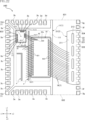
- First embodiment: 1 to 9 show an example of a semiconductor device according to the present disclosure.
- the semiconductor device A10 of this embodiment includes a lead 1, a lead 2, a plurality of leads 3, semiconductor elements 61 and 62, a plurality of wires 7, and a sealing resin 8.
- the semiconductor device A10 is used, for example, in a gate driver circuit of an inverter device such as an electric vehicle or a hybrid vehicle.
- the semiconductor device A10 amplifies a control signal input from the outside and outputs it to a switching element (not shown). Note that the use and function of the semiconductor device A10 are not limited.
- the package format of the semiconductor device A10 is a QFN type. However, the package format of the semiconductor device A10 is not limited to the QFN type.
- FIG. 1 is a perspective view showing the semiconductor device A10.
- FIG. 2 is a plan view showing the semiconductor device A10.
- the outline of the sealing resin 8 is shown by an imaginary line (two-dot chain line) that is transmitted through the sealing resin 8.
- FIG. 3 is a bottom view showing the semiconductor device A10.
- FIG. 4 is a cross-sectional view taken along line IV-IV in FIG. 2.
- FIG. 5 is a sectional view taken along line VV in FIG. 2.
- FIG. 6 is a cross-sectional view taken along line VI-VI in FIG.
- FIG. 7 is a partially enlarged view of FIG. 2.
- FIG. 8 is a partially enlarged view of FIG. 2.
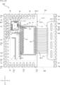
- FIG. 9 is a plan view showing the die pad portion 11 (described later) of the lead 1. As shown in FIG.
- the semiconductor device A10 has a rectangular shape when viewed in the thickness direction (planar view).
- the thickness direction of the semiconductor device A10 is referred to as the thickness direction z
- the direction along one side of the semiconductor device A10 perpendicular to the thickness direction z is referred to as the first direction x
- the direction perpendicular to the thickness direction z and the first direction x is the second direction y.
- the shape and dimensions of the semiconductor device A10 are not limited.
- Lead 1, lead 2, and a plurality of leads 3 are mounted with semiconductor elements 61 and 62 and semiconductor device A10. This is a member that forms a conduction path with the wiring board. Note that some of the plurality of leads 3 include those that are not electrically connected to the semiconductor elements 61 and 62.
- the leads 1 to 3 are formed, for example, by etching or punching a metal plate. Leads 1 to 3 are made of metal, preferably Cu or Ni, or an alloy thereof, 42 alloy, or the like. In this embodiment, the case where leads 1 to 3 are made of Cu will be explained as an example.
- the thickness of the leads 1 to 3 is, for example, 0.08 to 0.3 mm, and in this embodiment is about 0.2 mm.
- the lead 1 is arranged closer to the first side x1 in the first direction x of the semiconductor device A10, and extends throughout the second direction y.
- the lead 2 is spaced apart from the lead 1 and is placed closer to the second side x2 in the first direction x of the semiconductor device A10.
- Each lead 3 is spaced apart from the lead 1 and the lead 2, and spaced apart from each other, and is arranged at either both ends in the first direction x or both ends in the second direction y of the semiconductor device A10.
- lead 1 is larger than lead 2
- each lead 3 is larger than lead 2.
- the lead 1 supports the semiconductor elements 61 and 62 and includes a die pad portion 11 and a plurality of terminal portions 12.
- a semiconductor element 61 and a semiconductor element 62 are mounted on the die pad section 11.
- the die pad portion 11 is located near the first side x1 in the first direction x of the semiconductor device A10, at the center in the second direction y, and has a rectangular shape (or substantially rectangular shape) when viewed in the thickness direction z.
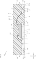
- the die pad portion 11 includes a main surface 111 , a back surface 112 , and a back-side recess 113 .
- the main surface 111 and the back surface 112 face opposite sides in the thickness direction z.
- the main surface 111 faces the first side z1 in the thickness direction z.
- the main surface 111 is a surface on which the semiconductor elements 61 and 62 are mounted.
- the main surface 111 has an edge 111a, as shown in FIG.
- the edge 111a is an edge extending in the second direction y on the first side x1 of the main surface 111 in the first direction x.
- the back surface 112 faces the second side z2 in the thickness direction z. The back surface 112 is exposed from the sealing resin 8 and becomes a back terminal.
- the back side recess 113 is a part where a part of the die pad part 11 is recessed from the back surface 112 toward the first side z1 in the thickness direction z.
- the thickness of the portion of the die pad portion 11 where the back side recess 113 is located is approximately half the thickness of the portion where the back surface 112 is located.
- the back side recess 113 is formed, for example, by half-etching from the second side z2 in the thickness direction z. As shown in FIG. 3, the back surface side recess 113 is arranged around the back surface 112. The back side recess 113 is not exposed from the sealing resin 8 and is covered with the sealing resin 8.
- the shape of the die pad portion 11 is not limited.
- the die pad portion 11 does not need to include the back side recess 113.
- the die pad section 11 includes an opening 4.
- the opening 4 is provided with relatively fine hatching.
- the opening 4 is an opening having an open end on the main surface 111, and in this embodiment, is a recess recessed from the main surface 111 toward the second side z2 in the thickness direction z.
- the depth of the opening 4 (dimension in the thickness direction z) is approximately half the thickness of the die pad portion 11 (the distance between the main surface 111 and the back surface 112 in the thickness direction z).
- the opening 4 is formed, for example, by half etching from the first side z1 in the thickness direction z.
- the opening 4 includes openings 41 to 45, as shown in FIG.
- the opening 41 is located in the first direction x between the semiconductor element 62 and the edge 111a shown by an imaginary line (two-dot chain line) in FIG. 9, and extends in the second direction y.
- both ends of the opening 41 in the second direction y are located inside the outer edge of the main surface 111 when viewed in the thickness direction z.
- the opening 42 is connected to the end of the first side y1 in the second direction y of the opening 41 and extends to the first side x1 in the first direction x. That is, the opening 42 is located on the first side x1 of the opening 41 in the first direction x.
- both ends of the opening 42 in the first direction x are located inside the outer edge of the main surface 111 when viewed in the thickness direction z.
- the semiconductor element 61 shown by an imaginary line (two-dot chain line) in FIG. 9 is arranged on the first side y1 of the opening 42 in the second direction y.
- a portion of the opening 4 that is constituted by the opening 41 and the opening 42 is L-shaped when viewed in the thickness direction z.
- the opening 43 is located between the semiconductor element 62 and the opening 41 in the first direction x, and extends in the second direction y. In this embodiment, both ends of the opening 43 in the second direction y are located inside the outer edge of the main surface 111 when viewed in the thickness direction z.
- the opening 44 is connected to the end of the first side y1 in the second direction y of the opening 43 and extends to the first side x1 in the first direction x. That is, the opening 44 is located on the first side x1 of the opening 43 in the first direction x. Furthermore, the opening 44 is located between the semiconductor element 61 and the opening 42 in the second direction y.
- both ends of the opening 44 in the first direction x are located inside the outer edge of the main surface 111 when viewed in the thickness direction z.
- the opening 45 is connected to the end of the first side y1 in the second direction y of the opening 43 and extends to the first side y1 in the second direction y. That is, the opening 45 is located on the first side y1 of the opening 43 in the second direction y.
- both ends of the opening 45 in the second direction y are located inside the outer edge of the main surface 111 when viewed in the thickness direction z.
- a portion of the opening 4 that is constituted by the opening 43, the opening 44, and the opening 45 is T-shaped when viewed in the thickness direction z.
- the main surface 111 of the die pad section 11 includes a first region 51, a second region 52, and a third region 53, as shown in FIG.
- the first region 51, the second region 52, and the third region 53 are shown by imaginary lines (two-dot chain lines), and are relatively roughly hatched.
- the first region 51 is a region sandwiched between the openings 41 and 42 and the openings 43 and 44.
- the first region 51 is located on the first side x1 of the semiconductor element 62 in the first direction x, and is a region to which the wire 7 (wire 73 described later) is bonded, as shown in FIG.
- the first region 51 may be subjected to plating treatment.
- the plating layer formed by the plating process is made of a metal containing Ag, for example.
- the plating layer protects the lead 1 from impact during wire bonding of the wire 73 while increasing the bonding strength of the wire 73.
- the second region 52 is a region on the second side x2 of the openings 43 and 45 in the first direction x.
- the second region 52 is a region where a semiconductor element 62 is mounted, as shown in FIG.
- the third region 53 is a region on the first side x1 of the opening 45 in the first direction x, and is a region on the first side y1 of the opening 44 in the second direction y.
- the third region 53 is located on the first side x1 from the center of the main surface 111 of the die pad portion 11 in the first direction x, and is located on the first side y1 from the center in the second direction y.
- the third area 53 is an area where the semiconductor element 61 is mounted, as shown in FIG.
- the first region 51, the second region 52, and the third region 53 are regions partitioned by the opening 4.
- the opening 43 partitions a first region 51 and a second region 52.
- the opening 44 partitions the first region 51 and the third region 53.
- the opening 45 partitions a second region 52 and a third region 53. Note that the shape and arrangement of the opening 4 are not limited to those described above, and the shapes and arrangement of the first region 51, second region 52, and third region 53 are not limited to those described above.
- the plurality of terminal parts 12 are joined to the wiring board when the semiconductor device A10 is mounted on the wiring board.
- Each terminal portion 12 is connected to the die pad portion 11 and has a rectangular shape (or approximately rectangular shape) when viewed in the thickness direction z.
- the plurality of terminal sections 12 include six terminal sections 12a, two terminal sections 12b, eight terminal sections 12c, and terminal sections 12d and 12e.
- the six terminal parts 12a are connected to the first side x1 of the die pad part 11 in the first direction x, and are arranged along the second direction y near the second side y2 in the second direction y.
- the six terminal portions 12a overlap the opening 4 (opening 41) when viewed in the first direction x.
- the two terminal portions 12b are connected to the first side y1 of the die pad portion 11 in the second direction y, and are arranged along the second direction y near the second side x2 in the first direction x.
- the eight terminal portions 12c are connected to the second side y2 of the die pad portion 11 in the second direction y, and are arranged along the first direction x.
- the terminal portion 12d is connected to a corner of the first side y1 in the second direction y at the first side x1 in the first direction x of the die pad portion 11.
- the terminal portion 12e is connected to a corner of the die pad portion 11 on the first side x1 in the first direction x and on the second side y2 in the second direction y.
- Each terminal portion 12 includes a main surface 121, a back surface 122, and an end surface 123.
- the main surface 121 and the back surface 122 face opposite to each other in the thickness direction z.
- the main surface 121 faces the first side z1 in the thickness direction z.
- the main surface 121 and the main surface 111 of the die pad portion 11 are flush with each other.
- the back surface 122 faces the second side z2 in the thickness direction z.
- the back surface 122 and the back surface 112 of the die pad portion 11 are spaced apart from each other as shown in FIG. 3, and are at the same position in the thickness direction z.
- the end surface 123 is a surface that is perpendicular to the main surface 121 and the back surface 122 and connected to the main surface 121 and the back surface 122.
- the terminal portion 12d and the terminal portion 12e each include two end surfaces 123.
- the end surface 123 is formed by singulation in the cutting process in the manufacturing process.
- the end surface 123 and the back surface 122 are exposed from the sealing resin 8 and connected, and become a terminal (see FIG. 5). Note that the shape, arrangement position, and number of terminal portions 12 are not limited.
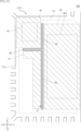
- the lead 2 is spaced apart from the lead 1 on the second side x2 in the first direction x.
- the die pad portion 11 of the lead 1 and the lead 2 are arranged side by side in the first direction x.
- the lead 2 is electrically connected to the semiconductor element 62 by a plurality of wires 7 (a plurality of wires 74 to be described later).
- the lead 2 includes a pad portion 21 and a plurality of terminal portions 22 .
- the pad portion 21 includes a main surface 211, a back surface 212, and a through hole 213.
- the main surface 211 and the back surface 212 face opposite to each other in the thickness direction z.
- the main surface 211 faces the first side z1 in the thickness direction z.
- the main surface 211 is a surface to which the plurality of wires 74 are bonded.
- the main surface 211 includes a bonding region 211a and a non-bonding region 211b.
- the bonded region 211a and the non-bonded region 211b are indicated by imaginary lines (two-dot chain lines).
- the bonding region 211a is a region where the plurality of wires 74 are bonded, and is disposed on the main surface 211 closer to the second side y2 in the second direction y.
- the non-bonded region 211b is a region where the plurality of wires 74 are not bonded, and is arranged on the first side y1 with respect to the bonded region 211a in the second direction y.
- the dimension L1 of the bonding region 211a in the second direction y is 40% or more and 60% or less of the dimension L2 of the lead 2 in the second direction y.
- the bonding region 211a may be subjected to plating treatment.
- the plating layer formed by the plating process is made of a metal containing Ag, for example.
- the plating layer protects the leads 2 from impact during wire bonding of the wires 74 while increasing the bonding strength of the wires 74.
- the back surface 212 faces the second side z2 in the thickness direction z.
- the back surface 212 is covered with the sealing resin 8.
- the thickness of the pad portion 21 (dimension in the thickness direction z) is approximately half the thickness of the die pad portion 11, and is approximately the same as the thickness of the portion of the die pad portion 11 where the backside recess 113 is located.
- the pad portion 21 is formed, for example, by half-etching from the second side z2 in the thickness direction z.
- the through hole 213 is a hole that penetrates the pad portion 21 in the thickness direction z.
- the through hole 213 facilitates filling the back surface 212 side of the pad portion 21 with the material of the sealing resin 8 in the process of forming the sealing resin 8 in the manufacturing process of the semiconductor device A10.
- the pad portion 21 has four rectangular (or substantially rectangular) through holes 213 that are long in the second direction y and are arranged in the second direction y. Note that the shape, number, and arrangement of the through holes 213 are not limited. Further, the pad portion 21 does not need to include the through hole 213.
- the plurality of terminal parts 22 are bonded to the wiring board when the semiconductor device A10 is mounted on the wiring board.
- Each terminal portion 22 is connected to the second side x2 of the pad portion 21 in the first direction x, and has a rectangular shape (or substantially rectangular shape) when viewed in the thickness direction z.
- twelve terminal parts 22 are arranged at equal intervals along the second direction y.
- Each terminal portion 22 includes a main surface 221, a back surface 222, and an end surface 223.
- the main surface 221 and the back surface 222 face opposite to each other in the thickness direction z.
- the main surface 221 faces the first side z1 in the thickness direction z.
- the main surface 221 and the main surface 211 of the pad portion 21 are flush with each other.
- the back surface 222 faces the second side z2 in the thickness direction z.
- the distance L3 between the back surface 222 of the terminal section 22 of the lead 2 and the back surface 112 of the die pad section 11 is sufficiently large, and for example, the distance L3 in the first direction x of the semiconductor device A10 is It is 30% or more and 40% or less.
- the end surface 223 is a surface that is perpendicular to the main surface 221 and the back surface 222 and connected to the main surface 221 and the back surface 222.
- the end surface 223 is formed by singulation in the cutting process in the manufacturing process.
- the end surface 223 and the back surface 222 are exposed from the sealing resin 8 and connected, and become terminals (see FIGS. 4 and 5). Note that the shape, arrangement position, and number of the terminal portions 22 are not limited.
- the plurality of leads 3 constitute a conduction path between the semiconductor elements 61 and 62 and the wiring board on which the semiconductor device A10 is mounted. Note that the plurality of leads 3 also include so-called dummy leads that are not electrically connected to the semiconductor elements 61 and 62. Each lead 3 includes a pad portion 31 and a terminal portion 32.
- the pad portion 31 is a portion to which the wire 7 (wire 71 to be described later) is bonded. Note that the pad portion 31 may or may not be joined to the wire 71.
- the pad portion 31 includes a main surface 311 and a back surface 312.
- the main surface 311 and the back surface 312 face opposite sides in the thickness direction z.
- the main surface 311 faces the first side z1 in the thickness direction z.
- the main surface 311 is a surface to which the wire 71 is bonded.
- the main surface 311 may be subjected to plating treatment.
- the plating layer formed by the plating process is made of a metal containing Ag, for example.
- the plating layer protects the leads 3 from impact during wire bonding of the wires 71 while increasing the bonding strength of the wires 71.
- the plating layer may be formed only on the lead 3 to which the wire 71 is bonded.
- the back surface 312 faces the second side z2 in the thickness direction z.
- the back surface 312 is covered with sealing resin 8.
- the thickness of the pad portion 31 (dimension in the thickness direction z) is approximately half the thickness of the die pad portion 11, and is approximately the same as the thickness of the portion of the die pad portion 11 where the back side recess 113 is located.
- the pad portion 31 is formed, for example, by half-etching from the second side z2 in the thickness direction z.
- the terminal portion 32 is bonded to the wiring board when the semiconductor device A10 is mounted on the wiring board.
- the terminal portion 32 is connected to the pad portion 31 and has a rectangular shape (or a substantially rectangular shape) when viewed in the thickness direction z.
- the terminal portion 32 includes a main surface 321, a back surface 322, and an end surface 323.
- the main surface 321 and the back surface 322 face opposite to each other in the thickness direction z.
- the main surface 321 faces the first side z1 in the thickness direction z.
- the main surface 321 and the main surface 311 of the pad portion 31 are flush with each other.
- the wire 71 may be joined to the main surface 321 of the terminal portion 32.
- the back surface 322 faces the second side z2 in the thickness direction z.
- the end surface 323 is a surface that is perpendicular to the main surface 321 and the back surface 322 and connected to the main surface 321 and the back surface 322.
- the end surface 323 is formed by singulation in the cutting process in the manufacturing process.
- the end surface 323 and the back surface 322 are exposed from the sealing resin 8 and connected, and become a terminal (see FIG. 4). Note that the shape of the terminal portion 32 is not limited.
- the plurality of leads 3 include a plurality of leads 3a, a plurality of leads 3b, a lead 3c, a lead 3e, a pair of leads 3f, and a pair of leads 3g.
- the plurality of leads 3 include seven leads 3a. Note that the number of leads 3a is not limited.
- the plurality of leads 3a are arranged near the first side y1 in the second direction y at the end of the first side x1 in the first direction x of the semiconductor device A10.
- the plurality of leads 3a are arranged on the first side x1 of the die pad portion 11 in the first direction x, and along the second direction y between the terminal portions 12a and 12d in the second direction y.
- the plurality of leads 3 includes seven leads 3b. Note that the number of leads 3b is not limited.
- the plurality of leads 3b are arranged near the first side x1 in the first direction x at the end of the first side y1 in the second direction y of the semiconductor device A10.
- the plurality of leads 3b are arranged on the first side y1 of the die pad portion 11 in the second direction y, between the terminal portions 12b and 12d in the first direction x.
- the plurality of leads 3a and the plurality of leads 3b are arranged so as to be electrically connected to the semiconductor element 61 via the wire 71. In this embodiment, most of the plurality of leads 3a and the plurality of leads 3b are electrically connected to the semiconductor element 61, but some are not electrically connected to the semiconductor element 61.
- each pad portion 31 of the plurality of leads 3a and the plurality of leads 3b extends toward the element center 61c, which is the center of the semiconductor element 61, when viewed in the thickness direction z.
- the plurality of leads 3 include one lead 3c and one lead 3e.
- the number of leads 3c and leads 3e is not limited.
- the lead 3c is arranged on the first side x1 of the die pad section 11 in the first direction x, between the terminal section 12a and the terminal section 12e in the second direction y.
- the lead 3e is arranged on the second side y2 of the die pad section 11 in the second direction y, between the terminal section 12c and the terminal section 12e in the first direction x. Leads 3c and 3e are so-called dummy leads.
- the plurality of leads 3 include a pair of leads 3f and a pair of leads 3g.
- the pair of leads 3g are arranged one each on the first side y1 and the second side y2 of the lead 2 in the second direction y.
- One lead 3g is arranged at a corner of the first side y1 in the second direction y on the second side x2 in the first direction x of the semiconductor device A10, and the other lead 3g is arranged on the second side x2 in the first direction It is arranged at the corner of the second side y2 in the second direction y on the side x2.
- the plurality of leads 3 may not include the lead 3g.
- the pair of leads 3f is arranged one each on the first side y1 and the second side y2 of the lead 2 in the second direction y.
- Each lead 3f is arranged between the lead 2 and each lead 3g in the second direction y. Note that the number of leads 3f is not limited. Lead 3f and lead 3g are so-called dummy leads.
- a plating layer containing Sn may be disposed on the surfaces of the leads 1 to 3 exposed from the sealing resin 8.
- the constituent material of the plating layer is not limited.
- the plating layer ensures good adhesion of solder to the exposed surface and prevents erosion of the exposed portion caused by soldering. do.
- the shape and arrangement of the leads 1 to 3 are not limited to the above.
- the semiconductor element 61 and the semiconductor element 62 are elements that perform the electrical functions of the semiconductor device A10.
- the semiconductor element 62 is a switching element.
- the semiconductor element 62 is a HEMT (High Electron Mobility Transistor) using gallium nitride (GaN).
- the semiconductor element 62 may be made of a nitride semiconductor other than GaN.
- the semiconductor element 62 may be an IGBT (Insulated Gate Bipolar Transistor), a MOSFET (Metal Oxide Semiconductor Field Effect Transistor), a bipolar transistor, or the like.
- the semiconductor element 62 includes an element main surface 62a, an element back surface 62b, a plurality of first electrodes 621, a second electrode 622, and a plurality of third electrodes 623.
- the element main surface 62a and the element back surface 62b face opposite to each other in the thickness direction z.
- the element main surface 62a is a surface facing the first side z1 in the thickness direction z
- the element back surface 62b is a surface facing the second side z2 in the thickness direction z.
- a plurality of first electrodes 621, a plurality of second electrodes 622, and a plurality of third electrodes 623 are arranged on the element main surface 62a.
- the plurality of first electrodes 621 are source electrodes, and are arranged side by side along the second direction y closer to the first side x1 in the first direction x of the element main surface 62a.
- the second electrode 622 is a gate electrode, and is arranged near the first side y1 in the second direction y of the element main surface 62a.
- the plurality of third electrodes 623 are drain electrodes, and are arranged side by side along the second direction y closer to the second side x2 of the first direction x of the element main surface 62a. Note that other electrodes are also arranged on the element main surface 62a. Furthermore, the layout of the electrodes 621 to 623 is not limited.
- the back surface 62b of the semiconductor element 62 is bonded to the main surface 111 of the die pad portion 11 via a bonding member 65.
- the bonding member 65 is, for example, Ag paste.
- the bonding member 65 may be a conductive bonding material such as solder or a sintered silver bonding material, or may be an insulating bonding member.
- the semiconductor element 62 is disposed on the second region 52 of the main surface 111, that is, on the second side x2 of the openings 43 and 44 in the first direction x.
- the semiconductor element 61 is a driving element that drives the semiconductor element 62.
- the semiconductor element 61 generates a drive signal based on a control signal input from the outside and outputs it to the semiconductor element 62. Further, the semiconductor element 61 controls the drive signal based on a source sense signal inputted from the semiconductor element 62 and the like.
- the semiconductor element 61 includes an element main surface 61a, an element back surface 61b, and a plurality of electrodes 611.
- the element main surface 61a and the element back surface 61b face opposite sides in the thickness direction z.
- the element main surface 61a is a surface facing the first side z1 in the thickness direction z
- the element back surface 61b is a surface facing the second side z2 in the thickness direction z.
- the plurality of electrodes 611 are arranged on the element main surface 61a. Note that the function and arrangement of each electrode 611 are not limited.
- the semiconductor element 61 has its back surface 61b bonded to the main surface 111 of the die pad portion 11 via a bonding member 65.
- the semiconductor element 61 is located on the third region 53 of the main surface 111, that is, on the first side x1 of the opening 45 in the first direction x, and on the second side of the opening 44. It is arranged on the first side y1 in the direction y.
- the semiconductor element 61 is arranged on a first side x1 with respect to the semiconductor element 62 in the first direction x, and on a first side y1 with respect to the semiconductor element 62 in the second direction y.
- the element center 61c which is the center of the semiconductor element 61 as viewed in the thickness direction z, is located on the first side y1 from the center of the main surface 111 of the die pad portion 11 in the second direction y, and It is located on the first side x1 from the center in the direction x.
- each wire 7 includes a plurality of wires 71, 72, 73, and 74.
- the plurality of wires 71 constitute a conduction path between the semiconductor element 61 and the plurality of leads 3, as shown in FIGS. 2 and 8.
- Each wire 71 is electrically connected to one of the electrodes 611 of the semiconductor element 61 and the main surface 311 of one of the pad portions 31 of the plurality of leads 3a or the plurality of leads 3b.
- the semiconductor element 61 can receive signals from the outside via the plurality of leads 3 and wires 71, and can also output signals to the outside.
- each wire 71 is connected to the It can be formed on other leads 3 adjacent to one lead 3 so as not to overlap when viewed in the thickness direction z.
- the plurality of wires 72 constitute a conduction path between the semiconductor element 61 and the semiconductor element 62, as shown in FIGS. 2 and 8.
- One wire 72 is electrically connected to one of the electrodes 611 of the semiconductor element 61 and the second electrode 622 of the semiconductor element 62 .
- the semiconductor element 61 outputs a drive signal to the second electrode 622 via the wire 72 .
- the other wires 72 are electrically connected to one of the electrodes 611 of the semiconductor element 61 and one of the electrodes of the semiconductor element 62.
- a source sense signal is input to the semiconductor element 61 via a wire 72 connected to a first electrode 621 (source electrode) of the semiconductor element 62 . Further, the semiconductor element 61 inputs and outputs signals to and from the semiconductor element 62 via another wire 72 .
- the plurality of wires 73 constitute a conduction path between the semiconductor element 62 and the die pad portion 11, as shown in FIGS. 2 and 8.
- Each wire 73 is electrically connected to one of the first electrodes 621 of the semiconductor element 62 and the main surface 111 of the die pad section 11 .
- the lead 1 is electrically connected to the first electrode 621 (source electrode) of the semiconductor element 62 and functions as a source terminal.
- each wire 73 is joined to the first region 51 of the main surface 111.
- the plurality of wires 74 constitute a conduction path between the semiconductor element 62 and the lead 2, as shown in FIGS. 2 and 7.
- Each wire 74 is electrically connected to one of the third electrodes 623 of the semiconductor element 62 and the main surface 211 of the pad portion 21 of the lead 2 .
- the lead 2 is electrically connected to the third electrode 623 (drain electrode) of the semiconductor element 62 and functions as a drain terminal.
- each wire 74 is joined to the joining region 211a of the main surface 211. All of the wires 74 are inclined with respect to the first direction x when viewed in the thickness direction z. As shown in FIG.
- each wire 74 includes a bonding portion 74a bonded to the semiconductor element 62 and a bonding portion 74b bonded to the lead 2. As shown in FIG. The joint portion 74a is located on the first side y1 in the second direction y from the joint portion 74b.
- each wire 74 is curved toward the second side y2 in the second direction y. Moreover, since each wire 74 is inclined with respect to the first direction x when viewed in the thickness direction z, the force applied to the wire 74 by the material of the sealing resin 8 is perpendicular to the component in the direction parallel to the wire 74.
- the sealing resin 8 covers a portion of each of the leads 1 to 3, the semiconductor elements 61 and 62, and the plurality of wires 7.
- the sealing resin 8 has electrical insulation properties.
- the sealing resin 8 is made of a material containing, for example, a black epoxy resin. Note that the material of the sealing resin 8 is not limited.
- the sealing resin 8 includes a resin main surface 81, a resin back surface 82, and four resin side surfaces 83.
- the main resin surface 81 and the resin back surface 82 face opposite sides in the thickness direction z.
- the main resin surface 81 is a surface facing the first side z1 in the thickness direction z
- the resin back surface 82 is a surface facing the second side z2 in the thickness direction z.
- the four resin side surfaces 83 are surfaces that are perpendicular to the resin main surface 81 and the resin back surface 82, connect the resin main surface 81 and the resin back surface 82, and face outward in the first direction x or the second direction y. It is. Each resin side surface 83 is formed by singulation in the cutting process in the manufacturing process.
- the four resin side surfaces 83 include a first resin side surface 831 , a second resin side surface 832 , a third resin side surface 833 , and a fourth resin side surface 834 .
- the first resin side surface 831 and the second resin side surface 832 face opposite to each other in the second direction y.
- the first resin side surface 831 is a surface disposed on the first side y1 in the second direction y and faces the first side y1
- the second resin side surface 832 is a surface disposed on the second side y2 in the second direction y. This is the surface facing the second side y2.
- the third resin side surface 833 and the fourth resin side surface 834 face opposite to each other in the first direction x.
- the third resin side surface 833 is a surface disposed on the first side x1 in the first direction x and faces the first side x1
- the fourth resin side surface 834 is a surface disposed on the second side x2 in the first direction x. This is the surface facing the second side x2.
- Each end surface 123 of the lead 1 facing the first side x1 in the first direction x and the end surface 323 of each lead 3a and lead 3c are exposed from the third resin side surface 833 and are flush with the third resin side surface 833. be.
- Each end surface 123 and each end surface 323 exposed from the third resin side surface 833 are spaced apart from each other and arranged at equal intervals along the second direction y.
- Each end surface 123 of the lead 1 facing the first side y1 in the second direction y, the end surface 323 of each lead 3b, and the end surface 323 of the lead 3g facing the first side y1 are exposed from the first resin side surface 831, It is flush with the first resin side surface 831.
- Each end surface 123 exposed from the first resin side surface 831 and the end surface 323 of each lead 3b are spaced apart from each other and arranged at equal intervals along the first direction x.
- Each end surface 123 of the lead 1 facing the second side y2 in the second direction y, the end surface 323 of the lead 3e, and the end surface 323 of the lead 3g facing the second side y2 are exposed from the second resin side surface 832 and It is flush with the two resin side surfaces 832.
- Each end surface 123 exposed from the second resin side surface 832 and the end surface 323 of each lead 3e are spaced apart from each other and arranged at equal intervals along the first direction x.
- each terminal portion 22 of the lead 2, the end surface 323 of each lead 3f, and the end surface 323 of each lead 3g facing the second side x2 are exposed from the fourth resin side surface 834 and are connected to the fourth resin side surface 834. They are on the same level as each other. Each end surface 223 and each end surface 323 exposed from the fourth resin side surface 834 are spaced apart from each other and arranged at equal intervals along the second direction y. Further, the back surface 112 of the die pad section 11 of the lead 1 and the back surface 122 of each terminal section 12, the back surface 222 of each terminal section 22 of the lead 2, and the back surface 322 of the terminal section 32 of each lead 3 are separated from the resin back surface 82. It is exposed and flush with the resin back surface 82.
- the semiconductor element 61 is mounted at a position shifted toward the first side y1 from the center of the main surface 111 of the die pad portion 11 in the second direction y. Further, the pad portion 31 of each lead 3a extends toward the element center 61c when viewed in the thickness direction z. Therefore, the wire 71 bonded to each lead 3a can be formed so as not to overlap other leads 3a adjacent to the lead 3a to which the wire 71 is bonded when viewed in the thickness direction z. Thereby, the semiconductor device A10 can suppress each wire 71 from coming into contact with the other adjacent lead 3a.
- the semiconductor element 61 is mounted at a position shifted toward the first side x1 from the center of the main surface 111 of the die pad portion 11 in the first direction x. Further, the pad portion 31 of each lead 3b extends toward the element center 61c when viewed in the thickness direction z. Therefore, the wire 71 bonded to each lead 3b can be formed so as not to overlap other leads 3b adjacent to the lead 3b to which the wire 71 is bonded when viewed in the thickness direction z. Thereby, the semiconductor device A10 can suppress each wire 71 from coming into contact with the other adjacent lead 3b.
- each wire 74 is inclined with respect to the first direction x when viewed in the thickness direction z. Therefore, compared to the case where the wires 74 are parallel to the first direction x, the material of the sealing resin 8 flowing in the second direction y is The force exerted on becomes smaller. This suppresses the wire flow of each wire 74, so that in the semiconductor device A10, contact between the wires 74 due to the wire flow is suppressed.
- the bonding portion 74a of each wire 74 is located on the first side y1 in the second direction y from the bonding portion 74b, and the inclination direction with respect to the first direction x is the same. Therefore, since the wire flow that occurs in each wire 74 is the same, in the semiconductor device A10, contact between the wires 74 due to wire flow is suppressed.
- the die pad portion 11 includes the opening 4, which is a recessed portion recessed from the main surface 111 toward the second side z2 in the thickness direction z.
- the opening 4 includes an opening 41 located between the first region 51 to which the wire 73 is bonded and the edge 111a in the first direction x, and extending in the second direction y.
- the opening 41 prevents the peeling generated at the edge 111a from progressing toward the second side x2 in the first direction x. Since the opening 41 prevents the separation from progressing to the first region 51, the semiconductor device A10 can suppress the separation of the wire 73 from the die pad portion 11.
- the opening 4 includes an opening 42 that is connected to the end of the first side y1 in the second direction y of the opening 41 and extends to the first side x1 in the first direction x. .
- the opening 42 prevents the peeling generated at the edge 111a from progressing toward the first side y1 in the second direction y. Since the opening 42 prevents the peeling from progressing to the first region 51 and the second region 52, the semiconductor device A10 prevents the peeling of the wire 73 from the die pad portion 11 and the peeling of the semiconductor element 61 from the die pad portion 11. It can be suppressed.
- the opening 4 is located between the second region 52 where the semiconductor element 62 is mounted and the first region 51 where the wire 73 is bonded in the first direction x, and , and includes an opening 43 extending in the second direction y.
- the opening 43 can suppress the melted bonding member 65 from flowing to the first region 51. This can prevent the joining member 65 from interfering with joining the wires 73.
- the opening 43 prevents the peeling of the sealing resin 8 from the die pad portion 11 from progressing toward the first side x1 in the first direction x, it can also contribute to suppressing the peeling of the wire 73 from the die pad portion 11.
- the opening 4 includes an opening 44 that is connected to the end of the first side y1 in the second direction y of the opening 43 and extends to the first side x1 in the first direction x. . In the manufacturing process, even if the molten bonding member 65 flows out when the semiconductor element 61 is bonded to the die pad portion 11, the opening 44 can prevent the molten bonding member 65 from flowing to the first region 51. This can prevent the joining member 65 from interfering with joining the wires 73.
- the opening 44 prevents the peeling of the sealing resin 8 from the die pad portion 11 from progressing toward the second side y2 in the second direction y, it can also contribute to suppressing the peeling of the wire 73 from the die pad portion 11.
- the opening 4 includes an opening 45 that is connected to the end of the first side y1 in the second direction y of the opening 43 and extends to the first side y1 in the second direction y. .
- the opening 45 suppresses the concentration of stress at the connection point between the opening 43 and the opening 44, and further strengthens the bond between the sealing resin 8 and the die pad portion 11.
- the opening 43, the opening 44, and the opening 45 partition the first region 51, the second region 52, and the third region 53, and determine the positions for mounting the semiconductor element 61 and the semiconductor element 62. It also has the function of clarifying.
- each end of the opening 4 is located inside the outer edge of the main surface 111 of the die pad section 11. Therefore, the strength of the die pad portion 11 can be increased compared to the case where each end portion extends to the outer edge of the main surface 111.
- the opening 4 is a recessed portion recessed from the main surface 111 toward the second side z2 in the thickness direction z. Therefore, the strength of the die pad portion 11 can be increased compared to the case where the opening portion 4 penetrates the die pad portion 11 in the thickness direction z.
- the distance between the back surface 112 of the die pad section 11 and the back surface 222 of the terminal section 22 of the lead 2 is sufficiently large. Therefore, conduction between the back surface 112 and the back surface 222 due to dielectric breakdown is suppressed.
- the dimension of the pad portion 21 of the lead 2 in the first direction x is sufficiently large. Thereby, the length of the wire 74 that electrically connects the semiconductor element 62 and the pad portion 21 can be suppressed.
- the semiconductor device A10 includes leads 3c, 3e, 3f, and 3g that are dummy leads. Therefore, the semiconductor device A10 has improved mounting reliability compared to the case where the leads 3c, 3e, 3f, and 3g are not provided.
- the lead 1 includes terminal portions 12a, 12b, and 12c. Therefore, in the semiconductor device A10, heat dissipation is enhanced and the strength supporting the die pad section 11 is improved, compared to the case where the terminal sections 12a, 12b, and 12c are replaced by leads spaced apart from the leads 1. There is.
- each wire 74 is inclined with respect to the first direction x when viewed in the thickness direction z, but the present invention is not limited to this.
- Each wire 74 may be parallel to the first direction x when viewed in the thickness direction z.
- each lead 3a and each lead 3b extend toward the element center 61c when viewed in the thickness direction z, but the present invention is not limited to this.
- the pad portion 31 of each lead 3a may extend to the second side x2 in the first direction x.
- the pad portion 31 of each lead 3b may extend to the second side y2 in the second direction y.
- the package format of the semiconductor device A10, the type and number of the semiconductor elements 61 and 62 mounted, the shape, number, and arrangement of the leads 1 to 3 are not particularly limited.
- the bonding region 211a is arranged closer to the second side y2 in the second direction y of the main surface 211, but the present invention is not limited to this.
- the bonding region 211a may be arranged closer to the first side y1 of the main surface 211 in the second direction y.
- the joint portion 74a of the wire 74 is located on the second side y2 in the second direction y from the joint portion 74b.
- FIG. 10 is a diagram for explaining a semiconductor device A11 according to a first modification of the first embodiment.
- FIG. 10 is a plan view showing the die pad section 11 of the semiconductor device A11, and corresponds to FIG.
- the semiconductor device A11 is different from the semiconductor device A10 in the configuration of the opening 4.
- the opening 4 of the semiconductor device A11 according to this modification does not include the opening 42 and the opening 45. Also in this modification, since the opening 4 includes the opening 41, the peeling generated at the edge 111a is prevented from progressing to the first region 51, and the peeling of the wire 73 from the die pad portion 11 is suppressed. Ru. Further, since the opening 4 includes the opening 43 and the opening 44, it is possible to suppress the melted bonding member 65 from flowing into the first region 51, and also to suppress the wire 73 from peeling off from the die pad section 11. can also contribute.
- FIG. 11 is a diagram for explaining a semiconductor device A12 according to a second modification of the first embodiment.
- FIG. 11 is a plan view showing the die pad section 11 of the semiconductor device A12, and corresponds to FIG. 9. As shown in FIG. The semiconductor device A12 differs from the semiconductor device A10 in the configuration of the opening 4.
- the opening 4 of the semiconductor device A12 according to this modification does not include the openings 43 to 45. Also in this modification, since the opening 4 includes the openings 41 and 42, the progress of peeling to the first region 51 and the second region 52 is prevented, and the separation from the wire 73 and the die pad portion 11 of the semiconductor element 61 is prevented. Peeling is suppressed.
- FIG. 12 is a diagram for explaining a semiconductor device A13 according to a third modification of the first embodiment.
- FIG. 12 is a plan view showing the die pad section 11 of the semiconductor device A13, and corresponds to FIG.
- the semiconductor device A13 is different from the semiconductor device A10 in the configuration of the opening 4.
- the opening 4 of the semiconductor device A13 according to this modification does not include the openings 41 and 42. Also in this modification, since the opening 4 includes the openings 43 and 44, it is possible to suppress the melted bonding member 65 from flowing out to the first region 51, and to prevent the wire 73 from peeling off from the die pad portion 11. It can also contribute to suppression. Furthermore, since the opening 4 includes the opening 45, concentration of stress at the connection point between the opening 43 and the opening 44 is suppressed, and the bonding between the sealing resin 8 and the die pad portion 11 is made stronger. become.
- the main surface 111 of the die pad section 11 is divided into a first region 51, a second region 52, and a third region 53 by the openings 43 to 45, the positions for mounting the semiconductor element 61 and the semiconductor element 62 are determined. becomes clear.
- the opening 4 does not need to include all of the openings 41 to 45.
- the opening 4 only needs to include necessary portions of the openings 41 to 45.
- FIG. 13 is a diagram for explaining a semiconductor device A14 according to a fourth modification of the first embodiment.
- FIG. 13 is a plan view showing the die pad section 11 of the semiconductor device A14, and corresponds to FIG. 9.
- the semiconductor device A14 is different from the semiconductor device A10 in the configuration of the opening 4.
- the opening 41 and the opening 42 are not connected and are spaced apart from each other, and the opening 43, the opening 44, and the opening 45 are not connected and are separated from each other. They are separated. Even if the openings 41 to 45 are not connected to each other and are spaced apart, each of them can prevent the progress of peeling and can also prevent the flow of the molten bonding member 65. It should be noted that since there is a risk that peeling may progress through the separated portions or that the molten joining member 65 may flow out from the separated portions, it is desirable that the distance between the separated portions be small, and it is better that the separated portions are connected. desirable.
- FIG. 14 is a diagram for explaining a semiconductor device A15 according to a fifth modification of the first embodiment.
- FIG. 14 is a plan view showing the die pad section 11 of the semiconductor device A15, and corresponds to FIG.
- the semiconductor device A15 is different from the semiconductor device A10 in the configuration of the opening 4.
- the openings 4 of the semiconductor device A15 are arranged in the first direction x or the second direction y instead of having the openings 41 to 45 extending in the first direction x or the second direction y, respectively. It consists of a plurality of parts 4a.
- Each portion 4a has, for example, a rectangular shape when viewed in the thickness direction z, and is a recessed portion recessed from the main surface 111 toward the second side z2 in the thickness direction z. Note that the shape and size of each portion 4a viewed in the thickness direction z are not limited.
- the openings 41 to 45 each perform the same functions as the openings 41 to 45 of the semiconductor device A10.
- FIG. 15 is a diagram for explaining a semiconductor device A16 according to a sixth modification of the first embodiment.
- FIG. 15 is a plan view showing the die pad section 11 of the semiconductor device A16, and corresponds to FIG.
- the semiconductor device A16 is different from the semiconductor device A10 in the configuration of the opening 4.
- the opening 4 of the semiconductor device A13 does not have a shape in which each of the openings 41 to 45 extends in the first direction x or the second direction y, but is an aggregate of a plurality of portions 4b.
- Each portion 4b has, for example, a circular shape when viewed in the thickness direction z, and is a recessed portion recessed from the main surface 111 toward the second side z2 in the thickness direction z. Note that the shape and size of each portion 4a viewed in the thickness direction z are not limited.
- the openings 41 to 45 each perform the same functions as the openings 41 to 45 of the semiconductor device A10.
- FIG. 16 is a diagram for explaining a semiconductor device A17 according to a seventh modification of the first embodiment.
- FIG. 16 is a plan view showing the die pad section 11 of the semiconductor device A17, and corresponds to FIG. 9.
- the semiconductor device A17 is different from the semiconductor device A10 in the configuration of the opening 4.
- the opening 41 of the semiconductor device A13 according to this modification has an end on the second side y2 in the second direction y reaching the outer edge of the main surface 111.
- the end of the second side y2 of the opening 43 in the second direction y, the end of the first side x1 of the opening 42 in the first direction x, and the first side x1 of the opening 44 in the first direction x. and the end of the opening 45 on the first side y1 in the second direction y also reach the outer edge of the main surface 111.
- the openings 41 to 45 each perform the same functions as the openings 41 to 45 of the semiconductor device A10.
- FIG. 17 is a diagram for explaining a semiconductor device A18 according to an eighth modification of the first embodiment.
- FIG. 17 is a plan view showing the die pad section 11 of the semiconductor device A18, and corresponds to FIG.
- the semiconductor device A18 is different from the semiconductor device A10 in the configuration of the opening 4.
- the opening 4 of the semiconductor device A18 further includes an opening 46 and an opening 47.
- the opening 46 is connected to an end of the second side y2 in the second direction y of the opening 41 and an end of the second side y2 of the opening 43 in the second direction y, and extends in the first direction x.
- the opening 47 is connected to an end of the opening 42 on the first side x1 in the first direction x and an end of the opening 44 on the first side x1 in the first direction x, and extends in the second direction y.
- the opening 46 prevents the peeling from progressing in the second direction y toward the first side y1 and prevents the peeling from progressing toward the first region 51.
- the opening 47 prevents the peeling from progressing in the first direction x toward the second side x2, and prevents the peeling from progressing toward the first region 51. Therefore, in the semiconductor device A18, separation of the wire 73 from the die pad portion 11 can be further suppressed.
- FIG. 18 is a diagram for explaining a semiconductor device A19 according to a ninth modification of the first embodiment.
- FIG. 18 is a plan view showing the die pad section 11 of the semiconductor device A19, and corresponds to FIG.
- the semiconductor device A19 is different from the semiconductor device A10 in the configuration of the opening 4.
- the opening 41 of the semiconductor device A19 according to this modification is arranged at the same position in the first direction x as the end of the opening 44 on the first side x1 in the first direction x.
- the opening 41 may be connected to the opening 44.
- the opening 42 is connected to the end of the second side y2 in the second direction y of the opening 41, and extends to the second side x2 in the first direction x.
- the opening 42 may be connected to the opening 43.
- the opening 41 performs the same function as the opening 41 of the semiconductor device A10.
- the opening 42 prevents the delamination from progressing toward the first side y1 in the second direction y, and prevents the delamination from progressing toward the first region 51. Therefore, in the semiconductor device A19, separation of the wire 73 from the die pad portion 11 can be further suppressed.
- FIG. 19 is a diagram for explaining a semiconductor device A20 according to a second embodiment of the present disclosure.
- FIG. 19 is a cross-sectional view showing the semiconductor device A20, and corresponds to FIG. 5.
- the semiconductor device A20 of this embodiment differs from the first embodiment in that the opening 4 penetrates the die pad portion 11 in the thickness direction z.
- the configuration and operation of other parts of this embodiment are similar to those of the first embodiment. Note that each part of the first embodiment and each modification example described above may be combined arbitrarily. In this embodiment, all of the openings 41 to 45 of the opening 4 penetrate the die pad portion 11 in the thickness direction z.
- the openings 41 to 45 each prevent the progress of peeling and also prevent the melted bonding member 65 from flowing out, so they perform the same functions as the openings 41 to 45 of the semiconductor device A10.
- the semiconductor device A20 can suppress separation of the wire 73 from the die pad portion 11, and can also suppress the bonding member 65 from interfering with the bonding of the wire 73.
- the semiconductor device A20 has the same configuration as the semiconductor device A10, and thus achieves the same effects as the semiconductor device A10.
- FIG. 20 is a diagram for explaining a semiconductor device A30 according to a third embodiment of the present disclosure.
- FIG. 20 is a plan view showing the semiconductor device A30, and corresponds to FIG. 2.
- the outer shape of the sealing resin 8 is shown by an imaginary line (two-dot chain line) that is transmitted through the sealing resin 8.
- the shape of the lead 2 is different from that of the first embodiment.
- the configuration and operation of other parts of this embodiment are similar to those of the first embodiment. Note that each part of the first to second embodiments and each modification example described above may be combined arbitrarily.
- the lead 2 according to the present embodiment has a larger dimension in the second direction y than the lead 2 according to the first embodiment, and includes 14 terminal parts 22.
- the semiconductor device A30 does not include the lead 3f, and the pad portion 21 extends in the second direction y to the position where the lead 3f was arranged in the first embodiment.
- the lead 2 according to this embodiment is the lead 3f in the first embodiment connected to the lead 2.
- the plurality of wires 74 are joined to the second side y2 of the main surface 211 of the pad section 21 in the second direction y. There is.
- each wire 74 is inclined with respect to the first direction x when viewed in the thickness direction z, the wire flow of each wire 74 is suppressed, and the semiconductor device A30 is Contact between the wires 74 due to this is suppressed. Also in this embodiment, since each wire 74 has the same inclination direction with respect to the first direction Contact is suppressed. Further, according to the present embodiment, since the bonding portion 74b of each wire 74 is bonded to the second side y2 of the main surface 211 of the pad portion 21 in the second direction y, the bonding portion 74b of each wire 74 The inclination angle ⁇ with respect to the first embodiment is larger than that in the first embodiment. This reduces the component that affects the wire flow, so that the wire flow is further suppressed in the semiconductor device A30. Further, the semiconductor device A30 has the same configuration as the semiconductor device A10, and thus achieves the same effects as the semiconductor device A10.
- FIG. 21 is a diagram for explaining a semiconductor device A31 according to a first modification of the third embodiment.
- FIG. 21 is a plan view showing the semiconductor device A31, and corresponds to FIG. 2.
- the outer shape of the sealing resin 8 is shown by an imaginary line (two-dot chain line) that is transmitted through the sealing resin 8.
- the same or similar elements as in the third embodiment are given the same reference numerals as in the third embodiment, and redundant explanation will be omitted.
- the semiconductor device A31 is different from the semiconductor device A30 in the shape of the leads 2.
- the lead 2 of the semiconductor device A31 according to this modification has a larger dimension in the second direction y than the lead 2 according to the third embodiment, and includes 16 terminal portions 22.
- the semiconductor device A31 does not include the lead 3g, and the pad portion 21 extends in the second direction y to the position where the lead 3g was arranged in the third embodiment. That is, in the lead 2 according to this modification, the lead 3g in the third embodiment is connected to the lead 2.
- the dimension of the pad section 21 in the second direction y is further increased, so that the plurality of wires 74 are bonded to the second side y2 of the main surface 211 of the pad section 21 in the second direction y. ing.
- the inclination angle ⁇ of each wire 74 with respect to the first direction x is larger than that in the third embodiment. This reduces the component that affects the wire flow, so that the wire flow is further suppressed in the semiconductor device A31.
- FIG. 22 is a diagram for explaining a semiconductor device A40 according to a fourth embodiment of the present disclosure.
- FIG. 22 is a plan view showing the semiconductor device A40, and corresponds to FIG. 2.
- the outer shape of the sealing resin 8 is shown by an imaginary line (two-dot chain line) that is transmitted through the sealing resin 8.
- the semiconductor device A40 of this embodiment is different from the first embodiment in the structure of the lead 1.
- the configuration and operation of other parts of this embodiment are similar to those of the first embodiment. Note that each part of the first to third embodiments and each modification example described above may be combined arbitrarily.
- the lead 1 does not include the terminal portion 12a, the terminal portion 12b, and the terminal portion 12c.
- the semiconductor device A40 includes a lead 3c in place of the terminal portion 12a, a lead 3d in place of the terminal portion 12b, and a lead 3e in place of the terminal portion 12c.
- the leads 3c, 3d, and 3e have the same configuration as the other leads 3, and are spaced apart from the die pad portion 11.
- Each lead 3c is arranged on the second side y2 with respect to the plurality of leads 3a in the second direction y. In each lead 3c, the pad portion 31 extends to the second side x2 in the first direction x.
- Each lead 3d is arranged on the second side x2 with respect to the plurality of leads 3b in the first direction x.
- the pad portion 31 extends to the second side y2 in the second direction y.
- Each lead 3e is arranged on the second side x2 with respect to the terminal portion 12e in the first direction x. In each lead 3e, the pad portion 31 extends to the first side y1 in the second direction y.
- Leads 3c, 3d, and 3e are so-called dummy leads.
- the semiconductor device A40 has the same configuration as the semiconductor device A10, and thus achieves the same effects as the semiconductor device A10.
- FIG. 23 is a diagram for explaining a semiconductor device A50 according to a fifth embodiment of the present disclosure.
- FIG. 23 is a plan view showing the semiconductor device A50, and corresponds to FIG. 2.
- the outer shape of the sealing resin 8 is shown by an imaginary line (two-dot chain line) that is transmitted through the sealing resin 8.
- the semiconductor device A50 of this embodiment differs from the first embodiment in that the plurality of wires 74 are all parallel (or substantially parallel) to the first direction x when viewed in the thickness direction z.
- the configuration and operation of other parts of this embodiment are similar to those of the first embodiment. Note that each part of the above-described first to fourth embodiments and each modification may be arbitrarily combined.
- the bonding portion 74a bonded to the semiconductor element 62 and the bonding portion 74b bonded to the lead 2 are at the same position in the second direction y. That is, all of the plurality of wires 74 are parallel (or substantially parallel) to the first direction x when viewed in the thickness direction z.
- each wire 74 is parallel (or substantially parallel) to the first direction x when viewed in the thickness direction z, so compared to the case where it is inclined with respect to the first direction x, Wire length can be shortened.
- the semiconductor device A50 can suppress the resistance value of the wire 74.
- the semiconductor device A50 has the same configuration as the semiconductor device A10, and thus achieves the same effects as the semiconductor device A10.
- the semiconductor element 61 is located on the first side x1 in the first direction x and the first side y1 in the second direction y with respect to the semiconductor element 62, and the semiconductor element 61 is located on the first side y1 in the second direction y.
- the main surface 111 is disposed at a position shifted from the center of the main surface 111 on the first side x1 in the first direction x to the first side y1 in the second direction y
- the present invention is not limited thereto.
- the semiconductor element 61 may be arranged on the first side x1 with respect to the semiconductor element 62, in line with the semiconductor element 62 in the first direction x.
- the semiconductor element 61 is shifted from the center of the main surface 111 of the die pad section 11 toward the first side x1 in the first direction x, and is arranged at the center of the main surface 111 in the second direction y.
- the pad portion 31 of the lead 3b extends toward the element center 61c, which is the center of the semiconductor element 61 when viewed in the thickness direction z
- the pad portion 31 of the lead 3a extends toward the die pad when viewed in the thickness direction z. It is formed to extend toward the center of the main surface 111 of the portion 11 .
- the semiconductor element 61 may be arranged on the first side y1 with respect to the semiconductor element 62, in line with the semiconductor element 62 in the second direction y.
- the semiconductor element 61 is shifted from the center of the main surface 111 of the die pad section 11 toward the first side y1 in the second direction y, and is arranged at the center of the main surface 111 in the first direction x.
- the pad portion 31 of the lead 3a extends toward the element center 61c, which is the center of the semiconductor element 61 when viewed in the thickness direction z
- the pad portion 31 of the lead 3b extends toward the die pad when viewed in the thickness direction z. It is formed to extend toward the center of the main surface 111 of the portion 11 .
- the semiconductor device according to the present disclosure is not limited to the embodiments described above.
- the specific configuration of each part of the semiconductor device according to the present disclosure can be changed in design in various ways.
- a first lead (1) having a die pad portion (11); a first semiconductor element (61) mounted on the die pad section; A second direction (y) perpendicular to the thickness direction and the first direction on the first side (x1) of the first direction (x) perpendicular to the thickness direction (z) of the die pad portion.
- each of the plurality of second leads includes a second pad portion (31) extending toward the first semiconductor element when viewed in the thickness direction.
- Appendix 2 The semiconductor device according to appendix 1, wherein the second pad portion extends toward the center of the element when viewed in the thickness direction.
- the first lead is connected to the die pad portion and is on a second side (y2) in a second direction opposite to the first side in the second direction with respect to the plurality of second leads in the second direction.
- Appendix 5. (Fourth embodiment, FIG. 22) A third lead (3 c ), The semiconductor device according to appendix 3, wherein the third lead extends in the first direction. Appendix 6.
- each of the plurality of fourth leads includes a fourth pad portion (31) extending toward the first semiconductor element when viewed in the thickness direction.
- Appendix 7 The semiconductor device according to appendix 6, wherein the fourth pad portion extends toward the center of the element when viewed in the thickness direction.
- Appendix 8. The semiconductor device according to appendix 6 or 7, wherein the element center is located on the first side in the first direction from the center of the die pad main surface in the first direction. Appendix 9.
- the first lead is connected to the die pad portion and is on a second side (x2) in the first direction opposite to the first side in the first direction with respect to the plurality of fourth leads in the first direction.
- Appendix 10. (Fourth embodiment, FIG. 22) A fifth lead (3d ), The semiconductor device according to appendix 8, wherein the fifth lead extends in the second direction.
- Appendix 11. further comprising a second semiconductor element (62) mounted on the main surface of the die pad, The second semiconductor element is on a side opposite to the plurality of second leads with respect to the first semiconductor element in the first direction, and on a side opposite to the plurality of fourth leads with respect to the first semiconductor element in the second direction.
- the second semiconductor element is a switching element
- the semiconductor device according to any one of appendices 6 to 10, wherein the first semiconductor element is a driving element that drives the second semiconductor element.
- Appendix 12. ( Figure 9)
- the die pad further includes a wire (73) electrically connected to the second semiconductor element and the die pad main surface, and the die pad main surface is located on the first side of the second semiconductor element in the first direction, and the wire a first region (51) in which are bonded, a second region (52) in which the second semiconductor element is mounted, and a third region (53) in which the first semiconductor element is mounted,
- the die pad section has an open end on the main surface of the die pad, and is provided with an opening (4) that partitions the first region, the second region, and the third region, according to appendix 11.
- Appendix 13 The semiconductor device according to appendix 12, wherein the opening is a recess recessed from the main surface of the die pad. Appendix 14. 14. The semiconductor device according to any one of appendices 11 to 13, wherein the second semiconductor element contains GaN.
Landscapes
- Lead Frames For Integrated Circuits (AREA)
Priority Applications (1)
| Application Number | Priority Date | Filing Date | Title |
|---|---|---|---|
| JP2024541470A JPWO2024038736A1 (https=) | 2022-08-19 | 2023-07-25 |
Applications Claiming Priority (2)
| Application Number | Priority Date | Filing Date | Title |
|---|---|---|---|
| JP2022131065 | 2022-08-19 | ||
| JP2022-131065 | 2022-08-19 |
Publications (1)
| Publication Number | Publication Date |
|---|---|
| WO2024038736A1 true WO2024038736A1 (ja) | 2024-02-22 |
Family
ID=89941498
Family Applications (1)
| Application Number | Title | Priority Date | Filing Date |
|---|---|---|---|
| PCT/JP2023/027137 Ceased WO2024038736A1 (ja) | 2022-08-19 | 2023-07-25 | 半導体装置 |
Country Status (2)
| Country | Link |
|---|---|
| JP (1) | JPWO2024038736A1 (https=) |
| WO (1) | WO2024038736A1 (https=) |
Citations (5)
| Publication number | Priority date | Publication date | Assignee | Title |
|---|---|---|---|---|
| JP2012109435A (ja) * | 2010-11-18 | 2012-06-07 | Renesas Electronics Corp | 半導体装置の製造方法 |
| US20150332992A1 (en) * | 2014-05-13 | 2015-11-19 | Fairchild Korea Semiconductor Ltd. | Semiconductor Package |
| JP2018107416A (ja) * | 2016-12-28 | 2018-07-05 | ルネサスエレクトロニクス株式会社 | 半導体装置およびその製造方法 |
| JP2022055599A (ja) * | 2020-09-29 | 2022-04-08 | ローム株式会社 | 半導体装置 |
| WO2022145177A1 (ja) * | 2021-01-04 | 2022-07-07 | ローム株式会社 | 半導体装置 |
-
2023
- 2023-07-25 WO PCT/JP2023/027137 patent/WO2024038736A1/ja not_active Ceased
- 2023-07-25 JP JP2024541470A patent/JPWO2024038736A1/ja active Pending
Patent Citations (5)
| Publication number | Priority date | Publication date | Assignee | Title |
|---|---|---|---|---|
| JP2012109435A (ja) * | 2010-11-18 | 2012-06-07 | Renesas Electronics Corp | 半導体装置の製造方法 |
| US20150332992A1 (en) * | 2014-05-13 | 2015-11-19 | Fairchild Korea Semiconductor Ltd. | Semiconductor Package |
| JP2018107416A (ja) * | 2016-12-28 | 2018-07-05 | ルネサスエレクトロニクス株式会社 | 半導体装置およびその製造方法 |
| JP2022055599A (ja) * | 2020-09-29 | 2022-04-08 | ローム株式会社 | 半導体装置 |
| WO2022145177A1 (ja) * | 2021-01-04 | 2022-07-07 | ローム株式会社 | 半導体装置 |
Also Published As
| Publication number | Publication date |
|---|---|
| JPWO2024038736A1 (https=) | 2024-02-22 |
Similar Documents
| Publication | Publication Date | Title |
|---|---|---|
| US12476161B2 (en) | Semiconductor package with lead frame | |
| JP2009231805A (ja) | 半導体装置 | |
| JP4804497B2 (ja) | 半導体装置 | |
| US20220301993A1 (en) | Semiconductor device | |
| JP2020077723A (ja) | 半導体装置 | |
| CN102074538A (zh) | 半导体装置及其引线框 | |
| JP2020077694A (ja) | 半導体装置 | |
| US20220301967A1 (en) | Semiconductor device | |
| US20220301966A1 (en) | Semiconductor device | |
| US11948866B2 (en) | Semiconductor device | |
| WO2023112677A1 (ja) | 半導体装置および半導体装置の製造方法 | |
| CN110892526B (zh) | 半导体装置的制造方法 | |
| WO2022224811A1 (ja) | 半導体装置、および半導体装置の製造方法 | |
| US20230105834A1 (en) | Semiconductor device | |
| JP4694594B2 (ja) | 半導体装置 | |
| WO2024038736A1 (ja) | 半導体装置 | |
| JP7835681B2 (ja) | 半導体装置 | |
| JP2024027893A (ja) | 半導体装置 | |
| WO2024038746A1 (ja) | 半導体装置 | |
| WO2021002225A1 (ja) | 半導体装置 | |
| WO2022080081A1 (ja) | 半導体装置 | |
| WO2024225011A1 (ja) | 半導体装置、および、半導体装置の製造方法 | |
| JP2023127285A (ja) | 半導体装置 | |
| JP2023042910A (ja) | 電子装置 | |
| WO2021177034A1 (ja) | 半導体装置 |
Legal Events
| Date | Code | Title | Description |
|---|---|---|---|
| 121 | Ep: the epo has been informed by wipo that ep was designated in this application |
Ref document number: 23854772 Country of ref document: EP Kind code of ref document: A1 |
|
| WWE | Wipo information: entry into national phase |
Ref document number: 2024541470 Country of ref document: JP |
|
| NENP | Non-entry into the national phase |
Ref country code: DE |
|
| 122 | Ep: pct application non-entry in european phase |
Ref document number: 23854772 Country of ref document: EP Kind code of ref document: A1 |